ICGOO在线商城 > 集成电路(IC) > 嵌入式 - FPGA(现场可编程门阵列) > EP2S15F484I4N
 Datasheet下载
- 型号: EP2S15F484I4N
- 制造商: altera
- 库位|库存: xxxx|xxxx
- 要求:
| 数量阶梯 | 香港交货 | 国内含税 |
| +xxxx | $xxxx | ¥xxxx |
查看当月历史价格
查看今年历史价格
EP2S15F484I4N产品简介:
ICGOO电子元器件商城为您提供EP2S15F484I4N由altera设计生产,在icgoo商城现货销售,并且可以通过原厂、代理商等渠道进行代购。 EP2S15F484I4N价格参考。alteraEP2S15F484I4N封装/规格:嵌入式 - FPGA(现场可编程门阵列), 。您可以下载EP2S15F484I4N参考资料、Datasheet数据手册功能说明书,资料中有EP2S15F484I4N 详细功能的应用电路图电压和使用方法及教程。
Intel(原Altera)的EP2S15F484I4N是一款基于Stratix II系列的FPGA(现场可编程门阵列),具有强大的逻辑资源和高速接口,适用于多种嵌入式应用场景。以下是该型号的主要应用场景:

 1. 通信系统
EP2S15F484I4N广泛应用于通信基础设施中,如无线基站、路由器、交换机等。它支持复杂的信号处理任务,能够实现高效的数据传输和协议转换。其丰富的DSP资源和高速串行接口使其非常适合处理大规模数据流,尤其是在需要低延迟和高带宽的应用中。

 2. 图像处理与计算机视觉
在图像处理和计算机视觉领域,EP2S15F484I4N可以用于实时视频处理、图像增强、模式识别等任务。它的并行处理能力使得它可以同时处理多个图像帧,适合安防监控、医疗成像、工业检测等场景。通过配置不同的IP核,用户可以根据具体需求定制图像处理算法。

 3. 工业自动化
该型号FPGA在工业自动化中有广泛应用,如运动控制、机器人、PLC(可编程逻辑控制器)等。它可以通过编程实现复杂的控制逻辑,并且支持多种工业通信协议(如EtherCAT、Profinet等)。此外,其内置的硬核处理器(如Nios II软核)可以进一步扩展系统的功能,满足不同工业环境的需求。

 4. 航空航天与国防
在航空航天和国防领域,EP2S15F484I4N可用于雷达信号处理、卫星通信、导航系统等。其高可靠性设计和抗辐射特性使其能够在极端环境下稳定工作。此外,FPGA的灵活性允许快速更新和升级系统,以应对不断变化的安全威胁和技术要求。

 5. 医疗设备
EP2S15F484I4N还适用于医疗设备中的信号处理模块,如超声波成像、CT扫描仪等。它能够实时处理大量医学影像数据,并提供高精度的图像重建和分析功能。其低功耗特性和紧凑封装也使其适合便携式医疗设备的设计。

总之,EP2S15F484I4N凭借其强大的性能和灵活性,在多个领域都有广泛的应用前景。
| 参数 | 数值 |
| 产品目录 | 集成电路 (IC) |
| 描述 | IC FPGA 342 I/O 484FBGA |
| 产品分类 | |
| I/O数 | 342 |
| LAB/CLB数 | 780 |
| 品牌 | Altera |
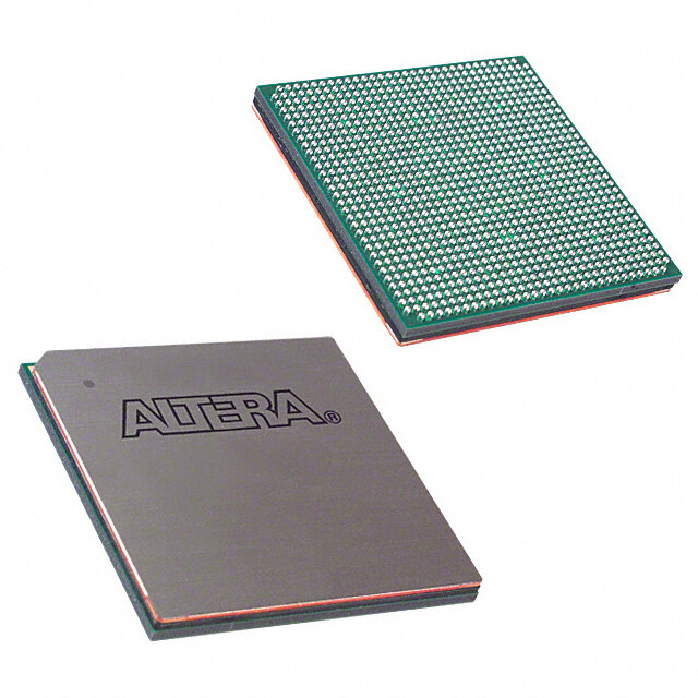
| 数据手册 | 点击此处下载产品Datasheet点击此处下载产品Datasheet点击此处下载产品Datasheethttp://www.altera.com/literature/ds/pkgds.pdf#page=105-106点击此处下载产品Datasheet |
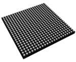
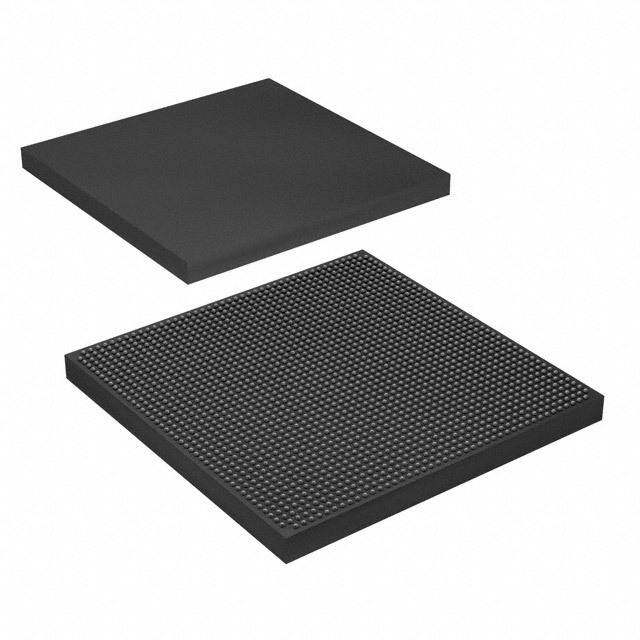
| 产品图片 |
|
| 产品型号 | EP2S15F484I4N |
| rohs | 无铅 / 符合限制有害物质指令(RoHS)规范要求 |
| 产品系列 | Stratix® II |
| 产品培训模块 | http://www.digikey.cn/PTM/IndividualPTM.page?site=cn&lang=zhs&ptm=25450 |
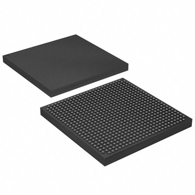
| 供应商器件封装 | 484-FBGA(23x23) |
| 其它名称 | 544-1878 |
| 安装类型 | 表面贴装 |
| 封装/外壳 | 484-BBGA,FCBGA |
| 工作温度 | -40°C ~ 100°C |
| 总RAM位数 | 419328 |
| 栅极数 | - |
| 标准包装 | 20 |
| 电压-电源 | 1.15 V ~ 1.25 V |
| 逻辑元件/单元数 | 15600 |


- 商务部:美国ITC正式对集成电路等产品启动337调查
- 曝三星4nm工艺存在良率问题 高通将骁龙8 Gen1或转产台积电
- 太阳诱电将投资9.5亿元在常州建新厂生产MLCC 预计2023年完工
- 英特尔发布欧洲新工厂建设计划 深化IDM 2.0 战略
- 台积电先进制程称霸业界 有大客户加持明年业绩稳了
- 达到5530亿美元!SIA预计今年全球半导体销售额将创下新高
- 英特尔拟将自动驾驶子公司Mobileye上市 估值或超500亿美元
- 三星加码芯片和SET,合并消费电子和移动部门,撤换高东真等 CEO
- 三星电子宣布重大人事变动 还合并消费电子和移动部门
- 海关总署:前11个月进口集成电路产品价值2.52万亿元 增长14.8%


PDF Datasheet 数据手册内容提取
Stratix II Device Handbook, Volume 1 101 Innovation Drive San Jose, CA 95134 www.altera.com SII5V1-4.5
Copyright © 2011 Altera Corporation. All rights reserved. Altera, The Programmable Solutions Company, the stylized Altera logo, specific device des- ignations, and all other words and logos that are identified as trademarks and/or service marks are, unless noted otherwise, the trademarks and service marks of Altera Corporation in the U.S. and other countries. All other product or service names are the property of their respective holders. Al- tera products are protected under numerous U.S. and foreign patents and pending applications, maskwork rights, and copyrights. Altera warrants performance of its semiconductor products to current specifications in accordance with Altera's standard warranty, but reserves the right to make changes to any products and services at any time without notice. Altera assumes no responsibility or liabil- ity arising out of the application or use of any information, product, or service described herein except as expressly agreed to in writing by Altera Corporation. Altera customers are advised to obtain the latest ver- sion of device specifications before relying on any published information and before placing orders for products or services. ii Altera Corporation
Contents Chapter Revision Dates .......................................................................... vii About this Handbook ................................................................................ i How to Contact Altera ...............................................................................................................................i Typographic Conventions .........................................................................................................................i Section I. Stratix II Device Family Data Sheet Revision History .......................................................................................................................Section I–1 Chapter 1. Introduction Introduction............................................................................................................................................1–1 Features ...................................................................................................................................................1–1 Document Revision History.................................................................................................................1–6 Chapter 2. StratixII Architecture Functional Description..........................................................................................................................2–1 Logic Array Blocks ................................................................................................................................2–3 LAB Interconnects ............................................................................................................................2–4 LAB Control Signals.........................................................................................................................2–5 Adaptive Logic Modules ......................................................................................................................2–6 ALM Operating Modes ...................................................................................................................2–9 Register Chain.................................................................................................................................2–20 Clear & Preset Logic Control ........................................................................................................2–22 MultiTrack Interconnect .....................................................................................................................2–22 TriMatrix Memory...............................................................................................................................2–28 Memory Block Size.........................................................................................................................2–29 Digital Signal Processing Block .........................................................................................................2–40 Modes of Operation .......................................................................................................................2–44 DSP Block Interface ........................................................................................................................2–44 PLLs & Clock Networks .....................................................................................................................2–48 Global & Hierarchical Clocking ...................................................................................................2–48 Enhanced & Fast PLLs ...................................................................................................................2–57 Enhanced PLLs ...............................................................................................................................2–68 Fast PLLs..........................................................................................................................................2–69 I/O Structure ........................................................................................................................................2–69 Double Data Rate I/O Pins ...........................................................................................................2–77 External RAM Interfacing .............................................................................................................2–81 Programmable Drive Strength .....................................................................................................2–83 Altera Corporation iii
Contents Stratix II Device Handbook, Volume1 Open-Drain Output........................................................................................................................2–84 Bus Hold ..........................................................................................................................................2–84 Programmable Pull-Up Resistor ..................................................................................................2–85 Advanced I/O Standard Support ................................................................................................2–85 On-Chip Termination ....................................................................................................................2–89 MultiVolt I/O Interface .................................................................................................................2–93 High-Speed Differential I/O with DPA Support............................................................................2–96 Dedicated Circuitry with DPA Support....................................................................................2–100 Fast PLL & Channel Layout........................................................................................................2–102 Document Revision History.............................................................................................................2–104 Chapter 3. Configuration & Testing IEEE Std. 1149.1 JTAG Boundary-Scan Support ...............................................................................3–1 SignalTap II Embedded Logic Analyzer ............................................................................................3–4 Configuration .........................................................................................................................................3–4 Operating Modes..............................................................................................................................3–5 Configuration Schemes ...................................................................................................................3–7 Configuring StratixII FPGAs with JRunner...............................................................................3–10 Programming Serial Configuration Devices with SRunner.....................................................3–10 Configuring Stratix II FPGAs with the MicroBlaster Driver ...................................................3–11 PLL Reconfiguration ......................................................................................................................3–11 Temperature Sensing Diode (TSD) ...................................................................................................3–11 Automated Single Event Upset (SEU) Detection ............................................................................3–13 Custom-Built Circuitry ..................................................................................................................3–14 Software Interface...........................................................................................................................3–14 Document Revision History...............................................................................................................3–14 Chapter 4. Hot Socketing & Power-OnReset Stratix II Hot-Socketing Specifications ...............................................................................................................4–1 Devices Can Be Driven Before Power-Up ....................................................................................4–2 I/O Pins Remain Tri-Stated During Power-Up ...........................................................................4–2 Signal Pins Do Not Drive the V , V or V Power Supplies....................................4–2 CCIO CCINT CCPD Hot Socketing Feature Implementation in Stratix II Devices..........................................................4–3 Power-On Reset Circuitry ....................................................................................................................4–5 Document Revision History.................................................................................................................4–6 Chapter 5. DC & Switching Characteristics Operating Conditions ...........................................................................................................................5–1 Absolute Maximum Ratings ...........................................................................................................5–1 Recommended Operating Conditions ..........................................................................................5–2 DC Electrical Characteristics ..........................................................................................................5–3 I/O Standard Specifications ...........................................................................................................5–4 Bus Hold Specifications.................................................................................................................5–17 On-Chip Termination Specifications ...........................................................................................5–17 Pin Capacitance ..............................................................................................................................5–19 Power Consumption ...........................................................................................................................5–20 iv Altera Corporation
Contents Contents Timing Model.......................................................................................................................................5–20 Preliminary & Final Timing ..........................................................................................................5–20 I/O Timing Measurement Methodology....................................................................................5–21 Performance ....................................................................................................................................5–27 Internal Timing Parameters ..........................................................................................................5–34 StratixII Clock Timing Parameters..............................................................................................5–41 Clock Network Skew Adders .......................................................................................................5–50 IOE Programmable Delay .............................................................................................................5–51 Default Capacitive Loading of Different I/O Standards..........................................................5–52 I/O Delays.......................................................................................................................................5–54 Maximum Input & Output Clock Toggle Rate ..........................................................................5–66 Duty Cycle Distortion .........................................................................................................................5–77 DCD Measurement Techniques ...................................................................................................5–78 High-Speed I/O Specifications..........................................................................................................5–87 PLL Timing Specifications..................................................................................................................5–91 External Memory Interface Specifications .......................................................................................5–94 JTAG Timing Specifications ...............................................................................................................5–96 Document Revision History...............................................................................................................5–97 Chapter 6. Reference & Ordering Information Software ..................................................................................................................................................6–1 Device Pin-Outs .....................................................................................................................................6–1 Ordering Information ...........................................................................................................................6–1 Document Revision History.................................................................................................................6–2 Altera Corporation v
Contents Stratix II Device Handbook, Volume1 vi Altera Corporation
Chapter Revision Dates The chapters in this book, Stratix II Device Handbook, Volume1, were revised on the following dates. Where chapters or groups of chapters are available separately, part numbers are listed. Chapter 1. Introduction Revised: May 2007 Part number: SII51001-4.2 Chapter 2. StratixII Architecture Revised: May 2007 Part number: SII51002-4.3 Chapter 3. Configuration & Testing Revised: May 2007 Part number: SII51003-4.2 Chapter 4. Hot Socketing & Power-OnReset Revised: May 2007 Part number: SII51004-3.2 Chapter 5. DC & Switching Characteristics Revised: April 2011 Part number: SII51005-4.5 Chapter 6. Reference & Ordering Information Revised: April 2011 Part number: SII51006-2.2 Altera Corporation vii
Chapter Revision Dates Stratix II Device Handbook, Volume1 viii Altera Corporation
About this Handbook This handbook provides comprehensive information about the Altera® Stratix®II family of devices. How to Contact For the most up-to-date information about Altera products, refer to the following table. Altera Contact Contact (1) Address Method Technical support Website www.altera.com/support Technical training Website www.altera.com/training Email custrain@altera.com Product literature Email www.altera.com/literature Altera literature services Website literature@altera.com Non-technical support (General) Email nacomp@altera.com (Software Licensing) Email authorization@altera.com Note to table: (1) You can also contact your local Altera sales office or sales representative. Typographic This document uses the typographic conventions shown below. Conventions Visual Cue Meaning Bold Type with Initial Command names, dialog box titles, checkbox options, and dialog box options are Capital Letters shown in bold, initial capital letters. Example: Save As dialog box. bold type External timing parameters, directory names, project names, disk drive names, filenames, filename extensions, and software utility names are shown in bold type. Examples: f , \qdesigns directory, d: drive, chiptrip.gdf file. MAX Italic Type with Initial Capital Document titles are shown in italic type with initial capital letters. Example: AN 75: Letters High-Speed Board Design. Altera Corporation i Preliminary
Typographic Conventions Stratix II Device Handbook, Volume 1 Visual Cue Meaning Italic type Internal timing parameters and variables are shown in italic type. Examples: t , n + 1. PIA Variable names are enclosed in angle brackets (< >) and shown in italic type. Example: <file name>, <project name>.pof file. Initial Capital Letters Keyboard keys and menu names are shown with initial capital letters. Examples: Delete key, the Options menu. “Subheading Title” References to sections within a document and titles of on-line help topics are shown in quotation marks. Example: “Typographic Conventions.” Courier type Signal and port names are shown in lowercase Courier type. Examples: data1, tdi, input. Active-low signals are denoted by suffix n, e.g., resetn. Anything that must be typed exactly as it appears is shown in Courier type. For example: c:\qdesigns\tutorial\chiptrip.gdf. Also, sections of an actual file, such as a Report File, references to parts of files (e.g., the AHDL keyword SUBDESIGN), as well as logic function names (e.g., TRI) are shown in Courier. 1., 2., 3., and Numbered steps are used in a list of items when the sequence of the items is a., b., c., etc. important, such as the steps listed in a procedure. ■ ● (cid:129) Bullets are used in a list of items when the sequence of the items is not important. v The checkmark indicates a procedure that consists of one step only. 1 The hand points to information that requires special attention. The caution indicates required information that needs special consideration and c understanding and should be read prior to starting or continuing with the procedure or process. w The warning indicates information that should be read prior to starting or continuing the procedure or processes r The angled arrow indicates you should press the Enter key. f The feet direct you to more information on a particular topic. ii Altera Corporation Preliminary
Section I. Stratix II Device Family Data Sheet This section provides the data sheet specifications for Stratix®II devices. This section contains feature definitions of the internal architecture, configuration and JTAG boundary-scan testing information, DC operating conditions, AC timing parameters, a reference to power consumption, and ordering information for StratixII devices. This section contains the following chapters: ■ Chapter1, Introduction ■ Chapter2, StratixII Architecture ■ Chapter3, Configuration & Testing ■ Chapter4, Hot Socketing & Power-OnReset ■ Chapter5, DC & Switching Characteristics ■ Chapter6, Reference & Ordering Information Revision History Refer to each chapter for its own specific revision history. For information on when each chapter was updated, refer to the Chapter Revision Dates section, which appears in the full handbook. Altera Corporation Section I–1
StratixII Device Family Data Sheet Stratix II Device Handbook, Volume 1 Section I–2 Altera Corporation
1. Introduction SII51001-4.2 Introduction The Stratix®II FPGA family is based on a 1.2-V, 90-nm, all-layer copper SRAM process and features a new logic structure that maximizes performance, and enables device densities approaching 180,000 equivalent logic elements (LEs). StratixII devices offer up to 9 Mbits of on-chip, TriMatrix™ memory for demanding, memory intensive applications and has up to 96 DSP blocks with up to 384 (18-bit × 18-bit) multipliers for efficient implementation of high performance filters and other DSP functions. Various high-speed external memory interfaces are supported, including double data rate (DDR) SDRAM and DDR2 SDRAM, RLDRAM II, quad data rate (QDR) II SRAM, and single data rate (SDR) SDRAM. StratixII devices support various I/O standards along with support for 1-gigabit per second (Gbps) source synchronous signaling with DPA circuitry. StratixII devices offer a complete clock management solution with internal clock frequency of up to 550MHz and up to 12phase-locked loops (PLLs). StratixII devices are also the industry’s first FPGAs with the ability to decrypt a configuration bitstream using the Advanced Encryption Standard (AES) algorithm to protect designs. Features The StratixII family offers the following features: ■ 15,600 to 179,400 equivalent LEs; see Table1–1 ■ New and innovative adaptive logic module (ALM), the basic building block of the StratixII architecture, maximizes performance and resource usage efficiency ■ Up to 9,383,040 RAM bits (1,172,880 bytes) available without reducing logic resources ■ TriMatrix memory consisting of three RAM block sizes to implement true dual-port memory and first-in first-out (FIFO) buffers ■ High-speed DSP blocks provide dedicated implementation of multipliers (at up to 450MHz), multiply-accumulate functions, and finite impulse response (FIR) filters ■ Up to 16 global clocks with 24 clocking resources per device region ■ Clock control blocks support dynamic clock network enable/disable, which allows clock networks to power down to reduce power consumption in user mode ■ Up to 12 PLLs (four enhanced PLLs and eight fast PLLs) per device provide spread spectrum, programmable bandwidth, clock switch- over, real-time PLL reconfiguration, and advanced multiplication and phase shifting Altera Corporation 1–1 May 2007
Features ■ Support for numerous single-ended and differential I/O standards ■ High-speed differential I/O support with DPA circuitry for 1-Gbps performance ■ Support for high-speed networking and communications bus standards including Parallel RapidIO, SPI-4 Phase 2 (POS-PHY Level4), HyperTransport™ technology, and SFI-4 ■ Support for high-speed external memory, including DDR and DDR2 SDRAM, RLDRAM II, QDR II SRAM, and SDR SDRAM ■ Support for multiple intellectual property megafunctions from Altera MegaCore® functions and Altera Megafunction Partners Program (AMPPSM) megafunctions ■ Support for design security using configuration bitstream encryption ■ Support for remote configuration updates Table1–1. StratixII FPGA Family Features Feature EP2S15 EP2S30 EP2S60 EP2S90 EP2S130 EP2S180 ALMs 6,240 13,552 24,176 36,384 53,016 71,760 Adaptive look-up tables (ALUTs) (1) 12,480 27,104 48,352 72,768 106,032 143,520 Equivalent LEs (2) 15,600 33,880 60,440 90,960 132,540 179,400 M512 RAM blocks 104 202 329 488 699 930 M4K RAM blocks 78 144 255 408 609 768 M-RAM blocks 0 1 2 4 6 9 Total RAM bits 419,328 1,369,728 2,544,192 4,520,488 6,747,840 9,383,040 DSP blocks 12 16 36 48 63 96 18-bit × 18-bit multipliers (3) 48 64 144 192 252 384 Enhanced PLLs 2 2 4 4 4 4 Fast PLLs 4 4 8 8 8 8 Maximum user I/O pins 366 500 718 902 1,126 1,170 Notes to Table1–1: (1) One ALM contains two ALUTs. The ALUT is the cell used in the Quartus®II software for logic synthesis. (2) This is the equivalent number of LEs in a Stratix device (four-input LUT-based architecture). (3) These multipliers are implemented using the DSP blocks. 1–2 Altera Corporation Stratix II Device Handbook, Volume 1 May 2007
Introduction StratixII devices are available in space-saving FineLine BGA® packages (see Tables1–2 and 1–3). Table1–2. StratixII Package Options & I/O Pin Counts Notes(1), (2) 484-Pin 672-Pin 780-Pin 484-Pin Hybrid 1,020-Pin 1,508-Pin Device FineLine FineLine FineLine BGA FineLine FineLine BGA FineLine BGA BGA BGA BGA EP2S15 342 366 EP2S30 342 500 EP2S60 (3) 334 492 718 EP2S90 (3) 308 534 758 902 EP2S130 (3) 534 742 1,126 EP2S180 (3) 742 1,170 Notes to Table1–2: (1) All I/O pin counts include eight dedicated clock input pins (clk1p, clk1n, clk3p, clk3n, clk9p, clk9n, clk11p, and clk11n) that can be used for data inputs. (2) The QuartusII software I/O pin counts include one additional pin, PLL_ENA, which is not available as general- purpose I/O pins. The PLL_ENA pin can only be used to enable the PLLs within the device. (3) The I/O pin counts for the EP2S60, EP2S90, EP2S130, and EP2S180 devices in the 1020-pin and 1508-pin packages include eight dedicated fast PLL clock inputs (FPLL7CLKp/n, FPLL8CLKp/n, FPLL9CLKp/n, and FPLL10CLKp/n) that can be used for data inputs. Table1–3. StratixII FineLine BGA Package Sizes 484-Pin Dimension 484 Pin 672 Pin 780 Pin 1,020 Pin 1,508 Pin Hybrid Pitch (mm) 1.00 1.00 1.00 1.00 1.00 1.00 Area (mm2) 529 729 729 841 1,089 1,600 Length × width 23 × 23 27 × 27 27 × 27 29 × 29 33 × 33 40 × 40 (mm × mm) All StratixII devices support vertical migration within the same package (for example, you can migrate between the EP2S15, EP2S30, and EP2S60 devices in the 672-pin FineLine BGA package). Vertical migration means that you can migrate to devices whose dedicated pins, configuration pins, and power pins are the same for a given package across device densities. To ensure that a board layout supports migratable densities within one package offering, enable the applicable vertical migration path within the QuartusII software (Assignments menu > Device > Migration Devices). Altera Corporation 1–3 May 2007 Stratix II Device Handbook, Volume 1
Features After compilation, check the information messages for a full list of I/O, DQ, LVDS, and other pins that are not available because of the selected migration path. Table1–4 lists the Stratix II device package offerings and shows the total number of non-migratable user I/O pins when migrating from one density device to a larger density device. Additional I/O pins may not be migratable if migrating from the larger device to the smaller density device. 1 When moving from one density to a larger density, the larger density device may have fewer user I/O pins. The larger device requires more power and ground pins to support the additional logic within the device. Use the QuartusII Pin Planner to determine which user I/O pins are migratable between the two devices. Table1–4.Total Number of Non-Migratable I/O Pins for Stratix II Vertical Migration Paths Vertical Migration 484-Pin 672-Pin 780-Pin 1020-Pin 1508-Pin Path FineLine BGA FineLine BGA FineLine BGA FineLine BGA FineLine BGA EP2S15 to EP2S30 0 (1) 0 EP2S15 to EP2S60 8 (1) 0 EP2S30 to EP2S60 8 (1) 8 EP2S60 to EP2S90 0 EP2S60 to EP2S130 0 EP2S60 to EP2S180 0 EP2S90 to EP2S130 0 (1) 16 17 EP2S90 to EP2S180 16 0 EP2S130 to EP2S180 0 0 Note to Table1–4: (1) Some of the DQ/DQS pins are not migratable. Refer to the Quartus II software information messages for more detailed information. 1 To determine if your user I/O assignments are correct, run the I/O Assignment Analysis command in the QuartusII software (Processing > Start > Start I/O Assignment Analysis). f Refer to the I/O Management chapter in volume 2 of the QuartusII Handbook for more information on pin migration. 1–4 Altera Corporation Stratix II Device Handbook, Volume 1 May 2007
Introduction StratixII devices are available in up to three speed grades, -3, -4, and -5, with -3 being the fastest. Table1–5 shows StratixII device speed-grade offerings. Table1–5. StratixII Device Speed Grades 484-Pin 484-Pin 672-Pin 780-Pin 1,020-Pin 1,508-Pin Temperature Hybrid Device FineLine FineLine FineLine FineLine FineLine Grade FineLine BGA BGA BGA BGA BGA BGA EP2S15 Commercial -3, -4, -5 -3, -4, -5 Industrial -4 -4 EP2S30 Commercial -3, -4, -5 -3, -4, -5 Industrial -4 -4 EP2S60 Commercial -3, -4, -5 -3, -4, -5 -3, -4, -5 Industrial -4 -4 -4 EP2S90 Commercial -4, -5 -4, -5 -3, -4, -5 -3, -4, -5 Industrial -4 -4 EP2S130 Commercial -4, -5 -3, -4, -5 -3, -4, -5 Industrial -4 -4 EP2S180 Commercial -3, -4, -5 -3, -4, -5 Industrial -4 -4 Altera Corporation 1–5 May 2007 Stratix II Device Handbook, Volume 1
Document Revision History Document Table1–6 shows the revision history for this chapter. Revision History Table1–6.Document Revision History Date and Document Changes Made Summary of Changes Version May 2007, v4.2 Moved Document Revision History to the end of the — chapter. April 2006, v4.1 ● Updated “Features” section. — ● Removed Note 4 from Table1–2. ● Updated Table1–4. December 2005, ● Updated Tables1–2, 1–4, and 1–5. — v4.0 ● Updated Figure2–43. July 2005, v3.1 ● Added vertical migration information, including — Table1–4. ● Updated Table1–5. May 2005, v3.0 ● Updated “Features” section. — ● Updated Table1–2. March 2005, Updated “Introduction” and “Features” sections. — v2.1 January 2005, Added note to Table1–2. — v2.0 October 2004, Updated Tables1–2, 1–3, and 1–5. — v1.2 July 2004, v1.1 ● Updated Tables1–1 and 1–2. — ● Updated “Features” section. February 2004, Added document to the StratixII Device Handbook. — v1.0 1–6 Altera Corporation Stratix II Device Handbook, Volume 1 May 2007
2. Stratix II Architecture SII51002-4.3 Functional Stratix®II devices contain a two-dimensional row- and column-based architecture to implement custom logic. A series of column and row Description interconnects of varying length and speed provides signal interconnects between logic array blocks (LABs), memory block structures (M512 RAM, M4K RAM, and M-RAM blocks), and digital signal processing (DSP) blocks. Each LAB consists of eight adaptive logic modules (ALMs). An ALM is the StratixII device family’s basic building block of logic providing efficient implementation of user logic functions. LABs are grouped into rows and columns across the device. M512 RAM blocks are simple dual-port memory blocks with 512 bits plus parity (576 bits). These blocks provide dedicated simple dual-port or single-port memory up to 18-bits wide at up to 500 MHz. M512 blocks are grouped into columns across the device in between certain LABs. M4K RAM blocks are true dual-port memory blocks with 4K bits plus parity (4,608 bits). These blocks provide dedicated true dual-port, simple dual-port, or single-port memory up to 36-bits wide at up to 550 MHz. These blocks are grouped into columns across the device in between certain LABs. M-RAM blocks are true dual-port memory blocks with 512K bits plus parity (589,824 bits). These blocks provide dedicated true dual-port, simple dual-port, or single-port memory up to 144-bits wide at up to 420MHz. Several M-RAM blocks are located individually in the device's logic array. DSP blocks can implement up to either eight full-precision 9 × 9-bit multipliers, four full-precision 18 × 18-bit multipliers, or one full-precision 36 × 36-bit multiplier with add or subtract features. The DSP blocks support Q1.15 format rounding and saturation in the multiplier and accumulator stages. These blocks also contain shift registers for digital signal processing applications, including finite impulse response (FIR) and infinite impulse response (IIR) filters. DSP blocks are grouped into columns across the device and operate at up to 450MHz. Altera Corporation 2–1 May 2007
Functional Description Each StratixII device I/O pin is fed by an I/O element (IOE) located at the end of LAB rows and columns around the periphery of the device. I/O pins support numerous single-ended and differential I/O standards. Each IOE contains a bidirectional I/O buffer and six registers for registering input, output, and output-enable signals. When used with dedicated clocks, these registers provide exceptional performance and interface support with external memory devices such as DDR and DDR2 SDRAM, RLDRAM II, and QDR II SRAM devices. High-speed serial interface channels with dynamic phase alignment (DPA) support data transfer at up to 1 Gbps using LVDS or HyperTransportTM technology I/O standards. Figure2–1 shows an overview of the StratixII device. Figure2–1.StratixII Block Diagram M4K RAM Blocks IOEs Support DDR, PCI, PCI-X, M512 RAM Blocks for DSP Blocks for for True Dual-Port SSTL-3, SSTL-2, HSTL-1, HSTL-2, Dual-Port Memory, Shift Multiplication and Full Memory & Other Embedded LVDS, HyperTransport & other Registers, & FIFO Buffers Implementation of FIR Filters Memory Functions I/O Standards IOEs IOEs IOEs IOEs IOEs LABs LABs LABs LABs LABs LABs IOEs LABs LABs LABs LABs LABs LABs IOEs LABs LABs LABs LABs LABs LABs IOEs LABs LABs LABs LABs LABs LABs IOEs LABs LABs LABs LABs LABs LABs IOEs LABs LABs LABs LABs IOEs LABs LABs LABs LABs IOEs LABs LABs LABs LABs IOEs LABs LABs LABs LABs IOEs LABs LABs LABs LABs M-RAM Block IOEs LABs LABs LABs LABs IOEs LABs LABs LABs LABs IOEs LABs LABs LABs LABs IOEs LABs LABs LABs LABs IOEs LABs LABs LABs LABs LABs LABs IOEs LABs LABs LABs LABs LABs LABs IOEs LABs LABs LABs LABs LABs LABs DSP Block 2–2 Altera Corporation Stratix II Device Handbook, Volume 1 May 2007
StratixII Architecture The number of M512 RAM, M4K RAM, and DSP blocks varies by device along with row and column numbers and M-RAM blocks. Table2–1 lists the resources available in StratixII devices. Table2–1.StratixII Device Resources M512 RAM M4K RAM M-RAM DSP Block LAB Device LAB Rows Columns/Blocks Columns/Blocks Blocks Columns/Blocks Columns EP2S15 4 / 104 3 / 78 0 2 / 12 30 26 EP2S30 6 / 202 4 / 144 1 2 / 16 49 36 EP2S60 7 / 329 5 / 255 2 3 / 36 62 51 EP2S90 8 / 488 6 / 408 4 3 / 48 71 68 EP2S130 9 / 699 7 / 609 6 3 / 63 81 87 EP2S180 11 / 930 8 / 768 9 4 / 96 100 96 Logic Array Each LAB consists of eight ALMs, carry chains, shared arithmetic chains, LAB control signals, local interconnect, and register chain connection Blocks lines. The local interconnect transfers signals between ALMs in the same LAB. Register chain connections transfer the output of an ALM register to the adjacent ALM register in an LAB. The Quartus®II Compiler places associated logic in an LAB or adjacent LABs, allowing the use of local, shared arithmetic chain, and register chain connections for performance and area efficiency. Figure2–2 shows the StratixII LAB structure. Altera Corporation 2–3 May 2007 Stratix II Device Handbook, Volume 1
Logic Array Blocks Figure2–2.StratixII LAB Structure Row Interconnects of Variable Speed & Length ALMs Direct link interconnect from adjacent block Direct link interconnect from adjacent block Direct link Direct link interconnect to interconnect to adjacent block adjacent block Local Interconnect LAB Local Interconnect is Driven Column Interconnects of from Either Side by Columns & LABs, Variable Speed & Length & from Above by Rows LAB Interconnects The LAB local interconnect can drive ALMs in the same LAB. It is driven by column and row interconnects and ALM outputs in the same LAB. Neighboring LABs, M512 RAM blocks, M4K RAM blocks, M-RAM blocks, or DSP blocks from the left and right can also drive an LAB's local interconnect through the direct link connection. The direct link connection feature minimizes the use of row and column interconnects, providing higher performance and flexibility. Each ALM can drive 24ALMs through fast local and direct link interconnects. Figure2–3 shows the direct link connection. 2–4 Altera Corporation Stratix II Device Handbook, Volume 1 May 2007
StratixII Architecture Figure2–3.Direct Link Connection Direct link interconnect from Direct link interconnect from left LAB, TriMatrix memory right LAB, TriMatrix memory block, DSP block, or IOE output block, DSP block, or IOE output ALMs Direct link Direct link interconnect interconnect to left to right Local Interconnect LAB Control Signals Each LAB contains dedicated logic for driving control signals to its ALMs. The control signals include three clocks, three clock enables, two asynchronous clears, synchronous clear, asynchronous preset/load, and synchronous load control signals. This gives a maximum of 11 control signals at a time. Although synchronous load and clear signals are generally used when implementing counters, they can also be used with other functions. Each LAB can use three clocks and three clock enable signals. However, there can only be up to two unique clocks per LAB, as shown in the LAB control signal generation circuit in Figure2–4. Each LAB's clock and clock enable signals are linked. For example, any ALM in a particular LAB using the labclk1 signal also uses labclkena1. If the LAB uses both the rising and falling edges of a clock, it also uses two LAB-wide clock signals. De-asserting the clock enable signal turns off the corresponding LAB-wide clock. Each LAB can use two asynchronous clear signals and an asynchronous load/preset signal. By default, the QuartusII software uses a NOT gate push-back technique to achieve preset. If you disable the NOT gate push-up option or assign a given register to power up high using the QuartusII software, the preset is achieved using the asynchronous load Altera Corporation 2–5 May 2007 Stratix II Device Handbook, Volume 1
Adaptive Logic Modules signal with asynchronous load data input tied high. When the asynchronous load/preset signal is used, the labclkena0 signal is no longer available. The LAB row clocks [5..0] and LAB local interconnect generate the LAB-wide control signals. The MultiTrackTM interconnect's inherent low skew allows clock and control signal distribution in addition to data. Figure2–4 shows the LAB control signal generation circuit. Figure2–4.LAB-Wide Control Signals There are two unique clock signals per LAB. 6 Dedicated Row LAB Clocks 6 6 Local Interconnect Local Interconnect Local Interconnect Local Interconnect Local Interconnect Local Interconnect labclk0 labclk1 labclk2 syncload labclr1 labclkena0 labclkena1 labclkena2 labclr0 synclr or asyncload or labpreset Adaptive Logic The basic building block of logic in the StratixII architecture, the adaptive logic module (ALM), provides advanced features with efficient logic Modules utilization. Each ALM contains a variety of look-up table (LUT)-based resources that can be divided between two adaptive LUTs (ALUTs). With up to eight inputs to the two ALUTs, one ALM can implement various combinations of two functions. This adaptability allows the ALM to be 2–6 Altera Corporation Stratix II Device Handbook, Volume 1 May 2007
StratixII Architecture completely backward-compatible with four-input LUT architectures. One ALM can also implement any function of up to six inputs and certain seven-input functions. In addition to the adaptive LUT-based resources, each ALM contains two programmable registers, two dedicated full adders, a carry chain, a shared arithmetic chain, and a register chain. Through these dedicated resources, the ALM can efficiently implement various arithmetic functions and shift registers. Each ALM drives all types of interconnects: local, row, column, carry chain, shared arithmetic chain, register chain, and direct link interconnects. Figure2–5 shows a high-level block diagram of the StratixII ALM while Figure2–6 shows a detailed view of all the connections in the ALM. Figure2–5.High-Level Block Diagram of the StratixII ALM carry_in shared_arith_in reg_chain_in To general or local routing dataf0 adder0 D Q To general or datae0 local routing dataa reg0 datab Combinational Logic datac datad adder1 D Q To general or local routing datae1 reg1 dataf1 To general or local routing carry_out shared_arith_out reg_chain_out Altera Corporation 2–7 May 2007 Stratix II Device Handbook, Volume 1
Adaptive Logic Modules Figure2–6.StratixII ALM Details Row, column &direct link routing Row, column &direct link routing LocalInterconnect Row, column &direct link routing Row, column &direct link routing LocalInterconnect asyncload ena[2..0] PRN/ALDDQADATA ENACLRN PRN/ALDDQADATA ENACLRN clk[2..0] aclr[1..0] reg_chain_insclr syncload reg_chain_out VCC carry_in carry_out shared_arith_in shared_arith_out 4-InputLUT 3-InputLUT 3-InputLUT 4-InputLUT 3-InputLUT 3-InputLUT dataf0 datae0 datac dataa datab datad datae1 dataf1 LocalInterconnect LocalInterconnect LocalInterconnect LocalInterconnect LocalInterconnect lacoLtcennocretnI LocalInterconnect LocalInterconnect 2–8 Altera Corporation Stratix II Device Handbook, Volume 1 May 2007
StratixII Architecture One ALM contains two programmable registers. Each register has data, clock, clock enable, synchronous and asynchronous clear, asynchronous load data, and synchronous and asynchronous load/preset inputs. Global signals, general-purpose I/O pins, or any internal logic can drive the register's clock and clear control signals. Either general-purpose I/O pins or internal logic can drive the clock enable, preset, asynchronous load, and asynchronous load data. The asynchronous load data input comes from the datae or dataf input of the ALM, which are the same inputs that can be used for register packing. For combinational functions, the register is bypassed and the output of the LUT drives directly to the outputs of the ALM. Each ALM has two sets of outputs that drive the local, row, and column routing resources. The LUT, adder, or register output can drive these output drivers independently (see Figure2–6). For each set of output drivers, two ALM outputs can drive column, row, or direct link routing connections, and one of these ALM outputs can also drive local interconnect resources. This allows the LUT or adder to drive one output while the register drives another output. This feature, called register packing, improves device utilization because the device can use the register and the combinational logic for unrelated functions. Another special packing mode allows the register output to feed back into the LUT of the same ALM so that the register is packed with its own fan-out LUT. This provides another mechanism for improved fitting. The ALM can also drive out registered and unregistered versions of the LUT or adder output. f See the Performance & Logic Efficiency Analysis of StratixII Devices White Paper for more information on the efficiencies of the StratixII ALM and comparisons with previous architectures. ALM Operating Modes The StratixII ALM can operate in one of the following modes: ■ Normal mode ■ Extended LUT mode ■ Arithmetic mode ■ Shared arithmetic mode Each mode uses ALM resources differently. In each mode, eleven available inputs to the ALM--the eight data inputs from the LAB local interconnect; carry-in from the previous ALM or LAB; the shared arithmetic chain connection from the previous ALM or LAB; and the register chain connection--are directed to different destinations to implement the desired logic function. LAB-wide signals provide clock, asynchronous clear, asynchronous preset/load, synchronous clear, Altera Corporation 2–9 May 2007 Stratix II Device Handbook, Volume 1
Adaptive Logic Modules synchronous load, and clock enable control for the register. These LAB- wide signals are available in all ALM modes. See the “LAB Control Signals” section for more information on the LAB-wide control signals. The QuartusII software and supported third-party synthesis tools, in conjunction with parameterized functions such as library of parameterized modules (LPM) functions, automatically choose the appropriate mode for common functions such as counters, adders, subtractors, and arithmetic functions. If required, you can also create special-purpose functions that specify which ALM operating mode to use for optimal performance. Normal Mode The normal mode is suitable for general logic applications and combinational functions. In this mode, up to eight data inputs from the LAB local interconnect are inputs to the combinational logic. The normal mode allows two functions to be implemented in one StratixII ALM, or an ALM to implement a single function of up to six inputs. The ALM can support certain combinations of completely independent functions and various combinations of functions which have common inputs. Figure2–7 shows the supported LUT combinations in normal mode. 2–10 Altera Corporation Stratix II Device Handbook, Volume 1 May 2007
StratixII Architecture Figure2–7.ALM in Normal Mode Note(1) dataf0 dataf0 datae0 4-Input combout0 dadtaatea0c 5-Input combout0 datac LUT LUT dataa dataa datab datab datad 4-Input combout1 datae1 LUT datad 5-Input combout1 dataf1 datae1 LUT dataf1 dataf0 datae0 5-Input dataf0 datac combout0 LUT datae0 dataa dataa 6-Input datab combout0 datab LUT datac datad datad 3-Input datae1 combout1 LUT dataf1 dataf0 datae0 dataa 6-Input combout0 dataf0 datab LUT datae0 datac datac 5-Input combout0 datad LUT dataa datab 6-Input combout1 datad 4-Input LUT datae1 LUT combout1 datae1 dataf1 dataf1 Note to Figure2–7: (1) Combinations of functions with fewer inputs than those shown are also supported. For example, combinations of functions with the following number of inputs are supported: 4 and 3, 3 and 3, 3 and 2, 5 and 2, etc. The normal mode provides complete backward compatibility with four- input LUT architectures. Two independent functions of four inputs or less can be implemented in one StratixII ALM. In addition, a five-input function and an independent three-input function can be implemented without sharing inputs. Altera Corporation 2–11 May 2007 Stratix II Device Handbook, Volume 1
Adaptive Logic Modules For the packing of two five-input functions into one ALM, the functions must have at least two common inputs. The common inputs are dataa and datab. The combination of a four-input function with a five-input function requires one common input (either dataa or datab). In the case of implementing two six-input functions in one ALM, four inputs must be shared and the combinational function must be the same. For example, a 4×2crossbar switch (two 4-to-1 multiplexers with common inputs and unique select lines) can be implemented in one ALM, as shown in Figure2–8. The shared inputs are dataa, datab, datac, and datad, while the unique select lines are datae0 and dataf0 for function0, and datae1 and dataf1 for function1. This crossbar switch consumes four LUTs in a four-input LUT-based architecture. Figure2–8.4 × 2 Crossbar Switch Example 4 × 2 Crossbar Switch Implementation in 1 ALM sel0[1..0] dataf0 inputa datae0 inputb out0 dataa Six-Input LUT combout0 datab inputc datac (Function0) inputd datad out1 sel1[1..0] Six-Input LUT combout1 datae1 (Function1) dataf1 In a sparsely used device, functions that could be placed into one ALM may be implemented in separate ALMs. The QuartusII Compiler spreads a design out to achieve the best possible performance. As a device begins to fill up, the QuartusII software automatically utilizes the full potential of the StratixII ALM. The QuartusII Compiler automatically searches for functions of common inputs or completely independent functions to be placed into one ALM and to make efficient use of the device resources. In addition, you can manually control resource usage by setting location assignments. Any six-input function can be implemented utilizing inputs dataa, datab, datac, datad, and either datae0 and dataf0 or datae1 and dataf1. If datae0 and dataf0 are utilized, the output is driven to register0, and/or register0 is bypassed and the data drives out to the interconnect using the top set of output drivers (see Figure2–9). If 2–12 Altera Corporation Stratix II Device Handbook, Volume 1 May 2007
StratixII Architecture datae1 and dataf1 are utilized, the output drives to register1 and/or bypasses register1 and drives to the interconnect using the bottom set of output drivers. The QuartusII Compiler automatically selects the inputs to the LUT. Asynchronous load data for the register comes from the datae or dataf input of the ALM. ALMs in normal mode support register packing. Figure2–9.6-Input Function in Normal Mode Notes(1), (2) dataf0 To general or datae0 local routing dataa 6-Input datab LUT To general or D Q datac local routing datad reg0 datae1 dataf1 To general or (2) D Q local routing These inputs are available for register packing. reg1 Notes to Figure2–9: (1) If datae1 and dataf1 are used as inputs to the six-input function, then datae0 and dataf0 are available for register packing. (2) The dataf1 input is available for register packing only if the six-input function is un-registered. Extended LUT Mode The extended LUT mode is used to implement a specific set of seven-input functions. The set must be a 2-to-1 multiplexer fed by two arbitrary five-input functions sharing four inputs. Figure2–10 shows the template of supported seven-input functions utilizing extended LUT mode. In this mode, if the seven-input function is unregistered, the unused eighth input is available for register packing. Functions that fit into the template shown in Figure2–10 occur naturally in designs. These functions often appear in designs as “if-else” statements in Verilog HDL or VHDL code. Altera Corporation 2–13 May 2007 Stratix II Device Handbook, Volume 1
Adaptive Logic Modules Figure2–10.Template for Supported Seven-Input Functions in Extended LUT Mode datae0 datac dataa 5-Input datab To general or datad LUT local routing dataf0 combout0 To general or D Q local routing 5-Input LUT reg0 datae1 dataf1 (1) This input is available for register packing. Note to Figure2–10: (1) If the seven-input function is unregistered, the unused eighth input is available for register packing. The second register, reg1, is not available. Arithmetic Mode The arithmetic mode is ideal for implementing adders, counters, accumulators, wide parity functions, and comparators. An ALM in arithmetic mode uses two sets of two four-input LUTs along with two dedicated full adders. The dedicated adders allow the LUTs to be available to perform pre-adder logic; therefore, each adder can add the output of two four-input functions. The four LUTs share the dataa and datab inputs. As shown in Figure2–11, the carry-in signal feeds to adder0, and the carry-out from adder0 feeds to carry-in of adder1. The carry-out from adder1 drives to adder0 of the next ALM in the LAB. ALMs in arithmetic mode can drive out registered and/or unregistered versions of the adder outputs. 2–14 Altera Corporation Stratix II Device Handbook, Volume 1 May 2007
StratixII Architecture Figure2–11.ALM in Arithmetic Mode carry_in datae0 adder0 4-Input To general or LUT local routing To general or D Q local routing dataf0 datac 4-Input reg0 datab LUT dataa adder1 4-Input To general or datad LUT local routing datae1 To general or D Q local routing 4-Input reg1 LUT dataf1 carry_out While operating in arithmetic mode, the ALM can support simultaneous use of the adder's carry output along with combinational logic outputs. In this operation, the adder output is ignored. This usage of the adder with the combinational logic output provides resource savings of up to 50% for functions that can use this ability. An example of such functionality is a conditional operation, such as the one shown in Figure2–12. The equation for this example is: R = (X < Y) ? Y : X To implement this function, the adder is used to subtract ‘Y’ from ‘X.’ If ‘X’ is less than ‘Y,’ the carry_out signal is ‘1.’ The carry_out signal is fed to an adder where it drives out to the LAB local interconnect. It then feeds to the LAB-wide syncload signal. When asserted, syncload selects the syncdata input. In this case, the data ‘Y’ drives the syncdata inputs to the registers. If ‘X’ is greater than or equal to ‘Y,’ the syncload signal is de-asserted and ‘X’ drives the data port of the registers. Altera Corporation 2–15 May 2007 Stratix II Device Handbook, Volume 1
Adaptive Logic Modules Figure2–12.Conditional Operation Example Adder output is not used. ALM 1 X[0] Comb & X[0] Adder R[0] To general or Y[0] Logic D Q local routing reg0 syncdata syncload X[1] Comb & X[1] Adder R[1] To general or Y[1] Logic D Q local routing reg1 Carry Chain syncload ALM 2 X[2] Comb & X[2] Adder R[2] To general or Y[2] Logic D Q local routing reg0 syncload Comb & To local routing & carry_out Adder then to LAB-wide syncload Logic The arithmetic mode also offers clock enable, counter enable, synchronous up/down control, add/subtract control, synchronous clear, synchronous load. The LAB local interconnect data inputs generate the clock enable, counter enable, synchronous up/down and add/subtract control signals. These control signals are good candidates for the inputs that are shared between the four LUTs in the ALM. The synchronous clear and synchronous load options are LAB-wide signals that affect all registers in the LAB. The QuartusII software automatically places any registers that are not used by the counter into other LABs. Carry Chain The carry chain provides a fast carry function between the dedicated adders in arithmetic or shared arithmetic mode. Carry chains can begin in either the first ALM or the fifth ALM in an LAB. The final carry-out signal is routed to an ALM, where it is fed to local, row, or column interconnects. 2–16 Altera Corporation Stratix II Device Handbook, Volume 1 May 2007
StratixII Architecture The QuartusII Compiler automatically creates carry chain logic during design processing, or you can create it manually during design entry. Parameterized functions such as LPM functions automatically take advantage of carry chains for the appropriate functions. The QuartusII Compiler creates carry chains longer than 16 (8 ALMs in arithmetic or shared arithmetic mode) by linking LABs together automatically. For enhanced fitting, a long carry chain runs vertically allowing fast horizontal connections to TriMatrix memory and DSP blocks. A carry chain can continue as far as a full column. To avoid routing congestion in one small area of the device when a high fan-in arithmetic function is implemented, the LAB can support carry chains that only utilize either the top half or the bottom half of the LAB before connecting to the next LAB. This leaves the other half of the ALMs in the LAB available for implementing narrower fan-in functions in normal mode. Carry chains that use the top four ALMs in the first LAB carry into the top half of the ALMs in the next LAB within the column. Carry chains that use the bottom four ALMs in the first LAB carry into the bottom half of the ALMs in the next LAB within the column. Every other column of LABs is top-half bypassable, while the other LAB columns are bottom-half bypassable. See the “MultiTrack Interconnect” on page2–22 section for more information on carry chain interconnect. Shared Arithmetic Mode In shared arithmetic mode, the ALM can implement a three-input add. In this mode, the ALM is configured with four 4-input LUTs. Each LUT either computes the sum of three inputs or the carry of three inputs. The output of the carry computation is fed to the next adder (either to adder1 in the same ALM or to adder0 of the next ALM in the LAB) via a dedicated connection called the shared arithmetic chain. This shared arithmetic chain can significantly improve the performance of an adder tree by reducing the number of summation stages required to implement an adder tree. Figure2–13 shows the ALM in shared arithmetic mode. Altera Corporation 2–17 May 2007 Stratix II Device Handbook, Volume 1
Adaptive Logic Modules Figure2–13.ALM in Shared Arithmetic Mode shared_arith_in carry_in 4-Input To general or LUT local routing To general or D Q local routing datae0 datac 4-Input reg0 datab LUT dataa 4-Input To general or datad LUT local routing datae1 To general or D Q local routing 4-Input reg1 LUT carry_out shared_arith_out Note to Figure2–13: (1) Inputs dataf0 and dataf1 are available for register packing in shared arithmetic mode. Adder trees can be found in many different applications. For example, the summation of the partial products in a logic-based multiplier can be implemented in a tree structure. Another example is a correlator function that can use a large adder tree to sum filtered data samples in a given time frame to recover or to de-spread data which was transmitted utilizing spread spectrum technology. An example of a three-bit add operation utilizing the shared arithmetic mode is shown in Figure2–14. The partial sum (S[2..0]) and the partial carry (C[2..0]) is obtained using the LUTs, while the result (R[2..0]) is computed using the dedicated adders. 2–18 Altera Corporation Stratix II Device Handbook, Volume 1 May 2007
StratixII Architecture Figure2–14.Example of a 3-bit Add Utilizing Shared Arithmetic Mode shared_arith_in = '0' carry_in = '0' 3-Bit Add Example ALM Implementation ALM 1 X2 X1 X0 3-Input S0 1st stage add is implemented in LUTs. Y2 Y1 Y0 LUT + Z2 Z1 Z0 R0 2nd stage add is S2 S1 S0 X0 implemented in adders. + C2 C1 C0 3-Input C0 Y0 LUT R3 R2 R1 R0 Z0 X1 Decimal 3-Input S1 Y1 Binary Add Equivalents LUT Z1 1 1 0 6 R1 1 0 1 5 3-Input C1 + 0 1 0 + 2 LUT 0 0 1 1 + 1 1 0 + 2 x 6 ALM 2 1 1 0 1 13 3-Input S2 LUT R2 X2 3-Input C2 Y2 LUT Z2 3-Input '0' LUT R3 3-Input LUT Shared Arithmetic Chain In addition to the dedicated carry chain routing, the shared arithmetic chain available in shared arithmetic mode allows the ALM to implement a three-input add. This significantly reduces the resources necessary to implement large adder trees or correlator functions. The shared arithmetic chains can begin in either the first or fifth ALM in an LAB. The QuartusII Compiler creates shared arithmetic chains longer than 16 (8ALMs in arithmetic or shared arithmetic mode) by linking LABs together automatically. For enhanced fitting, a long shared Altera Corporation 2–19 May 2007 Stratix II Device Handbook, Volume 1
Adaptive Logic Modules arithmetic chain runs vertically allowing fast horizontal connections to TriMatrix memory and DSP blocks. A shared arithmetic chain can continue as far as a full column. Similar to the carry chains, the shared arithmetic chains are also top- or bottom-half bypassable. This capability allows the shared arithmetic chain to cascade through half of the ALMs in a LAB while leaving the other half available for narrower fan-in functionality. Every other LAB column is top-half bypassable, while the other LAB columns are bottom- half bypassable. See the “MultiTrack Interconnect” on page2–22 section for more information on shared arithmetic chain interconnect. Register Chain In addition to the general routing outputs, the ALMs in an LAB have register chain outputs. The register chain routing allows registers in the same LAB to be cascaded together. The register chain interconnect allows an LAB to use LUTs for a single combinational function and the registers to be used for an unrelated shift register implementation. These resources speed up connections between ALMs while saving local interconnect resources (see Figure2–15). The QuartusII Compiler automatically takes advantage of these resources to improve utilization and performance. 2–20 Altera Corporation Stratix II Device Handbook, Volume 1 May 2007
StratixII Architecture Figure2–15.Register Chain within an LAB Note(1) From Previous ALM Within The LAB reg_chain_in To general or local routing adder0 D Q To general or local routing reg0 Combinational Logic adder1 D Q To general or local routing reg1 To general or local routing To general or local routing adder0 D Q To general or local routing reg0 Combinational Logic adder1 D Q To general or local routing reg1 To general or local routing reg_chain_out To Next ALM within the LAB Note to Figure2–15: (1) The combinational or adder logic can be utilized to implement an unrelated, un-registered function. See the “MultiTrack Interconnect” on page2–22 section for more information on register chain interconnect. Altera Corporation 2–21 May 2007 Stratix II Device Handbook, Volume 1
MultiTrack Interconnect Clear & Preset Logic Control LAB-wide signals control the logic for the register's clear and load/preset signals. The ALM directly supports an asynchronous clear and preset function. The register preset is achieved through the asynchronous load of a logic high. The direct asynchronous preset does not require a NOT- gate push-back technique. StratixII devices support simultaneous asynchronous load/preset, and clear signals. An asynchronous clear signal takes precedence if both signals are asserted simultaneously. Each LAB supports up to two clears and one load/preset signal. In addition to the clear and load/preset ports, StratixII devices provide a device-wide reset pin (DEV_CLRn) that resets all registers in the device. An option set before compilation in the QuartusII software controls this pin. This device-wide reset overrides all other control signals. MultiTrack In the StratixII architecture, connections between ALMs, TriMatrix memory, DSP blocks, and device I/O pins are provided by the MultiTrack Interconnect interconnect structure with DirectDriveTM technology. The MultiTrack interconnect consists of continuous, performance-optimized routing lines of different lengths and speeds used for inter- and intra-design block connectivity. The QuartusII Compiler automatically places critical design paths on faster interconnects to improve design performance. DirectDrive technology is a deterministic routing technology that ensures identical routing resource usage for any function regardless of placement in the device. The MultiTrack interconnect and DirectDrive technology simplify the integration stage of block-based designing by eliminating the re-optimization cycles that typically follow design changes and additions. The MultiTrack interconnect consists of row and column interconnects that span fixed distances. A routing structure with fixed length resources for all devices allows predictable and repeatable performance when migrating through different device densities. Dedicated row interconnects route signals to and from LABs, DSP blocks, and TriMatrix memory in the same row. These row resources include: ■ Direct link interconnects between LABs and adjacent blocks ■ R4 interconnects traversing four blocks to the right or left ■ R24 row interconnects for high-speed access across the length of the device 2–22 Altera Corporation Stratix II Device Handbook, Volume 1 May 2007
StratixII Architecture The direct link interconnect allows an LAB, DSP block, or TriMatrix memory block to drive into the local interconnect of its left and right neighbors and then back into itself. This provides fast communication between adjacent LABs and/or blocks without using row interconnect resources. The R4 interconnects span four LABs, three LABs and one M512 RAM block, two LABs and one M4K RAM block, or two LABs and one DSP block to the right or left of a source LAB. These resources are used for fast row connections in a four-LAB region. Every LAB has its own set of R4 interconnects to drive either left or right. Figure2–16 shows R4 interconnect connections from an LAB. R4 interconnects can drive and be driven by DSP blocks and RAM blocks and row IOEs. For LAB interfacing, a primary LAB or LAB neighbor can drive a given R4 interconnect. For R4 interconnects that drive to the right, the primary LAB and right neighbor can drive on to the interconnect. For R4 interconnects that drive to the left, the primary LAB and its left neighbor can drive on to the interconnect. R4 interconnects can drive other R4 interconnects to extend the range of LABs they can drive. R4 interconnects can also drive C4 and C16 interconnects for connections from one row to another. Additionally, R4 interconnects can drive R24 interconnects. Figure2–16.R4 Interconnect Connections Notes(1), (2), (3) Adjacent LAB can C4 and C16 R4 Interconnect Drive onto Another Column Interconnects (1) Driving Right LAB's R4 Interconnect R4 Interconnect Driving Left LAB Primary LAB Neighbor LAB (2) Neighbor Notes to Figure2–16: (1) C4 and C16 interconnects can drive R4 interconnects. (2) This pattern is repeated for every LAB in the LAB row. (3) The LABs in Figure2–16 show the 16 possible logical outputs per LAB. Altera Corporation 2–23 May 2007 Stratix II Device Handbook, Volume 1
MultiTrack Interconnect R24 row interconnects span 24 LABs and provide the fastest resource for long row connections between LABs, TriMatrix memory, DSP blocks, and Row IOEs. The R24 row interconnects can cross M-RAM blocks. R24 row interconnects drive to other row or column interconnects at every fourth LAB and do not drive directly to LAB local interconnects. R24 row interconnects drive LAB local interconnects via R4 and C4 interconnects. R24 interconnects can drive R24, R4, C16, and C4 interconnects. The column interconnect operates similarly to the row interconnect and vertically routes signals to and from LABs, TriMatrix memory, DSP blocks, and IOEs. Each column of LABs is served by a dedicated column interconnect. These column resources include: ■ Shared arithmetic chain interconnects in an LAB ■ Carry chain interconnects in an LAB and from LAB to LAB ■ Register chain interconnects in an LAB ■ C4 interconnects traversing a distance of four blocks in up and down direction ■ C16 column interconnects for high-speed vertical routing through the device StratixII devices include an enhanced interconnect structure in LABs for routing shared arithmetic chains and carry chains for efficient arithmetic functions. The register chain connection allows the register output of one ALM to connect directly to the register input of the next ALM in the LAB for fast shift registers. These ALM to ALM connections bypass the local interconnect. The QuartusII Compiler automatically takes advantage of these resources to improve utilization and performance. Figure2–17 shows the shared arithmetic chain, carry chain and register chain interconnects. 2–24 Altera Corporation Stratix II Device Handbook, Volume 1 May 2007
StratixII Architecture Figure2–17.Shared Arithmetic Chain, Carry Chain & Register Chain Interconnects Local Interconnect Routing Among ALMs in the LAB Carry Chain & Shared ALM 1 Register Chain Arithmetic Chain Routing to Adjacent Routing to Adjacent ALM ALM's Register Inpu ALM 2 Local ALM 3 Interconnect ALM 4 ALM 5 ALM 6 ALM 7 ALM 8 The C4 interconnects span four LABs, M512, or M4K blocks up or down from a source LAB. Every LAB has its own set of C4 interconnects to drive either up or down. Figure2–18 shows the C4 interconnect connections from an LAB in a column. The C4 interconnects can drive and be driven by all types of architecture blocks, including DSP blocks, TriMatrix memory blocks, and column and row IOEs. For LAB interconnection, a primary LAB or its LAB neighbor can drive a given C4 interconnect. C4 interconnects can drive each other to extend their range as well as drive row interconnects for column-to-column connections. Altera Corporation 2–25 May 2007 Stratix II Device Handbook, Volume 1
MultiTrack Interconnect Figure2–18.C4 Interconnect Connections Note(1) C4 Interconnect Drives Local and R4 Interconnects up to Four Rows C4 Interconnect Driving Up LAB Row Interconnect Adjacent LAB can drive onto neighboring LAB's C4 interconnect Local Interconnect C4 Interconnect Driving Down Note to Figure2–18: (1) Each C4 interconnect can drive either up or down four rows. 2–26 Altera Corporation Stratix II Device Handbook, Volume 1 May 2007
StratixII Architecture C16 column interconnects span a length of 16 LABs and provide the fastest resource for long column connections between LABs, TriMatrix memory blocks, DSP blocks, and IOEs. C16 interconnects can cross M-RAM blocks and also drive to row and column interconnects at every fourth LAB. C16 interconnects drive LAB local interconnects via C4 and R4 interconnects and do not drive LAB local interconnects directly. All embedded blocks communicate with the logic array similar to LAB- to-LAB interfaces. Each block (that is, TriMatrix memory and DSP blocks) connects to row and column interconnects and has local interconnect regions driven by row and column interconnects. These blocks also have direct link interconnects for fast connections to and from a neighboring LAB. All blocks are fed by the row LAB clocks, labclk[5..0]. Table2–2 shows the StratixII device’s routing scheme. Table2–2. StratixII Device Routing Scheme (Part 1 of2) Destination ain ect Source Shared Arithmetic Ch Carry Chain Register Chain Local Interconnect Direct Link Interconn R4 Interconnect R24 Interconnect C4 Interconnect C16 Interconnect ALM M512 RAM Block M4K RAM Block M-RAM Block DSP Blocks Column IOE Row IOE Shared arithmetic chain v Carry chain v Register chain v Local interconnect v v v v v v v Direct link interconnect v R4 interconnect v v v v v R24 interconnect v v v v C4 interconnect v v v C16 interconnect v v v v ALM v v v v v v v M512 RAM block v v v v M4K RAM block v v v v M-RAM block v v v v DSP blocks v v v Altera Corporation 2–27 May 2007 Stratix II Device Handbook, Volume 1
TriMatrix Memory Table2–2. StratixII Device Routing Scheme (Part 2 of2) Destination ain ect Source Shared Arithmetic Ch Carry Chain Register Chain Local Interconnect Direct Link Interconn R4 Interconnect R24 Interconnect C4 Interconnect C16 Interconnect ALM M512 RAM Block M4K RAM Block M-RAM Block DSP Blocks Column IOE Row IOE Column IOE v v v Row IOE v v v v TriMatrix TriMatrix memory consists of three types of RAM blocks: M512, M4K, and M-RAM. Although these memory blocks are different, they can all Memory implement various types of memory with or without parity, including true dual-port, simple dual-port, and single-port RAM, ROM, and FIFO buffers. Table2–3 shows the size and features of the different RAM blocks. Table2–3.TriMatrix Memory Features (Part 1 of2) M512 RAM Block M4K RAM Block M-RAM Block Memory Feature (32×18 Bits) (128×36 Bits) (4K×144Bits) Maximum performance 500 MHz 550 MHz 420 MHz True dual-port memory v v Simple dual-port memory v v v Single-port memory v v v Shift register v v ROM v v (1) FIFO buffer v v v Pack mode v v Byte enable v v v Address clock enable v v Parity bits v v v Mixed clock mode v v v Memory initialization (.mif) v v 2–28 Altera Corporation Stratix II Device Handbook, Volume 1 May 2007
StratixII Architecture Table2–3.TriMatrix Memory Features (Part 2 of2) M512 RAM Block M4K RAM Block M-RAM Block Memory Feature (32×18 Bits) (128×36 Bits) (4K×144Bits) Simple dual-port memory v v v mixed width support True dual-port memory v v mixed width support Power-up conditions Outputs cleared Outputs cleared Outputs unknown Register clears Output registers Output registers Output registers Mixed-port read-during-write Unknown output/old data Unknown output/old data Unknown output Configurations 512 × 1 4K × 1 64K × 8 256 × 2 2K × 2 64K × 9 128 × 4 1K × 4 32K × 16 64 × 8 512 × 8 32K × 18 64 × 9 512 × 9 16K × 32 32 × 16 256 × 16 16K × 36 32 × 18 256 × 18 8K × 64 128 × 32 8K × 72 128 × 36 4K × 128 4K × 144 Notes to Table2–3: (1) The M-RAM block does not support memory initializations. However, the M-RAM block can emulate a ROM function using a dual-port RAM bock. The StratixII device must write to the dual-port memory once and then disable the write-enable ports afterwards. Memory Block Size TriMatrix memory provides three different memory sizes for efficient application support. The QuartusII software automatically partitions the user-defined memory into the embedded memory blocks using the most efficient size combinations. You can also manually assign the memory to a specific block size or a mixture of block sizes. When applied to input registers, the asynchronous clear signal for the TriMatrix embedded memory immediately clears the input registers. However, the output of the memory block does not show the effects until the next clock edge. When applied to output registers, the asynchronous clear signal clears the output registers and the effects are seen immediately. Altera Corporation 2–29 May 2007 Stratix II Device Handbook, Volume 1
TriMatrix Memory M512 RAM Block The M512 RAM block is a simple dual-port memory block and is useful for implementing small FIFO buffers, DSP, and clock domain transfer applications. Each block contains 576 RAM bits (including parity bits). M512 RAM blocks can be configured in the following modes: ■ Simple dual-port RAM ■ Single-port RAM ■ FIFO ■ ROM ■ Shift register 1 Violating the setup or hold time on the memory block address registers could corrupt memory contents. This applies to both read and write operations. When configured as RAM or ROM, you can use an initialization file to pre-load the memory contents. M512 RAM blocks can have different clocks on its inputs and outputs. The wren, datain, and write address registers are all clocked together from one of the two clocks feeding the block. The read address, rden, and output registers can be clocked by either of the two clocks driving the block. This allows the RAM block to operate in read/write or input/output clock modes. Only the output register can be bypassed. The six labclk signals or local interconnect can drive the inclock, outclock, wren, rden, and outclr signals. Because of the advanced interconnect between the LAB and M512 RAM blocks, ALMs can also control the wren and rden signals and the RAM clock, clock enable, and asynchronous clear signals. Figure2–19 shows the M512 RAM block control signal generation logic. The RAM blocks in StratixII devices have local interconnects to allow ALMs and interconnects to drive into RAM blocks. The M512 RAM block local interconnect is driven by the R4, C4, and direct link interconnects from adjacent LABs. The M512 RAM blocks can communicate with LABs on either the left or right side through these row interconnects or with LAB columns on the left or right side with the column interconnects. The M512 RAM block has up to 16 direct link input connections from the left adjacent LABs and another 16 from the right adjacent LAB. M512 RAM outputs can also connect to left and right LABs through direct link interconnect. The M512 RAM block has equal opportunity for access and performance to and from LABs on either its left or right side. Figure2–20 shows the M512 RAM block to logic array interface. 2–30 Altera Corporation Stratix II Device Handbook, Volume 1 May 2007
StratixII Architecture Figure2–19.M512 RAM Block Control Signals Dedicated 6 Row LAB Clocks Local Interconnect Local Interconnect Local Interconnect Local Interconnect Local Interconnect Local Interconnect Local Interconnect inclocken outclocken wren Local inclock outclock rden outclr Interconnect Altera Corporation 2–31 May 2007 Stratix II Device Handbook, Volume 1
TriMatrix Memory Figure2–20.M512 RAM Block LAB Row Interface C4 Interconnect R4 Interconnect Direct link 16 Direct link interconnect interconnect to adjacent LAB to adjacent LAB dataout Direct link M512 RAM Direct link interconnect Block interconnect from adjacent LAB from adjacent LAB clocks control signals datain address 2 6 M512 RAM Block Local LAB Row Clocks Interconnect Region M4K RAM Blocks The M4K RAM block includes support for true dual-port RAM. The M4K RAM block is used to implement buffers for a wide variety of applications such as storing processor code, implementing lookup schemes, and implementing larger memory applications. Each block contains 4,608 RAM bits (including parity bits). M4K RAM blocks can be configured in the following modes: ■ True dual-port RAM ■ Simple dual-port RAM ■ Single-port RAM ■ FIFO ■ ROM ■ Shift register When configured as RAM or ROM, you can use an initialization file to pre-load the memory contents. 2–32 Altera Corporation Stratix II Device Handbook, Volume 1 May 2007
StratixII Architecture The M4K RAM blocks allow for different clocks on their inputs and outputs. Either of the two clocks feeding the block can clock M4K RAM block registers (renwe, address, byte enable, datain, and output registers). Only the output register can be bypassed. The six labclk signals or local interconnects can drive the control signals for the A and B ports of the M4K RAM block. ALMs can also control the clock_a, clock_b, renwe_a, renwe_b, clr_a, clr_b, clocken_a, and clocken_b signals, as shown in Figure2–21. The R4, C4, and direct link interconnects from adjacent LABs drive the M4K RAM block local interconnect. The M4K RAM blocks can communicate with LABs on either the left or right side through these row resources or with LAB columns on either the right or left with the column resources. Up to 16 direct link input connections to the M4K RAM Block are possible from the left adjacent LABs and another 16 possible from the right adjacent LAB. M4K RAM block outputs can also connect to left and right LABs through direct link interconnect. Figure2–22 shows the M4K RAM block to logic array interface. Figure2–21.M4K RAM Block Control Signals Dedicated 6 Row LAB Clocks Local Interconnect Local Interconnect Local Interconnect Local Interconnect Local Interconnect Local Interconnect Local Interconnect clock_b clocken_b renwe_b aclr_b Local Interconnect clock_a clocken_a renwe_a aclr_a Altera Corporation 2–33 May 2007 Stratix II Device Handbook, Volume 1
TriMatrix Memory Figure2–22.M4K RAM Block LAB Row Interface C4 Interconnect R4 Interconnect Direct link 16 Direct link interconnect interconnect to adjacent LAB 36 to adjacent LAB dataout M4K RAM Direct link Block Direct link interconnect interconnect from adjacent LAB from adjacent LAB datain byte control enable signals clocks address 6 M4K RAM Block Local LAB Row Clocks Interconnect Region M-RAM Block The largest TriMatrix memory block, the M-RAM block, is useful for applications where a large volume of data must be stored on-chip. Each block contains 589,824 RAM bits (including parity bits). The M-RAM block can be configured in the following modes: ■ True dual-port RAM ■ Simple dual-port RAM ■ Single-port RAM ■ FIFO You cannot use an initialization file to initialize the contents of an M-RAM block. All M-RAM block contents power up to an undefined value. Only synchronous operation is supported in the M-RAM block, so all inputs are registered. Output registers can be bypassed. 2–34 Altera Corporation Stratix II Device Handbook, Volume 1 May 2007
StratixII Architecture Similar to all RAM blocks, M-RAM blocks can have different clocks on their inputs and outputs. Either of the two clocks feeding the block can clock M-RAM block registers (renwe, address, byte enable, datain, and output registers). The output register can be bypassed. The six labclk signals or local interconnect can drive the control signals for the A and B ports of the M-RAM block. ALMs can also control the clock_a, clock_b, renwe_a, renwe_b, clr_a, clr_b, clocken_a, and clocken_b signals as shown in Figure2–23. Figure2–23.M-RAM Block Control Signals Dedicated 6 Row LAB Clocks Local Local Interconnect Interconnect Local Local Interconnect Interconnect Local Local Interconnect Interconnect Local Local Interconnect Interconnect Local Local Interconnect Interconnect clocken_a renwe_a aclr_b clock_b Local Local Interconnect Interconnect clock_a aclr_a renwe_b clocken_b The R4, R24, C4, and direct link interconnects from adjacent LABs on either the right or left side drive the M-RAM block local interconnect. Up to 16 direct link input connections to the M-RAM block are possible from the left adjacent LABs and another 16 possible from the right adjacent LAB. M-RAM block outputs can also connect to left and right LABs through direct link interconnect. Figure2–24 shows an example floorplan for the EP2S130 device and the location of the M-RAM interfaces. Figures2–25 and 2–26 show the interface between the M-RAM block and the logic array. Altera Corporation 2–35 May 2007 Stratix II Device Handbook, Volume 1
TriMatrix Memory Figure2–24.EP2S130 Device with M-RAM Interface Locations Note(1) M-RAM blocks interface to LABs on right and left sides for easy access to horizontal I/O pins M-RAM M-RAM Block Block M-RAM M-RAM Block Block M-RAM M-RAM Block Block M4K M512 DSP LABs DSP Blocks Blocks Blocks Blocks Note to Figure2–24: (1) The device shown is an EP2S130 device. The number and position of M-RAM blocks varies in other devices. 2–36 Altera Corporation Stratix II Device Handbook, Volume 1 May 2007
StratixII Architecture Figure2–25.M-RAM Block LAB Row Interface Note(1) Row Unit Interface Allows LAB Row Unit Interface Allows LAB Rows to Drive Port A Datain, Rows to Drive Port B Datain, Dataout, Address and Control Dataout, Address and Control Signals to and from M-RAM Block Signals to and from M-RAM Block L0 R0 L1 R1 M-RAM Block L2 Port A Port B R2 L3 R3 L4 R4 L5 R5 LAB Interface Blocks LABs in Row LABs in Row M-RAM Boundary M-RAM Boundary Note to Figure2–25: (1) Only R24 and C16 interconnects cross the M-RAM block boundaries. Altera Corporation 2–37 May 2007 Stratix II Device Handbook, Volume 1
TriMatrix Memory Figure2–26.M-RAM Row Unit Interface to Interconnect C4 Interconnect R4 and R24 Interconnects M-RAM Block LAB Up to 16 dataout_a[ ] 16 datain_a[ ] addressa[ ] Up to 28 addr_ena_a Direct Link renwe_a Interconnects byteenaA[ ] clocken_a clock_a aclr_a Row Interface Block M-RAM Block to LAB Row Interface Block Interconnect Region Table2–4 shows the input and output data signal connections along with the address and control signal input connections to the row unit interfaces (L0 to L5 and R0 to R5). 2–38 Altera Corporation Stratix II Device Handbook, Volume 1 May 2007
StratixII Architecture Table2–4.M-RAM Row Interface Unit Signals Unit Interface Block Input Signals Output Signals L0 datain_a[14..0] dataout_a[11..0] byteena_a[1..0] L1 datain_a[29..15] dataout_a[23..12] byteena_a[3..2] L2 datain_a[35..30] dataout_a[35..24] addressa[4..0] addr_ena_a clock_a clocken_a renwe_a aclr_a L3 addressa[15..5] dataout_a[47..36] datain_a[41..36] L4 datain_a[56..42] dataout_a[59..48] byteena_a[5..4] L5 datain_a[71..57] dataout_a[71..60] byteena_a[7..6] R0 datain_b[14..0] dataout_b[11..0] byteena_b[1..0] R1 datain_b[29..15] dataout_b[23..12] byteena_b[3..2] R2 datain_b[35..30] dataout_b[35..24] addressb[4..0] addr_ena_b clock_b clocken_b renwe_b aclr_b R3 addressb[15..5] dataout_b[47..36] datain_b[41..36] R4 datain_b[56..42] dataout_b[59..48] byteena_b[5..4] R5 datain_b[71..57] dataout_b[71..60] byteena_b[7..6] f See the TriMatrix Embedded Memory Blocks in StratixII & StratixIIGX Devices chapter in volume 2 of the StratixII Device Handbook or the StratixIIGX Device Handbook for more information on TriMatrix memory. Altera Corporation 2–39 May 2007 Stratix II Device Handbook, Volume 1
Digital Signal Processing Block Digital Signal The most commonly used DSP functions are FIR filters, complex FIR filters, IIR filters, fast Fourier transform (FFT) functions, direct cosine Processing transform (DCT) functions, and correlators. All of these use the multiplier Block as the fundamental building block. Additionally, some applications need specialized operations such as multiply-add and multiply-accumulate operations. StratixII devices provide DSP blocks to meet the arithmetic requirements of these functions. Each StratixII device has from two to four columns of DSP blocks to efficiently implement DSP functions faster than ALM-based implementations. StratixII devices have up to 24 DSP blocks per column (see Table2–5). Each DSP block can be configured to support up to: ■ Eight 9 × 9-bit multipliers ■ Four 18 × 18-bit multipliers ■ One 36 × 36-bit multiplier As indicated, the StratixII DSP block can support one 36 × 36-bit multiplier in a single DSP block. This is true for any combination of signed, unsigned, or mixed sign multiplications. 1 This list only shows functions that can fit into a single DSP block. Multiple DSP blocks can support larger multiplication functions. 2–40 Altera Corporation Stratix II Device Handbook, Volume 1 May 2007
StratixII Architecture Figure2–27 shows one of the columns with surrounding LAB rows. Figure2–27.DSP Blocks Arranged in Columns DSP Block Column 4 LAB DSP Block Rows Altera Corporation 2–41 May 2007 Stratix II Device Handbook, Volume 1
Digital Signal Processing Block Table2–5 shows the number of DSP blocks in each StratixII device. Table2–5.DSP Blocks in StratixII Devices Note(1) Total 9 × 9 Total 18 × 18 Total 36 × 36 Device DSP Blocks Multipliers Multipliers Multipliers EP2S15 12 96 48 12 EP2S30 16 128 64 16 EP2S60 36 288 144 36 EP2S90 48 384 192 48 EP2S130 63 504 252 63 EP2S180 96 768 384 96 Note to Table2–5: (1) Each device has either the numbers of 9 × 9-, 18 × 18-, or 36 × 36-bit multipliers shown. The total number of multipliers for each device is not the sum of all the multipliers. DSP block multipliers can optionally feed an adder/subtractor or accumulator in the block depending on the configuration. This makes routing to ALMs easier, saves ALM routing resources, and increases performance, because all connections and blocks are in the DSP block. Additionally, the DSP block input registers can efficiently implement shift registers for FIR filter applications, and DSP blocks support Q1.15 format rounding and saturation. Figure2–28 shows the top-level diagram of the DSP block configured for 18 × 18-bit multiplier mode. 2–42 Altera Corporation Stratix II Device Handbook, Volume 1 May 2007
StratixII Architecture Figure2–28.DSP Block Diagram for 18 × 18-Bit Configuration Optional Serial Shift Register Inputs from Previous DSP Block Adder Output Block Output PRN Multiplier Block Selection D Q Multiplexer PRN ENA D Q CLRN RQo1u.n1d5/ Optional Stage Configurable Saturate ENA as Accumulator or Dynamic From the row PRN CLRN Adder/Subtractor interface block D Q ENA CLRN Adder/ Q1.15 ASccuubmtr1auclatotor/r SRaotuurnadte/ PRN D Q PRN ENA D Q CLRN Q1.15 Round/ Saturate ENA PRN CLRN D Q Summation ENA Block CLRN Adder D Q ENA CLRN PRN D Q PRN ENA D Q CLRN Q1.15 SRaotuurnadte/ ENA Summation Stage PRN CLRN for Adding Four D Q Multipliers Together ENA CLRN Adder/ Q1.15 Subtractor/ Round/ Accumulator Saturate 2 PRN D Q PRN ENA D Q CLRN Q1.15 Optional Serial Shift Round/ Saturate ENA ReNgeisxtte Dr SOPu tBpluotcsk to DPRNQ CLRN ORpegtiiosntearl SPtipaglinee in the Column Optional Input Register ENA CLRN Stage with Parallel Input or Shift Register Configuration to MultiTrack Interconnect Altera Corporation 2–43 May 2007 Stratix II Device Handbook, Volume 1
Digital Signal Processing Block Modes of Operation The adder, subtractor, and accumulate functions of a DSP block have four modes of operation: ■ Simple multiplier ■ Multiply-accumulator ■ Two-multipliers adder ■ Four-multipliers adder Table2–6 shows the different number of multipliers possible in each DSP block mode according to size. These modes allow the DSP blocks to implement numerous applications for DSP including FFTs, complex FIR, FIR, and 2D FIR filters, equalizers, IIR, correlators, matrix multiplication and many other functions. The DSP blocks also support mixed modes and mixed multiplier sizes in the same block. For example, half of one DSP block can implement one 18 × 18-bit multiplier in multiply- accumulator mode, while the other half of the DSP block implements four 9 × 9-bit multipliers in simple multiplier mode. Table2–6.Multiplier Size & Configurations per DSP Block DSP Block Mode 9 × 9 18 × 18 36 × 36 Multiplier Eight multipliers with Four multipliers with four One multiplier with one eight product outputs product outputs product output Multiply-accumulator - Two 52-bit multiply- - accumulate blocks Two-multipliers adder Four two-multiplier adder Two two-multiplier adder - (two 9 × 9 complex (one 18×18 complex multiply) multiply) Four-multipliers adder Two four-multiplier adder One four-multiplier adder - DSP Block Interface StratixII device DSP block input registers can generate a shift register that can cascade down in the same DSP block column. Dedicated connections between DSP blocks provide fast connections between the shift register inputs to cascade the shift register chains. You can cascade registers within multiple DSP blocks for 9×9- or 18×18-bit FIR filters larger than four taps, with additional adder stages implemented in ALMs. If the DSP block is configured as 36×36 bits, the adder, subtractor, or accumulator stages are implemented in ALMs. Each DSP block can route the shift register chain out of the block to cascade multiple columns of DSP blocks. 2–44 Altera Corporation Stratix II Device Handbook, Volume 1 May 2007
StratixII Architecture The DSP block is divided into four block units that interface with four LAB rows on the left and right. Each block unit can be considered one complete 18 × 18-bit multiplier with 36 inputs and 36 outputs. A local interconnect region is associated with each DSP block. Like an LAB, this interconnect region can be fed with 16 direct link interconnects from the LAB to the left or right of the DSP block in the same row. R4 and C4 routing resources can access the DSP block's local interconnect region. The outputs also work similarly to LAB outputs as well. Eighteen outputs from the DSP block can drive to the left LAB through direct link interconnects and eighteen can drive to the right LAB though direct link interconnects. All 36 outputs can drive to R4 and C4 routing interconnects. Outputs can drive right- or left-column routing. Figures2–29 and 2–30 show the DSP block interfaces to LAB rows. Figure2–29.DSP Block Interconnect Interface DSP Block OA[17..0] R4, C4 & Direct OB[17..0] R4, C4 & Direct Link Interconnects Link Interconnects A1[17..0] B1[17..0] OC[17..0] OD[17..0] A2[17..0] B2[17..0] OE[17..0] OF[17..0] A3[17..0] B3[17..0] OG[17..0] OH[17..0] A4[17..0] B4[17..0] Altera Corporation 2–45 May 2007 Stratix II Device Handbook, Volume 1
Digital Signal Processing Block Figure2–30.DSP Block Interface to Interconnect Direct Link Interconnect Direct Link Outputs Direct Link Interconnect C4 Interconnect from Adjacent LAB R4 Interconnect to Adjacent LABs from Adjacent LAB 36 DSP Block LAB 36 Row Structure LAB 18 16 16 12 Control 36 36 A[17..0] OA[17..0] B[17..0] OB[17..0] Row Interface Block DSP Block to 36 Inputs per Row 36 Outputs per Row LAB Row Interface Block Interconnect Region A bus of 44 control signals feeds the entire DSP block. These signals include clocks, asynchronous clears, clock enables, signed/unsigned control signals, addition and subtraction control signals, rounding and saturation control signals, and accumulator synchronous loads. The clock signals are routed from LAB row clocks and are generated from specific LAB rows at the DSP block interface. 2–46 Altera Corporation Stratix II Device Handbook, Volume 1 May 2007
StratixII Architecture The LAB row source for control signals, data inputs, and outputs is shown in Table2–7. Table2–7.DSP Block Signal Sources & Destinations LAB Row at Control Signals Generated Data Inputs Data Outputs Interface 0 clock0 A1[17..0] OA[17..0] aclr0 B1[17..0] OB[17..0] ena0 mult01_saturate addnsub1_round/ accum_round addnsub1 signa sourcea sourceb 1 clock1 A2[17..0] OC[17..0] aclr1 B2[17..0] OD[17..0] ena1 accum_saturate mult01_round accum_sload sourcea sourceb mode0 2 clock2 A3[17..0] OE[17..0] aclr2 B3[17..0] OF[17..0] ena2 mult23_saturate addnsub3_round/ accum_round addnsub3 sign_b sourcea sourceb 3 clock3 A4[17..0] OG[17..0] aclr3 B4[17..0] OH[17..0] ena3 accum_saturate mult23_round accum_sload sourcea sourceb mode1 f See the DSP Blocks in StratixII & StratixIIGX Devices chapter in volume2 of the StratixII Device Handbook or the StratixIIGX Device Handbook, for more information on DSP blocks. Altera Corporation 2–47 May 2007 Stratix II Device Handbook, Volume 1
PLLs & Clock Networks PLLs & Clock StratixII devices provide a hierarchical clock structure and multiple PLLs with advanced features. The large number of clocking resources in Networks combination with the clock synthesis precision provided by enhanced and fast PLLs provides a complete clock management solution. Global & Hierarchical Clocking StratixII devices provide 16 dedicated global clock networks and 32regional clock networks (eight per device quadrant). These clocks are organized into a hierarchical clock structure that allows for up to 24clocks per device region with low skew and delay. This hierarchical clocking scheme provides up to 48 unique clock domains in StratixII devices. There are 16 dedicated clock pins (CLK[15..0]) to drive either the global or regional clock networks. Four clock pins drive each side of the device, as shown in Figures2–31 and 2–32. Internal logic and enhanced and fast PLL outputs can also drive the global and regional clock networks. Each global and regional clock has a clock control block, which controls the selection of the clock source and dynamically enables/disables the clock to reduce power consumption. Table2–8 shows global and regional clock features. Table2–8.Global & Regional Clock Features Feature Global Clocks Regional Clocks Number per device 16 32 Number available per 16 8 quadrant Sources CLK pins, PLL outputs, CLK pins, PLL outputs, or internal logic or internal logic Dynamic clock source v (1) selection Dynamic enable/disable v v Note to Table2–8: (1) Dynamic source clock selection is supported for selecting between CLKp pins and PLL outputs only. Global Clock Network These clocks drive throughout the entire device, feeding all device quadrants. The global clock networks can be used as clock sources for all resources in the device-IOEs, ALMs, DSP blocks, and all memory blocks. These resources can also be used for control signals, such as clock enables and synchronous or asynchronous clears fed from the external pin. The 2–48 Altera Corporation Stratix II Device Handbook, Volume 1 May 2007
StratixII Architecture global clock networks can also be driven by internal logic for internally generated global clocks and asynchronous clears, clock enables, or other control signals with large fanout. Figure2–31 shows the 16 dedicated CLK pins driving global clock networks. Figure2–31.Global Clocking CLK[15..12] Global Clock [15..0] CLK[3..0] Global Clock [15..0] CLK[11..8] CLK[7..4] Regional Clock Network There are eight regional clock networks RCLK[7..0] in each quadrant of the StratixII device that are driven by the dedicated CLK[15..0] input pins, by PLL outputs, or by internal logic. The regional clock networks provide the lowest clock delay and skew for logic contained in a single quadrant. The CLK clock pins symmetrically drive the RCLK networks in a particular quadrant, as shown in Figure2–32. Altera Corporation 2–49 May 2007 Stratix II Device Handbook, Volume 1
PLLs & Clock Networks Figure2–32.Regional Clocks RCLK[31..28] RCLK[27..24] CLK[15..12] RCLK[3..0] RCLK[23..20] CLK[3..0] CLK[11..8] RCLK[7..4] RCLK[19..16] CLK[7..4] Regional Clocks Only Drive a Device Quadrant from Specified CLK Pins, PLLs or Core Logic within that Quadrant RCLK[11..8] RCLK[15..12] Dual-Regional Clock Network A single source (CLK pin or PLL output) can generate a dual-regional clock by driving two regional clock network lines in adjacent quadrants (one from each quadrant). This allows logic that spans multiple quadrants to utilize the same low skew clock. The routing of this clock signal on an entire side has approximately the same speed but slightly higher clock skew when compared with a clock signal that drives a single quadrant. Internal logic-array routing can also drive a dual-regional clock. Clock pins and enhanced PLL outputs on the top and bottom can drive horizontal dual-regional clocks. Clock pins and fast PLL outputs on the left and right can drive vertical dual-regional clocks, as shown in Figure2–33. Corner PLLs cannot drive dual-regional clocks. 2–50 Altera Corporation Stratix II Device Handbook, Volume 1 May 2007
StratixII Architecture Figure2–33.Dual-Regional Clocks Clock Pins or PLL Clock Outputs Can Drive Dual-Regional Network Clock Pins or PLL Clock CLK[15..12] Outputs Can Drive CLK[15..12] Dual-Regional Network CLK[3..0] CLK[11..8] CLK[3..0] CLK[11..8] PLLs PLLs CLK[7..4] CLK[7..4] Combined Resources Within each quadrant, there are 24 distinct dedicated clocking resources consisting of 16 global clock lines and eight regional clock lines. Multiplexers are used with these clocks to form busses to drive LAB row clocks, column IOE clocks, or row IOE clocks. Another multiplexer is used at the LAB level to select three of the six row clocks to feed the ALM registers in the LAB (see Figure 2–34). Figure2–34.Hierarchical Clock Networks Per Quadrant Clocks Available to a Quadrant Column I/O Cell or Half-Quadrant IO_CLK[7..0] Global Clock Network [15..0] Clock [23..0] Lab Row Clock [5..0] Regional Clock Network [7..0] Row I/O Cell IO_CLK[7..0] Altera Corporation 2–51 May 2007 Stratix II Device Handbook, Volume 1
PLLs & Clock Networks IOE clocks have row and column block regions that are clocked by eight I/O clock signals chosen from the 24 quadrant clock resources. Figures2–35 and 2–36 show the quadrant relationship to the I/O clock regions. Figure2–35.EP2S15 & EP2S30 Device I/O Clock Groups IO_CLKA[7:0] IO_CLKB[7:0] 8 8 I/O Clock Regions 8 24 Clocks in 24 Clocks in the Quadrant the Quadrant IO_CLKH[7:0] IO_CLKC[7:0] 8 8 IO_CLKG[7:0] IO_CLKD[7:0] 24 Clocks in 24 Clocks in the Quadrant the Quadrant 8 8 8 IO_CLKF[7:0] IO_CLKE[7:0] 2–52 Altera Corporation Stratix II Device Handbook, Volume 1 May 2007
StratixII Architecture Figure2–36.EP2S60, EP2S90, EP2S130 & EP2S180 Device I/O Clock Groups IO_CLKA[7:0] IO_CLKB[7:0] IO_CLKC[7:0] IO_CLKD[7:0] 8 8 8 8 I/O Clock Regions 8 8 IO_CLKP[7:0] IO_CLKE[7:0] 24 Clocks in the 24 Clocks in the Quadrant Quadrant 8 8 IO_CLKO[7:0] IO_CLKF[7:0] 8 8 IO_CLKN[7:0] IO_CLKG[7:0] 24 Clocks in the 24 Clocks in the Quadrant Quadrant 8 8 IO_CLKM[7:0] IO_CLKH[7:0] 8 8 8 8 IO_CLKL[7:0] IO_CLKK[7:0] IO_CLKJ[7:0] IO_CLKI[7:0] You can use the QuartusII software to control whether a clock input pin drives either a global, regional, or dual-regional clock network. The QuartusII software automatically selects the clocking resources if not specified. Clock Control Block Each global clock, regional clock, and PLL external clock output has its own clock control block. The control block has two functions: ■ Clock source selection (dynamic selection for global clocks) ■ Clock power-down (dynamic clock enable/disable) Altera Corporation 2–53 May 2007 Stratix II Device Handbook, Volume 1
PLLs & Clock Networks 1 When using the global or regional clock control blocks in StratixII devices to select between multiple clocks or to enable and disable clock networks, be aware of possible narrow pulses or glitches when switching from one clock signal to another. A glitch or runt pulse has a width that is less than the width of the highest frequency input clock signal. To prevent logic errors within the FPGA, Altera recommends that you build circuits that filter out glitches and runt pulses. Figures2–37 through 2–39 show the clock control block for the global clock, regional clock, and PLL external clock output, respectively. Figure2–37.Global Clock Control Blocks CLKp Pins PLL Counter 2 Outputs 2 CLKn Internal CLKSELECT[1..0] Pin Logic 2 (1) Static Clock Select(2) This multiplexer supports User-Controllable Dynamic Switching Enable/ Disable Internal Logic GCLK Notes to Figure2–37: (1) These clock select signals can be dynamically controlled through internal logic when the device is operating in user mode. (2) These clock select signals can only be set through a configuration file (.sof or .pof) and cannot be dynamically controlled during user mode operation. 2–54 Altera Corporation Stratix II Device Handbook, Volume 1 May 2007
StratixII Architecture Figure2–38.Regional Clock Control Blocks CLKp CLKn Pin Pin (2) PLL Counter 2 Internal Outputs(3) Logic Static Clock Select(1) Enable/ Disable Internal Logic RCLK Notes to Figure2–38: (1) These clock select signals can only be set through a configuration file (.sof or .pof) and cannot be dynamically controlled during user mode operation. (2) Only the CLKn pins on the top and bottom of the device feed to regional clock select blocks.The clock outputs from corner PLLs cannot be dynamically selected through the global clock control block. (3) The clock outputs from corner PLLs cannot be dynamically selected through the global clock control block. Altera Corporation 2–55 May 2007 Stratix II Device Handbook, Volume 1
PLLs & Clock Networks Figure2–39.External PLL Output Clock Control Blocks PLL Counter Outputs (c[5..0]) 6 Static Clock Select(1) Enable/ Disable Internal Logic IOE(2) Internal Logic Static Clock Select(1) PLL_OUT Pin Notes to Figure2–39: (1) These clock select signals can only be set through a configuration file (.sof or .pof) and cannot be dynamically controlled during user mode operation. (2) The clock control block feeds to a multiplexer within the PLL_OUT pin’s IOE. The PLL_OUT pin is a dual-purpose pin. Therefore, this multiplexer selects either an internal signal or the output of the clock control block. For the global clock control block, the clock source selection can be controlled either statically or dynamically. The user has the option of statically selecting the clock source by using the QuartusII software to set specific configuration bits in the configuration file (.sof or .pof) or the user can control the selection dynamically by using internal logic to drive the multiplexor select inputs. When selecting statically, the clock source can be set to any of the inputs to the select multiplexor. When selecting the clock source dynamically, you can either select between two PLL outputs (such as the C0 or C1 outputs from one PLL), between two PLLs (such as the C0/C1 clock output of one PLL or the C0/C1 c1ock output of the other PLL), between two clock pins (such as CLK0 or CLK1), or between a combination of clock pins or PLL outputs. The clock outputs from corner PLLs cannot be dynamically selected through the global control block. For the regional and PLL_OUT clock control block, the clock source selection can only be controlled statically using configuration bits. Any of the inputs to the clock select multiplexor can be set as the clock source. 2–56 Altera Corporation Stratix II Device Handbook, Volume 1 May 2007
StratixII Architecture The StratixII clock networks can be disabled (powered down) by both static and dynamic approaches. When a clock net is powered down, all the logic fed by the clock net is in an off-state thereby reducing the overall power consumption of the device. The global and regional clock networks can be powered down statically through a setting in the configuration (.sof or .pof) file. Clock networks that are not used are automatically powered down through configuration bit settings in the configuration file generated by the QuartusII software. The dynamic clock enable/disable feature allows the internal logic to control power up/down synchronously on GCLK and RCLK nets and PLL_OUT pins. This function is independent of the PLL and is applied directly on the clock network or PLL_OUT pin, as shown in Figures2–37 through 2–39. 1 The following restrictions for the input clock pins apply: • CLK0 pin -> inclk[0] of CLKCTRL (cid:129) CLK1 pin -> inclk[1] of CLKCTRL (cid:129) CLK2 pin -> inclk[0] of CLKCTRL (cid:129) CLK3 pin -> inclk[1] of CLKCTRL In general, even CLK numbers connect to the inclk[0] port of CLKCTRL, and odd CLK numbers connect to the inclk[1] port of CLKCTRL. Failure to comply with these restrictions will result in a no-fit error. Enhanced & Fast PLLs StratixII devices provide robust clock management and synthesis using up to four enhanced PLLs and eight fast PLLs. These PLLs increase performance and provide advanced clock interfacing and clock- frequency synthesis. With features such as clock switchover, spread-spectrum clocking, reconfigurable bandwidth, phase control, and reconfigurable phase shifting, the StratixII device’s enhanced PLLs provide you with complete control of clocks and system timing. The fast PLLs provide general purpose clocking with multiplication and phase shifting as well as high-speed outputs for high-speed differential I/O support. Enhanced and fast PLLs work together with the StratixII high-speed I/O and advanced clock architecture to provide significant improvements in system performance and bandwidth. Altera Corporation 2–57 May 2007 Stratix II Device Handbook, Volume 1
PLLs & Clock Networks The QuartusII software enables the PLLs and their features without requiring any external devices. Table2–9 shows the PLLs available for each StratixII device and their type. Table2–9.StratixII Device PLL Availability Fast PLLs Enhanced PLLs Device 1 2 3 4 7 8 9 10 5 6 11 12 EP2S15 v v v v v v EP2S30 v v v v v v EP2S60(1) v v v v v v v v v v v v EP2S90(2) v v v v v v v v v v v v EP2S130(3) v v v v v v v v v v v v EP2S180 v v v v v v v v v v v v Notes to Table2–9: (1) EP2S60 devices in the 1020-pin package contain 12 PLLs. EP2S60 devices in the 484-pin and 672-pin packages contain fast PLLs 1–4 and enhanced PLLs 5 and 6. (2) EP2S90 devices in the 1020-pin and 1508-pin packages contain 12 PLLs. EP2S90 devices in the 484-pin and 780-pin packages contain fast PLLS 1–4 and enhanced PLLs 5 and 6. (3) EP2S130 devices in the 1020-pin and 1508-pin packages contain 12PLLs. The EP2S130 device in the 780-pin package contains fast PLLs 1–4 and enhanced PLLs 5 and 6. 2–58 Altera Corporation Stratix II Device Handbook, Volume 1 May 2007
StratixII Architecture Table2–10 shows the enhanced PLL and fast PLL features in StratixII devices. Table2–10.StratixII PLL Features Feature Enhanced PLL Fast PLL Clock multiplication and division m/(n × post-scale counter) (1) m/(n × post-scale counter) (2) Phase shift Down to 125-ps increments (3), (4) Down to 125-ps increments (3), (4) Clock switchover v v (5) PLL reconfiguration v v Reconfigurable bandwidth v v Spread spectrum clocking v Programmable duty cycle v v Number of internal clock outputs 6 4 Number of external clock outputs Threedifferential/sixsingle-ended (6) Number of feedback clock inputs One single-ended or differential (7), (8) Notes to Table2–10: (1) For enhanced PLLs, m ranges from 1 to 256, while n and post-scale counters range from 1 to 512 with 50% duty cycle. (2) For fast PLLs, m, and post-scale counters range from 1 to 32. The n counter ranges from 1 to 4. (3) The smallest phase shift is determined by the voltage controlled oscillator (VCO) period divided by 8. (4) For degree increments, StratixII devices can shift all output frequencies in increments of at least 45. Smaller degree increments are possible depending on the frequency and divide parameters. (5) StratixII fast PLLs only support manual clock switchover. (6) Fast PLLs can drive to any I/O pin as an external clock. For high-speed differential I/O pins, the device uses a data channel to generate txclkout. (7) If the feedback input is used, you lose one (or two, if FBIN is differential) external clock output pin. (8) Every StratixII device has at least two enhanced PLLs with one single-ended or differential external feedback input per PLL. Altera Corporation 2–59 May 2007 Stratix II Device Handbook, Volume 1
PLLs & Clock Networks Figure2–40 shows a top-level diagram of the StratixII device and PLL floorplan. Figure2–40.PLL Locations CLK[15..12] 11 5 FPLL7CLK 7 10 FPLL10CLK 1 4 CLK[3..0] CLK[8..11] 2 3 PLLs FPLL8CLK 8 9 FPLL9CLK 12 6 CLK[7..4] Figures2–41 and 2–42 shows the global and regional clocking from the fast PLL outputs and the side clock pins. 2–60 Altera Corporation Stratix II Device Handbook, Volume 1 May 2007
StratixII Architecture Figure2–41.Global & Regional Clock Connections from Center Clock Pins & Fast PLL Outputs Note(1) CLK11 CLK10 CLK9 CLK8 FastPLL 4 FastPLL 3 C0C1C2C3 C0C1C2C3 RCK17RCK19RCK21RCK23 RCK16RCK18RCK20RCK22 GCK9GCK11 GCK10 GCK8 Logic ArraySignal InputTo ClockNetwork GCK3 GCK2 GCK1 GCK0 RCK7 RCK6 RCK5 RCK4 RCK3 RCK2 RCK1 RCK0 C0C1C2C3 C0C1C2C3 FastPLL 1 FastPLL 2 CLK0 CLK1 CLK2 CLK3 Notes to Figure2–41: (1) EP2S15 and EP2S30 devices only have four fast PLLs (1, 2, 3, and 4), but the connectivity from these four PLLs to the global and regional clock networks remains the same as shown. (2) The global or regional clocks in a fast PLL's quadrant can drive the fast PLL input. The global or regional clock input can be driven by an output from another PLL, a pin-driven dedicated global or regional clock, or through a clock control block, provided the clock control block is fed by an output from another PLL or a pin-driven dedicated global or regional clock. An internally generated global signal cannot drive the PLL. Altera Corporation 2–61 May 2007 Stratix II Device Handbook, Volume 1
PLLs & Clock Networks Figure2–42.Global & Regional Clock Connections from Corner Clock Pins & Fast PLL Outputs Note(1) CLK CLK FPLL10 FPLL9 FastPLL 10 FastPLL 9 C0 C1 C2 C3 C0 C1 C2 C3 K22 RCK23 RCK19 K18 C C R K21 K17 R C C R R K20 K16 C C R R K11 C G K10 C G K9 C G K8 C G K3 C G K2 C G K1 C G K0 C G K3 K7 C C R R K2 K6 C C R R K1 K5 C C R R K0 K4 C C R R C0 C1 C2 C3 C0 C1 C2 C3 FastPLL 7 FastPLL 8 CLK CLK FPLL7 FPLL8 Note to Figure2–42: (1) The corner fast PLLs can also be driven through the global or regional clock networks. The global or regional clock input can be driven by an output from another PLL, a pin-driven dedicated global or regional clock, or through a clock control block, provided the clock control block is fed by an output from another PLL or a pin-driven dedicated global or regional clock. An internally generated global signal cannot drive the PLL. 2–62 Altera Corporation Stratix II Device Handbook, Volume 1 May 2007
StratixII Architecture Figure2–43 shows the global and regional clocking from enhanced PLL outputs and top and bottom CLK pins. The connections to the global and regional clocks from the top clock pins and enhanced PLL outputs is shown in Table2–11. The connections to the clocks from the bottom clock pins is shown in Table2–12. Altera Corporation 2–63 May 2007 Stratix II Device Handbook, Volume 1
PLLs & Clock Networks Figure2–43.Global & Regional Clock Connections from Top & Bottom Clock Pins & Enhanced PLL Outputs Notes(1), (2), and (3) CLK13 CLK15 CLK12 CLK14 PLL11_FB PLL5_FB PLL 11 PLL 5 c0 c1 c2 c3 c4 c5 c0 c1 c2 c3 c4 c5 PLL11_OUT[2..0]p PLL5_OUT[2..0]p PLL11_OUT[2..0]n PLL5_OUT[2..0]n RCLK31 RCLK30 RCLK29 RCLK28 RCLK27 Regional RCLK26 Clocks RCLK25 RCLK24 G15 G14 G13 G12 Global Clocks G4 G5 G6 G7 RCLK8 Regional RCLK9 Clocks RCLK10 RCLK11 RCLK12 RCLK13 RCLK14 RCLK15 PLL12_OUT[2..0]p PLL12_OUT[2..0]n PLL6_OUT[2..0]p PLL6_OUT[2..0]n c0 c1 c2 c3 c4 c5 c0 c1 c2 c3 c4 c5 PLL 12 PLL 6 PLL12_FB PLL6_FB CLK4 CLK6 CLK5 CLK7 Notes to Figure2–43: (1) EP2S15 and EP2S30 devices only have two enhanced PLLs (5 and 6), but the connectivity from these two PLLs to the global and regional clock networks remains the same as shown. (2) If the design uses the feedback input, you lose one (or two, if FBIN is differential) external clock output pin. (3) The enhanced PLLs can also be driven through the global or regional clock netowrks. The global or regional clock input can be driven by an output from another PLL, a pin-driven dedicated global or regional clock, or through a clock control block provided the clock control block is fed by an output from another PLL or a pin-driven dedicated global or regional clock. An internally generated global signal cannot drive the PLL. 2–64 Altera Corporation Stratix II Device Handbook, Volume 1 May 2007
StratixII Architecture Table2–11.Global & Regional Clock Connections from Top Clock Pins & Enhanced PLL Outputs (Part 1 of2) TColpo cSki dNee tGwloorbka lC &on Rneegctiiovnitayl DLLCLK CLK12 CLK13 CLK14 CLK15 RCLK24 RCLK25 RCLK26 RCLK27 RCLK28 RCLK29 RCLK30 RCLK31 Clock pins CLK12p v v v v v CLK13p v v v v v CLK14p v v v v v CLK15p v v v v v CLK12n v v v CLK13n v v v CLK14n v v v CLK15n v v v Drivers from internal logic GCLKDRV0 v GCLKDRV1 v GCLKDRV2 v GCLKDRV3 v RCLKDRV0 v v RCLKDRV1 v v RCLKDRV2 v v RCLKDRV3 v v RCLKDRV4 v v RCLKDRV5 v v RCLKDRV6 v v RCLKDRV7 v v Enhanced PLL 5 outputs c0 v v v v v c1 v v v v v c2 v v v v v c3 v v v v v Altera Corporation 2–65 May 2007 Stratix II Device Handbook, Volume 1
PLLs & Clock Networks Table2–11.Global & Regional Clock Connections from Top Clock Pins & Enhanced PLL Outputs (Part 2 of2) TColpo cSki dNee tGwloorbka lC &on Rneegctiiovnitayl DLLCLK CLK12 CLK13 CLK14 CLK15 RCLK24 RCLK25 RCLK26 RCLK27 RCLK28 RCLK29 RCLK30 RCLK31 c4 v v v v v c5 v v v v v Enhanced PLL 11 outputs c0 v v v v c1 v v v v c2 v v v v c3 v v v v c4 v v v v c5 v v v v Table2–12.Global & Regional Clock Connections from Bottom Clock Pins & Enhanced PLL Outputs (Part 1 of2) RBeogtitooCnmao lnS nCiedlocect iGkv liNotyebtawl o&r k DLLCLK CLK4 CLK5 CLK6 CLK7 RCLK8 RCLK9 RCLK10 RCLK11 RCLK12 RCLK13 RCLK14 RCLK15 Clock pins CLK4p v v v v v CLK5p v v v v v CLK6p v v v v v CLK7p v v v v v CLK4n v v v CLK5n v v v CLK6n v v v CLK7n v v v Drivers from internal logic GCLKDRV0 v GCLKDRV1 v GCLKDRV2 v 2–66 Altera Corporation Stratix II Device Handbook, Volume 1 May 2007
StratixII Architecture Table2–12.Global & Regional Clock Connections from Bottom Clock Pins & Enhanced PLL Outputs (Part 2 of2) RBeogtitooCnmao lnS nCiedlocect iGkv liNotyebtawl o&r k DLLCLK CLK4 CLK5 CLK6 CLK7 RCLK8 RCLK9 RCLK10 RCLK11 RCLK12 RCLK13 RCLK14 RCLK15 GCLKDRV3 v RCLKDRV0 v v RCLKDRV1 v v RCLKDRV2 v v RCLKDRV3 v v RCLKDRV4 v v RCLKDRV5 v v RCLKDRV6 v v RCLKDRV7 v v Enhanced PLL 6 outputs c0 v v v v v c1 v v v v v c2 v v v v v c3 v v v v v c4 v v v v v c5 v v v v v Enhanced PLL 12 outputs c0 v v v v c1 v v v v c2 v v v v c3 v v v v c4 v v v v c5 v v v v Altera Corporation 2–67 May 2007 Stratix II Device Handbook, Volume 1
PLLs & Clock Networks Enhanced PLLs StratixII devices contain up to four enhanced PLLs with advanced clock management features. Figure2–44 shows a diagram of the enhanced PLL. Figure2–44.StratixII Enhanced PLL Note(1) VCO Phase Selection From Adjacent PLL Selectable at Each PLL Output Port Post-Scale Counters Clock SCwiirtcchuiotrvyer Phase Frequency Spread /c0 Detector Spectrum INCLK[3..0] 4 /c1 4 Global /n Charge Loop 8 Clocks PFD Pump Filter VCO /c2 Global or 6 8 Regional Regional Clocks Clock (4) /c3 6 I/O Buffers (3) /c4 /m (2) /c5 FBIN Lock Detect to I/O or general & Filter routing VCO Phase Selection Shaded Portions of the Affecting All Outputs PLL are Reconfigurable Notes to Figure2–44: (1) Each clock source can come from any of the four clock pins that are physically located on the same side of the device as the PLL. (2) If the feedback input is used, you lose one (or two, if FBIN is differential) external clock output pin. (3) Each enhanced PLL has three differential external clock outputs or six single-ended external clock outputs. (4) The global or regional clock input can be driven by an output from another PLL, a pin-driven dedicated global or regional clock, or through a clock control block, provided the clock control block is fed by an output from another PLL or a pin-driven dedicated global or regional clock. An internally generated global signal cannot drive the PLL. 2–68 Altera Corporation Stratix II Device Handbook, Volume 1 May 2007
StratixII Architecture Fast PLLs StratixII devices contain up to eight fast PLLs with high-speed serial interfacing ability. Figure2–45 shows a diagram of the fast PLL. Figure2–45.StratixII Device Fast PLL Notes(1), (2), (3) Post-Scale VCO Phase Selection Counters Selectable at each PLL Grelgoiboanla ol rclock (1) CSiwrcCitucloihtcroykv (e4r) FDrePeqhteuacestneocry Output Port ÷c0 ldoiaffdio_celkn00((23)) (5) Clock 4 ÷n PFD CPhuamrgpe FLoiltoepr VCO ÷k 8 ÷c1 load_en1(3) Input diffioclk1(2) 4 ÷c2 Global clocks 4 8 Global or Regional clocks regional clock (1) ÷c3 ÷m 8 to DPA block Shaded Portions of the PLL are Reconfigurable Notes to Figure2–45: (1) The global or regional clock input can be driven by an output from another PLL, a pin-driven dedicated global or regional clock, or through a clock control block, provided the clock control block is fed by an output from another PLL or a pin-driven dedicated global or regional clock. An internally generated global signal cannot drive the PLL. (2) In high-speed differential I/O support mode, this high-speed PLL clock feeds the SERDES circuitry. StratixII devices only support one rate of data transfer per fast PLL in high-speed differential I/O support mode. (3) This signal is a differential I/O SERDES control signal. (4) StratixII fast PLLs only support manual clock switchover. (5) If the design enables this ÷2 counter, then the device can use a VCO frequency range of 150 to 520 MHz. f See the PLLs in StratixII & StratixIIGX Devices chapter in volume2 of the StratixII Device Handbook or the StratixIIGX Device Handbook for more information on enhanced and fast PLLs. See “High-Speed Differential I/O with DPA Support” on page2–96 for more information on high-speed differential I/O support. I/O Structure The StratixII IOEs provide many features, including: ■ Dedicated differential and single-ended I/O buffers ■ 3.3-V, 64-bit, 66-MHz PCI compliance ■ 3.3-V, 64-bit, 133-MHz PCI-X 1.0 compliance ■ Joint Test Action Group (JTAG) boundary-scan test (BST) support ■ On-chip driver series termination ■ On-chip parallel termination ■ On-chip termination for differential standards ■ Programmable pull-up during configuration Altera Corporation 2–69 May 2007 Stratix II Device Handbook, Volume 1
I/O Structure ■ Output drive strength control ■ Tri-state buffers ■ Bus-hold circuitry ■ Programmable pull-up resistors ■ Programmable input and output delays ■ Open-drain outputs ■ DQ and DQS I/O pins ■ Double data rate (DDR) registers The IOE in StratixII devices contains a bidirectional I/O buffer, six registers, and a latch for a complete embedded bidirectional single data rate or DDR transfer. Figure2–46 shows the StratixII IOE structure. The IOE contains two input registers (plus a latch), two output registers, and two output enable registers. The design can use both input registers and the latch to capture DDR input and both output registers to drive DDR outputs. Additionally, the design can use the output enable (OE) register for fast clock-to-output enable timing. The negative edge-clocked OE register is used for DDR SDRAM interfacing. The QuartusII software automatically duplicates a single OE register that controls multiple output or bidirectional pins. 2–70 Altera Corporation Stratix II Device Handbook, Volume 1 May 2007
StratixII Architecture Figure2–46.StratixII IOE Structure Logic Array OE Register OE D Q OE Register D Q Output Register Output A D Q CLK Output Register Output B D Q Input Register D Q Input A Input B Input Register Input Latch D Q D Q ENA The IOEs are located in I/O blocks around the periphery of the StratixII device. There are up to four IOEs per row I/O block and four IOEs per column I/O block. The row I/O blocks drive row, column, or direct link interconnects. The column I/O blocks drive column interconnects. Figure2–47 shows how a row I/O block connects to the logic array. Figure2–48 shows how a column I/O block connects to the logic array. Altera Corporation 2–71 May 2007 Stratix II Device Handbook, Volume 1
I/O Structure Figure2–47.Row I/O Block Connection to the Interconnect Note(1) R4 & R24 Interconnects C4 Interconnect I/O Block Local Interconnect 32 Data & Control Signals from Logic Array (1) 32 LAB Horizontal I/O Block io_dataina[3..0] io_datainb[3..0] Direct Link Direct Link Interconnect Interconnect to Adjacent LAB to Adjacent LAB Horizontal I/O io_clk[7:0] Block Contains LAB Local up to Four IOEs Interconnect Note to Figure2–47: (1) The 32 data and control signals consist of eight data out lines: four lines each for DDR applications io_dataouta[3..0] and io_dataoutb[3..0], four output enables io_oe[3..0], four input clock enables io_ce_in[3..0], four output clock enables io_ce_out[3..0], four clocks io_clk[3..0], four asynchronous clear and preset signals io_aclr/apreset[3..0], and four synchronous clear and preset signals io_sclr/spreset[3..0]. 2–72 Altera Corporation Stratix II Device Handbook, Volume 1 May 2007
StratixII Architecture Figure2–48.Column I/O Block Connection to the Interconnect Note(1) 32 Data & Control Signals Vertical I/O from Logic Array (1) Vertical I/O Block Block Contains up to Four IOEs 32 IO_dataina[3:0] io_clk[7..0] IO_datainb[3:0] I/O Block Local Interconnect R4 & R24 Interconnects LAB LAB LAB LAB Local C4 & C16 Interconnect Interconnects Note to Figure2–48: (1) The 32 data and control signals consist of eight data out lines: four lines each for DDR applications io_dataouta[3..0] and io_dataoutb[3..0], four output enables io_oe[3..0], four input clock enables io_ce_in[3..0], four output clock enables io_ce_out[3..0], four clocks io_clk[3..0], four asynchronous clear and preset signals io_aclr/apreset[3..0], and four synchronous clear and preset signals io_sclr/spreset[3..0]. Altera Corporation 2–73 May 2007 Stratix II Device Handbook, Volume 1
I/O Structure There are 32 control and data signals that feed each row or column I/O block. These control and data signals are driven from the logic array. The row or column IOE clocks, io_clk[7..0], provide a dedicated routing resource for low-skew, high-speed clocks. I/O clocks are generated from global or regional clocks (see the “PLLs & Clock Networks” section). Figure2–49 illustrates the signal paths through the I/O block. Figure2–49.Signal Path through the I/O Block Row or Column To Other io_clk[7..0] IOEs io_dataina To Logic Array io_datainb oe ce_in io_oe ce_out io_ce_in Control aclr/apreset IOE io_ce_out Signal Selection sclr/spreset io_aclr From Logic Array clk_in io_sclr clk_out io_clk io_dataouta io_dataoutb Each IOE contains its own control signal selection for the following control signals: oe, ce_in, ce_out, aclr/apreset, sclr/spreset, clk_in, and clk_out. Figure2–50 illustrates the control signal selection. 2–74 Altera Corporation Stratix II Device Handbook, Volume 1 May 2007
StratixII Architecture Figure2–50.Control Signal Selection per IOE Dedicated I/O Clock [7..0] Local io_oe Interconnect io_sclr Local Interconnect io_aclr Local Interconnect Local io_ce_out Interconnect Local io_ce_in Interconnect Local io_clk clk_out ce_out sclr/spreset Interconnect clk_in ce_in aclr/apreset oe Notes to Figure2–50: (1) Control signals ce_in, ce_out, aclr/apreset, sclr/spreset, and oe can be global signals even though their control selection multiplexers are not directly fed by the ioe_clk[7..0] signals. The ioe_clk signals can drive the I/O local interconnect, which then drives the control selection multiplexers. In normal bidirectional operation, the input register can be used for input data requiring fast setup times. The input register can have its own clock input and clock enable separate from the OE and output registers. The output register can be used for data requiring fast clock-to-output performance. The OE register can be used for fast clock-to-output enable timing. The OE and output register share the same clock source and the same clock enable source from local interconnect in the associated LAB, dedicated I/O clocks, and the column and row interconnects. Altera Corporation 2–75 May 2007 Stratix II Device Handbook, Volume 1
I/O Structure Figure2–51 shows the IOE in bidirectional configuration. Figure2–51.StratixII IOE in Bidirectional I/O Configuration Note(1) ioe_clk[7..0] Column, Row, or Local Interconnect oe OE Register D Q clkout ENA OE Register ce_out CLRN/PRN tCO Delay VCCIO PCI Clamp (2) VCCIO Programmable aclr/apreset Pull-Up Resistor Chip-Wide Reset On-Chip Output Register Termination Output D Q Pin Delay sclr/spreset ENA Drive Strength Control CLRN/PRN Open-Drain Output Input Pin to Logic Array Delay Input Pin to Bus-Hold Input Register Input Register Delay Circuit clkin D Q ce_in ENA CLRN/PRN Notes to Figure2–51: (1) All input signals to the IOE can be inverted at the IOE. (2) The optional PCI clamp is only available on column I/O pins. 2–76 Altera Corporation Stratix II Device Handbook, Volume 1 May 2007
StratixII Architecture The StratixII device IOE includes programmable delays that can be activated to ensure input IOE register-to-logic array register transfers, input pin-to-logic array register transfers, or output IOE register-to-pin transfers. A path in which a pin directly drives a register may require the delay to ensure zero hold time, whereas a path in which a pin drives a register through combinational logic may not require the delay. Programmable delays exist for decreasing input-pin-to-logic-array and IOE input register delays. The QuartusII Compiler can program these delays to automatically minimize setup time while providing a zero hold time. Programmable delays can increase the register-to-pin delays for output and/or output enable registers. Programmable delays are no longer required to ensure zero hold times for logic array register-to-IOE register transfers. The QuartusII Compiler can create the zero hold time for these transfers. Table2–13 shows the programmable delays for StratixII devices. Table2–13.StratixII Programmable Delay Chain Programmable Delays QuartusII Logic Option Input pin to logic array delay Input delay from pin to internal cells Input pin to input register delay Input delay from pin to input register Output pin delay Delay from output register to output pin Output enable register t delay Delay to output enable pin CO The IOE registers in StratixII devices share the same source for clear or preset. You can program preset or clear for each individual IOE. You can also program the registers to power up high or low after configuration is complete. If programmed to power up low, an asynchronous clear can control the registers. If programmed to power up high, an asynchronous preset can control the registers. This feature prevents the inadvertent activation of another device's active-low input upon power-up. If one register in an IOE uses a preset or clear signal then all registers in the IOE must use that same signal if they require preset or clear. Additionally, a synchronous reset signal is available for the IOE registers. Double Data Rate I/O Pins StratixII devices have six registers in the IOE, which support DDR interfacing by clocking data on both positive and negative clock edges. The IOEs in StratixII devices support DDR inputs, DDR outputs, and bidirectional DDR modes. Altera Corporation 2–77 May 2007 Stratix II Device Handbook, Volume 1
I/O Structure When using the IOE for DDR inputs, the two input registers clock double rate input data on alternating edges. An input latch is also used in the IOE for DDR input acquisition. The latch holds the data that is present during the clock high times. This allows both bits of data to be synchronous with the same clock edge (either rising or falling). Figure2–52 shows an IOE configured for DDR input. Figure2–53 shows the DDR input timing diagram. Figure2–52.StratixII IOE in DDR Input I/O Configuration Notes(1), (2), (3) ioe_clk[7..0] VCCIO Column, Row, PCI Clamp (4) or Local To DQS Logic Interconnect DQS Local Block (3) Bus (2) VCCIO Programmable Pull-Up Resistor Input Pin to On-Chip Input RegisterDelay Termination sclr/spreset Input Register D Q clkin ENA ce_in CLRN/PRN Bus-Hold aclr/apreset Circuit Chip-Wide Reset Input Register Latch D Q D Q ENA ENA CLRN/PRN CLRN/PRN Notes to Figure2–52: (1) All input signals to the IOE can be inverted at the IOE. (2) This signal connection is only allowed on dedicated DQ function pins. (3) This signal is for dedicated DQS function pins only. (4) The optional PCI clamp is only available on column I/O pins. 2–78 Altera Corporation Stratix II Device Handbook, Volume 1 May 2007
StratixII Architecture Figure2–53.Input Timing Diagram in DDR Mode Data at B0 A0 B1 A1 B2 A2 B3 A3 B4 input pin CLK A0 A1 A2 A3 Input To Logic Array B0 B1 B2 B3 When using the IOE for DDR outputs, the two output registers are configured to clock two data paths from ALMs on rising clock edges. These output registers are multiplexed by the clock to drive the output pin at a ×2 rate. One output register clocks the first bit out on the clock high time, while the other output register clocks the second bit out on the clock low time. Figure2–54 shows the IOE configured for DDR output. Figure2–55 shows the DDR output timing diagram. Altera Corporation 2–79 May 2007 Stratix II Device Handbook, Volume 1
I/O Structure Figure2–54.StratixII IOE in DDR Output I/O Configuration Notes(1), (2) ioe_clk[7..0] Column, Row, or Local Interconnect oe OE Register D Q clkout ENA CLRN/PRN OE Register ce_out tCO Delay aclr/apreset VCCIO PCI Clamp (3) Chip-Wide Reset OE Register D Q VCCIO Programmable sclr/spreset Used for Pull-Up ENA DDR, DDR2 Resistor CLRN/PRN SDRAM Output Register D Q Output On-Chip Pin Delay Termination ENA clk CLRN/PRN Drive Strength Control Open-Drain Output Output Register D Q Bus-Hold ENA Circuit CLRN/PRN Notes to Figure2–54: (1) All input signals to the IOE can be inverted at the IOE. (2) The tri-state buffer is active low. The DDIO megafunction represents the tri-state buffer as active-high with an inverter at the OE register data port. Similarly, the aclr and apreset signals are also active-high at the input ports of the DDIO megafunction. (3) The optional PCI clamp is only available on column I/O pins. 2–80 Altera Corporation Stratix II Device Handbook, Volume 1 May 2007
StratixII Architecture Figure2–55.Output TIming Diagram in DDR Mode CLK A1 A2 A3 A4 From Internal Registers B1 B2 B3 B4 DDR output B1 A1 B2 A2 B3 A3 B4 A4 The StratixII IOE operates in bidirectional DDR mode by combining the DDR input and DDR output configurations. The negative-edge-clocked OE register holds the OE signal inactive until the falling edge of the clock. This is done to meet DDR SDRAM timing requirements. External RAM Interfacing In addition to the six I/O registers in each IOE, StratixII devices also have dedicated phase-shift circuitry for interfacing with external memory interfaces. StratixII devices support DDR and DDR2 SDRAM, QDR II SRAM, RLDRAMII, and SDR SDRAM memory interfaces. In every StratixII device, the I/O banks at the top (banks 3 and 4) and bottom (banks 7 and 8) of the device support DQ and DQS signals with DQ bus modes of ×4, ×8/×9, ×16/×18, or ×32/×36. Table2–14 shows the number of DQ and DQS buses that are supported per device. Table2–14.DQS & DQ Bus Mode Support (Part 1 of2) Note(1) Number of Number of Number of Number of Device Package ×4Groups ×8/×9 Groups ×16/×18 Groups ×32/×36 Groups EP2S15 484-pin FineLine BGA 8 4 0 0 672-pin FineLine BGA 18 8 4 0 EP2S30 484-pin FineLine BGA 8 4 0 0 672-pin FineLine BGA 18 8 4 0 EP2S60 484-pin FineLine BGA 8 4 0 0 672-pin FineLine BGA 18 8 4 0 1,020-pin FineLine BGA 36 18 8 4 Altera Corporation 2–81 May 2007 Stratix II Device Handbook, Volume 1
I/O Structure Table2–14.DQS & DQ Bus Mode Support (Part 2 of2) Note(1) Number of Number of Number of Number of Device Package ×4Groups ×8/×9 Groups ×16/×18 Groups ×32/×36 Groups EP2S90 484-pin Hybrid FineLine BGA 8 4 0 0 780-pin FineLine BGA 18 8 4 0 1,020-pin FineLine BGA 36 18 8 4 1,508-pin FineLine BGA 36 18 8 4 EP2S130 780-pin FineLine BGA 18 8 4 0 1,020-pin FineLine BGA 36 18 8 4 1,508-pin FineLine BGA 36 18 8 4 EP2S180 1,020-pin FineLine BGA 36 18 8 4 1,508-pin FineLine BGA 36 18 8 4 Notes to Table2–14: (1) Check the pin table for each DQS/DQ group in the different modes. A compensated delay element on each DQS pin automatically aligns input DQS synchronization signals with the data window of their corresponding DQ data signals. The DQS signals drive a local DQS bus in the top and bottom I/O banks. This DQS bus is an additional resource to the I/O clocks and is used to clock DQ input registers with the DQS signal. The StratixII device has two phase-shifting reference circuits, one on the top and one on the bottom of the device. The circuit on the top controls the compensated delay elements for all DQS pins on the top. The circuit on the bottom controls the compensated delay elements for all DQS pins on the bottom. Each phase-shifting reference circuit is driven by a system reference clock, which must have the same frequency as the DQS signal. Clock pins CLK[15..12]p feed the phase circuitry on the top of the device and clock pins CLK[7..4]p feed the phase circuitry on the bottom of the device. In addition, PLL clock outputs can also feed the phase-shifting reference circuits. Figure2–56 illustrates the phase-shift reference circuit control of each DQS delay shift on the top of the device. This same circuit is duplicated on the bottom of the device. 2–82 Altera Corporation Stratix II Device Handbook, Volume 1 May 2007
StratixII Architecture Figure2–56.DQS Phase-Shift Circuitry Notes(1), (2), (3), (4) From PLL 5 (3) CLK[15..12]p (2) DQSn DQS DQSn DQS DQS DQSn DQS DQSn Pin Pin Pin Pin Pin Pin Pin Pin DQS Δt Δt Δt Δt Phase-Shift Δt Δt Δt Δt DQS Logic Circuitry Blocks to IOE to IOE to IOE to IOE to IOE to IOE to IOE to IOE Notes to Figure2–56: (1) There are up to 18 pairs of DQS and DQSn pins available on the top or the bottom of the StratixII device. There are up to 10 pairs on the right side and 8 pairs on the left side of the DQS phase-shift circuitry. (2) The Δt module represents the DQS logic block. (3) Clock pins CLK[15..12]p feed the phase-shift circuitry on the top of the device and clock pins CLK[7..4]p feed the phase circuitry on the bottom of the device. You can also use a PLL clock output as a reference clock to the phase- shift circuitry. (4) You can only use PLL 5 to feed the DQS phase-shift circuitry on the top of the device and PLL 6 to feed the DQS phase-shift circuitry on the bottom of the device. These dedicated circuits combined with enhanced PLL clocking and phase-shift ability provide a complete hardware solution for interfacing to high-speed memory. f For more information on external memory interfaces, refer to the External Memory Interfaces in StratixII & StratixIIGX Devices chapter in volume 2 of the StratixII Device Handbook or the StratixIIGX Device Handbook. Programmable Drive Strength The output buffer for each StratixII device I/O pin has a programmable drive strength control for certain I/O standards. The LVTTL, LVCMOS, SSTL, and HSTL standards have several levels of drive strength that the user can control. The default setting used in the QuartusII software is the maximum current strength setting that is used to achieve maximum I/O performance. For all I/O standards, the minimum setting is the lowest drive strength that guarantees the I /I of the standard. Using OH OL minimum settings provides signal slew rate control to reduce system noise and signal overshoot. Altera Corporation 2–83 May 2007 Stratix II Device Handbook, Volume 1
I/O Structure Table2–15 shows the possible settings for the I/O standards with drive strength control. Table2–15.Programmable Drive Strength Note(1) I / I Current Strength I / I Current Strength OH OL OH OL I/O Standard Setting (mA) for Column Setting (mA) for Row I/O I/O Pins Pins 3.3-V LVTTL 24, 20, 16, 12, 8, 4 12, 8, 4 3.3-V LVCMOS 24, 20, 16, 12, 8, 4 8, 4 2.5-V LVTTL/LVCMOS 16, 12, 8, 4 12, 8, 4 1.8-V LVTTL/LVCMOS 12, 10, 8, 6, 4, 2 8, 6, 4, 2 1.5-V LVCMOS 8, 6, 4, 2 4, 2 SSTL-2 Class I 12, 8 12, 8 SSTL-2 Class II 24, 20, 16 16 SSTL-18 Class I 12, 10, 8, 6, 4 10, 8, 6, 4 SSTL-18 Class II 20, 18, 16, 8 - HSTL-18 Class I 12, 10, 8, 6, 4 12, 10, 8, 6, 4 HSTL-18 Class II 20, 18, 16 - HSTL-15 Class I 12, 10, 8, 6, 4 8, 6, 4 HSTL-15 Class II 20, 18, 16 - Note to Table2–15: (1) The QuartusII software default current setting is the maximum setting for each I/O standard. Open-Drain Output StratixII devices provide an optional open-drain (equivalent to an open- collector) output for each I/O pin. This open-drain output enables the device to provide system-level control signals (e.g., interrupt and write- enable signals) that can be asserted by any of several devices. Bus Hold Each StratixII device I/O pin provides an optional bus-hold feature. The bus-hold circuitry can weakly hold the signal on an I/O pin at its last-driven state. Since the bus-hold feature holds the last-driven state of the pin until the next input signal is present, you do not need an external pull-up or pull-down resistor to hold a signal level when the bus is tri-stated. 2–84 Altera Corporation Stratix II Device Handbook, Volume 1 May 2007
StratixII Architecture The bus-hold circuitry also pulls undriven pins away from the input threshold voltage where noise can cause unintended high-frequency switching. You can select this feature individually for each I/O pin. The bus-hold output drives no higher than V to prevent overdriving CCIO signals. If the bus-hold feature is enabled, the programmable pull-up option cannot be used. Disable the bus-hold feature when the I/O pin has been configured for differential signals. The bus-hold circuitry uses a resistor with a nominal resistance (R ) of BH approximately 7 kΩ to weakly pull the signal level to the last-driven state. See the DC & Switching Characteristics chapter in the StratixII Device Handbook, Volume 1, for the specific sustaining current driven through this resistor and overdrive current used to identify the next-driven input level. This information is provided for each V voltage level. CCIO The bus-hold circuitry is active only after configuration. When going into user mode, the bus-hold circuit captures the value on the pin present at the end of configuration. Programmable Pull-Up Resistor Each StratixII device I/O pin provides an optional programmable pull-up resistor during user mode. If you enable this feature for an I/O pin, the pull-up resistor (typically 25 kΩ) weakly holds the output to the V level of the output pin’s bank. CCIO Programmable pull-up resistors are only supported on user I/O pins, and are not supported on dedicated configuration pins, JTAG pins or dedicated clock pins. Advanced I/O Standard Support StratixII device IOEs support the following I/O standards: ■ 3.3-V LVTTL/LVCMOS ■ 2.5-V LVTTL/LVCMOS ■ 1.8-V LVTTL/LVCMOS ■ 1.5-V LVCMOS ■ 3.3-V PCI ■ 3.3-V PCI-X mode 1 ■ LVDS ■ LVPECL (on input and output clocks only) ■ HyperTransport technology ■ Differential 1.5-V HSTL Class I and II ■ Differential 1.8-V HSTL Class I and II ■ Differential SSTL-18 Class I and II ■ Differential SSTL-2 Class I and II Altera Corporation 2–85 May 2007 Stratix II Device Handbook, Volume 1
I/O Structure ■ 1.5-V HSTL Class I and II ■ 1.8-V HSTL Class I and II ■ 1.2-V HSTL ■ SSTL-2 Class I and II ■ SSTL-18 Class I and II Table2–16 describes the I/O standards supported by StratixII devices. Table2–16.StratixII Supported I/O Standards (Part 1 of2) Input Reference Output Supply Board Termination I/O Standard Type Voltage (V ) (V) Voltage (V ) (V) Voltage (V ) (V) REF CCIO TT LVTTL Single-ended - 3.3 - LVCMOS Single-ended - 3.3 - 2.5 V Single-ended - 2.5 - 1.8 V Single-ended - 1.8 - 1.5-V LVCMOS Single-ended - 1.5 - 3.3-V PCI Single-ended - 3.3 - 3.3-V PCI-X mode 1 Single-ended - 3.3 - LVDS Differential - 2.5 (3) - LVPECL (1) Differential - 3.3 - HyperTransport technology Differential - 2.5 - Differential 1.5-V HSTL Differential 0.75 1.5 0.75 Class I and II (2) Differential 1.8-V HSTL Differential 0.90 1.8 0.90 Class I and II (2) Differential SSTL-18 Class Differential 0.90 1.8 0.90 I and II (2) Differential SSTL-2 ClassI Differential 1.25 2.5 1.25 and II (2) 1.2-V HSTL(4) Voltage-referenced 0.6 1.2 0.6 1.5-V HSTL Class I and II Voltage-referenced 0.75 1.5 0.75 1.8-V HSTL Class I and II Voltage-referenced 0.9 1.8 0.9 SSTL-18 Class I and II Voltage-referenced 0.90 1.8 0.90 2–86 Altera Corporation Stratix II Device Handbook, Volume 1 May 2007
StratixII Architecture Table2–16.StratixII Supported I/O Standards (Part 2 of2) Input Reference Output Supply Board Termination I/O Standard Type Voltage (V ) (V) Voltage (V ) (V) Voltage (V ) (V) REF CCIO TT SSTL-2 Class I and II Voltage-referenced 1.25 2.5 1.25 Notes to Table2–16: (1) This I/O standard is only available on input and output column clock pins. (2) This I/O standard is only available on input clock pins and DQS pins in I/O banks 3, 4, 7, and 8, and output clock pins in I/O banks 9,10, 11, and 12. (3) V is 3.3 V when using this I/O standard in input and output column clock pins (in I/O banks 9, 10, 11, and 12). CCIO The clock input pins supporting LVDS on banks 3, 4, 7, and 8 use V for LVDS input operations and have no CCINT dependency on the V level of the bank. CCIO (4) 1.2-V HSTL is only supported in I/O banks 4,7, and 8. f For more information on I/O standards supported by StratixII I/O banks, refer to the Selectable I/O Standards in Stratix II & StratixIIGX Devices chapter in volume 2 of the StratixII Device Handbook or the StratixIIGX Device Handbook. StratixII devices contain eight I/O banks and four enhanced PLL external clock output banks, as shown in Figure2–57. The four I/O banks on the right and left of the device contain circuitry to support high-speed differential I/O for LVDS and HyperTransport inputs and outputs. These banks support all StratixII I/O standards except PCI or PCI-X I/O pins, and SSTL-18 Class II and HSTL outputs. The top and bottom I/O banks support all single-ended I/O standards. Additionally, enhanced PLL external clock output banks allow clock output capabilities such as differential support for SSTL and HSTL. Altera Corporation 2–87 May 2007 Stratix II Device Handbook, Volume 1
I/O Structure Figure2–57.StratixII I/O Banks Notes(1), (2), (3), (4) DQS8T DQS7T DQS6T DQS5T PLL11 PLL5 DQS4T DQS3T DQS2T DQS1T DQS0T VREF0B3 VREF1B3 VREF2B3 VREF3B3 VREF4B3 VREF0B4 VREF1B4 VREF2B4 VREF3B4 VREF4B4 PLL7 PLL10 Bank 3 Bank 11 Bank 9 Bank 4 VREF4B2 VREF0B5 This I/O bank supports LVDS This I/O bank supports LVDS VREF3B2VREF2B2 Bank 2 acHsinltnoSapdcnuT kdtLL Vaa oarnPpdndeEsd r oC aadutLriitfeo fpse nustrsaute .npo nDdpptiaiaoefrflrred taSersteSdi ofn oTnftoriLsa ri .n lbpoutth IsdH/iOinyffpge belreaer-Tnnerktnaisadn l3 esI,/dp O4 oI ,/rs Ot9 tta es&nct dah1an1nrd odsalusor pdgepsyx ocaforentr pd atl lfor acHsinltnoSapdcnuT kdtLL Vaa oarnPpdndeEsd r oC aadutLriitfeo fpse nustrsaute .npo nDdpptiaiaoefrflrred taSersteSdi ofn oTnftoriLsa ri .n lbpoutth Bank 5 VREF1B5VREF2B5 both input and output operations. VREF1B2 VREF3B5 VREF0B2 I/O banks 1, 2, 5 & 6 support LVTTL, LVCMOS, VREF4B5 2.5-V, 1.8-V, 1.5-V, SSTL-2, SSTL-18 Class I, PLL1 HSTL-18 Class I, HSTL-15 Class I, LVDS, and PLL4 HyperTransport standards for input and output operations. HSTL-18 Class II, HSTL-15-Class II, SSTL-18 Class II standards are only supported PLL2 for input operations. PLL3 VREF4B1 VREF0B6 VREF3B1 Is/iOng blea-neknsd 7e,d 8 I,/ O1 0s t&a n1d2a srdusp paonrdt all VREF1B6 VREF2B1 Bank 1 Tanhdis LIV/OP EbaCnLk sstuapnpdoarrtdss L fVorD iSnp ut dHbioyfftpeher eirnTnprtuaiatnl asI/pnOod r sot tutaetnpcdhuant roodlpsoe geryax ctfioeorpn ts .for Tanhdis LIV/OP EbaCnLk sstuapnpdoarrtdss L fVorD iSnp ut Bank 6 VREF2B6 clock operations. Differential clock operations. Differential VREF1B1 HsintSapnuTdtL aa arndndsd o aduritfefpe usrute ponpptiaoelrr taSetSdio TnfoLsr . both HsintSapnuTdtL aa arndndsd o aduritfefpe usrute ponpptiaoelrr taSetSdio TnfoLsr . both VREF3B6 VREF0B1 VREF4B6 Bank 8 Bank 12 Bank 10 Bank 7 PLL8 PLL9 VREF4B8 VREF3B8 VREF2B8 VREF1B8 VREF0B8 PLL12 PLL6 VREF4B7 VREF3B7 VREF2B7 VREF1B7 VREF0B7 DQS8B DQS7B DQS6B DQS5B DQS4B DQS3B DQS2B DQS1B DQS0B Notes to Figure2–57: (1) Figure2–57 is a top view of the silicon die that corresponds to a reverse view for flip-chip packages. It is a graphical representation only. (2) Depending on the size of the device, different device members have different numbers of V groups. Refer to the REF pin list and the QuartusII software for exact locations. (3) Banks 9 through 12 are enhanced PLL external clock output banks. These PLL banks utilize the adjacent V group REF when voltage-referenced standards are implemented. For example, if an SSTL input is implemented in PLL bank 10, the voltage level at VREFB7 is the reference voltage level for the SSTL input. (4) Horizontal I/O banks feature SERDES and DPA circuitry for high speed differential I/O standards. See the High Speed Differential I/O Interfaces in StratixII & StratixIIGX Devices chapter of the StratixII Device Handbook, Volume 2 or the StratixIIGX Device Handbook, Volume 2 for more information on differential I/O standards. 2–88 Altera Corporation Stratix II Device Handbook, Volume 1 May 2007
StratixII Architecture Each I/O bank has its own VCCIO pins. A single device can support 1.5-,1.8-, 2.5-, and 3.3-V interfaces; each bank can support a different V level independently. Each bank also has dedicated VREF pins to CCIO support the voltage-referenced standards (such as SSTL-2). The PLL banks utilize the adjacent VREF group when voltage-referenced standards are implemented. For example, if an SSTL input is implemented in PLL bank10, the voltage level at VREFB7 is the reference voltage level for the SSTL input. I/O pins that reside in PLL banks 9 through 12 are powered by the VCC_PLL<5, 6, 11, or 12>_OUT pins, respectively. The EP2S60F484, EP2S60F780, EP2S90H484, EP2S90F780, and EP2S130F780 devices do not support PLLs 11 and 12. Therefore, any I/O pins that reside in bank 11 are powered by the VCCIO3 pin, and any I/O pins that reside in bank 12 are powered by the VCCIO8 pin. Each I/O bank can support multiple standards with the same V for CCIO input and output pins. Each bank can support one V voltage level. For REF example, when V is 3.3 V, a bank can support LVTTL, LVCMOS, and CCIO 3.3-V PCI for inputs and outputs. On-Chip Termination StratixII devices provide differential (for the LVDS or HyperTransport technology I/O standard), series, and parallel on-chip termination to reduce reflections and maintain signal integrity. On-chip termination simplifies board design by minimizing the number of external termination resistors required. Termination can be placed inside the package, eliminating small stubs that can still lead to reflections. StratixII devices provide four types of termination: ■ Differential termination (R ) D ■ Series termination (R ) without calibration S ■ Series termination (R ) with calibration S ■ Parallel termination (R ) with calibration T Altera Corporation 2–89 May 2007 Stratix II Device Handbook, Volume 1
I/O Structure Table2–17 shows the Stratix II on-chip termination support per I/O bank. Table2–17.On-Chip Termination Support by I/O Banks (Part 1 of2) On-Chip Termination Support I/O Standard Support Top & Bottom Banks Left & Right Banks Series termination without 3.3-V LVTTL v v calibration 3.3-V LVCMOS v v 2.5-V LVTTL v v 2.5-V LVCMOS v v 1.8-V LVTTL v v 1.8-V LVCMOS v v 1.5-V LVTTL v v 1.5-V LVCMOS v v SSTL-2 Class I and II v v SSTL-18 Class I v v SSTL-18 Class II v 1.8-V HSTL Class I v v 1.8-V HSTL Class II v 1.5-V HSTL Class I v v 1.2-V HSTL v 2–90 Altera Corporation Stratix II Device Handbook, Volume 1 May 2007
StratixII Architecture Table2–17.On-Chip Termination Support by I/O Banks (Part 2 of2) On-Chip Termination Support I/O Standard Support Top & Bottom Banks Left & Right Banks Series termination with 3.3-V LVTTL v calibration 3.3-V LVCMOS v 2.5-V LVTTL v 2.5-V LVCMOS v 1.8-V LVTTL v 1.8-V LVCMOS v 1.5-V LVTTL v 1.5-V LVCMOS v SSTL-2 Class I and II v SSTL-18 Class I and II v 1.8-V HSTL Class I v 1.8-V HSTL Class II v 1.5-V HSTL Class I v 1.2-V HSTL v Parallel termination with SSTL-2 Class I and II v calibration SSTL-18 Class I and II v 1.8-V HSTL Class I v 1.8-V HSTL Class II v 1.5-V HSTL Class I and II v 1.2-V HSTL v Differential termination (1) LVDS v HyperTransport technology v Note to Table2–17: (1) Clock pins CLK1, CLK3, CLK9, CLK11, and pins FPLL[7..10]CLK do not support differential on-chip termination. Clock pins CLK0, CLK2, CLK8, and CLK10 do support differential on-chip termination. Clock pins in the top and bottom banks (CLK[4..7, 12..15]) do not support differential on-chip termination. Altera Corporation 2–91 May 2007 Stratix II Device Handbook, Volume 1
I/O Structure Differential On-Chip Termination StratixII devices support internal differential termination with a nominal resistance value of 100 Ω for LVDS or HyperTransport technology input receiver buffers. LVPECL input signals (supported on clock pins only) require an external termination resistor. Differential on-chip termination is supported across the full range of supported differential data rates as shown in the DC & Switching Characteristics chapter in volume 1 of the StratixII Device Handbook. f For more information on differential on-chip termination, refer to the High-Speed Differential I/O Interfaces with DPA in StratixII & StratixIIGX Devices chapter in volume 2 of the StratixII Device Handbook or the StratixIIGX Device Handbook. f For more information on tolerance specifications for differential on-chip termination, refer to the DC & Switching Characteristics chapter in volume1 of the StratixII Device Handbook. On-Chip Series Termination Without Calibration StratixII devices support driver impedance matching to provide the I/O driver with controlled output impedance that closely matches the impedance of the transmission line. As a result, reflections can be significantly reduced. StratixII devices support on-chip series termination for single-ended I/O standards with typical R values of 25 S and 50Ω. Once matching impedance is selected, current drive strength is no longer selectable. Table2–17 shows the list of output standards that support on-chip series termination without calibration. On-Chip Series Termination with Calibration StratixII devices support on-chip series termination with calibration in column I/O pins in top and bottom banks. There is one calibration circuit for the top I/O banks and one circuit for the bottom I/O banks. Each on-chip series termination calibration circuit compares the total impedance of each I/O buffer to the external 25- or 50-Ω resistors connected to the RUP and RDN pins, and dynamically enables or disables the transistors until they match. Calibration occurs at the end of device configuration. Once the calibration circuit finds the correct impedance, it powers down and stops changing the characteristics of the drivers. f For more information on series on-chip termination supported by StratixII devices, refer to the Selectable I/O Standards in StratixII & StratixIIGX Devices chapter in volume 2 of the StratixII Device Handbook or the StratixIIGX Device Handbook. 2–92 Altera Corporation Stratix II Device Handbook, Volume 1 May 2007
StratixII Architecture f For more information on tolerance specifications for on-chip termination with calibration, refer to the DC & Switching Characteristics chapter in volume 1 of the StratixII Device Handbook. On-Chip Parallel Termination with Calibration Stratix II devices support on-chip parallel termination with calibration for column I/O pins only. There is one calibration circuit for the top I/O banks and one circuit for the bottom I/O banks. Each on-chip parallel termination calibration circuit compares the total impedance of each I/O buffer to the external 50-Ω resistors connected to the RUP and RDN pins and dynamically enables or disables the transistors until they match. Calibration occurs at the end of device configuration. Once the calibration circuit finds the correct impedance, it powers down and stops changing the characteristics of the drivers. 1 On-chip parallel termination with calibration is only supported for input pins. f For more information on on-chip termination supported by StratixII devices, refer to the Selectable I/O Standards in Stratix II & StratixIIGX Devices chapter in volume 2 of the Stratix II Device Handbook or the StratixIIGX Device Handbook. f For more information on tolerance specifications for on-chip termination with calibration, refer to the DC & Switching Characteristics chapter in volume 1 of the StratixII Device Handbook. MultiVolt I/O Interface The StratixII architecture supports the MultiVolt I/O interface feature that allows StratixII devices in all packages to interface with systems of different supply voltages. The StratixII VCCINT pins must always be connected to a 1.2-V power supply. With a 1.2-V V level, input pins are 1.5-, 1.8-, 2.5-, and3.3-V CCINT tolerant. The VCCIO pins can be connected to either a 1.5-, 1.8-, 2.5-, or 3.3-V power supply, depending on the output requirements. The output levels are compatible with systems of the same voltage as the power supply (for example, when VCCIO pins are connected to a 1.5-V power supply, the output levels are compatible with 1.5-V systems). The StratixII VCCPD power pins must be connected to a 3.3-V power supply. These power pins are used to supply the pre-driver power to the output buffers, which increases the performance of the output pins. The VCCPD pins also power configuration input pins and JTAG input pins. Altera Corporation 2–93 May 2007 Stratix II Device Handbook, Volume 1
I/O Structure Table2–18 summarizes StratixII MultiVolt I/O support. Table2–18.StratixII MultiVolt I/O Support Note(1) Input Signal (V) Output Signal (V) V (V) CCIO 1.2 1.5 1.8 2.5 3.3 1.2 1.5 1.8 2.5 3.3 5.0 1.2 (4) v (2) v (2) v (2) v (2) v (4) 1.5 (4) v v v (2) v (2) v (3) v 1.8 (4) v v v (2) v (2) v (3) v (3) v 2.5 (4) v v v (3) v (3) v (3) v 3.3 (4) v v v (3) v (3) v (3) v (3) v v Notes to Table2–18: (1) To drive inputs higher than V but less than 4.0 V, disable the PCI clamping diode and select the Allow LVTTL CCIO and LVCMOS input levels to overdrive input buffer option in the QuartusII software. (2) The pin current may be slightly higher than the default value. You must verify that the driving device’s V OL maximum and V minimum voltages do not violate the applicable StratixII V maximum and V minimum OH IL IH voltage specifications. (3) Although V specifies the voltage necessary for the StratixII device to drive out, a receiving device powered at CCIO a different level can still interface with the StratixII device if it has inputs that tolerate the V value. CCIO (4) StratixII devices do not support 1.2-V LVTTL and 1.2-V LVCMOS. StratixII devices support 1.2-V HSTL. The TDO and nCEO pins are powered by V of the bank that they reside CCIO in. TDO is in I/O bank 4 and nCEO is in I/O bank 7. Ideally, the V supplies for the I/O buffers of any two connected pins are CC at the same voltage level. This may not always be possible depending on the V level of TDO and nCEO pins on master devices and the CCIO configuration voltage level chosen by VCCSEL on slave devices. Master and slave devices can be in any position in the chain. Master indicates that it is driving out TDO or nCEO to a slave device. For multi-device passive configuration schemes, the nCEO pin of the master device drives the nCE pin of the slave device. The VCCSEL pin on the slave device selects which input buffer is used for nCE. When VCCSEL is logic high, it selects the 1.8-V/1.5-V buffer powered by V . When CCIO VCCSEL is logic low it selects the 3.3-V/2.5-V input buffer powered by V . The ideal case is to have the V of the nCEO bank in a master CCPD CCIO device match the VCCSEL settings for the nCE input buffer of the slave device it is connected to, but that may not be possible depending on the application. Table2–19 contains board design recommendations to ensure that nCEO can successfully drive nCE for all power supply combinations. 2–94 Altera Corporation Stratix II Device Handbook, Volume 1 May 2007
StratixII Architecture Table2–19.Board Design Recommendations for nCEO Stratix II nCEO V Voltage Level in I/O Bank 7 CCIO nCE Input Buffer Power in I/O Bank 3 VCCIO = VCCIO = VCCIO = VCCIO = VCCIO = 3.3 V 2.5 V 1.8 V 1.5 V 1.2 V VCCSEL high v(1), (2) v (3), (4) v (5) v v (V Bank 3 = 1.5 V) CCIO VCCSEL high v (1), (2) v (3), (4) v v Level shifter (V Bank 3 = 1.8 V) required CCIO VCCSEL low v v (4) v (6) Level shifter Level shifter (nCE Powered by V = 3.3V) required required CCPD Notes to Table2–19: (1) Input buffer is 3.3-V tolerant. (2) The nCEO output buffer meets V (MIN) = 2.4 V. OH (3) Input buffer is 2.5-V tolerant. (4) The nCEO output buffer meets V (MIN) = 2.0 V. OH (5) Input buffer is 1.8-V tolerant. (6) An external 250-Ω pull-up resistor is not required, but recommended if signal levels on the board are not optimal. For JTAG chains, the TDO pin of the first device drives the TDI pin of the second device in the chain. The V input on JTAG input I/O cells CCSEL (TCK, TMS, TDI, and TRST) is internally hardwired to GND selecting the 3.3-V/2.5-V input buffer powered by V . The ideal case is to have the CCPD V of the TDO bank from the first device to match the V settings CCIO CCSEL for TDI on the second device, but that may not be possible depending on the application. Table2–20 contains board design recommendations to ensure proper JTAG chain operation. Table2–20.Supported TDO/TDI Voltage Combinations (Part 1 of2) Stratix II TDO V Voltage Level in I/O Bank 4 TDI Input CCIO Device Buffer Power V = 3.3 V V = 2.5 V V = 1.8 V V = 1.5 V V = 1.2 V CCIO CCIO CCIO CCIO CCIO StratixII Always v (1) v (2) v (3) Level shifter Level shifter V (3.3V) required required CCPD Altera Corporation 2–95 May 2007 Stratix II Device Handbook, Volume 1
High-Speed Differential I/O with DPA Support Table2–20.Supported TDO/TDI Voltage Combinations (Part 2 of2) Stratix II TDO V Voltage Level in I/O Bank 4 TDI Input CCIO Device Buffer Power V = 3.3 V V = 2.5 V V = 1.8 V V = 1.5 V V = 1.2 V CCIO CCIO CCIO CCIO CCIO Non-StratixII VCC = 3.3 V v (1) v (2) v (3) Level shifter Level shifter required required VCC = 2.5 V v (1), (4) v (2) v (3) Level shifter Level shifter required required VCC = 1.8 V v (1), (4) v (2), (5) v Level shifter Level shifter required required VCC = 1.5 V v (1), (4) v (2), (5) v (6) v v Notes to Table2–20: (1) The TDO output buffer meets V (MIN) = 2.4 V. OH (2) The TDO output buffer meets V (MIN) = 2.0 V. OH (3) An external 250-Ω pull-up resistor is not required, but recommended if signal levels on the board are not optimal. (4) Input buffer must be 3.3-V tolerant. (5) Input buffer must be 2.5-V tolerant. (6) Input buffer must be 1.8-V tolerant. High-Speed StratixII devices contain dedicated circuitry for supporting differential standards at speeds up to 1 Gbps. The LVDS and HyperTransport Differential I/O differential I/O standards are supported in the StratixII device. In with DPA addition, the LVPECL I/O standard is supported on input and output clock pins on the top and bottom I/O banks. Support The high-speed differential I/O circuitry supports the following high speed I/O interconnect standards and applications: ■ SPI-4 Phase 2 (POS-PHY Level 4) ■ SFI-4 ■ Parallel RapidIO ■ HyperTransport technology There are four dedicated high-speed PLLs in the EP2S15 to EP2S30 devices and eight dedicated high-speed PLLs in the EP2S60 to EP2S180 devices to multiply reference clocks and drive high-speed differential SERDES channels. Tables2–21 through 2–26 show the number of channels that each fast PLL can clock in each of the StratixII devices. In Tables2–21 through 2–26 the first row for each transmitter or receiver provides the number of channels driven directly by the PLL. The second row below it shows the maximum channels a PLL can drive if cross bank channels are used from the adjacent center PLL. For example, in the 484-pin FineLine BGA EP2S15 2–96 Altera Corporation Stratix II Device Handbook, Volume 1 May 2007
StratixII Architecture device, PLL 1 can drive a maximum of 10 transmitterchannels in I/O bank 1 or a maximum of 19 transmitter channels in I/O banks 1 and 2. The QuartusII software may also merge receiver and transmitter PLLs when a receiver is driving a transmitter. In this case, one fast PLL can drive both the maximum numbers of receiver and transmitter channels. Table2–21.EP2S15 Device Differential Channels Note(1) Center Fast PLLs Transmitter/ Total Package Receiver Channels PLL 1 PLL 2 PLL 3 PLL 4 484-pin FineLine BGA Transmitter 38 (2) 10 9 9 10 (3) 19 19 19 19 Receiver 42 (2) 11 10 10 11 (3) 21 21 21 21 672-pin FineLine BGA Transmitter 38 (2) 10 9 9 10 (3) 19 19 19 19 Receiver 42 (2) 11 10 10 11 (3) 21 21 21 21 Table2–22.EP2S30 Device Differential Channels Note(1) Center Fast PLLs Transmitter/ Total Package Receiver Channels PLL 1 PLL 2 PLL 3 PLL 4 484-pin FineLine BGA Transmitter 38 (2) 10 9 9 10 (3) 19 19 19 19 Receiver 42 (2) 11 10 10 11 (3) 21 21 21 21 672-pin FineLine BGA Transmitter 58 (2) 16 13 13 16 (3) 29 29 29 29 Receiver 62 (2) 17 14 14 17 (3) 31 31 31 31 Altera Corporation 2–97 May 2007 Stratix II Device Handbook, Volume 1
High-Speed Differential I/O with DPA Support Table2–23.EP2S60 Differential Channels Note(1) Center Fast PLLs Corner Fast PLLs (4) Transmitter/ Total Package Receiver Channels PLL 1 PLL 2 PLL 3 PLL 4 PLL 7 PLL 8 PLL 9 PLL 10 484-pin Transmitter 38 (2) 10 9 9 10 10 9 9 10 FineLine BGA (3) 19 19 19 19 - - - - Receiver 42 (2) 11 10 10 11 11 10 10 11 (3) 21 21 21 21 - - - - 672-pin Transmitter 58 (2) 16 13 13 16 16 13 13 16 FineLine BGA (3) 29 29 29 29 - - - - Receiver 62 (2) 17 14 14 17 17 14 14 17 (3) 31 31 31 31 - - - - 1,020-pin Transmitter 84 (2) 21 21 21 21 21 21 21 21 FineLine BGA (3) 42 42 42 42 - - - - Receiver 84 (2) 21 21 21 21 21 21 21 21 (3) 42 42 42 42 - - - - Table2–24.EP2S90 Differential Channels Note(1) Center Fast PLLs Corner Fast PLLs (4) Transmitter/ Total Package Receiver Channels PLL 1 PLL 2 PLL 3 PLL 4 PLL 7 PLL 8 PLL 9 PLL 10 484-pin Hybrid Transmitter 38 (2) 10 9 9 10 - - - - FineLine BGA (3) 19 19 19 19 - - - - Receiver 42 (2) 11 10 10 11 - - - - (3) 21 21 21 21 - - - - 780-pin Transmitter 64 (2) 16 16 16 16 - - - FineLine BGA (3) 32 32 32 32 - - - - Receiver 68 (2) 17 17 17 17 - - - - (3) 34 34 34 34 - - - 1,020-pin Transmitter 90 (2) 23 22 22 23 23 22 22 23 FineLine BGA (3) 45 45 45 45 - - - - Receiver 94 (2) 23 24 24 23 23 24 24 23 (3) 46 46 46 46 - - - - 1,508-pin Transmitter 118 (2) 30 29 29 30 30 29 29 30 FineLine BGA (3) 59 59 59 59 - - - - Receiver 118 (2) 30 29 29 30 30 29 29 30 (3) 59 59 59 59 - - - - 2–98 Altera Corporation Stratix II Device Handbook, Volume 1 May 2007
StratixII Architecture Table2–25.EP2S130 Differential Channels Note(1) Center Fast PLLs Corner Fast PLLs (4) Transmitter/ Total Package Receiver Channels PLL 1 PLL 2 PLL 3 PLL 4 PLL 7 PLL 8 PLL 9 PLL 10 780-pin Transmitter 64 (2) 16 16 16 16 - - - FineLine BGA (3) 32 32 32 32 - - - - Receiver 68 (2) 17 17 17 17 - - - - (3) 34 34 34 34 - - - 1,020-pin Transmitter 88 (2) 22 22 22 22 22 22 22 22 FineLine BGA (3) 44 44 44 44 - - - - Receiver 92 (2) 23 23 23 23 23 23 23 23 (3) 46 46 46 46 - - - - 1,508-pin Transmitter 156 (2) 37 41 41 37 37 41 41 37 FineLine BGA (3) 78 78 78 78 - - - - Receiver 156 (2) 37 41 41 37 37 41 41 37 (3) 78 78 78 78 - - - - Table2–26.EP2S180 Differential Channels Note(1) Center Fast PLLs Corner Fast PLLs (4) Transmitter/ Total Package Receiver Channels PLL 1 PLL 2 PLL 3 PLL 4 PLL 7 PLL 8 PLL 9 PLL 10 1,020-pin Transmitter 88 (2) 22 22 22 22 22 22 22 22 FineLine BGA (3) 44 44 44 44 - - - - Receiver 92 (2) 23 23 23 23 23 23 23 23 (3) 46 46 46 46 - - - - 1,508-pin Transmitter 156 (2) 37 41 41 37 37 41 41 37 FineLine BGA (3) 78 78 78 78 - - - - Receiver 156 (2) 37 41 41 37 37 41 41 37 (3) 78 78 78 78 - - - - Notes to Tables2–21 to 2–26: (1) The total number of receiver channels includes the four non-dedicated clock channels that can be optionally used as data channels. (2) This is the maximum number of channels the PLLs can directly drive. (3) This is the maximum number of channels if the device uses cross bank channels from the adjacent center PLL. (4) The channels accessible by the center fast PLL overlap with the channels accessible by the corner fast PLL. Therefore, the total number of channels is not the addition of the number of channels accessible by PLLs 1, 2, 3, and 4 with the number of channels accessible by PLLs 7, 8, 9, and 10. Altera Corporation 2–99 May 2007 Stratix II Device Handbook, Volume 1
High-Speed Differential I/O with DPA Support Dedicated Circuitry with DPA Support StratixII devices support source-synchronous interfacing with LVDS or HyperTransport signaling at up to 1 Gbps. StratixII devices can transmit or receive serial channels along with a low-speed or high-speed clock. The receiving device PLL multiplies the clock by an integer factor W=1 through 32. For example, a HyperTransport technology application where the data rate is 1,000 Mbps and the clock rate is 500 MHz would require that W be set to 2. The SERDES factor J determines the parallel data width to deserialize from receivers or to serialize for transmitters. The SERDES factor J can be set to 4, 5, 6, 7, 8, 9, or 10 and does not have to equal the PLL clock-multiplication W value. A design using the dynamic phase aligner also supports all of these J factor values. For a J factor of 1, the StratixII device bypasses the SERDES block. For a J factor of 2, the StratixII device bypasses the SERDES block, and the DDR input and output registers are used in the IOE. Figure2–58 shows the block diagram of the StratixII transmitter channel. Figure2–58.StratixII Transmitter Channel Data from R4, R24, C4, or direct link interconnect + Up to 1 Gbps – 10 10 Dedicated Local Transmitter Interconnect Interface diffioclk refclk Fast load_en PLL Regional or global clock Each StratixII receiver channel features a DPA block for phase detection and selection, a SERDES, a synchronizer, and a data realigner circuit. You can bypass the dynamic phase aligner without affecting the basic source- synchronous operation of the channel. In addition, you can dynamically switch between using the DPA block or bypassing the block via a control signal from the logic array. Figure2–59 shows the block diagram of the StratixII receiver channel. 2–100 Altera Corporation Stratix II Device Handbook, Volume 1 May 2007
StratixII Architecture Figure2–59.StratixII Receiver Channel Data to R4, R24, C4, or direct link interconnect Up to 1 Gbps +– D Q Data Realignment Circuitry 10 data retimed_data Dedicated Receiver DPA Synchronizer Interface DPA_clk Eight Phase Clocks 8 diffioclk refclk Fast load_en PLL Regional or global clock An external pin or global or regional clock can drive the fast PLLs, which can output up to three clocks: two multiplied high-speed clocks to drive the SERDES block and/or external pin, and a low-speed clock to drive the logic array. In addition, eight phase-shifted clocks from the VCO can feed to the DPA circuitry. f For more information on the fast PLL, see the PLLs in StratixII & StratixIIGX Devices chapter in volume 2 of the StratixII Device Handbook or the StratixIIGX Device Handbook. The eight phase-shifted clocks from the fast PLL feed to the DPA block. The DPA block selects the closest phase to the center of the serial data eye to sample the incoming data. This allows the source-synchronous circuitry to capture incoming data correctly regardless of the channel-to- channel or clock-to-channel skew. The DPA block locks to a phase closest to the serial data phase. The phase-aligned DPA clock is used to write the data into the synchronizer. The synchronizer sits between the DPA block and the data realignment and SERDES circuitry. Since every channel utilizing the DPA block can have a different phase selected to sample the data, the synchronizer is needed to synchronize the data to the high-speed clock domain of the data realignment and the SERDES circuitry. Altera Corporation 2–101 May 2007 Stratix II Device Handbook, Volume 1
High-Speed Differential I/O with DPA Support For high-speed source synchronous interfaces such as POS-PHY 4, Parallel RapidIO, and HyperTransport, the source synchronous clock rate is not a byte- or SERDES-rate multiple of the data rate. Byte alignment is necessary for these protocols since the source synchronous clock does not provide a byte or word boundary since the clock is one half the data rate, not one eighth. The StratixII device’s high-speed differential I/O circuitry provides dedicated data realignment circuitry for user- controlled byte boundary shifting. This simplifies designs while saving ALM resources. You can use an ALM-based state machine to signal the shift of receiver byte boundaries until a specified pattern is detected to indicate byte alignment. Fast PLL & Channel Layout The receiver and transmitter channels are interleaved such that each I/O bank on the left and right side of the device has one receiver channel and one transmitter channel per LAB row. Figure2–60 shows the fast PLL and channel layout in the EP2S15 and EP2S30 devices. Figure2–61 shows the fast PLL and channel layout in the EP2S60 to EP2S180 devices. Figure2–60.Fast PLL & Channel Layout in the EP2S15 & EP2S30 Devices Note(1) 4 4 LVDS DPA DPA LVDS Clock Clock Clock Clock Quadrant Quadrant 4 4 2 2 Fast Fast PLL 1 PLL 4 Fast Fast PLL 2 PLL 3 2 2 Quadrant Quadrant LVDS DPA DPA LVDS Clock Clock Clock Clock 4 4 Note to Figure2–60: (1) See Table2–21 for the number of channels each device supports. 2–102 Altera Corporation Stratix II Device Handbook, Volume 1 May 2007
StratixII Architecture Figure2–61.Fast PLL & Channel Layout in the EP2S60 to EP2S180 Devices Note(1) Fast Fast PLL 7 PLL 10 2 2 4 4 LVDS DPA DPA LVDS Quadrant Quadrant Clock Clock Clock Clock 4 4 2 2 Fast Fast PLL 1 PLL 4 Fast Fast PLL 2 PLL 3 2 2 LVDS DPA DPA LVDS Quadrant Quadrant Clock Clock Clock Clock 4 4 2 2 Fast Fast PLL 8 PLL 9 Note to Figure2–61: (1) See Tables2–22 through 2–26 for the number of channels each device supports. Altera Corporation 2–103 May 2007 Stratix II Device Handbook, Volume 1
Document Revision History Document Table2–27 shows the revision history for this chapter. Revision History Table2–27.Document Revision History (Part 1 of2) Date and Document Changes Made Summary of Changes Version May 2007, v4.3 Updated “Clock Control Block” section. — Updated note in the “Clock Control Block” section. — Deleted Tables 2-11 and 2-12. — Updated notes to: — ● Figure2–41 ● Figure2–42 ● Figure2–43 ● Figure2–45 Updated notes to Table2–18. — Moved Document Revision History to end of the chapter. — August 2006, Updated Table2–18 with note. — v4.2 April 2006, ● Updated Table2–13. ● Added parallel on- v4.1 ● Removed Note 2 from Table2–16. chip termination ● Updated “On-Chip Termination” section and Table2–19 to description and include parallel termination with calibration information. specification. ● Added new “On-Chip Parallel Termination with Calibration” ● Changed RCLK section. names to match the ● Updated Figure2–44. Quartus II software in Table2–13. December Updated “Clock Control Block” section. — 2005, v4.0 July 2005, v3.1 ● Updated HyperTransport technology information in Table2–18. — ● Updated HyperTransport technology information in Figure2–57. ● Added information on the asynchronous clear signal. May 2005, v3.0 ● Updated “Functional Description” section. — ● Updated Table2–3. ● Updated “Clock Control Block” section. ● Updated Tables2–17 through 2–19. ● Updated Tables2–20 through 2–22. ● Updated Figure2–57. March 2005, ● Updated “Functional Description” section. — 2.1 ● Updated Table2–3. 2–104 Altera Corporation Stratix II Device Handbook, Volume 1 May 2007
StratixII Architecture Table2–27.Document Revision History (Part 2 of2) Date and Document Changes Made Summary of Changes Version January 2005, ● Updated the “MultiVolt I/O Interface” and “TriMatrix Memory” — v2.0 sections. ● Updated Tables2–3, 2–17, and 2–19. October 2004, ● Updated Tables2–9, 2–16, 2–26, and 2–27. — v1.2 July 2004, v1.1 ● Updated note to Tables2–9 and 2–16. — ● Updated Tables2–16, 2–17, 2–18, 2–19, and 2–20. ● Updated Figures2–41, 2–42, and 2–57. ● Removed 3 from list of SERDES factor J. ● Updated “High-Speed Differential I/O with DPA Support” section. ● In “Dedicated Circuitry with DPA Support” section, removed XSBI and changed RapidIO to Parallel RapidIO. February 2004, Added document to the StratixII Device Handbook. — v1.0 Altera Corporation 2–105 May 2007 Stratix II Device Handbook, Volume 1
Document Revision History 2–106 Altera Corporation Stratix II Device Handbook, Volume 1 May 2007
3. Configuration & Testing SII51003-4.2 IEEE Std. 1149.1 All Stratix®II devices provide Joint Test Action Group (JTAG) boundary-scan test (BST) circuitry that complies with the IEEE JTAG Boundary- Std.1149.1. JTAG boundary-scan testing can be performed either before Scan Support or after, but not during configuration. StratixII devices can also use the JTAG port for configuration with the Quartus®II software or hardware using either Jam Files (.jam) or Jam Byte-Code Files (.jbc). StratixII devices support IOE I/O standard setting reconfiguration through the JTAG BST chain. The JTAG chain can update the I/O standard for all input and output pins any time before or during user mode through the CONFIG_IO instruction. You can use this capability for JTAG testing before configuration when some of the StratixII pins drive or receive from other devices on the board using voltage-referenced standards. Because the StratixII device may not be configured before JTAG testing, the I/O pins may not be configured for appropriate electrical standards for chip-to-chip communication. Programming those I/O standards via JTAG allows you to fully test I/O connections to other devices. A device operating in JTAG mode uses four required pins, TDI,TDO, TMS, and TCK, and one optional pin, TRST. The TCK pin has an internal weak pull-down resistor, while the TDI,TMS and TRST pins have weak internal pull-ups. The JTAG input pins are powered by the 3.3-V VCCPD pins. The TDO output pin is powered by the V power supply of bank 4. CCIO StratixII devices also use the JTAG port to monitor the logic operation of the device with the SignalTap®II embedded logic analyzer. StratixII devices support the JTAG instructions shown in Table3–1. 1 StratixII, Stratix, Cyclone®II, and Cyclone devices must be within the first 17 devices in a JTAG chain. All of these devices have the same JTAG controller. If any of the StratixII, Stratix, CycloneII, or Cyclone devices are in the 18th of further position, they fail configuration. This does not affect SignalTapII. The StratixII device instruction register length is 10 bits and the USERCODE register length is 32 bits. Tables3–2 and 3–3 show the boundary-scan register length and device IDCODE information for StratixII devices. Altera Corporation 3–1 May 2007
IEEE Std. 1149.1 JTAG Boundary-Scan Support Table3–1.StratixII JTAG Instructions JTAG Instruction Instruction Code Description SAMPLE/PRELOAD 00 0000 0101 Allows a snapshot of signals at the device pins to be captured and examined during normal device operation, and permits an initial data pattern to be output at the device pins. Also used by the SignalTap II embedded logic analyzer. EXTEST(1) 00 0000 1111 Allows the external circuitry and board-level interconnects to be tested by forcing a test pattern at the output pins and capturing test results at the input pins. BYPASS 11 1111 1111 Places the 1-bit bypass register between the TDI and TDO pins, which allows the BST data to pass synchronously through selected devices to adjacent devices during normal device operation. USERCODE 00 0000 0111 Selects the 32-bit USERCODE register and places it between the TDI and TDO pins, allowing the USERCODE to be serially shifted out of TDO. IDCODE 00 0000 0110 Selects the IDCODE register and places it between TDI and TDO, allowing the IDCODE to be serially shifted out of TDO. HIGHZ (1) 00 0000 1011 Places the 1-bit bypass register between the TDI and TDO pins, which allows the BST data to pass synchronously through selected devices to adjacent devices during normal device operation, while tri-stating all of the I/O pins. CLAMP (1) 00 0000 1010 Places the 1-bit bypass register between the TDI and TDO pins, which allows the BST data to pass synchronously through selected devices to adjacent devices during normal device operation while holding I/O pins to a state defined by the data in the boundary-scan register. ICR instructions Used when configuring a StratixII device via the JTAG port with a USB Blaster, MasterBlaster™, ByteBlasterMV™, or ByteBlaster II download cable, or when using a .jam or .jbc via an embedded processor or JRunner. PULSE_NCONFIG 00 0000 0001 Emulates pulsing the nCONFIG pin low to trigger reconfiguration even though the physical pin is unaffected. CONFIG_IO (2) 00 0000 1101 Allows configuration of I/O standards through the JTAG chain for JTAG testing. Can be executed before, during, or after configuration. Stops configuration if executed during configuration. Once issued, the CONFIG_IO instruction holds nSTATUS low to reset the configuration device. nSTATUS is held low until the IOE configuration register is loaded and the TAP controller state machine transitions to the UPDATE_DR state. SignalTap II Monitors internal device operation with the SignalTap II embedded instructions logic analyzer. Notes to Table3–1: (1) Bus hold and weak pull-up resistor features override the high-impedance state of HIGHZ, CLAMP, and EXTEST. (2) For more information on using the CONFIG_IO instruction, see the MorphIO: An I/O Reconfiguration Solution for Altera Devices White Paper. 3–2 Altera Corporation Stratix II Device Handbook, Volume 1 May 2007
Configuration & Testing The QuartusII software has an Auto Usercode feature where you can choose to use the checksum value of a programming file as the JTAG user code. If selected, the checksum is automatically loaded to the USERCODE register. Turn on the Auto Usercode option by clicking Device & Pin Options, then General, in the Settings dialog box (Assignments menu). Table3–2.StratixII Boundary-Scan Register Length Device Boundary-Scan Register Length EP2S15 1,140 EP2S30 1,692 EP2S60 2,196 EP2S90 2,748 EP2S130 3,420 EP2S180 3,948 Table3–3.32-Bit StratixII Device IDCODE IDCODE (32 Bits) (1) Device Version Manufacturer Identity (11 Part Number (16 Bits) LSB (1Bit) (2) (4Bits) Bits) EP2S15 0000 0010 0000 1001 0001 000 0110 1110 1 EP2S30 0000 0010 0000 1001 0010 000 0110 1110 1 EP2S60 0001 0010 0000 1001 0011 000 0110 1110 1 EP2S90 0000 0010 0000 1001 0100 000 0110 1110 1 EP2S130 0000 0010 0000 1001 0101 000 0110 1110 1 EP2S180 0000 0010 0000 1001 0110 000 0110 1110 1 Notes to Table3–3: (1) The most significant bit (MSB) is on the left. (2) The IDCODE's least significant bit (LSB) is always 1. 1 Stratix, StratixII, Cyclone, and CycloneII devices must be within the first 17 devices in a JTAG chain. All of these devices have the same JTAG controller. If any of the Stratix, StratixII, Cyclone, and CycloneII devices are in the 18th or after they fail configuration. This does not affect SignalTapII. Altera Corporation 3–3 May 2007 Stratix II Device Handbook, Volume 1
SignalTap II Embedded Logic Analyzer f For more information on JTAG, see the following documents: ■ The IEEE Std. 1149.1 (JTAG) Boundary-Scan Testing for StratixII & StratixIIGX Devices chapter of the StratixII Device Handbook, Volume2 or the StratixIIGX Device Handbook, Volume 2 ■ Jam Programming & Test Language Specification SignalTap II StratixII devices feature the SignalTapII embedded logic analyzer, which monitors design operation over a period of time through the IEEE Embedded Logic Std.1149.1 (JTAG) circuitry. You can analyze internal logic at speed Analyzer without bringing internal signals to the I/O pins. This feature is particularly important for advanced packages, such as FineLine BGA® packages, because it can be difficult to add a connection to a pin during the debugging process after a board is designed and manufactured. Configuration The logic, circuitry, and interconnects in the StratixII architecture are configured with CMOS SRAM elements. Altera® FPGA devices are reconfigurable and every device is tested with a high coverage production test program so you do not have to perform fault testing and can instead focus on simulation and design verification. StratixII devices are configured at system power-up with data stored in an Altera configuration device or provided by an external controller (e.g., a MAX®II device or microprocessor). StratixII devices can be configured using the fast passive parallel (FPP), active serial (AS), passive serial (PS), passive parallel asynchronous (PPA), and JTAG configuration schemes. The StratixII device’s optimized interface allows microprocessors to configure it serially or in parallel, and synchronously or asynchronously. The interface also enables microprocessors to treat StratixII devices as memory and configure them by writing to a virtual memory location, making reconfiguration easy. In addition to the number of configuration methods supported, StratixII devices also offer the design security, decompression, and remote system upgrade features. The design security feature, using configuration bitstream encryption and AES technology, provides a mechanism to protect your designs. The decompression feature allows StratixII FPGAs to receive a compressed configuration bitstream and decompress this data in real-time, reducing storage requirements and configuration time. The remote system upgrade feature allows real-time system upgrades from remote locations of your StratixII designs. For more information, see “Configuration Schemes” on page3–7. 3–4 Altera Corporation Stratix II Device Handbook, Volume 1 May 2007
Configuration & Testing Operating Modes The StratixII architecture uses SRAM configuration elements that require configuration data to be loaded each time the circuit powers up. The process of physically loading the SRAM data into the device is called configuration. During initialization, which occurs immediately after configuration, the device resets registers, enables I/O pins, and begins to operate as a logic device. The I/O pins are tri-stated during power-up, and before and during configuration. Together, the configuration and initialization processes are called command mode. Normal device operation is called user mode. SRAM configuration elements allow StratixII devices to be reconfigured in-circuit by loading new configuration data into the device. With real- time reconfiguration, the device is forced into command mode with a device pin. The configuration process loads different configuration data, reinitializes the device, and resumes user-mode operation. You can perform in-field upgrades by distributing new configuration files either within the system or remotely. PORSEL is a dedicated input pin used to select POR delay times of 12 ms or 100 ms during power-up. When the PORSEL pin is connected to ground, the POR time is 100 ms; when the PORSEL pin is connected to V , the POR time is 12 ms. CC The nIO PULLUP pin is a dedicated input that chooses whether the internal pull-ups on the user I/O pins and dual-purpose configuration I/O pins (nCSO, ASDO, DATA[7..0], nWS, nRS, RDYnBSY, nCS, CS, RUnLU, PGM[2..0], CLKUSR, INIT_DONE, DEV_OE, DEV_CLR) are on or off before and during configuration. A logic high (1.5, 1.8, 2.5, 3.3 V) turns off the weak internal pull-ups, while a logic low turns them on. StratixII devices also offer a new power supply, V , which must be CCPD connected to 3.3 V in order to power the 3.3-V/2.5-V buffer available on the configuration input pins and JTAG pins. V applies to all the JTAG CCPD input pins (TCK, TMS, TDI, and TRST) and the configuration input pins when VCCSEL is connected to ground. See Table3–4 for more information on the pins affected by VCCSEL. The VCCSEL pin allows the V setting (of the banks where the CCIO configuration inputs reside) to be independent of the voltage required by the configuration inputs. Therefore, when selecting the V , the V and CCIO IL V levels driven to the configuration inputs do not have to be a concern. IH Altera Corporation 3–5 May 2007 Stratix II Device Handbook, Volume 1
Configuration The PLL_ENA pin and the configuration input pins (Table3–4) have a dual buffer design: a 3.3-V/2.5-V input buffer and a 1.8-V/1.5-V input buffer. The VCCSEL input pin selects which input buffer is used. The 3.3- V/2.5-V input buffer is powered by V while the 1.8-V/1.5-V input CCPD, buffer is powered by V . Table3–4 shows the pins affected by VCCSEL. CCIO Table3–4.Pins Affected by the Voltage Level at VCCSEL VCCSEL = LOW (connected VCCSEL = HIGH (connected Pin to GND) to V ) CCPD nSTATUS (when used as an input) nCONFIG CONF_DONE (when used as an input) DATA[7..0] nCE DCLK (when used 1.8/1.5-V input buffer is as an input) 3.3/2.5-V input buffer is selected. Input buffer is selected. Input buffer is CS powered by V of the I/O powered by V . CCIO CCPD bank. nWS nRS nCS CLKUSR DEV_OE DEV_CLRn RUnLU PLL_ENA VCCSEL is sampled during power-up. Therefore, the VCCSEL setting cannot change on the fly or during a reconfiguration. The VCCSEL input buffer is powered by V and must be hardwired to V or ground. CCINT CCPD A logic high VCCSEL connection selects the 1.8-V/1.5-V input buffer, and a logic low selects the 3.3-V/2.5-V input buffer. VCCSEL should be set to comply with the logic levels driven out of the configuration device or MAX® II/microprocessor. If you need to support configuration input voltages of 3.3 V/2.5 V, you should set the VCCSEL to a logic low; you can set the V of the I/O CCIO bank that contains the configuration inputs to any supported voltage. If 3–6 Altera Corporation Stratix II Device Handbook, Volume 1 May 2007
Configuration & Testing you need to support configuration input voltages of 1.8 V/1.5 V, you should set the VCCSEL to a logic high and the V of the bank that CCIO contains the configuration inputs to 1.8 V/1.5 V. f For more information on multi-volt support, including information on using TDO and nCEO in multi-volt systems, refer to the StratixII Architecture chapter in volume 1 of the StratixII Device Handbook. Configuration Schemes You can load the configuration data for a StratixII device with one of five configuration schemes (see Table3–5), chosen on the basis of the target application. You can use a configuration device, intelligent controller, or the JTAG port to configure a StratixII device. A configuration device can automatically configure a StratixII device at system power-up. You can configure multiple StratixII devices in any of the five configuration schemes by connecting the configuration enable (nCE) and configuration enable output (nCEO) pins on each device. StratixII FPGAs offer the following: ■ Configuration data decompression to reduce configuration file storage ■ Design security using configuration data encryption to protect your designs ■ Remote system upgrades for remotely updating your StratixII designs Table3–5 summarizes which configuration features can be used in each configuration scheme. Table3–5.StratixII Configuration Features (Part 1 of2) Configuration Remote System Configuration Method Design Security Decompression Scheme Upgrade FPP MAX II device or microprocessor and v (1) v (1) v flash device Enhanced configuration device v (2) v AS Serial configuration device v v v (3) PS MAX II device or microprocessor and v v v flash device Enhanced configuration device v v v Download cable (4) v v Altera Corporation 3–7 May 2007 Stratix II Device Handbook, Volume 1
Configuration Table3–5.StratixII Configuration Features (Part 2 of2) Configuration Remote System Configuration Method Design Security Decompression Scheme Upgrade PPA MAX II device or microprocessor and v flash device JTAG Download cable (4) MAX II device or microprocessor and flash device Notes for Table3–5: (1) In these modes, the host system must send a DCLK that is 4× the data rate. (2) The enhanced configuration device decompression feature is available, while the StratixII decompression feature is not available. (3) Only remote update mode is supported when using the AS configuration scheme. Local update mode is not supported. (4) The supported download cables include the Altera USB Blaster universal serial bus (USB) port download cable, MasterBlaster serial/USB communications cable, ByteBlasterII parallel port download cable, and the ByteBlasterMV parallel port download cable. f See the Configuring StratixII & StratixIIGX Devices chapter in volume2 of the StratixII Device Handbook or the StratixIIGX Device Handbook for more information about configuration schemes in StratixII and StratixIIGX devices. Device Security Using Configuration Bitstream Encryption StratixII FPGAs are the industry’s first FPGAs with the ability to decrypt a configuration bitstream using the Advanced Encryption Standard (AES) algorithm. When using the design security feature, a 128-bit security key is stored in the StratixII FPGA. To successfully configure a StratixII FPGA that has the design security feature enabled, it must be configured with a configuration file that was encrypted using the same 128-bit security key. The security key can be stored in non-volatile memory inside the StratixII device. This non-volatile memory does not require any external devices, such as a battery back-up, for storage. 3–8 Altera Corporation Stratix II Device Handbook, Volume 1 May 2007
Configuration & Testing 1 An encryption configuration file is the same size as a non- encryption configuration file. When using a serial configuration scheme such as passive serial (PS) or active serial (AS), configuration time is the same whether or not the design security feature is enabled. If the fast passive parallel (FPP) scheme us used with the design security or decompression feature, a 4× DCLK is required. This results in a slower configuration time when compared to the configuration time of an FPGA that has neither the design security, nor decompression feature enabled. For more information about this feature, refer to AN 341: Using the Design Security Feature in StratixII Devices. Contact your local Altera sales representative to request this document. Device Configuration Data Decompression StratixII FPGAs support decompression of configuration data, which saves configuration memory space and time. This feature allows you to store compressed configuration data in configuration devices or other memory, and transmit this compressed bit stream to StratixII FPGAs. During configuration, the StratixII FPGA decompresses the bit stream in real time and programs its SRAM cells. StratixII FPGAs support decompression in the FPP (when using a MAXII device/microprocessor and flash memory), AS and PS configuration schemes. Decompression is not supported in the PPA configuration scheme nor in JTAG-based configuration. Remote System Upgrades Shortened design cycles, evolving standards, and system deployments in remote locations are difficult challenges faced by modern system designers. StratixII devices can help effectively deal with these challenges with their inherent re-programmability and dedicated circuitry to perform remote system updates. Remote system updates help deliver feature enhancements and bug fixes without costly recalls, reduce time to market, and extend product life. StratixII FPGAs feature dedicated remote system upgrade circuitry to facilitate remote system updates. Soft logic (Nios® processor or user logic) implemented in the StratixII device can download a new configuration image from a remote location, store it in configuration memory, and direct the dedicated remote system upgrade circuitry to initiate a reconfiguration cycle. The dedicated circuitry performs error detection during and after the configuration process, recovers from any error condition by reverting back to a safe configuration image, and provides Altera Corporation 3–9 May 2007 Stratix II Device Handbook, Volume 1
Configuration error status information. This dedicated remote system upgrade circuitry avoids system downtime and is the critical component for successful remote system upgrades. RSC is supported in the following StratixII configuration schemes: FPP, AS, PS, and PPA. RSC can also be implemented in conjunction with advanced StratixII features such as real-time decompression of configuration data and design security using AES for secure and efficient field upgrades. f See the Remote System Upgrades With StratixII & StratixIIGX Devices chapter in volume 2 of the StratixII Device Handbook or the StratixIIGX Device Handbook for more information about remote configuration in StratixII devices. Configuring StratixII FPGAs with JRunner JRunner is a software driver that configures Altera FPGAs, including StratixII FPGAs, through the ByteBlaster II or ByteBlasterMV cables in JTAG mode. The programming input file supported is in Raw Binary File (.rbf) format. JRunner also requires a Chain Description File (.cdf) generated by the QuartusII software. JRunner is targeted for embedded JTAG configuration. The source code is developed for the Windows NT operating system (OS), but can be customized to run on other platforms. f For more information on the JRunner software driver, see the JRunner Software Driver: An Embedded Solution to the JTAG Configuration White Paper and the source files on the Altera web site (www.altera.com). Programming Serial Configuration Devices with SRunner A serial configuration device can be programmed in-system by an external microprocessor using SRunner. SRunner is a software driver developed for embedded serial configuration device programming that can be easily customized to fit in different embedded systems. SRunner is able to read a .rpd file (Raw Programming Data) and write to the serial configuration devices. The serial configuration device programming time using SRunner is comparable to the programming time when using the QuartusII software. f For more information about SRunner, see the SRunner: An Embedded Solution for EPCS Programming White Paper and the source code on the Altera web site at www.altera.com. f For more information on programming serial configuration devices, see the Serial Configuration Devices (EPCS1 & EPCS4) Data Sheet in the Configuration Handbook. 3–10 Altera Corporation Stratix II Device Handbook, Volume 1 May 2007
Configuration & Testing Configuring Stratix II FPGAs with the MicroBlaster Driver The MicroBlasterTM software driver supports an RBF programming input file and is ideal for embedded FPP or PS configuration. The source code is developed for the WindowsNT operating system, although it can be customized to run on other operating systems. For more information on the MicroBlaster software driver, see the Configuring the MicroBlaster Fast Passive Parallel Software Driver White Paper or the Configuring the MicroBlaster Passive Serial Software Driver White Paper on the Altera web site (www.altera.com). PLL Reconfiguration The phase-locked loops (PLLs) in the StratixII device family support reconfiguration of their multiply, divide, VCO-phase selection, and bandwidth selection settings without reconfiguring the entire device. You can use either serial data from the logic array or regular I/O pins to program the PLL’s counter settings in a serial chain. This option provides considerable flexibility for frequency synthesis, allowing real-time variation of the PLL frequency and delay. The rest of the device is functional while reconfiguring the PLL. f See the PLLs in StratixII & StratixIIGX Devices chapter in volume2 of the StratixII Device Handbook or the StratixIIGX Device Handbook for more information on StratixII PLLs. Temperature StratixII devices include a diode-connected transistor for use as a temperature sensor in power management. This diode is used with an Sensing Diode external digital thermometer device. These devices steer bias current (TSD) through the StratixII diode, measuring forward voltage and converting this reading to temperature in the form of an 8-bit signed number (7bits plus sign). The external device's output represents the junction temperature of the StratixII device and can be used for intelligent power management. The diode requires two pins (tempdiodep and tempdioden) on the StratixII device to connect to the external temperature-sensing device, as shown in Figure3–1. The temperature sensing diode is a passive element and therefore can be used before the StratixII device is powered. Altera Corporation 3–11 May 2007 Stratix II Device Handbook, Volume 1
Temperature Sensing Diode (TSD) Figure3–1.External Temperature-Sensing Diode Stratix II Device Temperature-Sensing Device tempdiodep tempdioden Table3–6 shows the specifications for bias voltage and current of the StratixII temperature sensing diode. Table3–6.Temperature-Sensing Diode Electrical Characteristics Parameter Minimum Typical Maximum Unit IBIAS high 80 100 120 μA IBIAS low 8 10 12 μA VBP - VBN 0.3 0.9 V VBN 0.7 V Series resistance 3 Ω 3–12 Altera Corporation Stratix II Device Handbook, Volume 1 May 2007
Configuration & Testing The temperature-sensing diode works for the entire operating range, as shown in Figure3–2. Figure3–2.Temperature vs. Temperature-Sensing Diode Voltage 0.95 0.90 100 μA Bias Current 0.85 10 μA Bias Current 0.80 0.75 0.70 Voltage (Across Diode) 0.65 0.60 0.55 0.50 0.45 0.40 –55 –30 –5 20 45 70 95 120 Temperature (˚C) The temperature sensing diode is a very sensitive circuit which can be influenced by noise coupled from other traces on the board, and possibly within the device package itself, depending on device usage. The interfacing device registers temperature based on milivolts of difference as seen at the TSD. Switching I/O near the TSD pins can affect the temperature reading. Altera recommends you take temperature readings during periods of no activity in the device (for example, standby mode where no clocks are toggling in the device), such as when the nearby I/Os are at a DC state, and disable clock networks in the device. Automated StratixII devices offer on-chip circuitry for automated checking of single event upset (SEU) detection. Some applications that require the device to Single Event operate error free at high elevations or in close proximity to Earth’s North Upset (SEU) or South Pole require periodic checks to ensure continued data integrity. The error detection cyclic redundancy check (CRC) feature controlled by Detection Altera Corporation 3–13 May 2007 Stratix II Device Handbook, Volume 1
Document Revision History the Device & Pin Options dialog box in the Quartus II software uses a 32-bit CRC circuit to ensure data reliability and is one of the best options for mitigating SEU. You can implement the error detection CRC feature with existing circuitry in StratixII devices, eliminating the need for external logic. For StratixII devices, CRC is computed by the device during configuration and checked against an automatically computed CRC during normal operation. The CRC_ERROR pin reports a soft error when configuration SRAM data is corrupted, triggering device reconfiguration. Custom-Built Circuitry Dedicated circuitry is built in the Stratix II devices to perform error detection automatically. This error detection circuitry in StratixII devices constantly checks for errors in the configuration SRAM cells while the device is in user mode. You can monitor one external pin for the error and use it to trigger a re-configuration cycle. You can select the desired time between checks by adjusting a built-in clock divider. Software Interface In the Quartus II software version 4.1 and later, you can turn on the automated error detection CRC feature in the Device & Pin Options dialog box. This dialog box allows you to enable the feature and set the internal frequency of the CRC between 400kHz to 50MHz. This controls the rate that the CRC circuitry verifies the internal configuration SRAM bits in the FPGA device. For more information on CRC, refer to AN 357: Error Detection Using CRC in Altera FPGA Devices. Document Table3–7 shows the revision history for this chapter. Revision History Table3–7.Document Revision History (Part 1 of2) Date and Document Changes Made Summary of Changes Version May 2007, v4.2 Moved Document Revision History section to the end — of the chapter. Updated the “Temperature Sensing Diode (TSD)” — section. 3–14 Altera Corporation Stratix II Device Handbook, Volume 1 May 2007
Configuration & Testing Table3–7.Document Revision History (Part 2 of2) Date and Document Changes Made Summary of Changes Version April 2006, Updated “Device Security Using Configuration — v4.1 Bitstream Encryption” section. December Updated “Software Interface” section. — 2005, v4.0 May 2005, v3.0 ● Updated “IEEE Std. 1149.1 JTAG Boundary-Scan — Support” section. ● Updated “Operating Modes” section. January 2005, Updated JTAG chain device limits. — v2.1 January 2005, Updated Table3–3. — v2.0 July 2004, v1.1 ● Added “Automated Single Event Upset (SEU) — Detection” section. ● Updated “Device Security Using Configuration Bitstream Encryption” section. ● Updated Figure3–2. February 2004, Added document to the StratixII Device Handbook. — v1.0 Altera Corporation 3–15 May 2007 Stratix II Device Handbook, Volume 1
Document Revision History 3–16 Altera Corporation Stratix II Device Handbook, Volume 1 May 2007
4. Hot Socketing & Power-On Reset SII51004-3.2 Stratix® II devices offer hot socketing, which is also known as hot plug-in or hot swap, and power sequencing support without the use of any external devices. You can insert or remove a StratixII board in a system during system operation without causing undesirable effects to the running system bus or the board that was inserted into the system. The hot socketing feature also removes some of the difficulty when you use Stratix II devices on printed circuit boards (PCBs) that also contain a mixture of 5.0-, 3.3-, 2.5-, 1.8-, 1.5- and 1.2-V devices. With the StratixII hot socketing feature, you no longer need to ensure a proper power-up sequence for each device on the board. The StratixII hot socketing feature provides: ■ Board or device insertion and removal without external components or board manipulation ■ Support for any power-up sequence ■ Non-intrusive I/O buffers to system buses during hot insertion This chapter also discusses the power-on reset (POR) circuitry in StratixII devices. The POR circuitry keeps the devices in the reset state until the V is within operating range. CC Stratix II Stratix II devices offer hot socketing capability with all three features listed above without any external components or special design Hot-Socketing requirements. The hot socketing feature in Stratix II devices allows: Specifications ■ The device can be driven before power-up without any damage to the device itself. ■ I/O pins remain tri-stated during power-up. The device does not drive out before or during power-up, thereby affecting other buses in operation. ■ Signal pins do not drive the V , V , or V power supplies. CCIO CCPD CCINT External input signals to I/O pins of the device do not internally power the V or V power supplies of the device via internal CCIO CCINT paths within the device. Altera Corporation 4–1 May 2007
Stratix II Hot-Socketing Specifications Devices Can Be Driven Before Power-Up You can drive signals into the I/O pins, dedicated input pins and dedicated clock pins of Stratix II devices before or during power-up or power-down without damaging the device. Stratix II devices support any power-up or power-down sequence (V , V , and V ) in order CCIO CCINT CCPD to simplify system level design. I/O Pins Remain Tri-Stated During Power-Up A device that does not support hot-socketing may interrupt system operation or cause contention by driving out before or during power-up. In a hot socketing situation, Stratix II device's output buffers are turned off during system power-up or power-down. Stratix II device also does not drive out until the device is configured and has attained proper operating conditions. Signal Pins Do Not Drive the V , V or V Power CCIO CCINT CCPD Supplies Devices that do not support hot-socketing can short power supplies together when powered-up through the device signal pins. This irregular power-up can damage both the driving and driven devices and can disrupt card power-up. Stratix II devices do not have a current path from I/O pins, dedicated input pins, or dedicated clock pins to the V , V , or V pins CCIO CCINT CCPD before or during power-up. A Stratix II device may be inserted into (or removed from) a powered-up system board without damaging or interfering with system-board operation. When hot-socketing, Stratix II devices may have a minimal effect on the signal integrity of the backplane. 1 You can power up or power down the V , V , and V CCIO CCINT CCPD pins in any sequence. The power supply ramp rates can range from 100 μs to 100 ms. All V supplies must power down CC within 100 ms of each other to prevent I/O pins from driving out. During hot socketing, the I/O pin capacitance is less than 15 pF and the clock pin capacitance is less than 20 pF. Stratix II devices meet the following hot socketing specification. ■ The hot socketing DC specification is: | I | < 300 μA. IOPIN ■ The hot socketing AC specification is: |I |< 8mA for 10ns or IOPIN less. 4–2 Altera Corporation Stratix II Device Handbook, Volume 1 May 2007
Hot Socketing & Power-OnReset I is the current at any user I/O pin on the device. This specification IOPIN takes into account the pin capacitance, but not board trace and external loading capacitance. Additional capacitance for trace, connector, and loading needs must be considered separately. For the AC specification, the peak current duration is 10ns or less because of power-up transients. For more information, refer to the Hot-Socketing & Power-Sequencing Feature & Testing for Altera Devices white paper. A possible concern regarding hot-socketing is the potential for latch-up. Latch-up can occur when electrical subsystems are hot-socketed into an active system. During hot-socketing, the signal pins may be connected and driven by the active system before the power supply can provide current to the device's V and ground planes. This condition can lead to CC latch-up and cause a low-impedance path from V to ground within the CC device. As a result, the device extends a large amount of current, possibly causing electrical damage. Nevertheless, Stratix II devices are immune to latch-up when hot-socketing. Hot Socketing The hot socketing feature turns off the output buffer during the power-up event (either V , V , or V supplies) or power down. The hot- Feature CCINT CCIO CCPD socket circuit will generate an internal HOTSCKT signal when either Implementation V , V , or V is below threshold voltage. The HOTSCKT signal CCINT CCIO CCPD will cut off the output buffer to make sure that no DC current (except for in Stratix II weak pull up leaking) leaks through the pin. When V ramps up very CC Devices slowly, V is still relatively low even after the POR signal is released and CC the configuration is finished. The CONF_DONE, nCEO, and nSTATUS pins fail to respond, as the output buffer can not flip from the state set by the hot socketing circuit at this low V voltage. Therefore, the hot socketing CC circuit has been removed on these configuration pins to make sure that they are able to operate during configuration. It is expected behavior for these pins to drive out during power-up and power-down sequences. Each I/O pin has the following circuitry shown in Figure4–1. Altera Corporation 4–3 May 2007 Stratix II Device Handbook, Volume 1
Hot Socketing Feature Implementation in Stratix II Devices Figure4–1.Hot Socketing Circuit Block Diagram for Stratix II Devices Power On Reset Output Monitor Weak R Pull-Up Output Enable Resistor PAD Voltage Hot Socket Tolerance Control Output Pre-Driver Input Buffer to Logic Array The POR circuit monitors V voltage level and keeps I/O pins tri- CCINT stated until the device is in user mode. The weak pull-up resistor (R) from the I/O pin to V is present to keep the I/O pins from floating. The CCIO 3.3-V tolerance control circuit permits the I/O pins to be driven by 3.3 V before V and/or V and/or V are powered, and it prevents CCIO CCINT CCPD the I/O pins from driving out when the device is not in user mode. The hot socket circuit prevents I/O pins from internally powering V , CCIO V , and V when driven by external signals before the device is CCINT CCPD powered. Figure4–2 shows a transistor level cross section of the Stratix II device I/O buffers. This design ensures that the output buffers do not drive when V is powered before V or if the I/O pad voltage is higher CCIO CCINT than V . This also applies for sudden voltage spikes during hot CCIO insertion. There is no current path from signal I/O pins to V or V CCINT CCIO or V during hot insertion. The V leakage current charges the 3.3-V CCPD PAD tolerant circuit capacitance. 4–4 Altera Corporation Stratix II Device Handbook, Volume 1 May 2007
Hot Socketing & Power-OnReset Figure4–2.Transistor Level Diagram of FPGA Device I/O Buffers Logic Array VPAD Signal (1) (2) VCCIO n+ n+ p+ p+ n+ p-well n-well p-substrate Notes to Figure4–2: (1) This is the logic array signal or the larger of either the V or V signal. CCIO PAD (2) This is the larger of either the V or V signal. CCIO PAD Power-On Reset Stratix II devices have a POR circuit to keep the whole device system in reset state until the power supply voltage levels have stabilized during Circuitry power-up. The POR circuit monitors the V , V , and V voltage CCINT CCIO CCPD levels and tri-states all the user I/O pins while V is ramping up until CC normal user levels are reached. The POR circuitry also ensures that all eight I/O bank V voltages, V voltage, as well as the logic array CCIO CCPD V voltage, reach an acceptable level before configuration is CCINT triggered. After the Stratix II device enters user mode, the POR circuit continues to monitor the V voltage level so that a brown-out CCINT condition during user mode can be detected. If there is a V voltage CCINT sag below the Stratix II operational level during user mode, the POR circuit resets the device. When power is applied to a Stratix II device, a power-on-reset event occurs if V reaches the recommended operating range within a certain CC period of time (specified as a maximum V rise time). The maximum CC V rise time for Stratix II device is 100 ms. Stratix II devices provide a CC dedicated input pin (PORSEL) to select POR delay times of 12 or 100 ms during power-up. When the PORSEL pin is connected to ground, the POR time is 100 ms. When the PORSEL pin is connected to V , the POR time CC is 12 ms. Altera Corporation 4–5 May 2007 Stratix II Device Handbook, Volume 1
Document Revision History Document Table4–1 shows the revision history for this chapter. Revision History Table4–1.Document Revision History Date and Document Changes Made Summary of Changes Version May 2007, v3.2 Moved the Document Revision History section to the — end of the chapter. April 2006, ● Updated “Signal Pins Do Not Drive the VCCIO, ● Updated hot socketing AC v3.1 VCCINT or VCCPD Power Supplies” section. specification. May 2005, v3.0 ● Updated “Signal Pins Do Not Drive the VCCIO, — VCCINT or VCCPD Power Supplies” section. ● Removed information on ESD protection. January 2005, Updated input rise and fall time. — v2.1 January 2005, Updated the “Hot Socketing Feature Implementation in — v2.0 Stratix II Devices”, “ESD Protection”, and “Power-On Reset Circuitry” sections. July 2004, v1.1 ● Updated all tables. — ● Added tables. February 2004, Added document to the StratixII Device Handbook. — v1.0 4–6 Altera Corporation Stratix II Device Handbook, Volume 1 May 2007
5. DC & Switching Characteristics SII51005-4.5 Operating Stratix®II devices are offered in both commercial and industrial grades. Industrial devices are offered in -4 speed grades and commercial devices Conditions are offered in -3 (fastest), -4, -5 speed grades. Tables5–1 through 5–32 provide information about absolute maximum ratings, recommended operating conditions, DC electrical characteristics, and other specifications for StratixII devices. Absolute Maximum Ratings Table5–1 contains the absolute maximum ratings for the StratixII device family. Table5–1.StratixII Device Absolute Maximum Ratings Notes(1), (2), (3) Symbol Parameter Conditions Minimum Maximum Unit V Supply voltage With respect to ground –0.5 1.8 V CCINT V Supply voltage With respect to ground –0.5 4.6 V CCIO V Supply voltage With respect to ground –0.5 4.6 V CCPD V Analog power supply for With respect to ground –0.5 1.8 V CCA PLLs V Digital power supply for PLLs With respect to ground –0.5 1.8 V CCD V DC input voltage (4) –0.5 4.6 V I I DC output current, per pin –25 40 mA OUT T Storage temperature No bias –65 150 °C STG T Junction temperature BGA packages under bias –55 125 °C J Notes to Tables5–1 (1) See the Operating Requirements for Altera Devices Data Sheet. (2) Conditions beyond those listed in Table5–1 may cause permanent damage to a device. Additionally, device operation at the absolute maximum ratings for extended periods of time may have adverse affects on the device. (3) Supply voltage specifications apply to voltage readings taken at the device pins, not at the power supply. (4) During transitions, the inputs may overshoot to the voltage shown in Table5–2 based upon the input duty cycle. The DC case is equivalent to 100% duty cycle. During transitions, the inputs may undershoot to –2.0 V for input currents less than 100mA and periods shorter than 20ns. Altera Corporation 5–1 April 2011
Operating Conditions Table5–2.Maximum Duty Cycles in Voltage Transitions Maximum Symbol Parameter Condition Unit Duty Cycles V Maximum duty cycles V = 4.0 V 100 % I I in voltage transitions V = 4.1 V 90 % I V = 4.2 V 50 % I V = 4.3 V 30 % I V = 4.4 V 17 % I V = 4.5 V 10 % I Recommended Operating Conditions Table5–3 contains the StratixII device family recommended operating conditions. Table5–3.StratixII Device Recommended Operating Conditions (Part 1 of2) Note(1) Symbol Parameter Conditions Minimum Maximum Unit V Supply voltage for internal logic 100 μs ≤ risetime ≤ 100 ms (3) 1.15 1.25 V CCINT V Supply voltage for input and 100 μs ≤ risetime ≤ 100 ms (3), (6) 3.135 3.465 V CCIO output buffers, 3.3-V operation (3.00) (3.60) Supply voltage for input and 100 μs ≤ risetime ≤ 100 ms (3) 2.375 2.625 V output buffers, 2.5-V operation Supply voltage for input and 100 μs ≤ risetime ≤ 100 ms (3) 1.71 1.89 V output buffers, 1.8-V operation Supply voltage for output buffers, 100 μs ≤ risetime ≤ 100 ms (3) 1.425 1.575 V 1.5-V operation Supply voltage for input and 100 μs ≤ risetime ≤ 100 ms (3) 1.14 1.26 V output buffers, 1.2-V operation V Supply voltage for pre-drivers as 100 μs ≤ risetime ≤ 100 ms (4) 3.135 3.465 V CCPD well as configuration and JTAG I/O buffers. V Analog power supply for PLLs 100 μs ≤ risetime ≤ 100 ms (3) 1.15 1.25 V CCA V Digital power supply for PLLs 100 μs ≤ risetime ≤ 100 ms (3) 1.15 1.25 V CCD V Input voltage (see Table5–2) (2), (5) –0.5 4.0 V I V Output voltage 0 V V O CCIO 5–2 Altera Corporation Stratix II Device Handbook, Volume 1 April 2011
DC & Switching Characteristics Table5–3.StratixII Device Recommended Operating Conditions (Part 2 of2) Note(1) Symbol Parameter Conditions Minimum Maximum Unit T Operating junction temperature For commercial use 0 85 °C J For industrial use –40 100 °C For military use(7) –55 125 °C Notes to Table5–3: (1) Supply voltage specifications apply to voltage readings taken at the device pins, not at the power supply. (2) During transitions, the inputs may overshoot to the voltage shown in Table5–2 based upon the input duty cycle. The DC case is equivalent to 100% duty cycle. During transitions, the inputs may undershoot to –2.0 V for input currents less than 100 mA and periods shorter than 20 ns. (3) Maximum V rise time is 100 ms, and V must rise monotonically from ground to V . CC CC CC (4) V must ramp-up from 0 V to 3.3 V within 100 μs to 100 ms. If V is not ramped up within this specified CCPD CCPD time, your StratixII device does not configure successfully. If your system does not allow for a V ramp-up time CCPD of 100 ms or less, you must hold nCONFIG low until all power supplies are reliable. (5) All pins, including dedicated inputs, clock, I/O, and JTAG pins, may be driven before V , V , and V CCINT CCPD CCIO are powered. (6) V maximum and minimum conditions for PCI and PCI-X are shown in parentheses. CCIO (7) For more information, refer to the StratixII Military Temperature Range Support technical brief. DC Electrical Characteristics Table5–4 shows the StratixII device family DC electrical characteristics. Table5–4.StratixII Device DC Operating Conditions (Part 1 of2) Note(1) Symbol Parameter Conditions Minimum Typical Maximum Unit I Input pin leakage current V = V to 0 V (2) –10 10 μA I I CCIOmax I Tri-stated I/O pin V = V to 0 V (2) –10 10 μA OZ O CCIOmax leakage current I V supply current V = ground, no EP2S15 0.25 (3) A CCINT0 CCINT I (standby) load, no toggling EP2S30 0.30 (3) A inputs T = 25° C EP2S60 0.50 (3) A J EP2S90 0.62 (3) A EP2S130 0.82 (3) A EP2S180 1.12 (3) A I V supply current V = ground, no EP2S15 2.2 (3) mA CCPD0 CCPD I (standby) load, no toggling EP2S30 2.7 (3) mA inputs T = 25° C, EP2S60 3.6 (3) mA J V = 3.3V EP2S90 4.3 (3) mA CCPD EP2S130 5.4 (3) mA EP2S180 6.8 (3) mA Altera Corporation 5–3 April 2011 Stratix II Device Handbook, Volume 1
Operating Conditions Table5–4.StratixII Device DC Operating Conditions (Part 2 of2) Note(1) Symbol Parameter Conditions Minimum Typical Maximum Unit I V supply current V = ground, no EP2S15 4.0 (3) mA CCI00 CCIO I (standby) load, no toggling EP2S30 4.0 (3) mA inputs T = 25° C EP2S60 4.0 (3) mA J EP2S90 4.0 (3) mA EP2S130 4.0 (3) mA EP2S180 4.0 (3) mA R (4) Value of I/O pin pull-up Vi = 0; V = 3.3 V 10 25 50 kΩ CONF CCIO resistor before and Vi = 0; V = 2.5 V 15 35 70 kΩ during configuration CCIO Vi = 0; V = 1.8 V 30 50 100 kΩ CCIO Vi = 0; V = 1.5 V 40 75 150 kΩ CCIO Vi = 0; V = 1.2 V 50 90 170 kΩ CCIO Recommended value of 1 2 kΩ I/O pin external pull-down resistor before and during configuration Notes to Table5–4: (1) Typical values are for T = 25°C, V = 1.2 V, and V = 1.5 V, 1.8 V, 2.5 V, and 3.3 V. A CCINT CCIO (2) This value is specified for normal device operation. The value may vary during power-up. This applies for all V settings (3.3, 2.5, 1.8, and 1.5 V). CCIO (3) Maximum values depend on the actual T and design utilization. See the Excel-based PowerPlay Early Power J Estimator (available at www.altera.com) or the QuartusII PowerPlay Power Analyzer feature for maximum values. See the section “Power Consumption” on page5–20 for more information. (4) Pin pull-up resistance values are lower if an external source drives the pin higher than V . CCIO I/O Standard Specifications Tables5–5 through 5–32 show the StratixII device family I/O standard specifications. Table5–5.LVTTL Specifications (Part 1 of2) Symbol Parameter Conditions Minimum Maximum Unit V (1) Output supply voltage 3.135 3.465 V CCIO V High-level input voltage 1.7 4.0 V IH V Low-level input voltage –0.3 0.8 V IL V High-level output voltage I = –4 mA (2) 2.4 V OH OH 5–4 Altera Corporation Stratix II Device Handbook, Volume 1 April 2011
DC & Switching Characteristics Table5–5.LVTTL Specifications (Part 2 of2) Symbol Parameter Conditions Minimum Maximum Unit V Low-level output voltage I = 4 mA (2) 0.45 V OL OL Notes to Tables5–5: (1) StratixII devices comply to the narrow range for the supply voltage as specified in the EIA/JEDEC Standard, JESD8-B. (2) This specification is supported across all the programmable drive strength settings available for this I/O standard as shown in the StratixII Architecture chapter in volume 1 of the StratixII Device Handbook. Table5–6.LVCMOS Specifications Symbol Parameter Conditions Minimum Maximum Unit V (1) Output supply voltage 3.135 3.465 V CCIO V High-level input voltage 1.7 4.0 V IH V Low-level input voltage –0.3 0.8 V IL V High-level output voltage V = 3.0, V – 0.2 V OH CCIO CCIO I = –0.1 mA (2) OH V Low-level output voltage V = 3.0, 0.2 V OL CCIO I = 0.1 mA (2) OL Notes to Table5–6: (1) StratixII devices comply to the narrow range for the supply voltage as specified in the EIA/JEDEC Standard, JESD8-B. (2) This specification is supported across all the programmable drive strength available for this I/O standard as shown in the StratixII Architecture chapter in volume 1 of the StratixII Device Handbook. Table5–7.2.5-V I/O Specifications Symbol Parameter Conditions Minimum Maximum Unit V (1) Output supply voltage 2.375 2.625 V CCIO V High-level input voltage 1.7 4.0 V IH V Low-level input voltage –0.3 0.7 V IL VOH High-level output voltage IOH = –1mA (2) 2.0 V VOL Low-level output voltage IOL = 1 mA (2) 0.4 V Notes to Table5–7: (1) StratixII devices V voltage level support of 2.5 ± -5% is narrower than defined in the Normal Range of the CCIO EIA/JEDEC standard. (2) This specification is supported across all the programmable drive settings available for this I/O standard as shown in the StratixII Architecture chapter in volume 1 of the StratixII Device Handbook. Altera Corporation 5–5 April 2011 Stratix II Device Handbook, Volume 1
Operating Conditions Table5–8.1.8-V I/O Specifications Symbol Parameter Conditions Minimum Maximum Unit V (1) Output supply voltage 1.71 1.89 V CCIO V High-level input voltage 0.65 × V 2.25 V IH CCIO V Low-level input voltage –0.30 0.35 × V V IL CCIO V High-level output voltage I = –2 mA (2) V – 0.45 V OH OH CCIO V Low-level output voltage I = 2 mA (2) 0.45 V OL OL Notes to Table5–8: (1) The StratixII device family’s V voltage level support of 1.8 ± -5% is narrower than defined in the Normal CCIO Range of the EIA/JEDEC standard. (2) This specification is supported across all the programmable drive settings available for this I/O standard as shown in the StratixII Architecture chapter in volume 1 of the StratixII Device Handbook. Table5–9.1.5-V I/O Specifications Symbol Parameter Conditions Minimum Maximum Unit V (1) Output supply voltage 1.425 1.575 V CCIO V High-level input voltage 0.65 × V V + 0.30 V IH CCIO CCIO V Low-level input voltage –0.30 0.35 × V V IL CCIO V High-level output voltage I = –2 mA (2) 0.75 × V V OH OH CCIO V Low-level output voltage I = 2 mA (2) 0.25 × V V OL OL CCIO Notes to Table5–9: (1) The StratixII device family’s V voltage level support of 1.5 ± -5% is narrower than defined in the Normal CCIO Range of the EIA/JEDEC standard. (2) This specification is supported across all the programmable drive settings available for this I/O standard as shown in the StratixII Architecture chapter in volume 1 of the StratixII Device Handbook. Figures5–1 and 5–2 show receiver input and transmitter output waveforms, respectively, for all differential I/O standards (LVDS, LVPECL, and HyperTransport technology). 5–6 Altera Corporation Stratix II Device Handbook, Volume 1 April 2011
DC & Switching Characteristics Figure5–1.Receiver Input Waveforms for Differential I/O Standards Single-Ended Waveform Positive Channel (p) = VIH VID Negative Channel (n) = VIL VCM Ground Differential Waveform VID p − n = 0 V VID Figure5–2.Transmitter Output Waveforms for Differential I/O Standards Single-Ended Waveform Positive Channel (p) = VOH VOD Negative Channel (n) = VOL VCM Ground Differential Waveform VOD p − n = 0 V VOD Altera Corporation 5–7 April 2011 Stratix II Device Handbook, Volume 1
Operating Conditions Table5–10.2.5-V LVDS I/O Specifications Symbol Parameter Conditions Minimum Typical Maximum Unit V I/O supply voltage for left and 2.375 2.500 2.625 V CCIO right I/O banks (1, 2, 5, and 6) V Input differential voltage 100 350 900 mV ID swing (single-ended) V Input common mode voltage 200 1,250 1,800 mV ICM V Output differential voltage R = 100 Ω 250 450 mV OD L (single-ended) V Output common mode R = 100 Ω 1.125 1.375 V OCM L voltage R Receiver differential input 90 100 110 Ω L discrete resistor (external to Stratix II devices) Table5–11.3.3-V LVDS I/O Specifications Symbol Parameter Conditions Minimum Typical Maximum Unit V (1) I/O supply voltage for top 3.135 3.300 3.465 V CCIO and bottom PLL banks (9, 10, 11, and 12) V Input differential voltage 100 350 900 mV ID swing (single-ended) V Input common mode voltage 200 1,250 1,800 mV ICM V Output differential voltage R = 100 Ω 250 710 mV OD L (single-ended) V Output common mode R = 100 Ω 840 1,570 mV OCM L voltage R Receiver differential input 90 100 110 Ω L discrete resistor (external to Stratix II devices) Note to Table5–11: (1) The top and bottom clock input differential buffers in I/O banks 3, 4, 7, and 8 are powered by V , not V . CCINT CCIO The PLL clock output/feedback differential buffers are powered by VCC_PLL_OUT. For differential clock output/feedback operation, VCC_PLL_OUT should be connected to 3.3 V. 5–8 Altera Corporation Stratix II Device Handbook, Volume 1 April 2011
DC & Switching Characteristics Table5–12.LVPECL Specifications Symbol Parameter Conditions Minimum Typical Maximum Unit V (1) I/O supply voltage 3.135 3.300 3.465 V CCIO V Input differential voltage 300 600 1,000 mV ID swing (single-ended) V Input common mode voltage 1.0 2.5 V ICM V Output differential voltage R = 100 Ω 525 970 mV OD L (single-ended) V Output common mode R = 100 Ω 1,650 2,250 mV OCM L voltage R Receiver differential input 90 100 110 Ω L resistor Note to Table5–12: (1) The top and bottom clock input differential buffers in I/O banks 3, 4, 7, and 8 are powered by V , not V . CCINT CCIO The PLL clock output/feedback differential buffers are powered by VCC_PLL_OUT. For differential clock output/feedback operation, VCC_PLL_OUT should be connected to 3.3 V. Table5–13.HyperTransport Technology Specifications Symbol Parameter Conditions Minimum Typical Maximum Unit V I/O supply voltage for left and 2.375 2.500 2.625 V CCIO right I/O banks (1, 2, 5, and 6) V Input differential voltage swing R = 100 Ω 300 600 900 mV ID L (single-ended) V Input common mode voltage R = 100 Ω 385 600 845 mV ICM L V Output differential voltage R = 100 Ω 400 600 820 mV OD L (single-ended) Δ V Change in V between high R = 100 Ω 75 mV OD OD L and low V Output common mode voltage R = 100 Ω 440 600 780 mV OCM L Δ V Change in V between high R = 100 Ω 50 mV OCM OCM L and low R Receiver differential input 90 100 110 Ω L resistor Table5–14.3.3-V PCI Specifications (Part 1 of2) Symbol Parameter Conditions Minimum Typical Maximum Unit V Output supply voltage 3.0 3.3 3.6 V CCIO V High-level input voltage 0.5 × V V + 0.5 V IH CCIO CCIO Altera Corporation 5–9 April 2011 Stratix II Device Handbook, Volume 1
Operating Conditions Table5–14.3.3-V PCI Specifications (Part 2 of2) Symbol Parameter Conditions Minimum Typical Maximum Unit V Low-level input voltage –0.3 0.3 × V V IL CCIO V High-level output voltage I = –500 μA 0.9 × V V OH OUT CCIO V Low-level output voltage I = 1,500 μA 0.1 × V V OL OUT CCIO Table5–15.PCI-X Mode 1 Specifications Symbol Parameter Conditions Minimum Typical Maximum Unit V Output supply voltage 3.0 3.6 V CCIO V High-level input voltage 0.5 × V V + 0.5 V IH CCIO CCIO V Low-level input voltage –0.30 0.35 × V V IL CCIO V Input pull-up voltage 0.7 × V V IPU CCIO V High-level output voltage I = –500 μA 0.9 × V V OH OUT CCIO V Low-level output voltage I = 1,500 μA 0.1 × V V OL OUT CCIO Table5–16.SSTL-18 Class I Specifications Symbol Parameter Conditions Minimum Typical Maximum Unit V Output supply voltage 1.71 1.80 1.89 V CCIO V Reference voltage 0.855 0.900 0.945 V REF V Termination voltage V – 0.04 V V + 0.04 V TT REF REF REF V (DC) High-level DC input voltage V + 0.125 V IH REF V (DC) Low-level DC input voltage V – 0.125 V IL REF V (AC) High-level AC input voltage V + 0.25 V IH REF V (AC) Low-level AC input voltage V – 0.25 V IL REF V High-level output voltage I = –6.7 mA (1) V + 0.475 V OH OH TT V Low-level output voltage I = 6.7 mA (1) V – 0.475 V OL OL TT Note to Table5–16: (1) This specification is supported across all the programmable drive settings available for this I/O standard as shown in the StratixII Architecture chapter in volume 1 of the StratixII Device Handbook. 5–10 Altera Corporation Stratix II Device Handbook, Volume 1 April 2011
DC & Switching Characteristics Table5–17.SSTL-18 Class II Specifications Symbol Parameter Conditions Minimum Typical Maximum Unit V Output supply voltage 1.71 1.80 1.89 V CCIO V Reference voltage 0.855 0.900 0.945 V REF V Termination voltage V – 0.04 V V + 0.04 V TT REF REF REF V (DC) High-level DC input voltage V + 0.125 V IH REF V (DC) Low-level DC input voltage V – 0.125 V IL REF V (AC) High-level AC input voltage V + 0.25 V IH REF V (AC) Low-level AC input voltage V – 0.25 V IL REF V High-level output voltage I = –13.4 mA (1) V – 0.28 V OH OH CCIO V Low-level output voltage I = 13.4 mA (1) 0.28 V OL OL Note to Table5–17: (1) This specification is supported across all the programmable drive settings available for this I/O standard as shown in the StratixII Architecture chapter in volume 1 of the StratixII Device Handbook. Table5–18.SSTL-18 Class I & II Differential Specifications Symbol Parameter Conditions Minimum Typical Maximum Unit V Output supply voltage 1.71 1.80 1.89 V CCIO V DC differential input voltage 0.25 V SWING (DC) V (AC) AC differential input cross (V /2) – 0.175 (V /2) + 0.175 V X CCIO CCIO point voltage V AC differential input voltage 0.5 V SWING (AC) V Input clock signal offset 0.5 × V V ISO CCIO voltage ΔV Input clock signal offset ±200 mV ISO voltage variation V AC differential cross point (V /2) – 0.125 (V /2) + 0.125 V OX CCIO CCIO (AC) voltage Altera Corporation 5–11 April 2011 Stratix II Device Handbook, Volume 1
Operating Conditions Table5–19.SSTL-2 Class I Specifications Symbol Parameter Conditions Minimum Typical Maximum Unit V Output supply voltage 2.375 2.500 2.625 V CCIO V Termination voltage V – 0.04 V V + 0.04 V TT REF REF REF V Reference voltage 1.188 1.250 1.313 V REF V (DC) High-level DC input voltage V + 0.18 3.00 V IH REF V (DC) Low-level DC input voltage –0.30 V – 0.18 V IL REF V (AC) High-level AC input voltage V + 0.35 V IH REF V (AC) Low-level AC input voltage V - 0.35 V IL REF V High-level output voltage I = –8.1 mA (1) V + 0.57 V OH OH TT V Low-level output voltage I = 8.1 mA (1) V – 0.57 V OL OL TT Note to Table5–19: (1) This specification is supported across all the programmable drive settings available for this I/O standard as shown in the StratixII Architecture chapter in volume 1 of the StratixII Device Handbook. Table5–20.SSTL-2 Class II Specifications Symbol Parameter Conditions Minimum Typical Maximum Unit V Output supply voltage 2.375 2.500 2.625 V CCIO V Termination voltage V – 0.04 V V + 0.04 V TT REF REF REF V Reference voltage 1.188 1.250 1.313 V REF V (DC) High-level DC input voltage V + 0.18 V + 0.30 V IH REF CCIO V (DC) Low-level DC input voltage –0.30 V – 0.18 V IL REF V (AC) High-level AC input voltage V + 0.35 V IH REF V (AC) Low-level AC input voltage V - 0.35 V IL REF V High-level output voltage I = –16.4 mA (1) V + 0.76 V OH OH TT V Low-level output voltage I = 16.4 mA (1) V – 0.76 V OL OL TT Note to Table5–20: (1) This specification is supported across all the programmable drive settings available for this I/O standard as shown in the StratixII Architecture chapter in volume 1 of the StratixII Device Handbook. 5–12 Altera Corporation Stratix II Device Handbook, Volume 1 April 2011
DC & Switching Characteristics Table5–21.SSTL-2 Class I & II Differential Specifications Symbol Parameter Conditions Minimum Typical Maximum Unit V Output supply voltage 2.375 2.500 2.625 V CCIO V DC differential input voltage 0.36 V SWING (DC) V (AC) AC differential input cross (V /2) – 0.2 (V /2) + 0.2 V X CCIO CCIO point voltage V AC differential input voltage 0.7 V SWING (AC) V Input clock signal offset 0.5 × V V ISO CCIO voltage ΔV Input clock signal offset ±200 mV ISO voltage variation V AC differential output cross (V /2) – 0.2 (V /2) + 0.2 V OX CCIO CCIO (AC) point voltage Table5–22.1.2-V HSTL Specifications Symbol Parameter Conditions Minimum Typical Maximum Unit V Output supply voltage 1.14 1.20 1.26 V CCIO V Reference voltage 0.48 × V 0.50 × V 0.52 × V V REF CCIO CCIO CCIO V (DC) High-level DC input voltage V + 0.08 V + 0.15 V IH REF CCIO V (DC) Low-level DC input voltage –0.15 V – 0.08 V IL REF V (AC) High-level AC input voltage V + 0.15 V + 0.24 V IH REF CCIO V (AC) Low-level AC input voltage –0.24 V – 0.15 V IL REF V High-level output voltage I = 8 mA V + 0.15 V + 0.15 V OH OH REF CCIO V Low-level output voltage I = –8 mA –0.15 V – 0.15 V OL OH REF Altera Corporation 5–13 April 2011 Stratix II Device Handbook, Volume 1
Operating Conditions Table5–23.1.5-V HSTL Class I Specifications Symbol Parameter Conditions Minimum Typical Maximum Unit V Output supply voltage 1.425 1.500 1.575 V CCIO V Input reference voltage 0.713 0.750 0.788 V REF V Termination voltage 0.713 0.750 0.788 V TT V (DC) DC high-level input voltage V + 0.1 V IH REF V (DC) DC low-level input voltage –0.3 V – 0.1 V IL REF V (AC) AC high-level input voltage V + 0.2 V IH REF V (AC) AC low-level input voltage V – 0.2 V IL REF V High-level output voltage I = 8 mA (1) V – 0.4 V OH OH CCIO V Low-level output voltage I = –8 mA (1) 0.4 V OL OH Note to Table5–23: (1) This specification is supported across all the programmable drive settings available for this I/O standard as shown in the StratixII Architecture chapter in volume 1 of the StratixII Device Handbook. Table5–24.1.5-V HSTL Class II Specifications Symbol Parameter Conditions Minimum Typical Maximum Unit V Output supply voltage 1.425 1.500 1.575 V CCIO V Input reference voltage 0.713 0.750 0.788 V REF V Termination voltage 0.713 0.750 0.788 V TT V (DC) DC high-level input voltage V + 0.1 V IH REF V (DC) DC low-level input voltage –0.3 V – 0.1 V IL REF V (AC) AC high-level input voltage V + 0.2 V IH REF V (AC) AC low-level input voltage V – 0.2 V IL REF V High-level output voltage I = 16 mA (1) V – 0.4 V OH OH CCIO V Low-level output voltage I = –16 mA (1) 0.4 V OL OH Note to Table5–24: (1) This specification is supported across all the programmable drive settings available for this I/O standard as shown in the StratixII Architecture chapter in volume 1 of the StratixII Device Handbook. 5–14 Altera Corporation Stratix II Device Handbook, Volume 1 April 2011
DC & Switching Characteristics Table5–25.1.5-V HSTL Class I & II Differential Specifications Symbol Parameter Conditions Minimum Typical Maximum Unit V I/O supply voltage 1.425 1.500 1.575 V CCIO V (DC) DC input differential voltage 0.2 V DIF V (DC) DC common mode input 0.68 0.90 V CM voltage V (AC) AC differential input voltage 0.4 V DIF V (AC) AC differential cross point 0.68 0.90 V OX voltage Table5–26.1.8-V HSTL Class I Specifications Symbol Parameter Conditions Minimum Typical Maximum Unit V Output supply voltage 1.71 1.80 1.89 V CCIO V Input reference voltage 0.85 0.90 0.95 V REF V Termination voltage 0.85 0.90 0.95 V TT V (DC) DC high-level input voltage V + 0.1 V IH REF V (DC) DC low-level input voltage –0.3 V – 0.1 V IL REF V (AC) AC high-level input voltage V + 0.2 V IH REF V (AC) AC low-level input voltage V – 0.2 V IL REF V High-level output voltage I = 8 mA (1) V – 0.4 V OH OH CCIO V Low-level output voltage I = –8 mA (1) 0.4 V OL OH Note to Table5–26: (1) This specification is supported across all the programmable drive settings available for this I/O standard as shown in the StratixII Architecture chapter in volume 1 of the StratixII Device Handbook. Altera Corporation 5–15 April 2011 Stratix II Device Handbook, Volume 1
Operating Conditions Table5–27.1.8-V HSTL Class II Specifications Symbol Parameter Conditions Minimum Typical Maximum Unit V Output supply voltage 1.71 1.80 1.89 V CCIO V Input reference voltage 0.85 0.90 0.95 V REF V Termination voltage 0.85 0.90 0.95 V TT V (DC) DC high-level input voltage V + 0.1 V IH REF V (DC) DC low-level input voltage –0.3 V – 0.1 V IL REF V (AC) AC high-level input voltage V + 0.2 V IH REF V (AC) AC low-level input voltage V – 0.2 V IL REF V High-level output voltage I = 16 mA (1) V – 0.4 V OH OH CCIO V Low-level output voltage I = –16 mA (1) 0.4 V OL OH Note to Table5–27: (1) This specification is supported across all the programmable drive settings available for this I/O standard as shown in the StratixII Architecture chapter in volume 1 of the StratixII Device Handbook. Table5–28.1.8-V HSTL Class I & II Differential Specifications Symbol Parameter Conditions Minimum Typical Maximum Unit V I/O supply voltage 1.71 1.80 1.89 V CCIO V (DC) DC input differential voltage 0.2 V + 0.6 V V DIF CCIO V (DC) DC common mode input 0.78 1.12 V CM voltage V (AC) AC differential input voltage 0.4 V + 0.6 V V DIF CCIO V (AC) AC differential cross point 0.68 0.90 V OX voltage 5–16 Altera Corporation Stratix II Device Handbook, Volume 1 April 2011
DC & Switching Characteristics Bus Hold Specifications Table5–29 shows the StratixII device family bus hold specifications. Table5–29.Bus Hold Parameters V Level CCIO Parameter Conditions 1.2 V 1.5 V 1.8 V 2.5 V 3.3 V Unit Min Max Min Max Min Max Min Max Min Max Low V > V 22.5 25.0 30.0 50.0 70.0 μA IN IL sustaining (maximum) current High V < V –22.5 –25.0 –30.0 –50.0 –70.0 μA IN IH sustaining (minimum) current Low 0 V < V < 120 160 200 300 500 μA IN overdrive V CCIO current High 0 V < V < –120 –160 –200 –300 –500 μA IN overdrive V CCIO current Bus-hold 0.45 0.95 0.50 1.00 0.68 1.07 0.70 1.70 0.80 2.00 V trip point On-Chip Termination Specifications Tables5–30 and 5–31 define the specification for internal termination resistance tolerance when using series or differential on-chip termination. Table5–30.Series On-Chip Termination Specification for Top & Bottom I/O Banks (Part 1 of2) Notes(1), 2 Resistance Tolerance Symbol Description Conditions Commercial Industrial Unit Max Max 25-Ω R Internal series termination with V = 3.3/2.5 V ±5 ±10 % S CCIO 3.3/2.5 calibration (25-Ω setting) Internal series termination without V = 3.3/2.5 V ±30 ±30 % CCIO calibration (25-Ω setting) Altera Corporation 5–17 April 2011 Stratix II Device Handbook, Volume 1
Operating Conditions Table5–30.Series On-Chip Termination Specification for Top & Bottom I/O Banks (Part 2 of2) Notes(1), 2 Resistance Tolerance Symbol Description Conditions Commercial Industrial Unit Max Max 50-Ω R Internal series termination with V = 3.3/2.5 V ±5 ±10 % S CCIO 3.3/2.5 calibration (50-Ω setting) Internal series termination without V = 3.3/2.5 V ±30 ±30 % CCIO calibration (50-Ω setting) 50-Ω R Internal parallel termination with V = 1.8 V ±30 ±30 % T CCIO 2.5 calibration (50-Ω setting) 25-Ω R Internal series termination with V = 1.8 V ±5 ±10 % S CCIO 1.8 calibration (25-Ω setting) Internal series termination without V = 1.8 V ±30 ±30 % CCIO calibration (25-Ω setting) 50-Ω R Internal series termination with V = 1.8 V ±5 ±10 % S CCIO 1.8 calibration (50-Ω setting) Internal series termination without V = 1.8 V ±30 ±30 % CCIO calibration (50-Ω setting) 50-Ω R Internal parallel termination with V = 1.8 V ±10 ±15 % T CCIO 1.8 calibration (50-Ω setting) 50−Ω R Internal series termination with V = 1.5 V ±8 ±10 % S CCIO 1.5 calibration (50-Ω setting) Internal series termination without V = 1.5 V ±36 ±36 % CCIO calibration (50-Ω setting) 50-Ω R Internal parallel termination with V = 1.5 V ±10 ±15 % T CCIO 1.5 calibration (50-Ω setting) 50−Ω R Internal series termination with V = 1.2 V ±8 ±10 % S CCIO 1.2 calibration (50-Ω setting) Internal series termination without V = 1.2 V ±50 ±50 % CCIO calibration (50-Ω setting) 50-Ω R Internal parallel termination with V = 1.2 V ±10 ±15 % T CCIO 1.2 calibration (50-Ω setting) Notes for Table5–30: (1) The resistance tolerances for calibrated SOCT and POCT are for the moment of calibration. If the temperature or voltage changes over time, the tolerance may also change. (2) On-chip parallel termination with calibration is only supported for input pins. 5–18 Altera Corporation Stratix II Device Handbook, Volume 1 April 2011
DC & Switching Characteristics Table5–31.Series & Differential On-Chip Termination Specification for Left & Right I/O Banks Resistance Tolerance Symbol Description Conditions Commercial Industrial Unit Max Max 25-Ω R Internal series termination without V = 3.3/2.5 V ±30 ±30 % S CCIO 3.3/2.5 calibration (25-Ω setting) 50-Ω R Internal series termination without V = 3.3/2.5/1.8 V ±30 ±30 % S CCIO 3.3/2.5/1.8 calibration (50-Ω setting) 50-Ω R 1.5 Internal series termination without V = 1.5 V ±36 ±36 % S CCIO calibration (50-Ω setting) RD Internal differential termination for VCCIO = 2.5 V ±20 ±25 % LVDS or HyperTransport technology (100-Ω setting) Pin Capacitance Table5–32 shows the StratixII device family pin capacitance. Table5–32.StratixII Device Capacitance Note(1) Symbol Parameter Typical Unit C Input capacitance on I/O pins in I/O banks 3, 4, 7, and 8. 5.0 pF IOTB C Input capacitance on I/O pins in I/O banks 1, 2, 5, and 6, including high- 6.1 pF IOLR speed differential receiver and transmitter pins. C Input capacitance on top/bottom clock input pins: CLK[4..7] and 6.0 pF CLKTB CLK[12..15]. C Input capacitance on left/right clock inputs: CLK0, CLK2, CLK8, CLK10. 6.1 pF CLKLR C Input capacitance on left/right clock inputs: CLK1, CLK3, CLK9, and 3.3 pF CLKLR+ CLK11. C Input capacitance on dual-purpose clock output/feedback pins in PLL 6.7 pF OUTFB banks 9, 10, 11, and 12. Note to Table5–32: (1) Capacitance is sample-tested only. Capacitance is measured using time-domain reflections (TDR). Measurement accuracy is within ±0.5pF Altera Corporation 5–19 April 2011 Stratix II Device Handbook, Volume 1
Power Consumption Power Altera® offers two ways to calculate power for a design: the Excel-based Consumption PowerPlay Early Power Estimator power calculator and the Quartus®II PowerPlay Power Analyzer feature. The interactive Excel-based PowerPlay Early Power Estimator is typically used prior to designing the FPGA in order to get an estimate of device power. The QuartusII PowerPlay Power Analyzer provides better quality estimates based on the specifics of the design after place-and- route is complete. The Power Analyzer can apply a combination of user- entered, simulation-derived and estimated signal activities which, combined with detailed circuit models, can yield very accurate power estimates. In both cases, these calculations should only be used as an estimation of power, not as a specification. f For more information about PowerPlay tools, refer to the PowerPlay Early Power Estimator User Guide and the PowerPlay Early Power Estimator and PowerPlay Power Analyzer chapters in volume 3 of the QuartusII Handbook. The PowerPlay Early Power Estimator is available on the Altera web site at www.altera.com. See Table5–4 on page5–3 for typical I standby CC specifications. Timing Model The DirectDriveTM technology and MultiTrackTM interconnect ensure predictable performance, accurate simulation, and accurate timing analysis across all StratixII device densities and speed grades. This section describes and specifies the performance, internal timing, external timing, and PLL, high-speed I/O, external memory interface, and JTAG timing specifications. All specifications are representative of worst-case supply voltage and junction temperature conditions. 1 The timing numbers listed in the tables of this section are extracted from the QuartusII software version 5.0 SP1. Preliminary & Final Timing Timing models can have either preliminary or final status. The QuartusII software issues an informational message during the design compilation if the timing models are preliminary. Table5–33 shows the status of the StratixII device timing models. 5–20 Altera Corporation Stratix II Device Handbook, Volume 1 April 2011
DC & Switching Characteristics Preliminary status means the timing model is subject to change. Initially, timing numbers are created using simulation results, process data, and other known parameters. These tests are used to make the preliminary numbers as close to the actual timing parameters as possible. Final timing numbers are based on actual device operation and testing. These numbers reflect the actual performance of the device under worst-case voltage and junction temperature conditions. Table5–33.StratixII Device Timing Model Status Device Preliminary Final EP2S15 v EP2S30 v EP2S60 v EP2S90 v EP2S130 v EP2S180 v I/O Timing Measurement Methodology Altera characterizes timing delays at the worst-case process, minimum voltage, and maximum temperature for input register setup time (t ) SU and hold time (t ). The QuartusII software uses the following equations H to calculate t and t timing for StratixII devices input signals. SU H t = + data delay from input pin to input register SU + micro setup time of the input register – clock delay from input pin to input register t = – data delay from input pin to input register H + micro hold time of the input register + clock delay from input pin to input register Figure5–3 shows the setup and hold timing diagram for input registers. Altera Corporation 5–21 April 2011 Stratix II Device Handbook, Volume 1
Timing Model Figure5–3.Input Register Setup & Hold Timing Diagram Input Data Delay micro tSU micro tH Input Clock Delay For output timing, different I/O standards require different baseline loading techniques for reporting timing delays. Altera characterizes timing delays with the required termination for each I/O standard and with 0 pF (except for PCI and PCI-X which use 10 pF) loading and the timing is specified up to the output pin of the FPGA device. The QuartusII software calculates the I/O timing for each I/O standard with a default baseline loading as specified by the I/O standards. The following measurements are made during device characterization. Altera measures clock-to-output delays (t ) at worst-case process, CO minimum voltage, and maximum temperature (PVT) for default loading conditions shown in Table5–34. Use the following equations to calculate clock pin to output pin timing for StratixII devices. t from clock pin to I/O pin = delay from clock pad to I/O output CO register + IOE output register clock-to-output delay + delay from output register to output pin + I/O output delay t /t from clock pin to I/O pin = delay from clock pad to I/O xz zx output register + IOE output register clock-to-output delay + delay from output register to output pin + I/O output delay + output enable pin delay Simulation using IBIS models is required to determine the delays on the PCB traces in addition to the output pin delay timing reported by the QuartusII software and the timing model in the device handbook. 1. Simulate the output driver of choice into the generalized test setup, using values from Table5–34. 2. Record the time to V . MEAS 3. Simulate the output driver of choice into the actual PCB trace and load, using the appropriate IBIS model or capacitance value to represent the load. 5–22 Altera Corporation Stratix II Device Handbook, Volume 1 April 2011
DC & Switching Characteristics 4. Record the time to V . MEAS 5. Compare the results of steps 2 and 4. The increase or decrease in delay should be added to or subtracted from the I/O Standard Output Adder delays to yield the actual worst-case propagation delay (clock-to-output) of the PCB trace. The QuartusII software reports the timing with the conditions shown in Table5–34 using the above equation. Figure5–4 shows the model of the circuit that is represented by the output timing of the QuartusII software. Figure5–4.Output Delay Timing Reporting Setup Modeled by QuartusII VTT VCCIO RT Outputp Output Output RS RD Buffer VMEAS Outputn CL GND GND Notes to Figure5–4: (1) Output pin timing is reported at the output pin of the FPGA device. Additional delays for loading and board trace delay need to be accounted for with IBIS model simulations. (2) V is 3.085 V unless otherwise specified. CCPD (3) V is 1.12 V unless otherwise specified. CCINT Figures5–5 and 5–6 show the measurement setup for output disable and output enable timing. Altera Corporation 5–23 April 2011 Stratix II Device Handbook, Volume 1
Timing Model Table5–34.Output Timing Measurement Methodology for Output Pins Notes(1), (2), (3) Measurement Loading and Termination Point I/O Standard R (Ω) R (Ω) R (Ω) V (V) V (V) C (pF) V (V) S D T CCIO TT L MEAS LVTTL (4) 3.135 0 1.5675 LVCMOS (4) 3.135 0 1.5675 2.5 V (4) 2.375 0 1.1875 1.8 V (4) 1.710 0 0.855 1.5 V (4) 1.425 0 0.7125 PCI (5) 2.970 10 1.485 PCI-X (5) 2.970 10 1.485 SSTL-2 Class I 25 50 2.325 1.123 0 1.1625 SSTL-2 Class II 25 25 2.325 1.123 0 1.1625 SSTL-18 Class I 25 50 1.660 0.790 0 0.83 SSTL-18 Class II 25 25 1.660 0.790 0 0.83 1.8-V HSTL Class I 50 50 1.660 0.790 0 0.83 1.8-V HSTL Class II 25 25 1.660 0.790 0 0.83 1.5-V HSTL Class I 50 50 1.375 0.648 0 0.6875 1.5-V HSTL Class II 25 1.375 0.648 0 0.6875 1.2-V HSTL with OCT 50 1.140 0 0.570 Differential SSTL-2 Class I 50 50 2.325 1.123 0 1.1625 Differential SSTL-2 Class II 25 25 2.325 1.123 0 1.1625 Differential SSTL-18 Class I 50 50 1.660 0.790 0 0.83 Differential SSTL-18 Class II 25 25 1.660 0.790 0 0.83 1.5-V Differential HSTL Class I 50 50 1.375 0.648 0 0.6875 1.5-V Differential HSTL Class II 25 1.375 0.648 0 0.6875 1.8-V Differential HSTL Class I 50 50 1.660 0.790 0 0.83 1.8-V Differential HSTL Class II 25 25 1.660 0.790 0 0.83 LVDS 100 2.325 0 1.1625 HyperTransport 100 2.325 0 1.1625 LVPECL 100 3.135 0 1.5675 Notes to Table5–34: (1) Input measurement point at internal node is 0.5 × V . CCINT (2) Output measuring point for V at buffer output is 0.5 × V . MEAS CCIO (3) Input stimulus edge rate is 0 to V in 0.2 ns (internal signal) from the driver preceding the I/O buffer. CC (4) Less than 50-mV ripple on V and V , V = 1.15 V with less than 30-mV ripple CCIO CCPD CCINT (5) V = 2.97 V, less than 50-mV ripple on V and V , V = 1.15 V CCPD CCIO CCPD CCINT 5–24 Altera Corporation Stratix II Device Handbook, Volume 1 April 2011
DC & Switching Characteristics Figure5–5.Measurement Setup for t Note(1) xz tXZ, Driving High to Tristate Enable Disable OE OE Dout ½ VCCINT Din Din “1” 100 Ω 100 mv Dout thz GND tXZ, Driving Low to Tristate Enable Disable OE 100 Ω ½ VCCINT OE Dout Din “0” Din Dout tlz VCCIO 100 mv Note to Figure5–5: (1) V is 1.12 V for this measurement. CCINT Altera Corporation 5–25 April 2011 Stratix II Device Handbook, Volume 1
Timing Model Figure5–6.Measurement Setup for t zx tZX, Tristate to Driving High Disable Enable OE OE ½ VCCINT Dout Din Din “1” 1 MΩ Dout tzh ½ VCCIO tZX, Tristate to Driving Low Disable Enable OE ½ VCCINT 1 MΩ OE Dout Din “0” Din Dout tzl ½ VCCIO Table5–35 specifies the input timing measurement setup. Table5–35.Timing Measurement Methodology for Input Pins (Part 1 of2) Notes(1)–(4) Measurement Conditions Measurement Point I/O Standard V (V) V (V) Edge Rate (ns) V (V) CCIO REF MEAS LVTTL (5) 3.135 3.135 1.5675 LVCMOS (5) 3.135 3.135 1.5675 2.5 V (5) 2.375 2.375 1.1875 1.8 V (5) 1.710 1.710 0.855 1.5 V (5) 1.425 1.425 0.7125 PCI (6) 2.970 2.970 1.485 PCI-X (6) 2.970 2.970 1.485 SSTL-2 Class I 2.325 1.163 2.325 1.1625 SSTL-2 Class II 2.325 1.163 2.325 1.1625 SSTL-18 Class I 1.660 0.830 1.660 0.83 SSTL-18 Class II 1.660 0.830 1.660 0.83 1.8-V HSTL Class I 1.660 0.830 1.660 0.83 5–26 Altera Corporation Stratix II Device Handbook, Volume 1 April 2011
DC & Switching Characteristics Table5–35.Timing Measurement Methodology for Input Pins (Part 2 of2) Notes(1)–(4) Measurement Conditions Measurement Point I/O Standard V (V) V (V) Edge Rate (ns) V (V) CCIO REF MEAS 1.8-V HSTL Class II 1.660 0.830 1.660 0.83 1.5-V HSTL Class I 1.375 0.688 1.375 0.6875 1.5-V HSTL Class II 1.375 0.688 1.375 0.6875 1.2-V HSTL with OCT 1.140 0.570 1.140 0.570 Differential SSTL-2 Class I 2.325 1.163 2.325 1.1625 Differential SSTL-2 Class II 2.325 1.163 2.325 1.1625 Differential SSTL-18 Class I 1.660 0.830 1.660 0.83 Differential SSTL-18 Class II 1.660 0.830 1.660 0.83 1.5-V Differential HSTL Class I 1.375 0.688 1.375 0.6875 1.5-V Differential HSTL Class II 1.375 0.688 1.375 0.6875 1.8-V Differential HSTL Class I 1.660 0.830 1.660 0.83 1.8-V Differential HSTL Class II 1.660 0.830 1.660 0.83 LVDS 2.325 0.100 1.1625 HyperTransport 2.325 0.400 1.1625 LVPECL 3.135 0.100 1.5675 Notes to Table5–35: (1) Input buffer sees no load at buffer input. (2) Input measuring point at buffer input is 0.5 × V . CCIO (3) Output measuring point is 0.5 × V at internal node. CC (4) Input edge rate is 1 V/ns. (5) Less than 50-mV ripple on V and V , V = 1.15 V with less than 30-mV ripple CCIO CCPD CCINT (6) V = 2.97 V, less than 50-mV ripple on V and V , V = 1.15 V CCPD CCIO CCPD CCINT Performance Table5–36 shows StratixII performance for some common designs. All performance values were obtained with the QuartusII software compilation of library of parameterized modules (LPM), or MegaCore® functions for the finite impulse response (FIR) and fast Fourier transform (FFT) designs. Altera Corporation 5–27 April 2011 Stratix II Device Handbook, Volume 1
Timing Model 1 The performance numbers in Table5–36 are extracted from the QuartusII software version 5.1 SP1. Table5–36.StratixII Performance Notes (Part 1 of6) Note(1) Resources Used Performance -3 -3 Applications TriMatrix -4 -5 DSP Speed Speed ALUTs Memory Speed Speed Unit Blocks Grade Grade Blocks Grade Grade (2) (3) LE 16-to-1 multiplexer (4) 21 0 0 654.87 625.0 523.83 460.4 MHz 32-to-1 multiplexer (4) 38 0 0 519.21 473.26 464.25 384.17 MHz 16-bit counter 16 0 0 566.57 538.79 489.23 421.05 MHz 64-bit counter 64 0 0 244.31 232.07 209.11 181.38 MHz TriMatrix Simple dual-port RAM 0 1 0 500.00 476.19 434.02 373.13 MHz Memory 32 × 18 bit M512 FIFO 32 x 18 bit 22 1 0 500.00 476.19 434.78 373.13 MHz block TriMatrix Simple dual-port RAM 0 1 0 540.54 515.46 469.48 401.60 MHz Memory 128 x 36 bit (8) M4K True dual-port RAM 0 1 0 540.54 515.46 469.48 401.60 MHz block 128 × 18 bit (8) FIFO 22 1 0 530.22 499.00 469.48 401.60 MHz 128 × 36 bit Simple dual-port RAM 0 1 0 475.28 453.30 413.22 354.10 MHz 128 × 36 bit (9) True dual-port RAM 0 1 0 475.28 453.30 413.22 354.10 MHz 128 × 18 bit (9) 5–28 Altera Corporation Stratix II Device Handbook, Volume 1 April 2011
DC & Switching Characteristics Table5–36.StratixII Performance Notes (Part 2 of6) Note(1) Resources Used Performance -3 -3 Applications TriMatrix -4 -5 DSP Speed Speed ALUTs Memory Speed Speed Unit Blocks Grade Grade Blocks Grade Grade (2) (3) TriMatrix Single port 0 1 0 349.65 333.33 303.95 261.09 MHz Memory RAM 4K × 144 bit M-RAM Simple dual-port 0 1 0 420.16 400.00 364.96 313.47 MHz block RAM 4K × 144 bit True dual-port 0 1 0 349.65 333.33 303.95 261.09 MHz RAM 4K × 144 bit Single port 0 1 0 354.60 337.83 307.69 263.85 MHz RAM 8K × 72 bit Simple dual-port 0 1 0 420.16 400.00 364.96 313.47 MHz RAM 8K × 72 bit True dual-port 0 1 0 349.65 333.33 303.95 261.09 MHz RAM 8K × 72 bit Single port 0 1 0 364.96 347.22 317.46 271.73 MHz RAM 16K × 36 bit Simple dual-port 0 1 0 420.16 400.00 364.96 313.47 MHz RAM 16K × 36 bit True dual-port 0 1 0 359.71 342.46 313.47 268.09 MHz RAM 16K × 36 bit Single port 0 1 0 364.96 347.22 317.46 271.73 MHz RAM 32K × 18 bit Simple dual-port 0 1 0 420.16 400.0 364.96 313.47 MHz RAM 32K × 18 bit True dual-port 0 1 0 359.71 342.46 313.47 268.09 MHz RAM 32K × 18 bit Single port 0 1 0 364.96 347.22 317.46 271.73 MHz RAM 64K × 9 bit Simple dual-port 0 1 0 420.16 400.0 364.96 313.47 MHz RAM 64K × 9 bit True dual-port 0 1 0 359.71 342.46 313.47 268.09 MHz RAM 64K × 9 bit Altera Corporation 5–29 April 2011 Stratix II Device Handbook, Volume 1
Timing Model Table5–36.StratixII Performance Notes (Part 3 of6) Note(1) Resources Used Performance -3 -3 Applications TriMatrix -4 -5 DSP Speed Speed ALUTs Memory Speed Speed Unit Blocks Grade Grade Blocks Grade Grade (2) (3) DSP 9 × 9-bit multiplier(5) 0 0 1 430.29 409.16 373.13 320.10 MHz block 18 × 18-bit 0 0 1 410.17 390.01 356.12 305.06 MHz multiplier(5) 18 × 18-bit 0 0 1 450.04 428.08 391.23 335.12 MHz multiplier(7) 36 × 36-bit 0 0 1 250.00 238.15 217.48 186.60 MHz multiplier(5) 36 × 36-bit multiplier 0 0 1 410.17 390.01 356.12 305.06 MHz (6) 18-bit, four-tap FIR 0 0 1 410.17 390.01 356.12 305.06 MHz filter Larger 8-bit,16-tap parallel 58 0 4 259.06 240.61 217.15 185.01 MHz designs FIR filter 8-bit, 1024-point, 2976 22 9 398.72 364.03 355.23 306.37 MHz streaming, three multipliers and five adders FFT function 8-bit, 1024-point, 2781 22 12 398.56 409.16 347.22 311.13 MHz streaming, four multipliers and two adders FFT function 8-bit, 1024-point, 984 5 3 425.17 365.76 346.98 292.39 MHz single output, one parallel FFT engine, burst, three multipliers and five adders FFT function 8-bit, 1024-point, 919 5 4 427.53 378.78 357.14 307.59 MHz single output, one parallel FFT engine, burst, four multipliers and two adders FFT function 5–30 Altera Corporation Stratix II Device Handbook, Volume 1 April 2011
DC & Switching Characteristics Table5–36.StratixII Performance Notes (Part 4 of6) Note(1) Resources Used Performance -3 -3 Applications TriMatrix -4 -5 DSP Speed Speed ALUTs Memory Speed Speed Unit Blocks Grade Grade Blocks Grade Grade (2) (3) Larger 8-bit, 1024-point, 1725 10 6 430.29 401.92 373.13 319.08 MHz designs single output, two parallel FFT engines, burst, three multiplier and five adders FFT function 8-bit, 1024-point, 1594 10 8 422.65 407.33 373.13 329.10 MHz single output, two parallel FFT engines, burst, four multipliers and two adders FFT function 8-bit, 1024-point, 2361 10 9 315.45 342.81 325.73 284.25 MHz quadrant output, one parallel FFT engine, burst, three multipliers and five adders FFT function 8-bit, 1024-point, 2165 10 12 373.13 369.54 317.96 256.14 MHz quadrant output, one parallel FFT engine, burst, four multipliers and two adders FFT function 8-bit, 1024-point, 3996 14 18 378.50 367.10 332.33 288.68 MHz quadrant output, two parallel FFT engines, burst, three multipliers and five adders FFT function 8-bit, 1024-point, 3604 14 24 391.38 361.14 340.25 280.89 MHz quadrant output, two parallel FFT engines, burst, four multipliers and two adders FFT function Altera Corporation 5–31 April 2011 Stratix II Device Handbook, Volume 1
Timing Model Table5–36.StratixII Performance Notes (Part 5 of6) Note(1) Resources Used Performance -3 -3 Applications TriMatrix -4 -5 DSP Speed Speed ALUTs Memory Speed Speed Unit Blocks Grade Grade Blocks Grade Grade (2) (3) Larger 8-bit, 1024-point, 6850 28 36 334.11 345.66 308.54 276.31 MHz designs quadrant output, four parallel FFT engines, burst, three multipliers and five adders FFT function 8-bit, 1024-point, 6067 28 48 367.91 349.04 327.33 268.24 MHz quadrant output, four parallel FFT engines, burst, four multipliers two adders FFT function 8-bit, 1024-point, 2730 18 9 387.44 388.34 364.56 306.84 MHz quadrant output, one parallel FFT engine, buffered burst, three multipliers and adders FFT function 8-bit, 1024-point, 2534 18 12 419.28 369.66 364.96 307.88 MHz quadrant output, one parallel FFT engine, buffered burst, four multipliers and two adders FFT function 8-bit, 1024-point, 4358 30 18 396.51 378.07 340.13 291.29 MHz quadrant output, two parallel FFT engines, buffered burst, three multipliers five adders FFT function 8-bit, 1024-point, 3966 30 24 389.71 398.08 356.53 280.74 MHz quadrant output, two parallel FFT engines, buffered burst four multipliers and two adders FFT function 5–32 Altera Corporation Stratix II Device Handbook, Volume 1 April 2011
DC & Switching Characteristics Table5–36.StratixII Performance Notes (Part 6 of6) Note(1) Resources Used Performance -3 -3 Applications TriMatrix -4 -5 DSP Speed Speed ALUTs Memory Speed Speed Unit Blocks Grade Grade Blocks Grade Grade (2) (3) Larger 8-bit, 1024-point, 7385 60 36 359.58 352.98 312.01 278.00 MHz designs quadrant output, four parallel FFT engines, buffered burst, three multipliers five adders FFT function 8-bit, 1024-point, 6601 60 48 371.88 355.74 327.86 277.62 MHz quadrant output, four parallel FFT engines, buffered burst, four multipliers and two adders FFT function Notes for Table5–36: (1) These design performance numbers were obtained using the QuartusII software version 5.0 SP1. (2) These numbers apply to -3 speed grade EP2S15, EP2S30, EP2S60, and EP2S90 devices. (3) These numbers apply to -3 speed grade EP2S130 and EP2S180 devices. (4) This application uses registered inputs and outputs. (5) This application uses registered multiplier input and output stages within the DSP block. (6) This application uses registered multiplier input, pipeline, and output stages within the DSP block. (7) This application uses registered multiplier input with output of the multiplier stage feeding the accumulator or subtractor within the DSP block. (8) This application uses the same clock source that is globally routed and connected to ports A and B. (9) This application uses locally routed clocks or differently sourced clocks for ports A and B. Altera Corporation 5–33 April 2011 Stratix II Device Handbook, Volume 1
Timing Model Internal Timing Parameters See Tables5–37 through 5–42 for internal timing parameters. Table5–37.LE_FF Internal Timing Microparameters -3 Speed -3 Speed -4 Speed -5 Speed Grade (1) Grade (2) Grade Grade Symbol Parameter Unit Min Min Min Min Max Max Max Max (3) (3) (4) (3) t LE register setup time before 90 95 104 121 ps SU clock 104 t LE register hold time after clock 149 157 172 200 ps H 172 t LE register clock-to-output 62 94 62 99 59 109 62 127 ps CO delay 62 t Minimum clear pulse width 204 214 234 273 ps CLR 234 t Minimum preset pulse width 204 214 234 273 ps PRE 234 t Minimum clock low time 612 642 703 820 ps CLKL 703 t Minimum clock high time 612 642 703 820 ps CLKH 703 t 162 378 162 397 162 435 162 507 ps LUT 170 t 354 619 354 650 354 712 354 829 ps ADDER 372 Notes to Table5–37: (1) These numbers apply to -3 speed grade EP2S15, EP2S30, EP2S60, and EP2S90 devices. (2) These numbers apply to -3 speed grade EP2S130 and EP2S180 devices. (3) For the -3 and -5 speed grades, the minimum timing is for the commercial temperature grade. Only -4 speed grade devices offer the industrial temperature grade. (4) For the -4 speed grade, the first number is the minimum timing parameter for industrial devices. The second number is the minimum timing parameter for commercial devices. 5–34 Altera Corporation Stratix II Device Handbook, Volume 1 April 2011
DC & Switching Characteristics Table5–38.IOE Internal Timing Microparameters -3 Speed -3 Speed -4 Speed -5 Speed Grade (1) Grade (2) Grade Grade Symbol Parameter Unit Min Min Min Min Max Max Max Max (3) (3) (4) (3) t IOE input and output 122 128 140 163 ps SU register setup time 140 before clock t IOE input and output 72 75 82 96 ps H register hold time after 82 clock t IOE input and output 101 169 101 177 97 194 101 226 ps CO register clock-to- 101 output delay t Row input pin to IOE 410 760 410 798 391 873 410 1,018 ps PIN2COMBOUT_R combinational output 410 t Column input pin to 428 787 428 825 408 904 428 1,054 ps PIN2COMBOUT_C IOE combinational 428 output t Row IOE data input to 1,101 2,026 1,101 2,127 1,049 2,329 1,101 2,439 ps COMBIN2PIN_R combinational output 1,101 pin t Column IOE data 991 1,854 991 1,946 944 2,131 991 2,246 ps COMBIN2PIN_C input to combinational 991 output pin t Minimum clear pulse 200 210 229 268 ps CLR width 229 t Minimum preset pulse 200 210 229 268 ps PRE width 229 t Minimum clock low 600 630 690 804 ps CLKL time 690 t Minimum clock high 600 630 690 804 ps CLKH time 690 Notes to Table5–38: (1) These numbers apply to -3 speed grade EP2S15, EP2S30, EP2S60, and EP2S90 devices. (2) These numbers apply to -3 speed grade EP2S130 and EP2S180 devices. (3) For the -3 and -5 speed grades, the minimum timing is for the commercial temperature grade. Only -4 speed grade devices offer the industrial temperature grade. (4) For the -4 speed grade, the first number is the minimum timing parameter for industrial devices. The second number is the minimum timing parameter for commercial devices. Altera Corporation 5–35 April 2011 Stratix II Device Handbook, Volume 1
Timing Model Table5–39.DSP Block Internal Timing Microparameters (Part 1 of2) -3 Speed -3 Speed -4 Speed -5 Speed Grade (1) Grade (2) Grade Grade Symbol Parameter Unit Min Min Min Min Max Max Max Max (3) (3) (4) (3) t Input, pipeline, and 50 52 57 67 ps SU output register setup 57 time before clock t Input, pipeline, and 180 189 206 241 ps H output register hold 206 time after clock t Input, pipeline, and 0 0 0 0 0 0 0 0 ps CO output register clock- 0 to-output delay t Input register to DSP 1,312 2,030 1,312 2,030 1,250 2,334 1,312 2,720 ps INREG2PIPE9 block pipeline register 1,312 in 9 × 9-bit mode t Input register to DSP 1,302 2,010 1,302 2,110 1,240 2,311 1,302 2,693 ps INREG2PIPE18 block pipeline register 1,302 in 18 × 18-bit mode t Input register to DSP 1,302 2,010 1,302 2,110 1,240 2,311 1,302 2,693 ps INREG2PIPE36 block pipeline register 1,302 in 36×36-bit mode t DSP block pipeline 924 1,450 924 1,522 880 1,667 924 1,943 ps PIPE2OUTREG2ADD register to output 924 register delay in two- multipliers adder mode t DSP block pipeline 1,134 1,850 1,134 1,942 1,080 2,127 1,134 2,479 ps PIPE2OUTREG4ADD register to output 1,134 register delay in four- multipliers adder mode t Combinational input 2,100 2,880 2,100 3,024 2,000 3,312 2,100 3,859 ps PD9 to output delay for 2,100 9×9 t Combinational input 2,110 2,990 2,110 3,139 2,010 3,438 2,110 4,006 ps PD18 to output delay for 2,110 18×18 t Combinational input 2,939 4,450 2,939 4,672 2,800 5,117 2,939 5,962 ps PD36 to output delay for 2,939 36×36 t Minimum clear pulse 2,212 2,322 2,543 2,964 ps CLR width 2,543 5–36 Altera Corporation Stratix II Device Handbook, Volume 1 April 2011
DC & Switching Characteristics Table5–39.DSP Block Internal Timing Microparameters (Part 2 of2) -3 Speed -3 Speed -4 Speed -5 Speed Grade (1) Grade (2) Grade Grade Symbol Parameter Unit Min Min Min Min Max Max Max Max (3) (3) (4) (3) t Minimum clock low 1,190 1,249 1,368 1,594 ps CLKL time 1,368 t Minimum clock high 1,190 1,249 1,368 1,594 ps CLKH time 1,368 Notes to Table5–39: (1) These numbers apply to -3 speed grade EP2S15, EP2S30, EP2S60, and EP2S90 devices. (2) These numbers apply to -3 speed grade EP2S130 and EP2S180 devices. (3) For the -3 and -5 speed grades, the minimum timing is for the commercial temperature grade. Only -4 speed grade devices offer the industrial temperature grade. (4) For the -4 speed grade, the first number is the minimum timing parameter for industrial devices. The second number is the minimum timing parameter for commercial devices. Table5–40.M512 Block Internal Timing Microparameters (Part 1 of2) Note(1) -3 Speed -3 Speed -4 Speed -5 Speed Grade (2) Grade (3) Grade Grade Symbol Parameter Unit Min Min Min Min Max Max Max Max (4) (4) (5) (4) t Synchronous read cycle 2,089 2,318 2,089 2.433 1,989 2,664 2,089 3,104 ps M512RC time 2,089 t Write or read enable 22 23 25 29 ps M512WERESU setup time before clock 25 t Write or read enable 203 213 233 272 ps M512WEREH hold time after clock 233 t Data setup time before 22 23 25 29 ps M512DATASU clock 25 t Data hold time after 203 213 233 272 ps M512DATAH clock 233 t Write address setup 22 23 25 29 ps M512WADDRSU time before clock 25 t Write address hold time 203 213 233 272 ps M512WADDRH after clock 233 t Read address setup 22 23 25 29 ps M512RADDRSU time before clock 25 t Read address hold time 203 213 233 272 ps M512RADDRH after clock 233 Altera Corporation 5–37 April 2011 Stratix II Device Handbook, Volume 1
Timing Model Table5–40.M512 Block Internal Timing Microparameters (Part 2 of2) Note(1) -3 Speed -3 Speed -4 Speed -5 Speed Grade (2) Grade (3) Grade Grade Symbol Parameter Unit Min Min Min Min Max Max Max Max (4) (4) (5) (4) t Clock-to-output delay 298 478 298 501 284 548 298 640 ps M512DATACO1 when using output 298 registers t Clock-to-output delay 2,102 2,345 2,102 2,461 2,003 2,695 2,102 3,141 ps M512DATACO2 without output registers 2,102 t Minimum clock low time 1,315 1,380 1,512 1,762 ps M512CLKL 1,512 t Minimum clock high time 1,315 1,380 1,512 1,762 ps M512CLKH 1,512 t Minimum clear pulse 144 151 165 192 ps M512CLR width 165 Notes to Table5–40: (1) F of M512 block obtained using the QuartusII software does not necessarily equal to 1/TM512RC. MAX (2) These numbers apply to -3 speed grade EP2S15, EP2S30, EP2S60, and EP2S90 devices. (3) These numbers apply to -3 speed grade EP2S130 and EP2S180 devices. (4) For the -3 and -5 speed grades, the minimum timing is for the commercial temperature grade. Only -4 speed grade devices offer the industrial temperature grade. (5) For the -4 speed grade, the first number is the minimum timing parameter for industrial devices. The second number is the minimum timing parameter for commercial devices. Table5–41.M4K Block Internal Timing Microparameters (Part 1 of2) Note(1) -3 Speed -3 Speed -4 Speed -5 Speed Grade (2) Grade (3) Grade Grade Symbol Parameter Unit Min Min Min Min Max Max Max Max (4) (4) (5) (4) t Synchronous read cycle 1,462 2,240 1,462 2,351 1,393 2,575 1,462 3,000 ps M4KRC time 1,462 t Write or read enable 22 23 25 29 ps M4KWERESU setup time before clock 25 t Write or read enable 203 213 233 272 ps M4KWEREH hold time after clock 233 t Byte enable setup time 22 23 25 29 ps M4KBESU before clock 25 t Byte enable hold time 203 213 233 272 ps M4KBEH after clock 233 5–38 Altera Corporation Stratix II Device Handbook, Volume 1 April 2011
DC & Switching Characteristics Table5–41.M4K Block Internal Timing Microparameters (Part 2 of2) Note(1) -3 Speed -3 Speed -4 Speed -5 Speed Grade (2) Grade (3) Grade Grade Symbol Parameter Unit Min Min Min Min Max Max Max Max (4) (4) (5) (4) t A port data setup time 22 23 25 29 ps M4KDATAASU before clock 25 t A port data hold time 203 213 233 272 ps M4KDATAAH after clock 233 t A port address setup 22 23 25 29 ps M4KADDRASU time before clock 25 t A port address hold time 203 213 233 272 ps M4KADDRAH after clock 233 t B port data setup time 22 23 25 29 ps M4KDATABSU before clock 25 t B port data hold time 203 213 233 272 ps M4KDATABH after clock 233 t B port address setup 22 23 25 29 ps M4KRADDRBSU time before clock 25 t B port address hold time 203 213 233 272 ps M4KRADDRBH after clock 233 t Clock-to-output delay 334 524 334 549 319 601 334 701 ps M4KDATACO1 when using output 334 registers t Clock-to-output delay 1,616 2,453 1,616 2,574 1,540 2,820 1,616 3,286 ps M4KDATACO2 (6) without output registers 1,616 t Minimum clock high time 1,250 1,312 1,437 1,675 ps M4KCLKH 1,437 t Minimum clock low time 1,250 1,312 1,437 1,675 ps M4KCLKL 1,437 t Minimum clear pulse 144 151 165 192 ps M4KCLR width 165 Notes to Table5–41: (1) F of M4K Block obtained using the QuartusII software does not necessarily equal to 1/TM4KRC. MAX (2) These numbers apply to -3 speed grade EP2S15, EP2S30, EP2S60, and EP2S90 devices. (3) These numbers apply to -3 speed grade EP2S130 and EP2S180 devices. (4) For the -3 and -5 speed grades, the minimum timing is for the commercial temperature grade. Only -4 speed grade devices offer the industrial temperature grade. (5) For the -4 speed grade, the first number is the minimum timing parameter for industrial devices. The second number is the minimum timing parameter for commercial devices. (6) Numbers apply to unpacked memory modes, true dual-port memory modes, and simple dual-port memory modes that use locally routed or non-identical sources for the A and B port registers. Altera Corporation 5–39 April 2011 Stratix II Device Handbook, Volume 1
Timing Model Table5–42.M-RAM Block Internal Timing Microparameters (Part 1 of2) Note(1) -3 Speed -3 Speed -4 Speed -5 Speed Grade (2) Grade (3) Grade Grade Symbol Parameter Unit Min Min Min Min Max Max Max Max (4) (4) (5) (4) t Synchronous read cycle 1,866 2,774 1,866 2,911 1,777 3,189 1,777 3,716 ps MEGARC time 1,866 1,866 t Write or read enable 144 151 165 192 ps MEGAWERESU setup time before clock 165 t Write or read enable 39 40 44 52 ps MEGAWEREH hold time after clock 44 t Byte enable setup time 50 52 57 67 ps MEGABESU before clock 57 t Byte enable hold time 39 40 44 52 ps MEGABEH after clock 44 t A port data setup time 50 52 57 67 ps MEGADATAASU before clock 57 t A port data hold time 243 255 279 325 ps MEGADATAAH after clock 279 t A port address setup 589 618 677 789 ps MEGAADDRASU time before clock 677 t A port address hold time 241 253 277 322 ps MEGAADDRAH after clock 277 t B port setup time before 50 52 57 67 ps MEGADATABSU clock 57 t B port hold time after 243 255 279 325 ps MEGADATABH clock 279 t B port address setup 589 618 677 789 ps MEGAADDRBSU time before clock 677 t B port address hold time 241 253 277 322 ps MEGAADDRBH after clock 277 t Clock-to-output delay 480 715 480 749 457 821 480 957 ps MEGADATACO1 when using output 480 registers t Clock-to-output delay 1,950 2,899 1,950 3,042 1,857 3,332 1,950 3,884 ps MEGADATACO2 without output registers 1,950 t Minimum clock low time 1,250 1,312 1,437 1,675 ps MEGACLKL 1,437 5–40 Altera Corporation Stratix II Device Handbook, Volume 1 April 2011
DC & Switching Characteristics Table5–42.M-RAM Block Internal Timing Microparameters (Part 2 of2) Note(1) -3 Speed -3 Speed -4 Speed -5 Speed Grade (2) Grade (3) Grade Grade Symbol Parameter Unit Min Min Min Min Max Max Max Max (4) (4) (5) (4) t Minimum clock high 1,250 1,312 1,437 1,675 ps MEGACLKH time 1,437 t Minimum clear pulse 144 151 165 192 ps MEGACLR width 165 Notes to Table5–42: (1) F of M-RAM Block obtained using the QuartusII software does not necessarily equal to 1/TMEGARC. MAX (2) These numbers apply to -3 speed grade EP2S15, EP2S30, EP2S60, and EP2S90 devices. (3) These numbers apply to -3 speed grade EP2S130 and EP2S180 devices. (4) For the -3 and -5 speed grades, the minimum timing is for the commercial temperature grade. Only -4 speed grade devices offer the industrial temperature grade. (5) For the -4 speed grade, the first number is the minimum timing parameter for industrial devices. The second number is the minimum timing parameter for commercial devices. StratixII Clock Timing Parameters See Tables5–43 through 5–67 for StratixII clock timing parameters. Table5–43.StratixII Clock Timing Parameters Symbol Parameter t Delay from clock pad to I/O input register CIN t Delay from clock pad to I/O output register COUT t Delay from PLL inclk pad to I/O input register PLLCIN t Delay from PLL inclk pad to I/O output register PLLCOUT Altera Corporation 5–41 April 2011 Stratix II Device Handbook, Volume 1
Timing Model EP2S15 Clock Timing Parameters Tables5–44 though 5–47 show the maximum clock timing parameters for EP2S15 devices. Table5–44.EP2S15 Column Pins Regional Clock Timing Parameters Minimum Timing -3 Speed -4 Speed -5 Speed Parameter Unit Grade Grade Grade Industrial Commercial t 1.445 1.512 2.487 2.848 3.309 ns CIN t 1.288 1.347 2.245 2.570 2.985 ns COUT t 0.104 0.102 0.336 0.373 0.424 ns PLLCIN t -0.053 -0.063 0.094 0.095 0.1 ns PLLCOUT Table5–45.EP2S15 Column Pins Global Clock Timing Parameters Minimum Timing -3 Speed -4 Speed -5 Speed Parameter Unit Grade Grade Grade Industrial Commercial t 1.419 1.487 2.456 2.813 3.273 ns CIN t 1.262 1.322 2.214 2.535 2.949 ns COUT t 0.094 0.092 0.326 0.363 0.414 ns PLLCIN t -0.063 -0.073 0.084 0.085 0.09 ns PLLCOUT Table5–46.EP2S15 Row Pins Regional Clock Timing Parameters Minimum Timing -3 Speed -4 Speed -5 Speed Parameter Unit Grade Grade Grade Industrial Commercial t 1.232 1.288 2.144 2.454 2.848 ns CIN t 1.237 1.293 2.140 2.450 2.843 ns COUT t -0.109 -0.122 -0.007 -0.021 -0.037 ns PLLCIN t -0.104 -0.117 -0.011 -0.025 -0.042 ns PLLCOUT 5–42 Altera Corporation Stratix II Device Handbook, Volume 1 April 2011
DC & Switching Characteristics Table5–47.EP2S15 Row Pins Global Clock Timing Parameters Minimum Timing -3 Speed -4 Speed -5 Speed Parameter Unit Grade Grade Grade Industrial Commercial t 1.206 1.262 2.113 2.422 2.815 ns CIN t 1.211 1.267 2.109 2.418 2.810 ns COUT t -0.125 -0.138 -0.023 -0.038 -0.056 ns PLLCIN t -0.12 -0.133 -0.027 -0.042 -0.061 ns PLLCOUT EP2S30 Clock Timing Parameters Tables5–48 through 5–51 show the maximum clock timing parameters for EP2S30 devices. Table5–48.EP2S30 Column Pins Regional Clock Timing Parameters Minimum Timing -3 Speed -4 Speed -5 Speed Parameter Unit Grade Grade Grade Industrial Commercial t 1.553 1.627 2.639 3.025 3.509 ns CIN t 1.396 1.462 2.397 2.747 3.185 ns COUT t 0.114 0.113 0.225 0.248 0.28 ns PLLCIN t -0.043 -0.052 -0.017 -0.03 -0.044 ns PLLCOUT Table5–49.EP2S30 Column Pins Global Clock Timing Parameters Minimum Timing -3 Speed -4 Speed -5 Speed Parameter Unit Grade Grade Grade Industrial Commercial t 1.539 1.613 2.622 3.008 3.501 ns CIN t 1.382 1.448 2.380 2.730 3.177 ns COUT t 0.101 0.098 0.209 0.229 0.267 ns PLLCIN t -0.056 -0.067 -0.033 -0.049 -0.057 ns PLLCOUT Altera Corporation 5–43 April 2011 Stratix II Device Handbook, Volume 1
Timing Model Table5–50.EP2S30 Row Pins Regional Clock Timing Parameters Minimum Timing -3 Speed -4 Speed -5 Speed Parameter Unit Grade Grade Grade Industrial Commercial t 1.304 1.184 1.966 2.251 2.616 ns CIN t 1.309 1.189 1.962 2.247 2.611 ns COUT t -0.135 –0.158 –0.208 –0.254 –0.302 ns PLLCIN t -0.13 –0.153 –0.212 –0.258 –0.307 ns PLLCOUT Table5–51.EP2S30 Row Pins Global Clock Timing Parameters Minimum Timing -3 Speed -4 Speed -5 Speed Parameter Unit Grade Grade Grade Industrial Commercial t 1.289 1.352 2.238 2.567 2.990 ns CIN t 1.294 1.357 2.234 2.563 2.985 ns COUT t -0.14 -0.154 -0.169 -0.205 -0.254 ns PLLCIN t -0.135 -0.149 -0.173 -0.209 -0.259 ns PLLCOUT EP2S60 Clock Timing Parameters Tables5–52 through 5–55 show the maximum clock timing parameters for EP2S60 devices. Table5–52.EP2S60 Column Pins Regional Clock Timing Parameters Minimum Timing -3 Speed -4 Speed -5 Speed Parameter Unit Grade Grade Grade Industrial Commercial t 1.681 1.762 2.945 3.381 3.931 ns CIN t 1.524 1.597 2.703 3.103 3.607 ns COUT t 0.066 0.064 0.279 0.311 0.348 ns PLLCIN t -0.091 -0.101 0.037 0.033 0.024 ns PLLCOUT 5–44 Altera Corporation Stratix II Device Handbook, Volume 1 April 2011
DC & Switching Characteristics Table5–53.EP2S60 Column Pins Global Clock Timing Parameters Minimum Timing -3 Speed -4 Speed -5 Speed Parameter Unit Grade Grade Grade Industrial Commercial t 1.658 1.739 2.920 3.350 3.899 ns CIN t 1.501 1.574 2.678 3.072 3.575 ns COUT t 0.06 0.057 0.278 0.304 0.355 ns PLLCIN t -0.097 -0.108 0.036 0.026 0.031 ns PLLCOUT Table5–54.EP2S60 Row Pins Regional Clock Timing Parameters Minimum Timing -3 Speed -4 Speed -5 Speed Parameter Unit Grade Grade Grade Industrial Commercial t 1.463 1.532 2.591 2.972 3.453 ns CIN t 1.468 1.537 2.587 2.968 3.448 ns COUT t -0.153 -0.167 -0.079 -0.099 -0.128 ns PLLCIN t -0.148 -0.162 -0.083 -0.103 -0.133 ns PLLCOUT Table5–55.EP2S60 Row Pins Global Clock Timing Parameters Minimum Timing -3 Speed -4 Speed -5 Speed Parameter Unit Grade Grade Grade Industrial Commercial t 1.439 1.508 2.562 2.940 3.421 ns CIN t 1.444 1.513 2.558 2.936 3.416 ns COUT t -0.161 -0.174 -0.083 -0.107 -0.126 ns PLLCIN t -0.156 -0.169 -0.087 -0.111 -0.131 ns PLLCOUT Altera Corporation 5–45 April 2011 Stratix II Device Handbook, Volume 1
Timing Model EP2S90 Clock Timing Parameters Tables5–56 through 5–59 show the maximum clock timing parameters for EP2S90 devices. Table5–56.EP2S90 Column Pins Regional Clock Timing Parameters Minimum Timing -3 Speed -4 Speed -5 Speed Parameter Unit Grade Grade Grade Industrial Commercial t 1.768 1.850 3.033 3.473 4.040 ns CIN t 1.611 1.685 2.791 3.195 3.716 ns COUT t -0.127 -0.117 0.125 0.129 0.144 ns PLLCIN t -0.284 -0.282 -0.117 -0.149 -0.18 ns PLLCOUT Table5–57.EP2S90 Column Pins Global Clock Timing Parameters Minimum Timing -3 Speed -4 Speed -5 Speed Parameter Unit Grade Grade Grade Industrial Commercial t 1.783 1.868 3.058 3.502 4.070 ns CIN t 1.626 1.703 2.816 3.224 3.746 ns COUT t -0.137 -0.127 0.115 0.119 0.134 ns PLLCIN t -0.294 -0.292 -0.127 -0.159 -0.19 ns PLLCOUT Table5–58.EP2S90 Row Pins Regional Clock Timing Parameters Minimum Timing -3 Speed -4 Speed -5 Speed Parameter Unit Grade Grade Grade Industrial Commercial t 1.566 1.638 2.731 3.124 3.632 ns CIN t 1.571 1.643 2.727 3.120 3.627 ns COUT t -0.326 -0.326 -0.178 -0.218 -0.264 ns PLLCIN t -0.321 -0.321 -0.182 -0.222 -0.269 ns PLLCOUT 5–46 Altera Corporation Stratix II Device Handbook, Volume 1 April 2011
DC & Switching Characteristics Table5–59.EP2S90 Row Pins Global Clock Timing Parameters Minimum Timing -3 Speed -4 Speed -5 Speed Parameter Unit Grade Grade Grade Industrial Commercial t 1.585 1.658 2.757 3.154 3.665 ns CIN t 1.590 1.663 2.753 3.150 3.660 ns COUT t -0.341 -0.341 -0.193 -0.235 -0.278 ns PLLCIN t -0.336 -0.336 -0.197 -0.239 -0.283 ns PLLCOUT EP2S130 Clock Timing Parameters Tables5–60 through 5–63 show the maximum clock timing parameters for EP2S130 devices. Table5–60.EP2S130 Column Pins Regional Clock Timing Parameters Minimum Timing -3 Speed -4 Speed -5 Speed Parameter Unit Grade Grade Grade Industrial Commercial t 1.889 1.981 3.405 3.722 4.326 ns CIN t 1.732 1.816 3.151 3.444 4.002 ns COUT t 0.105 0.106 0.226 0.242 0.277 ns PLLCIN t -0.052 -0.059 -0.028 -0.036 -0.047 ns PLLCOUT Table5–61.EP2S130 Column Pins Global Clock Timing Parameters Minimum Timing -3 Speed -4 Speed -5 Speed Parameter Unit Grade Grade Grade Industrial Commercial t 1.907 1.998 3.420 3.740 4.348 ns CIN t 1.750 1.833 3.166 3.462 4.024 ns COUT t 0.134 0.136 0.276 0.296 0.338 ns PLLCIN t -0.023 -0.029 0.022 0.018 0.014 ns PLLCOUT Altera Corporation 5–47 April 2011 Stratix II Device Handbook, Volume 1
Timing Model Table5–62.EP2S130 Row Pins Regional Clock Timing Parameters Minimum Timing -3 Speed -4 Speed -5 Speed Parameter Unit Grade Grade Grade Industrial Commercial t 1.680 1.760 3.070 3.351 3.892 ns CIN t 1.685 1.765 3.066 3.347 3.887 ns COUT t -0.113 -0.124 -0.12 -0.138 -0.168 ns PLLCIN t -0.108 -0.119 -0.124 -0.142 -0.173 ns PLLCOUT Table5–63.EP2S130 Row Pins Global Clock Timing Parameters Minimum Timing -3 Speed -4 Speed -5 Speed Parameter Unit Grade Grade Grade Industrial Commercial t 1.690 1.770 3.075 3.362 3.905 ns CIN t 1.695 1.775 3.071 3.358 3.900 ns COUT t -0.087 -0.097 -0.075 -0.089 -0.11 ns PLLCIN t -0.082 -0.092 -0.079 -0.093 -0.115 ns PLLCOUT EP2S180 Clock Timing Parameters Tables5–64 through 5–67 show the maximum clock timing parameters for EP2S180 devices. Table5–64.EP2S180 Column Pins Regional Clock Timing Parameters Minimum Timing -3 Speed -4 Speed -5 Speed Parameter Unit Grade Grade Grade Industrial Commercial t 2.001 2.095 3.643 3.984 4.634 ns CIN t 1.844 1.930 3.389 3.706 4.310 ns COUT t -0.307 -0.297 0.053 0.046 0.048 ns PLLCIN t -0.464 -0.462 -0.201 -0.232 -0.276 ns PLLCOUT 5–48 Altera Corporation Stratix II Device Handbook, Volume 1 April 2011
DC & Switching Characteristics Table5–65.EP2S180 Column Pins Global Clock Timing Parameters Minimum Timing -3 Speed -4 Speed -5 Speed Parameter Unit Grade Grade Grade Industrial Commercial t 2.003 2.100 3.652 3.993 4.648 ns CIN t 1.846 1.935 3.398 3.715 4.324 ns COUT t -0.3 -0.29 0.053 0.054 0.058 ns PLLCIN t -0.457 -0.455 -0.201 -0.224 -0.266 ns PLLCOUT Table5–66.EP2S180 Row Pins Regional Clock Timing Parameters Minimum Timing -3 Speed -4 Speed -5 Speed Parameter Unit Grade Grade Grade Industrial Commercial t 1.759 1.844 3.273 3.577 4.162 ns CIN t 1.764 1.849 3.269 3.573 4.157 ns COUT t -0.542 -0.541 -0.317 -0.353 -0.414 ns PLLCIN t -0.537 -0.536 -0.321 -0.357 -0.419 ns PLLCOUT Table5–67.EP2S180 Row Pins Global Clock Timing Parameters Minimum Timing -3 Speed -4 Speed -5 Speed Parameter Unit Grade Grade Grade Industrial Commercial t 1.763 1.850 3.285 3.588 4.176 ns CIN t 1.768 1.855 3.281 3.584 4.171 ns COUT t -0.542 -0.542 -0.319 -0.355 -0.42 ns PLLCIN t -0.537 -0.537 -0.323 -0.359 -0.425 ns PLLCOUT Altera Corporation 5–49 April 2011 Stratix II Device Handbook, Volume 1
Timing Model Clock Network Skew Adders The QuartusII software models skew within dedicated clock networks such as global and regional clocks. Therefore, intra-clock network skew adder is not specified. Table5–68 specifies the clock skew between any two clock networks driving registers in the IOE. Table5–68.Clock Network Specifications Name Description Min Typ Max Unit Clock skew adder Inter-clock network, same side ±50 ps EP2S15, EP2S30, Inter-clock network, entire chip ±100 ps EP2S60 (1) Clock skew adder Inter-clock network, same side ±55 ps EP2S90 (1) Inter-clock network, entire chip ±110 ps Clock skew adder Inter-clock network, same side ±63 ps EP2S130 (1) Inter-clock network, entire chip ±125 ps Clock skew adder Inter-clock network, same side ±75 ps EP2S180 (1) Inter-clock network, entire chip ±150 ps Note to Table5–68: (1) This is in addition to intra-clock network skew, which is modeled in the QuartusII software. 5–50 Altera Corporation Stratix II Device Handbook, Volume 1 April 2011
DC & Switching Characteristics IOE Programmable Delay See Tables5–69 and 5–70 for IOE programmable delay. Table5–69.StratixII IOE Programmable Delay on Column Pins Note(1) Minimum -3 Speed -4 Speed -5 Speed Timing (2) Grade (3) Grade Grade Available Parameter Paths Affected Settings Min Max Min Max Min Max Min Max Offset Offset Offset Offset Offset Offset Offset Offset (ps) (ps) (ps) (ps) (ps) (ps) (ps) (ps) Input delay from Pad to I/O 8 0 1,696 0 2,881 0 3,313 0 3,860 pin to internal dataout to logic 0 1,781 0 3,025 cells array Input delay from Pad to I/O input 64 0 1,955 0 3,275 0 3,766 0 4,388 pin to input register 0 2,053 0 3,439 register Delay from I/O output 2 0 316 0 500 0 575 0 670 output register register to pad 0 332 0 525 to output pin Output enable t , t 2 0 305 0 483 0 556 0 647 XZ ZX pin delay 0 320 0 507 Notes to Table5–69: (1) The incremental values for the settings are generally linear. For the exact delay associated with each setting, use the latest version of the QuartusII software. (2) The first number is the minimum timing parameter for industrial devices. The second number is the minimum timing parameter for commercial devices. (3) The first number applies to -3 speed grade EP2S15, EP2S30, EP2S60, and EP2S90 devices. The second number applies to -3 speed grade EP2S130 and EP2S180 devices. Altera Corporation 5–51 April 2011 Stratix II Device Handbook, Volume 1
Timing Model Table5–70.StratixII IOE Programmable Delay on Row Pins Note(1) Minimum -3 Speed -4 Speed -5 Speed Timing (2) Grade (3) Grade Grade Available Parameter Paths Affected Settings Min Max Min Max Min Max Min Max Offset Offset Offset Offset Offset Offset Offset Offset (ps) (ps) (ps) (ps) (ps) (ps) (ps) (ps) Input delay from Pad to I/O 8 0 1,697 0 2,876 0 3,308 0 3,853 pin to internal dataout to logic 0 1,782 0 3,020 cells array Input delay from Pad to I/O input 64 0 1,956 0 3,270 0 3,761 0 4,381 pin to input register 0 2,054 0 3,434 register Delay from I/O output 2 0 316 0 525 0 575 0 670 output register register to pad 0 332 0 525 to output pin Output enable t , t 2 0 305 0 507 0 556 0 647 XZ ZX pin delay 0 320 0 507 Notes to Table5–70: (1) The incremental values for the settings are generally linear. For the exact delay associated with each setting, use the latest version of the QuartusII software. (2) The first number is the minimum timing parameter for industrial devices. The second number is the minimum timing parameter for commercial devices. (3) The first number applies to -3 speed grade EP2S15, EP2S30, EP2S60, and EP2S90 devices. The second number applies to -3 speed grade EP2S130 and EP2S180 devices. Default Capacitive Loading of Different I/O Standards See Table5–71 for default capacitive loading of different I/O standards. Table5–71.Default Loading of Different I/O Standards for StratixII (Part 1 of2) I/O Standard Capacitive Load Unit LVTTL 0 pF LVCMOS 0 pF 2.5 V 0 pF 1.8 V 0 pF 1.5 V 0 pF PCI 10 pF PCI-X 10 pF SSTL-2 Class I 0 pF 5–52 Altera Corporation Stratix II Device Handbook, Volume 1 April 2011
DC & Switching Characteristics Table5–71.Default Loading of Different I/O Standards for StratixII (Part 2 of2) I/O Standard Capacitive Load Unit SSTL-2 Class II 0 pF SSTL-18 Class I 0 pF SSTL-18 Class II 0 pF 1.5-V HSTL Class I 0 pF 1.5-V HSTL Class II 0 pF 1.8-V HSTL Class I 0 pF 1.8-V HSTL Class II 0 pF 1.2-V HSTL with OCT 0 pF Differential SSTL-2 Class I 0 pF Differential SSTL-2 Class II 0 pF Differential SSTL-18 Class I 0 pF Differential SSTL-18 Class II 0 pF 1.5-V Differential HSTL Class I 0 pF 1.5-V Differential HSTL Class II 0 pF 1.8-V Differential HSTL Class I 0 pF 1.8-V Differential HSTL Class II 0 pF LVDS 0 pF HyperTransport 0 pF LVPECL 0 pF Altera Corporation 5–53 April 2011 Stratix II Device Handbook, Volume 1
Timing Model I/O Delays See Tables5–72 through 5–76 for I/O delays. Table5–72.I/O Delay Parameters Symbol Parameter t Delay from I/O datain to output pad DIP t Delay from I/O output register to output pad OP t Delay from input pad to I/O dataout to core PCOUT t Delay from input pad to I/O input register PI Table5–73.StratixII I/O Input Delay for Column Pins (Part 1 of3) Minimum Timing -3 Speed -3 Speed -4 Speed -5 Speed I/O Standard Parameter Grade Grade Unit Grade Grade Industrial Commercial (2) (3) LVTTL t 674 707 1223 1282 1405 1637 ps PI t 408 428 787 825 904 1054 ps PCOUT 2.5 V t 684 717 1210 1269 1390 1619 ps PI t 418 438 774 812 889 1036 ps PCOUT 1.8 V t 747 783 1366 1433 1570 1829 ps PI t 481 504 930 976 1069 1246 ps PCOUT 1.5 V t 749 786 1436 1506 1650 1922 ps PI t 483 507 1000 1049 1149 1339 ps PCOUT LVCMOS t 674 707 1223 1282 1405 1637 ps PI t 408 428 787 825 904 1054 ps PCOUT SSTL-2 Class I t 507 530 818 857 939 1094 ps PI t 241 251 382 400 438 511 ps PCOUT SSTL-2 Class II t 507 530 818 857 939 1094 ps PI t 241 251 382 400 438 511 ps PCOUT SSTL-18 Class I t 543 569 898 941 1031 1201 ps PI t 277 290 462 484 530 618 ps PCOUT SSTL-18 Class II t 543 569 898 941 1031 1201 ps PI t 277 290 462 484 530 618 ps PCOUT 1.5-V HSTL t 560 587 993 1041 1141 1329 ps PI ClassI t 294 308 557 584 640 746 ps PCOUT 5–54 Altera Corporation Stratix II Device Handbook, Volume 1 April 2011
DC & Switching Characteristics Table5–73.StratixII I/O Input Delay for Column Pins (Part 2 of3) Minimum Timing -3 Speed -3 Speed -4 Speed -5 Speed I/O Standard Parameter Grade Grade Unit Grade Grade Industrial Commercial (2) (3) 1.5-V HSTL t 560 587 993 1041 1141 1329 ps PI ClassII t 294 308 557 584 640 746 ps PCOUT 1.8-V HSTL t 543 569 898 941 1031 1201 ps PI ClassI t 277 290 462 484 530 618 ps PCOUT 1.8-V HSTL t 543 569 898 941 1031 1201 ps PI ClassII t 277 290 462 484 530 618 ps PCOUT PCI t 679 712 1214 1273 1395 1625 ps PI t 413 433 778 816 894 1042 ps PCOUT PCI-X t 679 712 1214 1273 1395 1625 ps PI t 413 433 778 816 894 1042 ps PCOUT Differential t 507 530 818 857 939 1094 ps PI SSTL-2 Class I t 241 251 382 400 438 511 ps (1) PCOUT Differential t 507 530 818 857 939 1094 ps PI SSTL-2 Class II t 241 251 382 400 438 511 ps (1) PCOUT Differential t 543 569 898 941 1031 1201 ps PI SSTL-18 Class I t 277 290 462 484 530 618 ps (1) PCOUT Differential t 543 569 898 941 1031 1201 ps PI SSTL-18 Class II t 277 290 462 484 530 618 ps (1) PCOUT 1.8-V Differential t 543 569 898 941 1031 1201 ps PI HSTL Class I (1) t 277 290 462 484 530 618 ps PCOUT 1.8-V Differential t 543 569 898 941 1031 1201 ps PI HSTL Class II (1) t 277 290 462 484 530 618 ps PCOUT 1.5-V Differential t 560 587 993 1041 1141 1329 ps PI HSTL Class I (1) t 294 308 557 584 640 746 ps PCOUT 1.5-V Differential t 560 587 993 1041 1141 1329 ps PI HSTL Class II (1) t 294 308 557 584 640 746 ps PCOUT Altera Corporation 5–55 April 2011 Stratix II Device Handbook, Volume 1
Timing Model Table5–73.StratixII I/O Input Delay for Column Pins (Part 3 of3) Minimum Timing -3 Speed -3 Speed -4 Speed -5 Speed I/O Standard Parameter Grade Grade Unit Grade Grade Industrial Commercial (2) (3) 1.2-V HSTL t 645 677 1194 1252 - - ps PI t 379 398 758 795 - - ps PCOUT Notes for Table5–73: (1) These I/O standards are only supported on DQS pins. (2) These numbers apply to -3 speed grade EP2S15, EP2S30, EP2S60, and EP2S90 devices. (3) These numbers apply to -3 speed grade EP2S130 and EP2S180 devices. Table5–74.StratixII I/O Input Delay for Row Pins (Part 1 of2) Minimum Timing -3 Speed -3 Speed -4 Speed -5 Speed I/O Standard Parameter Grade Grade Unit Grade Grade Industrial Commercial (1) (2) LVTTL t 715 749 1287 1350 1477 1723 ps PI t 391 410 760 798 873 1018 ps PCOUT 2.5 V t 726 761 1273 1335 1461 1704 ps PI t 402 422 746 783 857 999 ps PCOUT 1.8 V t 788 827 1427 1497 1639 1911 ps PI t 464 488 900 945 1035 1206 ps PCOUT 1.5 V t 792 830 1498 1571 1720 2006 ps PI t 468 491 971 1019 1116 1301 ps PCOUT LVCMOS t 715 749 1287 1350 1477 1723 ps PI t 391 410 760 798 873 1018 ps PCOUT SSTL-2 Class I t 547 573 879 921 1008 1176 ps PI t 223 234 352 369 404 471 ps PCOUT SSTL-2 Class II t 547 573 879 921 1008 1176 ps PI t 223 234 352 369 404 471 ps PCOUT SSTL-18 Class I t 577 605 960 1006 1101 1285 ps PI t 253 266 433 454 497 580 ps PCOUT SSTL-18 Class II t 577 605 960 1006 1101 1285 ps PI t 253 266 433 454 497 580 ps PCOUT 1.5-V HSTL t 602 631 1056 1107 1212 1413 ps PI ClassI t 278 292 529 555 608 708 ps PCOUT 5–56 Altera Corporation Stratix II Device Handbook, Volume 1 April 2011
DC & Switching Characteristics Table5–74.StratixII I/O Input Delay for Row Pins (Part 2 of2) Minimum Timing -3 Speed -3 Speed -4 Speed -5 Speed I/O Standard Parameter Grade Grade Unit Grade Grade Industrial Commercial (1) (2) 1.5-V HSTL t 602 631 1056 1107 1212 1413 ps PI ClassII t 278 292 529 555 608 708 ps PCOUT 1.8-V HSTL t 577 605 960 1006 1101 1285 ps PI ClassI t 253 266 433 454 497 580 ps PCOUT 1.8-V HSTL t 577 605 960 1006 1101 1285 ps PI ClassII t 253 266 433 454 497 580 ps PCOUT LVDS t 515 540 948 994 1088 1269 ps PI t 191 201 421 442 484 564 ps PCOUT HyperTransport t 515 540 948 994 1088 1269 ps PI t 191 201 421 442 484 564 ps PCOUT Notes for Table5–74: (1) These numbers apply to -3 speed grade EP2S15, EP2S30, EP2S60, and EP2S90 devices. (2) These numbers apply to -3 speed grade EP2S130 and EP2S180 devices. Table5–75.StratixII I/O Output Delay for Column Pins (Part 1 of8) Minimum Timing -3 -3 -4 -5 Drive Speed Speed I/O Standard Parameter Speed Speed Unit Strength Grade Grade Industrial Commercial Grade Grade (3) (4) LVTTL 4 mA t 1178 1236 2351 2467 2702 2820 ps OP t 1198 1258 2417 2537 2778 2910 ps DIP 8 mA t 1041 1091 2036 2136 2340 2448 ps OP t 1061 1113 2102 2206 2416 2538 ps DIP 12 mA t 976 1024 2036 2136 2340 2448 ps OP t 996 1046 2102 2206 2416 2538 ps DIP 16 mA t 951 998 1893 1986 2176 2279 ps OP t 971 1020 1959 2056 2252 2369 ps DIP 20 mA t 931 976 1787 1875 2054 2154 ps OP t 951 998 1853 1945 2130 2244 ps DIP 24 mA t 924 969 1788 1876 2055 2156 ps OP (1) t 944 991 1854 1946 2131 2246 ps DIP Altera Corporation 5–57 April 2011 Stratix II Device Handbook, Volume 1
Timing Model Table5–75.StratixII I/O Output Delay for Column Pins (Part 2 of8) Minimum Timing -3 -3 -4 -5 Drive Speed Speed I/O Standard Parameter Speed Speed Unit Strength Grade Grade Industrial Commercial Grade Grade (3) (4) LVCMOS 4 mA t 1041 1091 2036 2136 2340 2448 ps OP t 1061 1113 2102 2206 2416 2538 ps DIP 8 mA t 952 999 1786 1874 2053 2153 ps OP t 972 1021 1852 1944 2129 2243 ps DIP 12 mA t 926 971 1720 1805 1977 2075 ps OP t 946 993 1786 1875 2053 2165 ps DIP 16 mA t 933 978 1693 1776 1946 2043 ps OP t 953 1000 1759 1846 2022 2133 ps DIP 20 mA t 921 965 1677 1759 1927 2025 ps OP t 941 987 1743 1829 2003 2115 ps DIP 24 mA t 909 954 1659 1741 1906 2003 ps OP (1) t 929 976 1725 1811 1982 2093 ps DIP 2.5 V 4 mA t 1004 1053 2063 2165 2371 2480 ps OP t 1024 1075 2129 2235 2447 2570 ps DIP 8 mA t 955 1001 1841 1932 2116 2218 ps OP t 975 1023 1907 2002 2192 2308 ps DIP 12 mA t 934 980 1742 1828 2002 2101 ps OP t 954 1002 1808 1898 2078 2191 ps DIP 16 mA t 918 962 1679 1762 1929 2027 ps OP (1) t 938 984 1745 1832 2005 2117 ps DIP 5–58 Altera Corporation Stratix II Device Handbook, Volume 1 April 2011
DC & Switching Characteristics Table5–75.StratixII I/O Output Delay for Column Pins (Part 3 of8) Minimum Timing -3 -3 -4 -5 Drive Speed Speed I/O Standard Parameter Speed Speed Unit Strength Grade Grade Industrial Commercial Grade Grade (3) (4) 1.8 V 2 mA t 1042 1093 2904 3048 3338 3472 ps OP t 1062 1115 2970 3118 3414 3562 ps DIP 4 mA t 1047 1098 2248 2359 2584 2698 ps OP t 1067 1120 2314 2429 2660 2788 ps DIP 6 mA t 974 1022 2024 2124 2326 2434 ps OP t 994 1044 2090 2194 2402 2524 ps DIP 8 mA t 976 1024 1947 2043 2238 2343 ps OP t 996 1046 2013 2113 2314 2433 ps DIP 10 mA t 933 978 1882 1975 2163 2266 ps OP t 953 1000 1948 2045 2239 2356 ps DIP 12 mA t 934 979 1833 1923 2107 2209 ps OP (1) t 954 1001 1899 1993 2183 2299 ps DIP 1.5 V 2 mA t 1023 1073 2505 2629 2879 3002 ps OP t 1043 1095 2571 2699 2955 3092 ps DIP 4 mA t 963 1009 2023 2123 2325 2433 ps OP t 983 1031 2089 2193 2401 2523 ps DIP 6 mA t 966 1012 1923 2018 2210 2315 ps OP t 986 1034 1989 2088 2286 2405 ps DIP 8 mA (1) t 926 971 1878 1970 2158 2262 ps OP t 946 993 1944 2040 2234 2352 ps DIP SSTL-2 Class I 8 mA t 913 957 1715 1799 1971 2041 ps OP t 933 979 1781 1869 2047 2131 ps DIP 12 mA t 896 940 1672 1754 1921 1991 ps OP (1) t 916 962 1738 1824 1997 2081 ps DIP SSTL-2 Class II 16 mA t 876 918 1609 1688 1849 1918 ps OP t 896 940 1675 1758 1925 2008 ps DIP 20 mA t 877 919 1598 1676 1836 1905 ps OP t 897 941 1664 1746 1912 1995 ps DIP 24 mA t 872 915 1596 1674 1834 1903 ps OP (1) t 892 937 1662 1744 1910 1993 ps DIP Altera Corporation 5–59 April 2011 Stratix II Device Handbook, Volume 1
Timing Model Table5–75.StratixII I/O Output Delay for Column Pins (Part 4 of8) Minimum Timing -3 -3 -4 -5 Drive Speed Speed I/O Standard Parameter Speed Speed Unit Strength Grade Grade Industrial Commercial Grade Grade (3) (4) SSTL-18 4 mA t 909 953 1690 1773 1942 2012 ps OP ClassI t 929 975 1756 1843 2018 2102 ps DIP 6 mA t 914 958 1656 1737 1903 1973 ps OP t 934 980 1722 1807 1979 2063 ps DIP 8 mA t 894 937 1640 1721 1885 1954 ps OP t 914 959 1706 1791 1961 2044 ps DIP 10 mA t 898 942 1638 1718 1882 1952 ps OP t 918 964 1704 1788 1958 2042 ps DIP 12 mA t 891 936 1626 1706 1869 1938 ps OP (1) t 911 958 1692 1776 1945 2028 ps DIP SSTL-18 8 mA t 883 925 1597 1675 1835 1904 ps OP ClassII t 903 947 1663 1745 1911 1994 ps DIP 16 mA t 894 937 1578 1655 1813 1882 ps OP t 914 959 1644 1725 1889 1972 ps DIP 18 mA t 890 933 1585 1663 1821 1890 ps OP t 910 955 1651 1733 1897 1980 ps DIP 20 mA t 890 933 1583 1661 1819 1888 ps OP (1) t 910 955 1649 1731 1895 1978 ps DIP 1.8-V HSTL 4 mA t 912 956 1608 1687 1848 1943 ps OP ClassI t 932 978 1674 1757 1924 2033 ps DIP 6 mA t 917 962 1595 1673 1833 1928 ps OP t 937 984 1661 1743 1909 2018 ps DIP 8 mA t 896 940 1586 1664 1823 1917 ps OP t 916 962 1652 1734 1899 2007 ps DIP 10 mA t 900 944 1591 1669 1828 1923 ps OP t 920 966 1657 1739 1904 2013 ps DIP 12 mA t 892 936 1585 1663 1821 1916 ps OP (1) t 912 958 1651 1733 1897 2006 ps DIP 5–60 Altera Corporation Stratix II Device Handbook, Volume 1 April 2011
DC & Switching Characteristics Table5–75.StratixII I/O Output Delay for Column Pins (Part 5 of8) Minimum Timing -3 -3 -4 -5 Drive Speed Speed I/O Standard Parameter Speed Speed Unit Strength Grade Grade Industrial Commercial Grade Grade (3) (4) 1.8-V HSTL 16 mA t 877 919 1385 1453 1591 1680 ps OP ClassII t 897 941 1451 1523 1667 1770 ps DIP 18 mA t 879 921 1394 1462 1602 1691 ps OP t 899 943 1460 1532 1678 1781 ps DIP 20 mA t 879 921 1402 1471 1611 1700 ps OP (1) t 899 943 1468 1541 1687 1790 ps DIP 1.5-V HSTL 4 mA t 912 956 1607 1686 1847 1942 ps OP ClassI t 932 978 1673 1756 1923 2032 ps DIP 6 mA t 917 961 1588 1666 1825 1920 ps OP t 937 983 1654 1736 1901 2010 ps DIP 8 mA t 899 943 1590 1668 1827 1922 ps OP t 919 965 1656 1738 1903 2012 ps DIP 10 mA t 900 943 1592 1670 1829 1924 ps OP t 920 965 1658 1740 1905 2014 ps DIP 12 mA t 893 937 1590 1668 1827 1922 ps OP (1) t 913 959 1656 1738 1903 2012 ps DIP 1.5-V HSTL 16 mA t 881 924 1431 1501 1644 1734 ps OP ClassII t 901 946 1497 1571 1720 1824 ps DIP 18 mA t 884 927 1439 1510 1654 1744 ps OP t 904 949 1505 1580 1730 1834 ps DIP 20 mA t 886 929 1450 1521 1666 1757 ps OP (1) t 906 951 1516 1591 1742 1847 ps DIP 1.2-V HSTL t 958 1004 1602 1681 - - ps OP t 978 1026 1668 1751 - - ps DIP PCI t 1028 1082 1956 2051 2244 2070 ps OP t 1048 1104 2022 2121 2320 2160 ps DIP PCI-X t 1028 1082 1956 2051 2244 2070 ps OP t 1048 1104 2022 2121 2320 2160 ps DIP Altera Corporation 5–61 April 2011 Stratix II Device Handbook, Volume 1
Timing Model Table5–75.StratixII I/O Output Delay for Column Pins (Part 6 of8) Minimum Timing -3 -3 -4 -5 Drive Speed Speed I/O Standard Parameter Speed Speed Unit Strength Grade Grade Industrial Commercial Grade Grade (3) (4) Differential 8 mA t 913 957 1715 1799 1971 2041 ps OP SSTL-2 Class I t 933 979 1781 1869 2047 2131 ps DIP 12 mA t 896 940 1672 1754 1921 1991 ps OP t 916 962 1738 1824 1997 2081 ps DIP Differential 16 mA t 876 918 1609 1688 1849 1918 ps OP SSTL-2 Class II t 896 940 1675 1758 1925 2008 ps DIP 20 mA t 877 919 1598 1676 1836 1905 ps OP t 897 941 1664 1746 1912 1995 ps DIP 24 mA t 872 915 1596 1674 1834 1903 ps OP t 892 937 1662 1744 1910 1993 ps DIP Differential 4 mA t 909 953 1690 1773 1942 2012 ps OP SSTL-18 t 929 975 1756 1843 2018 2102 ps ClassI DIP 6 mA t 914 958 1656 1737 1903 1973 ps OP t 934 980 1722 1807 1979 2063 ps DIP 8 mA t 894 937 1640 1721 1885 1954 ps OP t 914 959 1706 1791 1961 2044 ps DIP 10 mA t 898 942 1638 1718 1882 1952 ps OP t 918 964 1704 1788 1958 2042 ps DIP 12 mA t 891 936 1626 1706 1869 1938 ps OP t 911 958 1692 1776 1945 2028 ps DIP Differential 8 mA t 883 925 1597 1675 1835 1904 ps OP SSTL-18 t 903 947 1663 1745 1911 1994 ps ClassII DIP 16 mA t 894 937 1578 1655 1813 1882 ps OP t 914 959 1644 1725 1889 1972 ps DIP 18 mA t 890 933 1585 1663 1821 1890 ps OP t 910 955 1651 1733 1897 1980 ps DIP 20 mA t 890 933 1583 1661 1819 1888 ps OP t 910 955 1649 1731 1895 1978 ps DIP 5–62 Altera Corporation Stratix II Device Handbook, Volume 1 April 2011
DC & Switching Characteristics Table5–75.StratixII I/O Output Delay for Column Pins (Part 7 of8) Minimum Timing -3 -3 -4 -5 Drive Speed Speed I/O Standard Parameter Speed Speed Unit Strength Grade Grade Industrial Commercial Grade Grade (3) (4) 1.8-V 4 mA t 912 956 1608 1687 1848 1943 ps OP Differential t 932 978 1674 1757 1924 2033 ps HSTL Class I DIP 6 mA t 917 962 1595 1673 1833 1928 ps OP t 937 984 1661 1743 1909 2018 ps DIP 8 mA t 896 940 1586 1664 1823 1917 ps OP t 916 962 1652 1734 1899 2007 ps DIP 10 mA t 900 944 1591 1669 1828 1923 ps OP t 920 966 1657 1739 1904 2013 ps DIP 12 mA t 892 936 1585 1663 1821 1916 ps OP t 912 958 1651 1733 1897 2006 ps DIP 1.8-V 16 mA t 877 919 1385 1453 1591 1680 ps OP Differential t 897 941 1451 1523 1667 1770 ps HSTL Class II DIP 18 mA t 879 921 1394 1462 1602 1691 ps OP t 899 943 1460 1532 1678 1781 ps DIP 20 mA t 879 921 1402 1471 1611 1700 ps OP t 899 943 1468 1541 1687 1790 ps DIP 1.5-V 4 mA t 912 956 1607 1686 1847 1942 ps OP Differential t 932 978 1673 1756 1923 2032 ps HSTL Class I DIP 6 mA t 917 961 1588 1666 1825 1920 ps OP t 937 983 1654 1736 1901 2010 ps DIP 8 mA t 899 943 1590 1668 1827 1922 ps OP t 919 965 1656 1738 1903 2012 ps DIP 10 mA t 900 943 1592 1670 1829 1924 ps OP t 920 965 1658 1740 1905 2014 ps DIP 12 mA t 893 937 1590 1668 1827 1922 OP t 913 959 1656 1738 1903 2012 DIP Altera Corporation 5–63 April 2011 Stratix II Device Handbook, Volume 1
Timing Model Table5–75.StratixII I/O Output Delay for Column Pins (Part 8 of8) Minimum Timing -3 -3 -4 -5 Drive Speed Speed I/O Standard Parameter Speed Speed Unit Strength Grade Grade Industrial Commercial Grade Grade (3) (4) 1.5-V 16 mA t 881 924 1431 1501 1644 1734 ps OP Differential t 901 946 1497 1571 1720 1824 ps HSTL Class II DIP 18 mA t 884 927 1439 1510 1654 1744 OP t 904 949 1505 1580 1730 1834 DIP 20 mA t 886 929 1450 1521 1666 1757 OP t 906 951 1516 1591 1742 1847 DIP Notes to Table5–75: (1) This is the default setting in the QuartusII software. (2) These I/O standards are only supported on DQS pins. (3) These numbers apply to -3 speed grade EP2S15, EP2S30, EP2S60, and EP2S90 devices. (4) These numbers apply to -3 speed grade EP2S130 and EP2S180 devices. Table5–76.StratixII I/O Output Delay for Row Pins (Part 1 of3) Minimum Timing -3 -3 -4 -5 Drive Speed Speed I/O Standard Parameter Speed Speed Unit Strength Grade Grade Industrial Commercial Grade Grade (2) (3) LVTTL 4 mA t 1267 1328 2655 2786 3052 3189 ps OP t 1225 1285 2600 2729 2989 3116 ps DIP 8 mA t 1144 1200 2113 2217 2429 2549 ps OP t 1102 1157 2058 2160 2366 2476 ps DIP 12 mA t 1091 1144 2081 2184 2392 2512 ps OP (1) t 1049 1101 2026 2127 2329 2439 ps DIP LVCMOS 4 mA t 1144 1200 2113 2217 2429 2549 ps OP t 1102 1157 2058 2160 2366 2476 ps DIP 8 mA (1) t 1044 1094 1853 1944 2130 2243 ps OP t 1002 1051 1798 1887 2067 2170 ps DIP 5–64 Altera Corporation Stratix II Device Handbook, Volume 1 April 2011
DC & Switching Characteristics Table5–76.StratixII I/O Output Delay for Row Pins (Part 2 of3) Minimum Timing -3 -3 -4 -5 Drive Speed Speed I/O Standard Parameter Speed Speed Unit Strength Grade Grade Industrial Commercial Grade Grade (2) (3) 2.5 V 4 mA t 1128 1183 2091 2194 2403 2523 ps OP t 1086 1140 2036 2137 2340 2450 ps DIP 8 mA t 1030 1080 1872 1964 2152 2265 ps OP t 988 1037 1817 1907 2089 2192 ps DIP 12 mA t 1012 1061 1775 1862 2040 2151 ps OP (1) t 970 1018 1720 1805 1977 2078 ps DIP 1.8 V 2 mA t 1196 1253 2954 3100 3396 3542 ps OP t 1154 1210 2899 3043 3333 3469 ps DIP 4 mA t 1184 1242 2294 2407 2637 2763 ps OP t 1142 1199 2239 2350 2574 2690 ps DIP 6 mA t 1079 1131 2039 2140 2344 2462 ps OP t 1037 1088 1984 2083 2281 2389 ps DIP 8 mA (1) t 1049 1100 1942 2038 2232 2348 ps OP t 1007 1057 1887 1981 2169 2275 ps DIP 1.5 V 2 mA t 1158 1213 2530 2655 2908 3041 ps OP t 1116 1170 2475 2598 2845 2968 ps DIP 4 mA t 1055 1106 2020 2120 2322 2440 ps OP t 1013 1063 1965 2063 2259 2367 ps DIP SSTL-2 Class I 8 mA t 1002 1050 1759 1846 2022 2104 ps OP t 960 1007 1704 1789 1959 2031 ps DIP SSTL-2 Class II 16 mA t 947 992 1581 1659 1817 1897 ps OP (1) t 905 949 1526 1602 1754 1824 ps DIP SSTL-18 4 mA t 990 1038 1709 1793 1964 2046 ps OP ClassI t 948 995 1654 1736 1901 1973 ps DIP 6 mA t 994 1042 1648 1729 1894 1975 ps OP t 952 999 1593 1672 1831 1902 ps DIP 8 mA t 970 1018 1633 1713 1877 1958 ps OP t 928 975 1578 1656 1814 1885 ps DIP 10 mA t 974 1021 1615 1694 1856 1937 ps OP (1) t 932 978 1560 1637 1793 1864 ps DIP Altera Corporation 5–65 April 2011 Stratix II Device Handbook, Volume 1
Timing Model Table5–76.StratixII I/O Output Delay for Row Pins (Part 3 of3) Minimum Timing -3 -3 -4 -5 Drive Speed Speed I/O Standard Parameter Speed Speed Unit Strength Grade Grade Industrial Commercial Grade Grade (2) (3) 1.8-V HSTL 4 mA t 972 1019 1610 1689 1850 1956 ps OP ClassI t 930 976 1555 1632 1787 1883 ps DIP 6 mA t 975 1022 1580 1658 1816 1920 ps OP t 933 979 1525 1601 1753 1847 ps DIP 8 mA t 958 1004 1576 1653 1811 1916 ps OP t 916 961 1521 1596 1748 1843 ps DIP 10 mA t 962 1008 1567 1644 1801 1905 ps OP t 920 965 1512 1587 1738 1832 ps DIP 12 mA t 953 999 1566 1643 1800 1904 ps OP (1) t 911 956 1511 1586 1737 1831 ps DIP 1.5-V HSTL 4 mA t 970 1018 1591 1669 1828 1933 ps OP Class I t 928 975 1536 1612 1765 1860 ps DIP 6 mA t 974 1021 1579 1657 1815 1919 ps OP t 932 978 1524 1600 1752 1846 ps DIP 8 mA (1) t 960 1006 1572 1649 1807 1911 ps OP t 918 963 1517 1592 1744 1838 ps DIP LVDS t 1018 1067 1723 1808 1980 2089 ps OP t 976 1024 1668 1751 1917 2016 ps DIP HyperTransport t 1005 1053 1723 1808 1980 2089 ps OP t 963 1010 1668 1751 1917 2016 ps DIP Notes to Table5–76: (1) This is the default setting in the QuartusII software. (2) These numbers apply to -3 speed grade EP2S15, EP2S30, EP2S60, and EP2S90 devices. (3) These numbers apply to -3 speed grade EP2S130 and EP2S180 devices. Maximum Input & Output Clock Toggle Rate Maximum clock toggle rate is defined as the maximum frequency achievable for a clock type signal at an I/O pin. The I/O pin can be a regular I/O pin or a dedicated clock I/O pin. 5–66 Altera Corporation Stratix II Device Handbook, Volume 1 April 2011
DC & Switching Characteristics The maximum clock toggle rate is different from the maximum data bit rate. If the maximum clock toggle rate on a regular I/O pin is 300MHz, the maximum data bit rate for dual data rate (DDR) could be potentially as high as 600 Mbps on the same I/O pin. Table5–77 specifies the maximum input clock toggle rates. Table5–78 specifies the maximum output clock toggle rates at 0pF load. Table5–79 specifies the derating factors for the output clock toggle rate for a non 0pF load. To calculate the output toggle rate for a non 0pF load, use this formula: The toggle rate for a non 0pF load = 1000 / (1000/ toggle rate at 0pF load + derating factor * load value in pF /1000) For example, the output toggle rate at 0pF load for SSTL-18 Class II 20mA I/O standard is 550MHz on a -3 device clock output pin. The derating factor is 94ps/pF. For a 10pF load the toggle rate is calculated as: 1000 / (1000/550 + 94 × 10 /1000) = 363 (MHz) Tables5–77 through 5–79 show the I/O toggle rates for StratixII devices. Table5–77.Maximum Input Toggle Rate on Stratix II Devices (Part 1 of2) Dedicated Clock Inputs Column I/O Pins (MHz) Row I/O Pins (MHz) (MHz) Input I/O Standard -3 -4 -5 -3 -4 -5 -3 -4 -5 LVTTL 500 500 450 500 500 450 500 500 400 2.5-V LVTTL/CMOS 500 500 450 500 500 450 500 500 400 1.8-V LVTTL/CMOS 500 500 450 500 500 450 500 500 400 1.5-V LVTTL/CMOS 500 500 450 500 500 450 500 500 400 LVCMOS 500 500 450 500 500 450 500 500 400 SSTL-2 Class I 500 500 500 500 500 500 500 500 500 SSTL-2 Class II 500 500 500 500 500 500 500 500 500 SSTL-18 Class I 500 500 500 500 500 500 500 500 500 SSTL-18 Class II 500 500 500 500 500 500 500 500 500 1.5-V HSTL Class I 500 500 500 500 500 500 500 500 500 1.5-V HSTL Class II 500 500 500 500 500 500 500 500 500 1.8-V HSTL Class I 500 500 500 500 500 500 500 500 500 Altera Corporation 5–67 April 2011 Stratix II Device Handbook, Volume 1
Timing Model Table5–77.Maximum Input Toggle Rate on Stratix II Devices (Part 2 of2) Dedicated Clock Inputs Column I/O Pins (MHz) Row I/O Pins (MHz) (MHz) Input I/O Standard -3 -4 -5 -3 -4 -5 -3 -4 -5 1.8-V HSTL Class II 500 500 500 500 500 500 500 500 500 PCI (1) 500 500 450 - - - 500 500 400 PCI-X (1) 500 500 450 - - - 500 500 400 1.2-V HSTL (2) 280 - - - - - 280 - - Differential SSTL-2 Class I 500 500 500 - - - 500 500 500 (1), (3) Differential SSTL-2 Class II 500 500 500 - - - 500 500 500 (1), (3) Differential SSTL-18 Class I 500 500 500 - - - 500 500 500 (1), (3) Differential SSTL-18 Class II 500 500 500 - - - 500 500 500 (1), (3) 1.8-V Differential HSTL 500 500 500 - - - 500 500 500 Class I (1), (3) 1.8-V Differential HSTL 500 500 500 - - - 500 500 500 Class II (1), (3) 1.5-V Differential HSTL 500 500 500 - - - 500 500 500 Class I (1), (3) 1.5-V Differential HSTL 500 500 500 - - - 500 500 500 Class II (1), (3) HyperTransport technology - - - 520 520 420 717 717 640 (4) LVPECL (1) - - - - - - 450 450 400 LVDS (5) - - - 520 520 420 717 717 640 LVDS (6) - - - - - - 450 450 400 Notes to Table5–77: (1) Row clock inputs don’t support PCI, PCI-X, LVPECL, and differential HSTL and SSTL standards. (2) 1.2-V HSTL is only supported on column I/O pins. (3) Differential HSTL and SSTL standards are only supported on column clock and DQS inputs. (4) HyperTransport technology is only supported on row I/O and row dedicated clock input pins. (5) These numbers apply to I/O pins and dedicated clock pins in the left and right I/O banks. (6) These numbers apply to dedicated clock pins in the top and bottom I/O banks. 5–68 Altera Corporation Stratix II Device Handbook, Volume 1 April 2011
DC & Switching Characteristics Table5–78.Maximum Output Toggle Rate on Stratix II Devices (Part 1 of5) Note(1) Column I/O Pins (MHz) Row I/O Pins (MHz) Clock Outputs (MHz) Drive I/O Standard Strength -3 -4 -5 -3 -4 -5 -3 -4 -5 3.3-V LVTTL 4 mA 270 225 210 270 225 210 270 225 210 8 mA 435 355 325 435 355 325 435 355 325 12 mA 580 475 420 580 475 420 580 475 420 16 mA 720 594 520 - - - 720 594 520 20 mA 875 700 610 - - - 875 700 610 24 mA 1,030 794 670 - - - 1,030 794 670 3.3-V LVCMOS 4 mA 290 250 230 290 250 230 290 250 230 8 mA 565 480 440 565 480 440 565 480 440 12 mA 790 710 670 - - - 790 710 670 16 mA 1,020 925 875 - - - 1,020 925 875 20 mA 1,066 985 935 - - - 1,066 985 935 24 mA 1,100 1,040 1,000 - - - 1,100 1,040 1,000 2.5-V 4 mA 230 194 180 230 194 180 230 194 180 LVTTL/LVCMOS 8 mA 430 380 380 430 380 380 430 380 380 12 mA 630 575 550 630 575 550 630 575 550 16 mA 930 845 820 - - - 930 845 820 1.8-V 2 mA 120 109 104 120 109 104 120 109 104 LVTTL/LVCMOS 4 mA 285 250 230 285 250 230 285 250 230 6 mA 450 390 360 450 390 360 450 390 360 8 mA 660 570 520 660 570 520 660 570 520 10 mA 905 805 755 - - - 905 805 755 12 mA 1,131 1,040 990 - - - 1,131 1,040 990 1.5-V 2 mA 244 200 180 244 200 180 244 200 180 LVTTL/LVCMOS 4 mA 470 370 325 470 370 325 470 370 325 6 mA 550 430 375 - - - 550 430 375 8 mA 625 495 420 - - - 625 495 420 SSTL-2 Class I 8 mA 400 300 300 - - - 400 300 300 12 mA 400 400 350 400 350 350 400 400 350 SSTL-2 Class II 16 mA 350 350 300 350 350 300 350 350 300 20 mA 400 350 350 - - - 400 350 350 24 mA 400 400 350 - - - 400 400 350 Altera Corporation 5–69 April 2011 Stratix II Device Handbook, Volume 1
Timing Model Table5–78.Maximum Output Toggle Rate on Stratix II Devices (Part 2 of5) Note(1) Column I/O Pins (MHz) Row I/O Pins (MHz) Clock Outputs (MHz) Drive I/O Standard Strength -3 -4 -5 -3 -4 -5 -3 -4 -5 SSTL-18 Class I 4 mA 200 150 150 200 150 150 200 150 150 6 mA 350 250 200 350 250 200 350 250 200 8 mA 450 300 300 450 300 300 450 300 300 10 mA 500 400 400 500 400 400 500 400 400 12 mA 700 550 400 - - - 650 550 400 SSTL-18 Class II 8 mA 200 200 150 - - - 200 200 150 16 mA 400 350 350 - - - 400 350 350 18 mA 450 400 400 - - - 450 400 400 20 mA 550 500 450 - - - 550 500 450 1.8-V HSTL 4 mA 300 300 300 300 300 300 300 300 300 ClassI 6 mA 500 450 450 500 450 450 500 450 450 8 mA 650 600 600 650 600 600 650 600 600 10 mA 700 650 600 700 650 600 700 650 600 12 mA 700 700 650 700 700 650 700 700 650 1.8-V HSTL 16 mA 500 500 450 - - - 500 500 450 ClassII 18 mA 550 500 500 - - - 550 500 500 20 mA 650 550 550 - - - 550 550 550 1.5-V HSTL 4 mA 350 300 300 350 300 300 350 300 300 ClassI 6 mA 500 500 450 500 500 450 500 500 450 8 mA 700 650 600 700 650 600 700 650 600 10 mA 700 700 650 - - - 700 700 650 12 mA 700 700 700 - - - 700 700 700 1.5-V HSTL 16 mA 600 600 550 - - - 600 600 550 ClassII 18 mA 650 600 600 - - - 650 600 600 20 mA 700 650 600 - - - 700 650 600 Differential 8 mA 400 300 300 400 300 300 400 300 300 SSTL-2 Class I (3) 12 mA 400 400 350 400 400 350 400 400 350 Differential 16 mA 350 350 300 350 350 300 350 350 300 SSTL-2 Class II 20 mA 400 350 350 350 350 297 400 350 350 (3) 24 mA 400 400 350 - - - 400 400 350 5–70 Altera Corporation Stratix II Device Handbook, Volume 1 April 2011
DC & Switching Characteristics Table5–78.Maximum Output Toggle Rate on Stratix II Devices (Part 3 of5) Note(1) Column I/O Pins (MHz) Row I/O Pins (MHz) Clock Outputs (MHz) Drive I/O Standard Strength -3 -4 -5 -3 -4 -5 -3 -4 -5 Differential 4 mA 200 150 150 200 150 150 200 150 150 SSTL-18 Class I 6 mA 350 250 200 350 250 200 350 250 200 (3) 8 mA 450 300 300 450 300 300 450 300 300 10 mA 500 400 400 500 400 400 500 400 400 12 mA 700 550 400 350 350 297 650 550 400 Differential 8 mA 200 200 150 - - - 200 200 150 SSTL-18 Class II 16 mA 400 350 350 - - - 400 350 350 (3) 18 mA 450 400 400 - - - 450 400 400 20 mA 550 500 450 - - - 550 500 450 1.8-V Differential 4 mA 300 300 300 - - - 300 300 300 HSTL Class I (3) 6 mA 500 450 450 - - - 500 450 450 8 mA 650 600 600 - - - 650 600 600 10 mA 700 650 600 - - - 700 650 600 12 mA 700 700 650 - - - 700 700 650 1.8-V Differential 16 mA 500 500 450 - - - 500 500 450 HSTL Class II (3) 18 mA 550 500 500 - - - 550 500 500 20 mA 650 550 550 - - - 550 550 550 1.5-V Differential 4 mA 350 300 300 - - - 350 300 300 HSTL Class I (3) 6 mA 500 500 450 - - - 500 500 450 8 mA 700 650 600 - - - 700 650 600 10 mA 700 700 650 - - - 700 700 650 12 mA 700 700 700 - - - 700 700 700 1.5-V Differential 16 mA 600 600 550 - - - 600 600 550 HSTL Class II (3) 18 mA 650 600 600 - - - 650 600 600 20 mA 700 650 600 - - - 700 650 600 3.3-V PCI 1,000 790 670 - - - 1,000 790 670 3.3-V PCI-X 1,000 790 670 - - - 1,000 790 670 LVDS (6) - - - 500 500 500 450 400 300 HyperTransport 500 500 500 - - - technology (4), (6) LVPECL (5) - - - - - - 450 400 300 3.3-V LVTTL OCT 50 Ω 400 400 350 400 400 350 400 400 350 2.5-V LVTTL OCT 50 Ω 350 350 300 350 350 300 350 350 300 Altera Corporation 5–71 April 2011 Stratix II Device Handbook, Volume 1
Timing Model Table5–78.Maximum Output Toggle Rate on Stratix II Devices (Part 4 of5) Note(1) Column I/O Pins (MHz) Row I/O Pins (MHz) Clock Outputs (MHz) Drive I/O Standard Strength -3 -4 -5 -3 -4 -5 -3 -4 -5 1.8-V LVTTL OCT 50 Ω 700 550 450 700 550 450 700 550 450 3.3-V LVCMOS OCT 50 Ω 350 350 300 350 350 300 350 350 300 1.5-V LVCMOS OCT 50 Ω 550 450 400 550 450 400 550 450 400 SSTL-2 Class I OCT 50 Ω 600 500 500 600 500 500 600 500 500 SSTL-2 Class II OCT 25 Ω 600 550 500 600 550 500 600 550 500 SSTL-18 Class I OCT 50 Ω 560 400 350 590 400 350 450 400 350 SSTL-18 Class II OCT 25 Ω 550 500 450 - - - 550 500 450 1.2-V HSTL (2) OCT 50 Ω 280 - - - - - 280 - - 1.5-V HSTL OCT 50 Ω 600 550 500 600 550 500 600 550 500 ClassI 1.8-V HSTL OCT 50 Ω 650 600 600 650 600 600 650 600 600 ClassI 1.8-V HSTL OCT 25 Ω 500 500 450 - - - 500 500 450 ClassII Differential OCT 50 Ω 600 500 500 600 500 500 600 500 500 SSTL-2 Class I Differential OCT 25 Ω 600 550 500 600 550 500 600 550 500 SSTL-2 Class II Differential OCT 50 Ω 560 400 350 590 400 350 560 400 350 SSTL-18 Class I Differential OCT 25 Ω 550 500 450 - - - 550 500 450 SSTL-18 Class II 1.8-V Differential OCT 50 Ω 650 600 600 650 600 600 650 600 600 HSTL Class I 1.8-V Differential OCT 25 Ω 500 500 450 - - - 500 500 450 HSTL Class II 1.5-V Differential OCT 50 Ω 600 550 500 600 550 500 600 550 500 HSTL Class I 5–72 Altera Corporation Stratix II Device Handbook, Volume 1 April 2011
DC & Switching Characteristics Table5–78.Maximum Output Toggle Rate on Stratix II Devices (Part 5 of5) Note(1) Column I/O Pins (MHz) Row I/O Pins (MHz) Clock Outputs (MHz) Drive I/O Standard Strength -3 -4 -5 -3 -4 -5 -3 -4 -5 1.2-V Differential OCT 50 Ω 280 - - - - - 280 - - HSTL Notes to Table5–78: (1) The toggle rate applies to 0-pF output load for all I/O standards except for LVDS and HyperTransport technology on row I/O pins. For LVDS and HyperTransport technology on row I/O pins, the toggle rates apply to load from 0 to 5pF. (2) 1.2-V HSTL is only supported on column I/O pins in I/O banks 4, 7, and 8. (3) Differential HSTL and SSTL is only supported on column clock and DQS outputs. (4) HyperTransport technology is only supported on row I/O and row dedicated clock input pins. (5) LVPECL is only supported on column clock pins. (6) Refer to Tables5–81 through 5–91 if using SERDES block. Use the toggle rate values from the clock output column for PLL output. Table5–79.Maximum Output Clock Toggle Rate Derating Factors (Part 1 of5) Maximum Output Clock Toggle Rate Derating Factors (ps/pF) Drive I/O Standard Column I/O Pins Row I/O Pins Dedicated Clock Outputs Strength -3 -4 -5 -3 -4 -5 -3 -4 -5 3.3-V LVTTL 4 mA 478 510 510 478 510 510 466 510 510 8 mA 260 333 333 260 333 333 291 333 333 12 mA 213 247 247 213 247 247 211 247 247 16 mA 136 197 197 - - - 166 197 197 20 mA 138 187 187 - - - 154 187 187 24 mA 134 177 177 - - - 143 177 177 3.3-V LVCMOS 4 mA 377 391 391 377 391 391 377 391 391 8 mA 206 212 212 206 212 212 178 212 212 12 mA 141 145 145 - - - 115 145 145 16 mA 108 111 111 - - - 86 111 111 20 mA 83 88 88 - - - 79 88 88 24 mA 65 72 72 - - - 74 72 72 2.5-V 4 mA 387 427 427 387 427 427 391 427 427 LVTTL/LVCMOS 8 mA 163 224 224 163 224 224 170 224 224 12 mA 142 203 203 142 203 203 152 203 203 16 mA 120 182 182 - - - 134 182 182 Altera Corporation 5–73 April 2011 Stratix II Device Handbook, Volume 1
Timing Model Table5–79.Maximum Output Clock Toggle Rate Derating Factors (Part 2 of5) Maximum Output Clock Toggle Rate Derating Factors (ps/pF) Drive I/O Standard Column I/O Pins Row I/O Pins Dedicated Clock Outputs Strength -3 -4 -5 -3 -4 -5 -3 -4 -5 1.8-V 2 mA 951 1421 1421 951 1421 1421 904 1421 1421 LVTTL/LVCMOS 4 mA 405 516 516 405 516 516 393 516 516 6 mA 261 325 325 261 325 325 253 325 325 8 mA 223 274 274 223 274 274 224 274 274 10 mA 194 236 236 - - - 199 236 236 12 mA 174 209 209 - - - 180 209 209 1.5-V 2 mA 652 963 963 652 963 963 618 963 963 LVTTL/LVCMOS 4 mA 333 347 347 333 347 347 270 347 347 6 mA 182 247 247 - - - 198 247 247 8 mA 135 194 194 - - - 155 194 194 SSTL-2 Class I 8 mA 364 680 680 364 680 680 350 680 680 12 mA 163 207 207 163 207 207 188 207 207 SSTL-2 Class II 16 mA 118 147 147 118 147 147 94 147 147 20 mA 99 122 122 - - - 87 122 122 24 mA 91 116 116 - - - 85 116 116 SSTL-18 Class I 4 mA 458 570 570 458 570 570 505 570 570 6 mA 305 380 380 305 380 380 336 380 380 8 mA 225 282 282 225 282 282 248 282 282 10 mA 167 220 220 167 220 220 190 220 220 12 mA 129 175 175 - - - 148 175 175 SSTL-18 Class II 8 mA 173 206 206 - - - 155 206 206 16 mA 150 160 160 - - - 140 160 160 18 mA 120 130 130 - - - 110 130 130 20 mA 109 127 127 - - - 94 127 127 SSTL-2 Class I 8 mA 364 680 680 364 680 680 350 680 680 12 mA 163 207 207 163 207 207 188 207 207 SSTL-2 Class II 16 mA 118 147 147 118 147 147 94 147 147 20 mA 99 122 122 - - - 87 122 122 24 mA 91 116 116 - - - 85 116 116 5–74 Altera Corporation Stratix II Device Handbook, Volume 1 April 2011
DC & Switching Characteristics Table5–79.Maximum Output Clock Toggle Rate Derating Factors (Part 3 of5) Maximum Output Clock Toggle Rate Derating Factors (ps/pF) Drive I/O Standard Column I/O Pins Row I/O Pins Dedicated Clock Outputs Strength -3 -4 -5 -3 -4 -5 -3 -4 -5 SSTL-18 Class I 4 mA 458 570 570 458 570 570 505 570 570 6 mA 305 380 380 305 380 380 336 380 380 8 mA 225 282 282 225 282 282 248 282 282 10 mA 167 220 220 167 220 220 190 220 220 12 mA 129 175 175 - - - 148 175 175 SSTL-18 Class II 8 mA 173 206 206 - - - 155 206 206 16 mA 150 160 160 - - - 140 160 160 18 mA 120 130 130 - - - 110 130 130 20 mA 109 127 127 - - - 94 127 127 1.8-V HSTL 4 mA 245 282 282 245 282 282 229 282 282 Class I 6 mA 164 188 188 164 188 188 153 188 188 8 mA 123 140 140 123 140 140 114 140 140 10 mA 110 124 124 110 124 124 108 124 124 12 mA 97 110 110 97 110 110 104 110 110 1.8-V HSTL 16 mA 101 104 104 - - - 99 104 104 Class II 18 mA 98 102 102 - - - 93 102 102 20 mA 93 99 99 - - - 88 99 99 1.5-V HSTL 4 mA 168 196 196 168 196 196 188 196 196 Class I 6 mA 112 131 131 112 131 131 125 131 131 8 mA 84 99 99 84 99 99 95 99 99 10 mA 87 98 98 - - - 90 98 98 12 mA 86 98 98 - - - 87 98 98 1.5-V HSTL 16 mA 95 101 101 - - - 96 101 101 Class II 18 mA 95 100 100 - - - 101 100 100 20 mA 94 101 101 - - - 104 101 101 Differential 8 mA 364 680 680 - - - 350 680 680 SSTL-2 Class II 12 mA 163 207 207 - - - 188 207 207 (3) 16 mA 118 147 147 - - - 94 147 147 20 mA 99 122 122 - - - 87 122 122 24 mA 91 116 116 - - - 85 116 116 Altera Corporation 5–75 April 2011 Stratix II Device Handbook, Volume 1
Timing Model Table5–79.Maximum Output Clock Toggle Rate Derating Factors (Part 4 of5) Maximum Output Clock Toggle Rate Derating Factors (ps/pF) Drive I/O Standard Column I/O Pins Row I/O Pins Dedicated Clock Outputs Strength -3 -4 -5 -3 -4 -5 -3 -4 -5 Differential 4 mA 458 570 570 - - - 505 570 570 SSTL-18 Class I 6 mA 305 380 380 - - - 336 380 380 (3) 8 mA 225 282 282 - - - 248 282 282 10 mA 167 220 220 - - - 190 220 220 12 mA 129 175 175 - - - 148 175 175 Differential 8 mA 173 206 206 - - - 155 206 206 SSTL-18 Class II 16 mA 150 160 160 - - - 140 160 160 (3) 18 mA 120 130 130 - - - 110 130 130 20 mA 109 127 127 - - - 94 127 127 1.8-V Differential 4 mA 245 282 282 - - - 229 282 282 HSTL Class I (3) 6 mA 164 188 188 - - - 153 188 188 8 mA 123 140 140 - - - 114 140 140 10 mA 110 124 124 - - - 108 124 124 12 mA 97 110 110 - - - 104 110 110 1.8-V Differential 16 mA 101 104 104 - - - 99 104 104 HSTL Class II (3) 18 mA 98 102 102 - - - 93 102 102 20 mA 93 99 99 - - - 88 99 99 1.5-V Differential 4 mA 168 196 196 - - - 188 196 196 HSTL Class I (3) 6 mA 112 131 131 - - - 125 131 131 8 mA 84 99 99 - - - 95 99 99 10 mA 87 98 98 - - - 90 98 98 12 mA 86 98 98 - - - 87 98 98 1.5-V Differential 16 mA 95 101 101 - - - 96 101 101 HSTL Class II (3) 18 mA 95 100 100 - - - 101 100 100 20 mA 94 101 101 - - - 104 101 101 3.3-V PCI 134 177 177 - - - 143 177 177 3.3-V PCI-X 134 177 177 - - - 143 177 177 LVDS - - - 155 (1) 155 155 134 134 134 (1) (1) HyperTransport - - - 155 (1) 155 155 - - - technology (1) (1) LVPECL (4) - - - - - - 134 134 134 5–76 Altera Corporation Stratix II Device Handbook, Volume 1 April 2011
DC & Switching Characteristics Table5–79.Maximum Output Clock Toggle Rate Derating Factors (Part 5 of5) Maximum Output Clock Toggle Rate Derating Factors (ps/pF) Drive I/O Standard Column I/O Pins Row I/O Pins Dedicated Clock Outputs Strength -3 -4 -5 -3 -4 -5 -3 -4 -5 3.3-V LVTTL OCT 133 152 152 133 152 152 147 152 152 50Ω 2.5-V LVTTL OCT 207 274 274 207 274 274 235 274 274 50Ω 1.8-V LVTTL OCT 151 165 165 151 165 165 153 165 165 50Ω 3.3-V LVCMOS OCT 300 316 316 300 316 316 263 316 316 50Ω 1.5-V LVCMOS OCT 157 171 171 157 171 171 174 171 171 50Ω SSTL-2 Class I OCT 121 134 134 121 134 134 77 134 134 50Ω SSTL-2 Class II OCT 56 101 101 56 101 101 58 101 101 25Ω SSTL-18 Class I OCT 100 123 123 100 123 123 106 123 123 50Ω SSTL-18 Class II OCT 61 110 110 - - - 59 110 110 25Ω 1.2-V HSTL (2) OCT 95 - - - - - - - 95 50Ω Notes to Table5–79: (1) For LVDS and HyperTransport technology output on row I/O pins, the toggle rate derating factors apply to loads larger than 5 pF. In the derating calculation, subtract 5 pF from the intended load value in pF for the correct result. For a load less than or equal to 5 pF, refer to Table5–78 for output toggle rates. (2) 1.2-V HSTL is only supported on column I/O pins in I/O banks 4,7, and 8. (3) Differential HSTL and SSTL is only supported on column clock and DQS outputs. (4) LVPECL is only supported on column clock outputs. Duty Cycle Duty cycle distortion (DCD) describes how much the falling edge of a clock is off from its ideal position. The ideal position is when both the Distortion clock high time (CLKH) and the clock low time (CLKL) equal half of the clock period (T), as shown in Figure5–7. DCD is the deviation of the non-ideal falling edge from the ideal falling edge, such as D1 for the falling edge A and D2 for the falling edge B (Figure5–7). The maximum DCD for a clock is the larger value of D1 and D2. Altera Corporation 5–77 April 2011 Stratix II Device Handbook, Volume 1
Duty Cycle Distortion Figure5–7.Duty Cycle Distortion Ideal Falling Edge CLKH = T/2 CLKL = T/2 D1 D2 Falling Edge A Falling Edge B Clock Period (T) DCD expressed in absolution derivation, for example, D1 or D2 in Figure5–7, is clock-period independent. DCD can also be expressed as a percentage, and the percentage number is clock-period dependent. DCD as a percentage is defined as (T/2 – D1) / T (the low percentage boundary) (T/2 + D2) / T (the high percentage boundary) DCD Measurement Techniques DCD is measured at an FPGA output pin driven by registers inside the corresponding I/O element (IOE) block. When the output is a single data rate signal (non-DDIO), only one edge of the register input clock (positive or negative) triggers output transitions (Figure5–8). Therefore, any DCD present on the input clock signal or caused by the clock input buffer or different input I/O standard does not transfer to the output signal. Figure5–8.DCD Measurement Technique for Non-DDIO (Single-Data Rate) Outputs IOE NOT DFF PRN inst1 D Q OUTPUT output INPUT clk VCC CLRN inst 5–78 Altera Corporation Stratix II Device Handbook, Volume 1 April 2011
DC & Switching Characteristics However, when the output is a double data rate input/output (DDIO) signal, both edges of the input clock signal (positive and negative) trigger output transitions (Figure5–9). Therefore, any distortion on the input clock and the input clock buffer affect the output DCD. Figure5–9.DCD Measurement Technique for DDIO (Double-Data Rate) Outputs IOE VCC DFF PRN D Q INPUT clk VCC CLRN inst2 OUTPUT output DFF PRN GND D Q NOT CLRN inst8 inst3 When an FPGA PLL generates the internal clock, the PLL output clocks the IOE block. As the PLL only monitors the positive edge of the reference clock input and internally re-creates the output clock signal, any DCD present on the reference clock is filtered out. Therefore, the DCD for a DDIO output with PLL in the clock path is better than the DCD for a DDIO output without PLL in the clock path. Tables5–80 through 5–87 give the maximum DCD in absolution derivation for different I/O standards on StratixII devices. Examples are also provided that show how to calculate DCD as a percentage. Table5–80.Maximum DCD for Non-DDIO Output on Row I/O Pins (Part 1 of2) Note(1) Maximum DCD for Non-DDIO Output Row I/O Output Standard -3 Devices -4 & -5 Devices Unit 3.3-V LVTTTL 245 275 ps 3.3-V LVCMOS 125 155 ps 2.5 V 105 135 ps Altera Corporation 5–79 April 2011 Stratix II Device Handbook, Volume 1
Duty Cycle Distortion Table5–80.Maximum DCD for Non-DDIO Output on Row I/O Pins (Part 2 of2) Note(1) Maximum DCD for Non-DDIO Output Row I/O Output Standard -3 Devices -4 & -5 Devices Unit 1.8 V 180 180 ps 1.5-V LVCMOS 165 195 ps SSTL-2 Class I 115 145 ps SSTL-2 Class II 95 125 ps SSTL-18 Class I 55 85 ps 1.8-V HSTL Class I 80 100 ps 1.5-V HSTL Class I 85 115 ps LVDS/ 55 80 ps HyperTransport technology Note to Table5–80: (1) The DCD specification is based on a no logic array noise condition. Here is an example for calculating the DCD as a percentage for a non-DDIO output on a row I/O on a -3 device: If the non-DDIO output I/O standard is SSTL-2 Class II, the maximum DCD is 95ps (see Table5–80). If the clock frequency is 267MHz, the clock period T is: T = 1/ f = 1 / 267MHz = 3.745ns = 3745ps To calculate the DCD as a percentage: (T/2 – DCD) / T = (3745ps/2 – 95ps) / 3745ps = 47.5% (for low boundary) (T/2 + DCD) / T = (3745ps/2 + 95ps) / 3745ps = 52.5% (for high boundary) 5–80 Altera Corporation Stratix II Device Handbook, Volume 1 April 2011
DC & Switching Characteristics Therefore, the DCD percentage for the 267MHz SSTL-2 ClassII non-DDIO row output clock on a –3 device ranges from 47.5% to 52.5%. Table5–81.Maximum DCD for Non-DDIO Output on Column I/O Pins Note(1) Column I/O Output Maximum DCD for Non-DDIO Output Standard I/O Unit Standard -3 Devices -4 & -5 Devices 3.3-V LVTTL 190 220 ps 3.3-V LVCMOS 140 175 ps 2.5 V 125 155 ps 1.8 V 80 110 ps 1.5-V LVCMOS 185 215 ps SSTL-2 Class I 105 135 ps SSTL-2 Class II 100 130 ps SSTL-18 Class I 90 115 ps SSTL-18 Class II 70 100 ps 1.8-V HSTL 80 110 ps ClassI 1.8-V HSTL 80 110 ps ClassII 1.5-V HSTL 85 115 ps ClassI 1.5-V HSTL 50 80 ps ClassII 1.2-V HSTL (2) 170 - ps LVPECL 55 80 ps Notes to Table5–81: (1) The DCD specification is based on a no logic array noise condition. (2) 1.2-V HSTL is only supported in -3 devices. Altera Corporation 5–81 April 2011 Stratix II Device Handbook, Volume 1
Duty Cycle Distortion Table5–82.Maximum DCD for DDIO Output on Row I/O Pins Without PLL in the Clock Path for -3 Devices Notes(1), (2) Maximum DCD Based on I/O Standard of Input Feeding the DDIO Clock Port (No PLL in Clock Path) Row DDIO Output I/O LVDS/ Unit Standard TTL/CMOS SSTL-2 SSTL/HSTL HyperTransport Technology 3.3 & 2.5 V 1.8 & 1.5 V 2.5 V 1.8 & 1.5 V 3.3 V 3.3-V LVTTL 260 380 145 145 110 ps 3.3-V LVCMOS 210 330 100 100 65 ps 2.5 V 195 315 85 85 75 ps 1.8 V 150 265 85 85 120 ps 1.5-V LVCMOS 255 370 140 140 105 ps SSTL-2 Class I 175 295 65 65 70 ps SSTL-2 Class II 170 290 60 60 75 ps SSTL-18 Class I 155 275 55 50 90 ps 1.8-V HSTL Class I 150 270 60 60 95 ps 1.5-V HSTL Class I 150 270 55 55 90 ps LVDS/ HyperTransport 180 180 180 180 180 ps technology Notes to Table5–82: (1) The information in Table5–82 assumes the input clock has zero DCD. (2) The DCD specification is based on a no logic array noise condition. Here is an example for calculating the DCD in percentage for a DDIO output on a row I/O on a -3 device: If the input I/O standard is SSTL-2 and the DDIO output I/O standard is SSTL-2 Class II, the maximum DCD is 60ps (see Table5–82). If the clock frequency is 267MHz, the clock period T is: T = 1/ f = 1 / 267MHz = 3.745ns = 3745ps Calculate the DCD as a percentage: (T/2 – DCD) / T = (3745ps/2 – 60ps) / 3745ps = 48.4% (for low boundary) (T/2 + DCD) / T = (3745ps/2 + 60ps) / 3745ps = 51.6% (for high boundary) 5–82 Altera Corporation Stratix II Device Handbook, Volume 1 April 2011
DC & Switching Characteristics Therefore, the DCD percentage for the 267MHz SSTL-2 ClassII DDIO row output clock on a –3 device ranges from 48.4% to 51.6%. Table5–83. Maximum DCD for DDIO Output on Row I/O Pins Without PLL in the Clock Path for -4 & -5 Devices Notes(1), (2) Maximum DCD Based on I/O Standard of Input Feeding the DDIO Clock Port (No PLL in the Clock Path) Row DDIO Output I/O LVDS/ Unit Standard TTL/CMOS SSTL-2 SSTL/HSTL HyperTransport Technology 3.3/2.5 V 1.8/1.5 V 2.5 V 1.8/1.5 V 3.3 V 3.3-V LVTTL 440 495 170 160 105 ps 3.3-V LVCMOS 390 450 120 110 75 ps 2.5 V 375 430 105 95 90 ps 1.8 V 325 385 90 100 135 ps 1.5-V LVCMOS 430 490 160 155 100 ps SSTL-2 Class I 355 410 85 75 85 ps SSTL-2 Class II 350 405 80 70 90 ps SSTL-18 Class I 335 390 65 65 105 ps 1.8-V HSTL Class I 330 385 60 70 110 ps 1.5-V HSTL Class I 330 390 60 70 105 ps LVDS/ HyperTransport 180 180 180 180 180 ps technology Notes to Table5–83: (1) Table5–83 assumes the input clock has zero DCD. (2) The DCD specification is based on a no logic array noise condition. Table5–84.Maximum DCD for DDIO Output on Column I/O Pins Without PLL in the Clock Path for -3 Devices (Part 1 of2) Notes(1), (2) Maximum DCD Based on I/O Standard of Input Feeding the DDIO Clock Port (No PLL in the Clock Path) DDIO Column Output I/O 1.2-V Unit Standard TTL/CMOS SSTL-2 SSTL/HSTL HSTL 3.3/2.5 V 1.8/1.5 V 2.5 V 1.8/1.5 V 1.2 V 3.3-V LVTTL 260 380 145 145 145 ps 3.3-V LVCMOS 210 330 100 100 100 ps 2.5 V 195 315 85 85 85 ps Altera Corporation 5–83 April 2011 Stratix II Device Handbook, Volume 1
Duty Cycle Distortion Table5–84.Maximum DCD for DDIO Output on Column I/O Pins Without PLL in the Clock Path for -3 Devices (Part 2 of2) Notes(1), (2) Maximum DCD Based on I/O Standard of Input Feeding the DDIO Clock Port (No PLL in the Clock Path) DDIO Column Output I/O 1.2-V Unit Standard TTL/CMOS SSTL-2 SSTL/HSTL HSTL 3.3/2.5 V 1.8/1.5 V 2.5 V 1.8/1.5 V 1.2 V 1.8 V 150 265 85 85 85 ps 1.5-V LVCMOS 255 370 140 140 140 ps SSTL-2 Class I 175 295 65 65 65 ps SSTL-2 Class II 170 290 60 60 60 ps SSTL-18 Class I 155 275 55 50 50 ps SSTL-18 Class II 140 260 70 70 70 ps 1.8-V HSTL Class I 150 270 60 60 60 ps 1.8-V HSTL Class II 150 270 60 60 60 ps 1.5-V HSTL Class I 150 270 55 55 55 ps 1.5-V HSTL Class II 125 240 85 85 85 ps 1.2-V HSTL 240 360 155 155 155 ps LVPECL 180 180 180 180 180 ps Notes to Table5–84: (1) Table5–84 assumes the input clock has zero DCD. (2) The DCD specification is based on a no logic array noise condition. Table5–85.Maximum DCD for DDIO Output on Column I/O Pins Without PLL in the Clock Path for -4 & -5 Devices (Part 1 of2) Notes(1), (2) Maximum DCD Based on I/O Standard of Input Feeding the DDIO Clock Port (No PLL in the Clock Path) DDIO Column Output I/O Unit Standard TTL/CMOS SSTL-2 SSTL/HSTL 3.3/2.5 V 1.8/1.5 V 2.5 V 1.8/1.5 V 3.3-V LVTTL 440 495 170 160 ps 3.3-V LVCMOS 390 450 120 110 ps 2.5 V 375 430 105 95 ps 1.8 V 325 385 90 100 ps 1.5-V LVCMOS 430 490 160 155 ps SSTL-2 Class I 355 410 85 75 ps SSTL-2 Class II 350 405 80 70 ps 5–84 Altera Corporation Stratix II Device Handbook, Volume 1 April 2011
DC & Switching Characteristics Table5–85.Maximum DCD for DDIO Output on Column I/O Pins Without PLL in the Clock Path for -4 & -5 Devices (Part 2 of2) Notes(1), (2) Maximum DCD Based on I/O Standard of Input Feeding the DDIO Clock Port (No PLL in the Clock Path) DDIO Column Output I/O Unit Standard TTL/CMOS SSTL-2 SSTL/HSTL 3.3/2.5 V 1.8/1.5 V 2.5 V 1.8/1.5 V SSTL-18 Class I 335 390 65 65 ps SSTL-18 Class II 320 375 70 80 ps 1.8-V HSTL Class I 330 385 60 70 ps 1.8-V HSTL Class II 330 385 60 70 ps 1.5-V HSTL Class I 330 390 60 70 ps 1.5-V HSTL Class II 330 360 90 100 ps 1.2-V HSTL 420 470 155 165 ps LVPECL 180 180 180 180 ps Notes to Table5–85: (1) Table5–85 assumes the input clock has zero DCD. (2) The DCD specification is based on a no logic array noise condition. Table5–86.Maximum DCD for DDIO Output on Row I/O Pins with PLL in the Clock Path (Part 1 of2) Note(1) Maximum DCD (PLL Output Clock Feeding Row DDIO Output I/O DDIO Clock Port) Unit Standard -3 Device -4 & -5 Device 3.3-V LVTTL 110 105 ps 3.3-V LVCMOS 65 75 ps 2.5V 75 90 ps 1.8V 85 100 ps 1.5-V LVCMOS 105 100 ps SSTL-2 Class I 65 75 ps SSTL-2 Class II 60 70 ps SSTL-18 Class I 50 65 ps 1.8-V HSTL Class I 50 70 ps 1.5-V HSTL Class I 55 70 ps Altera Corporation 5–85 April 2011 Stratix II Device Handbook, Volume 1
Duty Cycle Distortion Table5–86.Maximum DCD for DDIO Output on Row I/O Pins with PLL in the Clock Path (Part 2 of2) Note(1) Maximum DCD (PLL Output Clock Feeding Row DDIO Output I/O DDIO Clock Port) Unit Standard -3 Device -4 & -5 Device LVDS/ HyperTransport 180 180 ps technology Note to Table5–86: (1) The DCD specification is based on a no logic array noise condition. Table5–87.Maximum DCD for DDIO Output on Column I/O with PLL in the Clock Path Note(1) Maximum DCD (PLL Output Clock Feeding Column DDIO Output I/O DDIO Clock Port) Unit Standard -3 Device -4 & -5 Device 3.3-V LVTTL 145 160 ps 3.3-V LVCMOS 100 110 ps 2.5V 85 95 ps 1.8V 85 100 ps 1.5-V LVCMOS 140 155 ps SSTL-2 Class I 65 75 ps SSTL-2 Class II 60 70 ps SSTL-18 Class I 50 65 ps SSTL-18 Class II 70 80 ps 1.8-V HSTL Class I 60 70 ps 1.8-V HSTL Class II 60 70 ps 1.5-V HSTL Class I 55 70 ps 1.5-V HSTL Class II 85 100 ps 1.2-V HSTL 155 - ps LVPECL 180 180 ps Notes to Table5–87: (1) The DCD specification is based on a no logic array noise condition. (2) 1.2-V HSTL is only supported in -3 devices. 5–86 Altera Corporation Stratix II Device Handbook, Volume 1 April 2011
DC & Switching Characteristics High-Speed I/O Table5–88 provides high-speed timing specifications definitions. Specifications Table5–88.High-Speed Timing Specifications & Definitions High-Speed Timing Specifications Definitions t High-speed receiver/transmitter input and output clock period. C f High-speed receiver/transmitter input and output clock frequency. HSCLK J Deserialization factor (width of parallel data bus). W PLL multiplication factor. t Low-to-high transmission time. RISE t High-to-low transmission time. FALL Timing unit interval (TUI) The timing budget allowed for skew, propagation delays, and data sampling window. (TUI = 1/(Receiver Input Clock Frequency × Multiplication Factor) = t /w). C f Maximum/minimum LVDS data transfer rate (f = 1/TUI), non-DPA. HSDR HSDR f Maximum/minimum LVDS data transfer rate (f = 1/TUI), DPA. HSDRDPA HSDRDPA Channel-to-channel skew (TCCS) The timing difference between the fastest and slowest output edges, including t variation and clock skew. The clock is included in the TCCS CO measurement. Sampling window (SW) The period of time during which the data must be valid in order to capture it correctly. The setup and hold times determine the ideal strobe position within the sampling window. Input jitter Peak-to-peak input jitter on high-speed PLLs. Output jitter Peak-to-peak output jitter on high-speed PLLs. t Duty cycle on high-speed transmitter output clock. DUTY t Lock time for high-speed transmitter and receiver PLLs. LOCK Table5–89 shows the high-speed I/O timing specifications for -3 speed grade StratixII devices. Table5–89.High-Speed I/O Specifications for -3 Speed Grade (Part 1 of2) Notes(1), (2) -3 Speed Grade Symbol Conditions Unit Min Typ Max f (clock frequency) W = 2 to 32 (LVDS, HyperTransport technology) 16 520 MHz HSCLK f = f / W (3) HSCLK HSDR W = 1 (SERDES bypass, LVDS only) 16 500 MHz W = 1 (SERDES used, LVDS only) 150 717 MHz Altera Corporation 5–87 April 2011 Stratix II Device Handbook, Volume 1
High-Speed I/O Specifications Table5–89.High-Speed I/O Specifications for -3 Speed Grade (Part 2 of2) Notes(1), (2) -3 Speed Grade Symbol Conditions Unit Min Typ Max f (data rate) J = 4 to 10 (LVDS, HyperTransport technology) 150 1,040 Mbps HSDR J = 2 (LVDS, HyperTransport technology) (4) 760 Mbps J = 1 (LVDS only) (4) 500 Mbps f (DPA data rate) J = 4 to 10 (LVDS, HyperTransport technology) 150 1,040 Mbps HSDRDPA TCCS All differential standards - 200 ps SW All differential standards 330 - ps Output jitter 190 ps Output t All differential I/O standards 160 ps RISE Output t All differential I/O standards 180 ps FALL t 45 50 55 % DUTY DPA run length 6,400 UI DPA jitter tolerance Data channel peak-to-peak jitter 0.44 UI DPA lock time Standard Training Transition Number of Pattern Density repetitions SPI-4 0000000000 10% 256 1111111111 Parallel Rapid I/O 00001111 25% 256 10010000 50% 256 Miscellaneous 10101010 100% 256 01010101 256 Notes to Table5–89: (1) When J = 4 to 10, the SERDES block is used. (2) When J = 1 or 2, the SERDES block is bypassed. (3) The input clock frequency and the W factor must satisfy the following fast PLL VCO specification: 150 ≤ input clock frequency × W ≤ 1,040. (4) The minimum specification is dependent on the clock source (fast PLL, enhanced PLL, clock pin, and so on) and the clock routing resource (global, regional, or local) utilized. The I/O differential buffer and input register do not have a minimum toggle rate. 5–88 Altera Corporation Stratix II Device Handbook, Volume 1 April 2011
DC & Switching Characteristics Table5–90 shows the high-speed I/O timing specifications for -4 speed grade StratixII devices. Table5–90.High-Speed I/O Specifications for -4 Speed Grade Notes(1), (2) -4 Speed Grade Symbol Conditions Unit Min Typ Max f (clock frequency) W = 2 to 32 (LVDS, HyperTransport technology) 16 520 MHz HSCLK f = f / W (3) HSCLK HSDR W = 1 (SERDES bypass, LVDS only) 16 500 MHz W = 1 (SERDES used, LVDS only) 150 717 MHz f (data rate) J = 4 to 10 (LVDS, HyperTransport technology) 150 1,040 Mbps HSDR J = 2 (LVDS, HyperTransport technology) (4) 760 Mbps J = 1 (LVDS only) (4) 500 Mbps f (DPA data rate) J = 4 to 10 (LVDS, HyperTransport technology) 150 1,040 Mbps HSDRDPA TCCS All differential standards - 200 ps SW All differential standards 330 - ps Output jitter 190 ps Output t All differential I/O standards 160 ps RISE Output t All differential I/O standards 180 ps FALL t 45 50 55 % DUTY DPA run length 6,400 UI DPA jitter tolerance Data channel peak-to-peak jitter 0.44 UI DPA lock time Standard Training Transition Number of Pattern Density repetitions SPI-4 0000000000 10% 256 1111111111 Parallel Rapid I/O 00001111 25% 256 10010000 50% 256 Miscellaneous 10101010 100% 256 01010101 256 Notes to Table5–90: (1) When J = 4 to 10, the SERDES block is used. (2) When J = 1 or 2, the SERDES block is bypassed. (3) The input clock frequency and the W factor must satisfy the following fast PLL VCO specification: 150 ≤ input clock frequency × W ≤ 1,040. (4) The minimum specification is dependent on the clock source (fast PLL, enhanced PLL, clock pin, and so on) and the clock routing resource (global, regional, or local) utilized. The I/O differential buffer and input register do not have a minimum toggle rate. Altera Corporation 5–89 April 2011 Stratix II Device Handbook, Volume 1
High-Speed I/O Specifications Table5–91 shows the high-speed I/O timing specifications for -5 speed grade StratixII devices. Table5–91.High-Speed I/O Specifications for -5 Speed Grade Notes(1), (2) -5 Speed Grade Symbol Conditions Unit Min Typ Max f (clock frequency) W = 2 to 32 (LVDS, HyperTransport technology) 16 420 MHz HSCLK f = f / W (3) HSCLK HSDR W = 1 (SERDES bypass, LVDS only) 16 500 MHz W = 1 (SERDES used, LVDS only) 150 640 MHz f (data rate) J = 4 to 10 (LVDS, HyperTransport technology) 150 840 Mbps HSDR J = 2 (LVDS, HyperTransport technology) (4) 700 Mbps J = 1 (LVDS only) (4) 500 Mbps f (DPA data rate) J = 4 to 10 (LVDS, HyperTransport technology) 150 840 Mbps HSDRDPA TCCS All differential I/O standards - 200 ps SW All differential I/O standards 440 - ps Output jitter 190 ps Output t All differential I/O standards 290 ps RISE Output t All differential I/O standards 290 ps FALL t 45 50 55 % DUTY DPA run length 6,400 UI DPA jitter tolerance Data channel peak-to-peak jitter 0.44 UI DPA lock time Standard Training Transition Number of Pattern Density repetitions SPI-4 0000000000 10% 256 1111111111 Parallel Rapid I/O 00001111 25% 256 10010000 50% 256 Miscellaneous 10101010 100% 256 01010101 256 Notes to Table5–91: (1) When J = 4 to 10, the SERDES block is used. (2) When J = 1 or 2, the SERDES block is bypassed. (3) The input clock frequency and the W factor must satisfy the following fast PLL VCO specification: 150 ≤ input clock frequency × W ≤ 1,040. (4) The minimum specification is dependent on the clock source (fast PLL, enhanced PLL, clock pin, and so on) and the clock routing resource (global, regional, or local) utilized. The I/O differential buffer and input register do not have a minimum toggle rate. 5–90 Altera Corporation Stratix II Device Handbook, Volume 1 April 2011
DC & Switching Characteristics PLL Timing Tables5–92 and 5–93 describe the StratixII PLL specifications when operating in both the commercial junction temperature range (0 to 85°C) Specifications and the industrial junction temperature range (–40 to 100 °C). Table5–92.Enhanced PLL Specifications (Part 1 of2) Name Description Min Typ Max Unit f Input clock frequency 2 500 MHz IN f Input frequency to the 2 420 MHz INPFD PFD f Input clock duty cycle 40 60 % INDUTY f External feedback 40 60 % EINDUTY input clock duty cycle t Input or external 0.5 ns (p-p) INJITTER feedback clock input jitter tolerance in terms of period jitter. Bandwidth ≤ 0.85MHz Input or external 1.0 ns (p-p) feedback clock input jitter tolerance in terms of period jitter. Bandwidth > 0.85MHz t Dedicated clock 250ps for ≥ 100 MHz outclk ps or mUI OUTJITTER output period jitter 25mUI for < 100 MHz outclk (p-p) t External feedback 10 ns FCOMP compensation time f Output frequency for 1.5 550.0 MHz OUT internal global or (2) regional clock t Duty cycle for external 45 50 55 % OUTDUTY clock output (when set to 50%). f Scanclk frequency 100 MHz SCANCLK t Time required to 174/f ns CONFIGPLL SCANCLK reconfigure scan chains for enhanced PLLs f PLL external clock 1.5 550.0 (1) MHz OUT_EXT output frequency (2) Altera Corporation 5–91 April 2011 Stratix II Device Handbook, Volume 1
PLL Timing Specifications Table5–92.Enhanced PLL Specifications (Part 2 of2) Name Description Min Typ Max Unit t Time required for the 0.03 1 ms LOCK PLL to lock from the time it is enabled or the end of device configuration t Time required for the 1 ms DLOCK PLL to lock dynamically after automatic clock switchover between two identical clock frequencies f Frequency range 4 500 MHz SWITCHOVER where the clock switchover performs properly f PLL closed-loop 0.13 1.20 16.90 MHz CLBW bandwidth f PLL VCO operating 300 1,040 MHz VCO range for –3 and –4 speed grade devices PLL VCO operating 300 840 MHz range for –5 speed grade devices f Spread-spectrum 30 150 kHz SS modulation frequency % spread Percent down spread 0.4 0.5 0.6 % for a given clock frequency t Accuracy of PLL ±15 ps PLL_PSERR phase shift t Minimum pulse width 10 ns ARESET on areset signal. t Minimum pulse width 500 ns ARESET_RECONFIG on the areset signal when using PLL reconfiguration. Reset the PLL after scandone goes high. Notes to Table5–92: (1) Limited by I/O f . See Table5–78 on page5–69 for the maximum. Cannot exceed f specification. MAX OUT (2) If the counter cascading feature of the PLL is utilized, there is no minimum output clock frequency. 5–92 Altera Corporation Stratix II Device Handbook, Volume 1 April 2011
DC & Switching Characteristics Table5–93.Fast PLL Specifications Name Description Min Typ Max Unit f Input clock frequency (for -3 and -4 speed 16.08 717 MHz IN grade devices) Input clock frequency (for -5 speed grade 16.08 640 MHz devices) f Input frequency to the PFD 16.08 500 MHz INPFD f Input clock duty cycle 40 60 % INDUTY t Input clock jitter tolerance in terms of period 0.5 ns (p-p) INJITTER jitter. Bandwidth ≤ 2MHz Input clock jitter tolerance in terms of period 1.0 ns (p-p) jitter. Bandwidth > 2MHz f Upper VCO frequency range for –3 and –4 300 1,040 MHz VCO speed grades Upper VCO frequency range for –5 speed 300 840 MHz grades Lower VCO frequency range for –3 and –4 150 520 MHz speed grades Lower VCO frequency range for –5 speed 150 420 MHz grades f PLL output frequency to GCLK or RCLK 4.6875 550 MHz OUT PLL output frequency to LVDS or DPA clock 150 1,040 MHz f PLL clock output frequency to regular I/O 4.6875 (1) MHz OUT_IO pin f Scanclk frequency 100 MHz SCANCLK t Time required to reconfigure scan chains 75/f ns CONFIGPLL SCANCLK for fast PLLs f PLL closed-loop bandwidth 1.16 5.00 28.00 MHz CLBW t Time required for the PLL to lock from the 0.03 1.00 ms LOCK time it is enabled or the end of the device configuration t Accuracy of PLL phase shift ±15 ps PLL_PSERR t Minimum pulse width on areset signal. 10 ns ARESET t Minimum pulse width on the areset signal 500 ns ARESET_RECONFIG when using PLL reconfiguration. Reset the PLL after scandone goes high. Note to Table5–93: (1) Limited by I/O f . See Table5–77 on page5–67 for the maximum. MAX Altera Corporation 5–93 April 2011 Stratix II Device Handbook, Volume 1
External Memory Interface Specifications External Tables5–94 through 5–101 contain StratixII device specifications for the dedicated circuitry used for interfacing with external memory devices. Memory Interface Table5–94.DLL Frequency Range Specifications Specifications Resolution Frequency Mode Frequency Range (Degrees) 0 100 to 175 30 1 150 to 230 22.5 2 200 to 310 30 3 240 to 400 (–3 speed grade) 36 240 to 350 (–4 and –5 speed grades) 36 Table5–95 lists the maximum delay in the fast timing model for the StratixII DQS delay buffer. Multiply the number of delay buffers that you are using in the DQS logic block to get the maximum delay achievable in your system. For example, if you implement a 90° phase shift at 200MHz, you use three delay buffers in mode 2. The maximum achievable delay from the DQS block is then 3 × .416ps = 1.248ns. Table5–95.DQS Delay Buffer Maximum Delay in Fast Timing Model Maximum Delay Per Delay Buffer Frequency Mode Unit (Fast Timing Model) 0 0.833 ns 1, 2, 3 0.416 ns Table5–96.DQS Period Jitter Specifications for DLL-Delayed Clock (tDQS_JITTER) Note(1) Number of DQS Delay Buffer Commercial Industrial Unit Stages (2) 1 80 110 ps 2 110 130 ps 3 130 180 ps 4 160 210 ps Notes to Table5–96: (1) Peak-to-peak period jitter on the phase shifted DQS clock. (2) Delay stages used for requested DQS phase shift are reported in your project’s Compilation Report in the QuartusII software. 5–94 Altera Corporation Stratix II Device Handbook, Volume 1 April 2011
DC & Switching Characteristics Table5–97.DQS Phase Jitter Specifications for DLL-Delayed Clock (tDQS PHASE_JITTER) Note(1) Number of DQS Delay DQS Phase Jitter Unit Buffer Stages (2) 1 30 ps 2 60 ps 3 90 ps 4 120 ps Notes to Table5–97: (1) Peak-to-peak phase jitter on the phase shifted DDS clock (digital jitter is caused by DLL tracking). (2) Delay stages used for requested DQS phase shift are reported in your project’s Compilation Report in the QuartusII software. Table5–98.DQS Phase-Shift Error Specifications for DLL-Delayed Clock (tDQS_PSERR) (1) Number of DQS Delay Buffer Stages (2) –3 Speed Grade –4 Speed Grade –5 Speed Grade Unit 1 25 30 35 ps 2 50 60 70 ps 3 75 90 105 ps 4 100 120 140 ps Notes to Table5–98: (1) This error specification is the absolute maximum and minimum error. For example, skew on three delay buffer stages in a C3 speed grade is 75ps or ± 37.5ps. (2) Delay stages used for requested DQS phase shift are reported in your project’s Compilation Report in the QuartusII software. Table5–99.DQS Bus Clock Skew Adder Specifications (tDQS_CLOCK_SKEW_ADDER) Mode DQS Clock Skew Adder Unit ×4 DQ per DQS 40 ps ×9 DQ per DQS 70 ps ×18 DQ per DQS 75 ps ×36 DQ per DQS 95 ps Note to Table5–99: (1) This skew specification is the absolute maximum and minimum skew. For example, skew on a ×4 DQ group is 40 ps or ±20ps. Altera Corporation 5–95 April 2011 Stratix II Device Handbook, Volume 1
JTAG Timing Specifications Table5–100.DQS Phase Offset Delay Per Stage Notes(1), (2), (3) Speed Grade Min Max Unit -3 9 14 ps -4 9 14 ps -5 9 15 ps Notes to Table5–100: (1) The delay settings are linear. (2) The valid settings for phase offset are -64 to +63 for frequency mode 0 and -32 to +31 for frequency modes 1, 2, and 3. (3) The typical value equals the average of the minimum and maximum values. Table5–101.DDIO Outputs Half-Period Jitter Notes(1), (2) Name Description Max Unit t Half-period jitter (PLL driving DDIO outputs) 200 ps OUTHALFJITTER Notes to Table5–101: (1) The worst-case half period is equal to the ideal half period subtracted by the DCD and half-period jitter values. (2) The half-period jitter was characterized using a PLL driving DDIO outputs. JTAG Timing Figure5–10 shows the timing requirements for the JTAG signals. Specifications Figure5–10.StratixII JTAG Waveforms TMS TDI tJCP tJCH tJCL tJPSU tJPH TCK tJPZX tJPCO tJPXZ TDO 5–96 Altera Corporation Stratix II Device Handbook, Volume 1 April 2011
DC & Switching Characteristics Table5–102 shows the JTAG timing parameters and values for StratixII devices. Table5–102.StratixII JTAG Timing Parameters & Values Symbol Parameter Min Max Unit t TCK clock period 30 ns JCP t TCK clock high time 13 ns JCH t TCK clock low time 13 ns JCL t JTAG port setup time 3 ns JPSU t JTAG port hold time 5 ns JPH t JTAG port clock to output 11 (1) ns JPCO t JTAG port high impedance to valid output 14 (1) ns JPZX t JTAG port valid output to high impedance 14 (1) ns JPXZ Note to Table5–102: (1) A 1ns adder is required for each V voltage step down from 3.3V. For CCIO example, tJPCO = 12ns if VCCIO of the TDO I/O bank = 2.5V, or 13ns if it equals 1.8V. Document Table5–103 shows the revision history for this chapter. Revision History Table5–103.Document Revision History (Part 1 of3) Date and Document Changes Made Summary of Changes Version April 2011, v4.5 Updated Table5–3. Added operating junction temperature for military use. July 2009, v4.4 Updated Table5–92. Updated the spread spectrum modulation frequency (f ) from SS (100kHz–500kHz) to (30kHz–150kHz). May 2007, v4.3 ● Updated R in Table5–4. — CONF ● Updated f (min) in Table5–92. IN ● Updated f and f in Table5–93. IN INPFD Moved the Document Revision History section to the — end of the chapter. Altera Corporation 5–97 April 2011 Stratix II Device Handbook, Volume 1
Document Revision History Table5–103.Document Revision History (Part 2 of3) Date and Document Changes Made Summary of Changes Version August, 2006, Updated Table5–73, Table5–75, Table5–77, — v4.2 Table5–78, Table5–79, Table5–81, Table5–85, and Table5–87. April 2006, v4.1 ● Updated Table5–3. ● Changed 0.2 MHz to 2 MHz in ● Updated Table5–11. Table5–93. ● Updated Figures5–8 and 5–9. ● Added new spec for half period ● Added parallel on-chip termination information to jitter (Table5–101). “On-Chip Termination Specifications” section. ● Added support for PLL clock ● Updated Tables5–28, 5–30,5–31, and 5–34. switchover for industrial ● Updated Table5–78, Tables5–81 through 5–90, temperature range. and Tables5–92, 5–93, and 5–98. ● Changed f (min) spec from INPFD ● Updated “PLL Timing Specifications” section. 4MHz to 2MHz in Table5–92. ● Updated “External Memory Interface ● Fixed typo in t OUTJITTER Specifications” section. specification in Table5–92. ● Added Tables5–95 and 5–101. ● Updated V AC & DC max DIF ● Updated “JTAG Timing Specifications” section, specifications in Table5–28. including Figure5–10 and Table5–102. ● Updated minimum values for t , JCH t , and t in Table5–102. JCL JPSU ● Update maximum values for t , JPCO t , and t in Table5–102. JPZX JPXZ December 2005, ● Updated “External Memory Interface — v4.0 Specifications” section. ● Updated timing numbers throughout chapter. July 2005, v3.1 ● Updated HyperTransport technology information in — Table5–13. ● Updated “Timing Model” section. ● Updated “PLL Timing Specifications” section. ● Updated “External Memory Interface Specifications” section. May 2005, v3.0 ● Updated tables throughout chapter. — ● Updated “Power Consumption” section. ● Added various tables. ● Replaced “Maximum Input & Output Clock Rate” section with “Maximum Input & Output Clock Toggle Rate” section. ● Added “Duty Cycle Distortion” section. ● Added “External Memory Interface Specifications” section. March 2005, Updated tables in “Internal Timing Parameters” — v2.2 section. January 2005, Updated input rise and fall time. — v2.1 5–98 Altera Corporation Stratix II Device Handbook, Volume 1 April 2011
DC & Switching Characteristics Table5–103.Document Revision History (Part 3 of3) Date and Document Changes Made Summary of Changes Version January 2005, ● Updated the “Power Consumption” section. — v2.0 ● Added the “High-Speed I/O Specifications” and “On-Chip Termination Specifications” sections. ● Removed the ESD Protection Specifications section. ● Updated Tables5–3 through 5–13, 5–16 through 5–18, 5–21, 5–35, 5–39, and 5–40. ● Updated tables in “Timing Model” section. ● Added Tables5–30 and 5–31. October 2004, ● Updated Table5–3. — v1.2 ● Updated introduction text in the “PLL Timing Specifications” section. July 2004, v1.1 ● Re-organized chapter. — ● Added typical values and C to Table5–32. OUTFB ● Added undershoot specification to Note(4) for Tables5–1 through 5–9. ● Added Note(1) to Tables5–5 and 5–6. ● Added V and V to Table5–10. ID ICM ● Added “I/O Timing Measurement Methodology” section. ● Added Table5–72. ● Updated Tables5–1 through 5–2 and Tables5–24 through 5–29. February 2004, Added document to the StratixII Device Handbook. — v1.0 Altera Corporation 5–99 April 2011 Stratix II Device Handbook, Volume 1
Document Revision History 5–100 Altera Corporation Stratix II Device Handbook, Volume 1 April 2011
6. Reference & Ordering Information SII51006-2.2 Software Stratix®II devices are supported by the Altera® Quartus®II design software, which provides a comprehensive environment for system-on-a- programmable-chip (SOPC) design. The QuartusII software includes HDL and schematic design entry, compilation and logic synthesis, full simulation and advanced timing analysis, SignalTap®II logic analyzer, and device configuration. See the QuartusII Handbook for more information on the QuartusII software features. The QuartusII software supports the Windows XP/2000/NT/98, Sun Solaris, Linux Red Hat v7.1 and HP-UX operating systems. It also supports seamless integration with industry-leading EDA tools through the NativeLink® interface. Device Pin-Outs Device pin-outs for StratixII devices are available on the Altera web site at (www.altera.com). Ordering Figure6–1 describes the ordering codes for StratixII devices. For more information on a specific package, refer to the Package Information for Information StratixII & StratixIIGX Devices chapter in volume 2 of the StratixII Device Handbook or the StratixIIGX Device Handbook. Altera Corporation 6–1 April 2011
Document Revision History Figure6–1.StratixII Device Packaging Ordering Information EP2S 90 F 1508 C 7 ES Family Signature Optional Suffix EP2S: Stratix II Indicates specific device options or shipment method. ES: Engineering sample Device Type 15 Speed Grade 30 60 3, 4, or 5, with 3 being the fastest 90 130 180 Operating Temperature C:Commercial temperature (tJ = 0° C to 85° C) I: Industrial temperature (tJ = -40° C to 100° C) Military temperature (tJ = -55° C to 125° C) (1) Package Type Pin Count F: FineLine BGA Number of pins for a particular FineLine BGA package H:Hybrid FineLine BGA Note to Figure6–1: (1) Applicable to I4 devices. For more information, refer to the StratixII Military Temperature Range Support technical brief. Document Table6–1 shows the revision history for this chapter. Revision History Table6–1.Document Revision History Date and Document Changes Made Summary of Changes Version April 2011, Updated Figure6–1. Added operating junction temperature v2.2 for military use. May 2007, Moved the Document Revision History section to the end — v2.1 of the chapter. January Contact information was removed. — 2005, v2.0 October Updated Figure6–1. — 2004, v1.1 February Added document to the StratixII Device Handbook. — 2004, v1.0 6–2 Altera Corporation Stratix II Device Handbook, Volume 1 April 2011
Mouser Electronics Authorized Distributor Click to View Pricing, Inventory, Delivery & Lifecycle Information: I ntel: EP2S90F1020C4 EP2S130F1508C4N EP2S130F1020C5 EP2S90H484C4 EP2S30F672C4N EP2S60F484I4N EP2S180F1020I4N EP2S60F672C4 EP2S130F1020C3N EP2S60F1020C5N EP2S90F1508C5 EP2S15F672C5N EP2S130F1508I4 EP2S15F672C4 EP2S130F1508C3 EP2S60F672I4 EP2S15F484I4N EP2S60F1020C4 EP2S15F484C3 EP2S90F780C5N EP2S30F484C3 EP2S180F1020C5 EP2S130F780C5 EP2S60F484C5 EP2S90F780I4N EP2S30F672C4 EP2S130F780I4N EP2S15F484I4 EP2S180F1508I4 EP2S90F780C5 EP2S30F484I4N EP2S90F1020C3 EP2S30F484C5 EP2S90F1020C5N EP2S130F780C4N EP2S30F672I4 EP2S60F1020C3N EP2S130F780C5N EP2S90F1508I4N EP2S60F672I4N EP2S130F780C4 EP2S180F1020C4 EP2S130F1020I4 EP2S60F484C5N EP2S90F1020I4N EP2S60F1020I4N EP2S90F1508I4 EP2S90F780I4 EP2S60F672C5 EP2S130F1020C4N EP2S15F484C5N EP2S30F484C4 EP2S130F1508C5N EP2S60F484C3N EP2S180F1020C3 EP2S30F672C5N EP2S180F1020C3N EP2S60F1020C4N EP2S180F1508I4N EP2S30F484C5N EP2S90F1508C4 EP2S30F672C3N EP2S130F1508C5 EP2S60F1020I4 EP2S60F672C3 EP2S90H484C5 EP2S90F780C4N EP2S130F1508C3N EP2S15F484C4 EP2S30F484C4N EP2S60F672C3N EP2S15F672I4 EP2S15F484C5 EP2S90F780C4 EP2S15F672C4N EP2S130F1020C4 EP2S130F1020C3 EP2S180F1020C4N EP2S130F1508C4 EP2S15F672C3N EP2S180F1508C5N EP2S90F1508C4N EP2S130F1020I4N EP2S90F1508C3 EP2S60F672C5N EP2S60F484C4 EP2S30F484I4 EP2S15F672C3 EP2S15F484C4N EP2S15F672I4N EP2S180F1508C3 EP2S30F672I4N EP2S130F1020C5N EP2S180F1508C4N EP2S30F672C5 EP2S90F1508C5N EP2S90F1020C4N EP2S30F484C3N EP2S60F484C3 EP2S30F672C3