ICGOO在线商城 > 集成电路(IC) > 接口 - 驱动器,接收器,收发器 > DS26C31TMX
 Datasheet下载
- 型号: DS26C31TMX
- 制造商: Texas Instruments
- 库位|库存: xxxx|xxxx
- 要求:
| 数量阶梯 | 香港交货 | 国内含税 |
| +xxxx | $xxxx | ¥xxxx |
查看当月历史价格
查看今年历史价格
DS26C31TMX产品简介:
ICGOO电子元器件商城为您提供DS26C31TMX由Texas Instruments设计生产,在icgoo商城现货销售,并且可以通过原厂、代理商等渠道进行代购。 DS26C31TMX价格参考¥2.73-¥2.73。Texas InstrumentsDS26C31TMX封装/规格:接口 - 驱动器,接收器,收发器, 4/0 Driver RS422, RS485 16-SOIC。您可以下载DS26C31TMX参考资料、Datasheet数据手册功能说明书,资料中有DS26C31TMX 详细功能的应用电路图电压和使用方法及教程。
DS26C31TMX是Texas Instruments(德州仪器)生产的一款四通道差分线路驱动器,属于接口类器件中的驱动器、接收器、收发器类别。该芯片主要设计用于RS-422通信标准,具备高速、低功耗和高抗干扰能力,广泛应用于需要远距离、高可靠性数据传输的工业与通信场景。

典型应用场景包括:工业自动化控制系统中的PLC(可编程逻辑控制器)与现场设备之间的信号传输;通信设备中实现点对点或点对多点的数据链路,如路由器、交换机等网络基础设施;在电机控制、编码器反馈系统中用于传递差分信号,提升抗噪声性能;还可用于医疗设备、测试测量仪器等对信号完整性要求较高的场合。

DS26C31TMX支持高达10 Mbps的数据速率,具有宽电源电压范围(4.75V 至 5.25V),集成短路保护和热关断功能,增强了系统的安全性和稳定性。其采用14引脚SOIC封装,便于在紧凑型PCB上布局,适合空间受限的应用。

综上所述,DS26C31TMX适用于各类需要可靠、高速差分信号驱动的工业、通信及嵌入式系统,是构建稳健串行通信链路的关键元件。
| 参数 | 数值 |
| 产品目录 | 集成电路 (IC) |
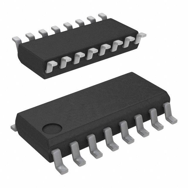
| 描述 | IC LINE DRIVER QUAD CMOS 16-SOIC |
| 产品分类 | |
| 品牌 | Texas Instruments |
| 数据手册 | |
| 产品图片 |
|
| 产品型号 | DS26C31TMX |
| rohs | 含铅 / 不符合限制有害物质指令(RoHS)规范要求 |
| 产品系列 | - |
| 供应商器件封装 | 16-SOIC N |
| 其它名称 | DS26C31TMXCT |
| 包装 | 剪切带 (CT) |
| 协议 | RS422 |
| 双工 | - |
| 安装类型 | 表面贴装 |
| 封装/外壳 | 16-SOIC(0.154",3.90mm 宽) |
| 工作温度 | -40°C ~ 85°C |
| 接收器滞后 | - |
| 数据速率 | - |
| 标准包装 | 1 |
| 电压-电源 | 4.5 V ~ 5.5 V |
| 类型 | 驱动器 |
| 驱动器/接收器数 | 4/0 |


- 商务部:美国ITC正式对集成电路等产品启动337调查
- 曝三星4nm工艺存在良率问题 高通将骁龙8 Gen1或转产台积电
- 太阳诱电将投资9.5亿元在常州建新厂生产MLCC 预计2023年完工
- 英特尔发布欧洲新工厂建设计划 深化IDM 2.0 战略
- 台积电先进制程称霸业界 有大客户加持明年业绩稳了
- 达到5530亿美元!SIA预计今年全球半导体销售额将创下新高
- 英特尔拟将自动驾驶子公司Mobileye上市 估值或超500亿美元
- 三星加码芯片和SET,合并消费电子和移动部门,撤换高东真等 CEO
- 三星电子宣布重大人事变动 还合并消费电子和移动部门
- 海关总署:前11个月进口集成电路产品价值2.52万亿元 增长14.8%


PDF Datasheet 数据手册内容提取
Product Sample & Technical Tools & Support & Folder Buy Documents Software Community DS26C31M,DS26C31T SNLS375C–JUNE1998–REVISEDJANUARY2015 DS26C31x CMOS Quad Tri-State Differential Line Driver 1 Features 3 Description • TTLInputCompatible The DS26C31 device is a quad differential line driver 1 designed for digital data transmission over balanced • TypicalPropagationDelays:6ns lines. The DS26C31T meets all the requirements of • TypicalOutputSkew:0.5ns EIA standard RS-422 while retaining the low power • OutputsWillNotLoadLineWhenV =0V characteristics of CMOS. The DS26C31M is CC compatible with EIA standard RS-422; however, one • DS26C31TMeetstheRequirementsofEIA exception in test methodology is taken(2). This StandardRS-422 enables the construction of serial and terminal • OperationFromSingle5-VSupply interfaces while maintaining minimal power • Tri-StateOutputsforConnectiontoSystemBuses consumption. • LowQuiescentCurrent TheDS26C31acceptsTTLorCMOSinputlevelsand • AvailableinSurfaceMount translates these to RS-422 output levels. This part uses special output circuitry that enables the drivers • Mil-Std-883CCompliant to power down without loading down the bus. This device has enable and disable circuitry common to all 2 Applications four drivers. The DS26C31 is pin compatible to the DifferentialLineDriverforRS-422Applications AM26LS31andtheDS26LS31. All inputs are protected against damage due to electrostaticdischargebydiodestoV andground. CC DeviceInformation(1) PARTNUMBER PACKAGE BODYSIZE(NOM) SNLS3759577 9.90mm×3.91mm DS26C31M PDIP(16) 19.304mm×6.35mm SNLS3759577 9.90mm×3.91mm DS26C31T PDIP(16) 19.304mm×6.35mm (1) For all available packages, see the orderable addendum at theendofthedatasheet. (2) The DS26C31M (−55°C to 125°C) is tested with V OUT between 6 V and 0 V while RS-422A condition is 6 V and −0.25V. 4 Device Logic Diagram 1 An IMPORTANT NOTICE at the end of this data sheet addresses availability, warranty, changes, use in safety-critical applications, intellectualpropertymattersandotherimportantdisclaimers.PRODUCTIONDATA.
DS26C31M,DS26C31T SNLS375C–JUNE1998–REVISEDJANUARY2015 www.ti.com Table of Contents 1 Features.................................................................. 1 9.2 FunctionalBlockDiagram.......................................13 2 Applications........................................................... 1 9.3 FeatureDescription.................................................13 3 Description............................................................. 1 9.4 DeviceFunctionalModes........................................13 4 DeviceLogicDiagram........................................... 1 10 ApplicationandImplementation........................ 14 10.1 ApplicationInformation..........................................14 5 RevisionHistory..................................................... 2 10.2 TypicalApplication................................................14 6 PinConfigurationandFunctions......................... 3 11 PowerSupplyRecommendations..................... 16 7 Specifications......................................................... 4 12 Layout................................................................... 16 7.1 AbsoluteMaximumRatings......................................4 12.1 LayoutGuidelines.................................................16 7.2 RecommendedOperatingConditions.......................4 12.2 LayoutExample....................................................16 7.3 DCElectricalCharacteristics....................................5 13 DeviceandDocumentationSupport................. 17 7.4 SwitchingCharacteristics .........................................6 7.5 ComparisonTableofSwitchingCharacteristicsinto 13.1 RelatedLinks........................................................17 “LS-Type”Load..........................................................6 13.2 Trademarks...........................................................17 7.6 TypicalCharacteristics..............................................7 13.3 ElectrostaticDischargeCaution............................17 8 ParameterMeasurementInformation................11 13.4 Glossary................................................................17 9 DetailedDescription............................................ 13 14 Mechanical,Packaging,andOrderable Information........................................................... 17 9.1 Overview.................................................................13 5 Revision History NOTE:Pagenumbersforpreviousrevisionsmaydifferfrompagenumbersinthecurrentversion. ChangesfromRevisionB(April2013)toRevisionC Page • AddedFeatureDescriptionsection,DeviceFunctionalModes,ApplicationandImplementationsection,Power SupplyRecommendationssection,Layoutsection,DeviceandDocumentationSupportsection,andMechanical, Packaging,andOrderableInformationsection...................................................................................................................... 1 ChangesfromRevisionA(April2013)toRevisionB Page • ChangedlayoutofNationalDataSheettoTIformat............................................................................................................. 9 2 SubmitDocumentationFeedback Copyright©1998–2015,TexasInstrumentsIncorporated ProductFolderLinks:DS26C31M DS26C31T
DS26C31M,DS26C31T www.ti.com SNLS375C–JUNE1998–REVISEDJANUARY2015 6 Pin Configuration and Functions D,NFGPackage 16Pins NAJPackage TopView 20Pins TopView PinFunctions PIN I/O DESCRIPTION NAME NO.(1) DIFFERENTIALSIGNALINGI/O CHANNELA 3,2 O ChannelAinvertingandnon-invertingdifferentialdriveroutputs OUTPUTS(–,+) CHANNELB 5,6 O ChannelBinvertingandnon-invertingdifferentialdriveroutputs OUTPUTS(–,+) CHANNELC 11,10 O ChannelCinvertingandnon-invertingdifferentialdriveroutputs OUTPUTS(–,+) CHANNELD 13,14 O ChannelDinvertingandnon-invertingdifferentialdriveroutputs OUTPUTS(–,+) INPUTA 1 I TTL/CMOScompatibleinputforchannelA INPUTB 7 I TTL/CMOScompatibleinputforchannelB INPUTC 9 I TTL/CMOScompatibleinputforchannelC INPUTD 15 I TTL/CMOScompatibleinputforchannelD CONTROLPINS ENABLE 4 I Logic-highENABLEControl ENABLE 12 I Logic-lowENABLEControl POWER GND 8 — GNDPin VCC 16 — Supplypin,provide5Vsupply (1) PinnumberscorrespondtoPDIPandSOICpackages. Copyright©1998–2015,TexasInstrumentsIncorporated SubmitDocumentationFeedback 3 ProductFolderLinks:DS26C31M DS26C31T
DS26C31M,DS26C31T SNLS375C–JUNE1998–REVISEDJANUARY2015 www.ti.com 7 Specifications 7.1 Absolute Maximum Ratings(1)(2)(3) MIN MAX UNIT SupplyVoltage(V ) −0.5 7 V CC DCInputVoltage(V ) −1.5 V +1.5 V IN CC DCOutputVoltage(V ) −0.5 7 V OUT ClampDiodeCurrent(I ,I ) –20 20 mA IK OK DCOutputCurrent,perpin(I ) –150 150 mA OUT DCV orGNDCurrent,perpin(I ) CC CC MaxPowerDissipation(P )at25°C(4) Ceramic“NFE”package 2419 mW D Plastic“NFG”package 1736 mW SOIC“D”package 1226 mW Ceramic“NAD”package 1182 mW Ceramic“NAJ”package 2134 mW LeadTemperature(T ) (Soldering,4s) 260 °C L StorageTemperature,T −65 150 °C stg (1) StressesbeyondthoselistedunderAbsoluteMaximumRatingsmaycausepermanentdamagetothedevice.Thesearestressratings only,whichdonotimplyfunctionaloperationofthedeviceattheseoranyotherconditionsbeyondthoseindicatedunderRecommended OperatingConditions.Exposuretoabsolute-maximum-ratedconditionsforextendedperiodsmayaffectdevicereliability. (2) Unlessotherwisespecified,allvoltagesarereferencedtoground.Allcurrentsintodevicepinsarepositive,allcurrentsoutofdevice pinsarenegative. (3) IfMilitary/Aerospacespecifieddevicesarerequired,pleasecontacttheTexasInstrumentsSalesOffice/Distributorsforavailabilityand specifications. (4) Ratingsapplytoambienttemperatureat25°C.AbovethistemperaturederateNFGpackageat13.89mW/°C,NFEpackage16.13 mW/°C,Dpackage9.80mW/°C,NAJpackage12.20mW/°C,andNADpackage6.75mW/°C. 7.2 Recommended Operating Conditions MIN MAX UNIT SupplyVoltage(V ) 4.50 5.50 V CC DCInputorOutputVoltage (V ,V ) 0 V V IN OUT CC OperatingTemperatureRange(T ) DS26C31T −40 85 °C A DS26C31M −55 125 °C InputRiseorFallTimes(t,t) 500 ns r f 4 SubmitDocumentationFeedback Copyright©1998–2015,TexasInstrumentsIncorporated ProductFolderLinks:DS26C31M DS26C31T
DS26C31M,DS26C31T www.ti.com SNLS375C–JUNE1998–REVISEDJANUARY2015 7.3 DC Electrical Characteristics V =5V±10%(unlessotherwisespecified)(1) CC PARAMETER TESTCONDITIONS MIN TYP MAX UNIT V HighLevelInputVoltage 2.0 V IH V LowLevelInputVoltage 0.8 V IL V HighLevelOutputVoltage V =V orV , 2.5 3.4 V OH IN IH IL I =−20mA OUT V LowLevelOutputVoltage V =V orV , 0.3 0.5 V OL IN IH IL I =20mA OUT V DifferentialOutputVoltage R =100Ω 2.0 3.1 V T L See(2) |V |−|V | DifferenceInDifferentialOutput R =100Ω 0.4 V T T L See(2) V CommonModeOutputVoltage R =100Ω 1.8 3.0 V OS L See(2) |V −V | DifferenceInCommonMode R =100Ω 0.4 V OS OS L Output See(2) I InputCurrent V =V ,GND,V ,orV ±1.0 μA IN IN CC IH IL I QuiescentSupplyCurrent(3) DS26C31T V =V orGND 200 500 μA CC IN CC I =0μA V =2.4Vor0.5V(3) 0.8 2.0 mA OUT IN DS26C31M V =V orGND 200 500 μA IN CC I =0μA V =2.4Vor0.5V(3) 0.8 2.1 mA OUT IN I TRI-STATEOutputLeakage V =V orGND OZ OUT CC Current ENABLE=V ±0.5 ±5.0 μA IL ENABLE=V IH I OutputShortCircuitCurrent V =V orGND(2)(4) −30 −150 mA SC IN CC I OutputLeakageCurrentPower DS26C31T V =6V 100 μA OFF OUT Off(2) V =0V V =−0.25V −100 μA CC OUT DS26C31M V =6V 100 μA OUT V =0V V =0V(5) −100 μA CC OUT (1) Unlessotherwisespecified,min/maxlimitsapplyacrosstherecommendedoperatingtemperaturerange.AlltypicalsaregivenforV = CC 5VandT =25°C. A (2) SeeEIASpecificationRS-422forexacttestconditions. (3) Measuredperinput.AllotherinputsatV orGND. CC (4) Thisisthecurrentsourcedwhenahighoutputisshortedtoground.Onlyoneoutputatatimeshouldbeshorted. (5) TheDS26C31M(−55°Cto+125°C)istestedwithV between+6Vand0VwhileRS-422Aconditionis+6Vand−0.25V. OUT Copyright©1998–2015,TexasInstrumentsIncorporated SubmitDocumentationFeedback 5 ProductFolderLinks:DS26C31M DS26C31T
DS26C31M,DS26C31T SNLS375C–JUNE1998–REVISEDJANUARY2015 www.ti.com 7.4 Switching Characteristics V =5V±10%,t ≤6ns,t ≤6ns(Figure22,Figure23,Figure24,Figure25)(1) CC r f DS26C31T DS26C31M PARAMETER TESTCONDITIONS MIN TYP UNIT MAX MAX t ,t PropagationDelaysInputtoOutput S1Open 2 6 11 14 ns PLH PHL Skew (2) S1Open 0.5 2.0 3.0 ns t ,t DifferentialOutputRiseAndFall S1Open 6 10 14 ns TLH THL Times t OutputEnableTime S1Closed 11 19 22 ns PZH t OutputEnableTime S1Closed 13 21 28 ns PZL t OutputDisableTime(3) S1Closed 5 9 12 ns PHZ t OutputDisableTime(3) S1Closed 7 11 14 ns PLZ C PowerDissipationCapacitance(4) 50 pF PD C InputCapacitance 6 pF IN (1) Unlessotherwisespecified,min/maxlimitsapplyacrosstherecommendedoperatingtemperaturerange.AlltypicalsaregivenforV = CC 5VandT =25°C. A (2) Skewisdefinedasthedifferenceinpropagationdelaysbetweencomplementaryoutputsatthe50%point. (3) OutputdisabletimeisthedelayfromENABLEorENABLEbeingswitchedtotheoutputtransistorsturningoff.Theactualdisabletimes arelessthanindicatedduetothedelayaddedbytheRCtimeconstantoftheload. (4) C determinesthenoloaddynamicpowerconsumption,P =C V 2f+I V ,andthenoloaddynamiccurrentconsumption,I PD D PD CC CC CC S =C V f+I . PD CC CC 7.5 Comparison Table of Switching Characteristics into “LS-Type” Load V =5V,T =25°C,t ≤6ns,t ≤6ns(Figure23,Figure25,Figure26,Figure27) (1) CC A r f TEST DS26C31T DS26LS31C PARAMETER UNIT CONDITIONS TYP MAX TYP MAX t ,t PropagationDelaysInputtoOutput C =30pF PLH PHL L S1Closed 6 8 10 15 ns S2Closed Skew See(2) C =30pF L S1Closed 0.5 1.0 2.0 6.0 ns S2Closed t ,t DifferentialOutputRiseandFall C =30pF THL TLH L Times S1Closed 4 6 ns S2Closed t OutputDisableTime(3) C =10pF PLZ L S1Closed 6 9 15 35 ns S2Open t OutputDisableTime(3) C =10pF PHZ L S1Open 4 7 15 25 ns S2Closed t OutputEnableTime C =30pF PZL L S1Closed 14 20 20 30 ns S2Open t OutputEnableTime C =30pF PZH L S1Open 11 17 20 30 ns S2Closed (1) Thistableisprovidedforcomparisonpurposesonly.ThevaluesinthistablefortheDS26C31reflecttheperformanceofthedevicebut arenottestedorverified. (2) Skewisdefinedasthedifferenceinpropagationdelaysbetweencomplementaryoutputsatthe50%point. (3) OutputdisabletimeisthedelayfromENABLEorENABLEbeingswitchedtotheoutputtransistorsturningoff.Theactualdisabletimes arelessthanindicatedduetothedelayaddedbytheRCtimeconstantoftheload. 6 SubmitDocumentationFeedback Copyright©1998–2015,TexasInstrumentsIncorporated ProductFolderLinks:DS26C31M DS26C31T
DS26C31M,DS26C31T www.ti.com SNLS375C–JUNE1998–REVISEDJANUARY2015 7.6 Typical Characteristics Figure1.DifferentialPropagationDelayvsTemperature Figure2.DifferentialPropagationDelayvsPowerSupply Voltage Figure3.DifferentialSkewvsTemperature Figure4.DifferentialSkewvsPowerSupplyVoltage Figure5.DifferentialTransitionTimevsTemperature Figure6.DifferentialTransitionTimevsPowerSupply Voltage Copyright©1998–2015,TexasInstrumentsIncorporated SubmitDocumentationFeedback 7 ProductFolderLinks:DS26C31M DS26C31T
DS26C31M,DS26C31T SNLS375C–JUNE1998–REVISEDJANUARY2015 www.ti.com Typical Characteristics (continued) Figure7.ComplementarySkewvsTemperature Figure8.ComplementarySkewvsPowerSupplyVoltage Figure9.DifferentialOutputVoltagevsOutputCurrent Figure10.DifferentialOutputVoltagevsOutputCurrent Figure11.OutputHighVoltagevsOutputHighCurrent Figure12.OutputHighVoltagevsOutputHighCurrent 8 SubmitDocumentationFeedback Copyright©1998–2015,TexasInstrumentsIncorporated ProductFolderLinks:DS26C31M DS26C31T
DS26C31M,DS26C31T www.ti.com SNLS375C–JUNE1998–REVISEDJANUARY2015 Typical Characteristics (continued) Figure13.OutputLowVoltagevsOutputLowCurrent Figure14.OutputLowVoltagevsOutputLowCurrent Figure15.SupplyCurrentvsTemperature Figure16.OutputLowVoltagevsOutputLowCurrent Figure17.OutputLowVoltagevsOutputLowCurrent Figure18.SupplyCurrentvsTemperature Copyright©1998–2015,TexasInstrumentsIncorporated SubmitDocumentationFeedback 9 ProductFolderLinks:DS26C31M DS26C31T
DS26C31M,DS26C31T SNLS375C–JUNE1998–REVISEDJANUARY2015 www.ti.com Typical Characteristics (continued) Figure19.SupplyCurrentvsPowerSupplyVoltage Figure20.OutputShortCircuitCurrentvsTemperature Figure21.OutputShortCircuitCurrentvsPowerSupplyVoltage 10 SubmitDocumentationFeedback Copyright©1998–2015,TexasInstrumentsIncorporated ProductFolderLinks:DS26C31M DS26C31T
DS26C31M,DS26C31T www.ti.com SNLS375C–JUNE1998–REVISEDJANUARY2015 8 Parameter Measurement Information Note:C1=C2=C3=40pF(IncludingProbeandJigCapacitance),R1=R2=50Ω,R3=500Ω. Figure22. ACTestCircuit Figure23. PropagationDelays Figure24. EnableandDisableTimes Inputpulse;f=1MHz,50%;t ≤6ns,t ≤6ns r f Figure25. DifferentialRiseandFallTimes Copyright©1998–2015,TexasInstrumentsIncorporated SubmitDocumentationFeedback 11 ProductFolderLinks:DS26C31M DS26C31T
DS26C31M,DS26C31T SNLS375C–JUNE1998–REVISEDJANUARY2015 www.ti.com Parameter Measurement Information (continued) Figure26. LoadACTestCircuitfor“LS-Type”Load Figure27. EnableandDisableTimesfor “LS-Type”Load 12 SubmitDocumentationFeedback Copyright©1998–2015,TexasInstrumentsIncorporated ProductFolderLinks:DS26C31M DS26C31T
DS26C31M,DS26C31T www.ti.com SNLS375C–JUNE1998–REVISEDJANUARY2015 9 Detailed Description 9.1 Overview The DS26C31 is a quad differential line driver designed for data transmission over balanced cable or printed circuit board traces. The DS26C31M supports a temperature range of -55°C to 125°C, while the DS26C31T supportsatemperaturerangeof-40°Cto85°C. 9.2 Functional Block Diagram DS26C31x CHANNEL INPUT A A OUTPUT CHANNEL INPUT B B OUTPUT CHANNEL INPUT C C OUTPUT CHANNEL INPUT D D OUTPUT _E_N_A_B_L_E_ ENABLE 5.0V VDD GND 0.1(cid:29)F 9.3 Feature Description Each driver converts the TTL or CMOS signal at its input to a pair of complementary differential outputs. The drivers are enabled when the ENABLE control pin is a logic HIGH or when the ENABLE control pin is a logic LOW. 9.4 Device Functional Modes Table1.FunctionTable(1) ENABLE ENABLE INPUT NON-INVERTINGOUTPUT INVERTINGOUTPUT L H X Z Z Allothercombinationsofenableinputs L L H H H L (1) L=Lowlogicstate X=Irrelevant H=Highlogicstate Z=Tri-state(highimpedance) Copyright©1998–2015,TexasInstrumentsIncorporated SubmitDocumentationFeedback 13 ProductFolderLinks:DS26C31M DS26C31T
DS26C31M,DS26C31T SNLS375C–JUNE1998–REVISEDJANUARY2015 www.ti.com 10 Application and Implementation NOTE Information in the following applications sections is not part of the TI component specification, and TI does not warrant its accuracy or completeness. TI’s customers are responsible for determining suitability of components for their purposes. Customers should validateandtesttheirdesignimplementationtoconfirmsystemfunctionality. 10.1 Application Information The DS26C31 is a quad differential line driver designed for applications that require long distance digital data transmission over balanced cables. The DS26C31 can be used in applications that require conversion from TTL or CMOS input levels to differential signal levels, compatible to RS-422. The use of complimentary signaling in a balanced transmission media provides good immunity in the midst of noisy environments or shifts in ground referencepotential. 10.2 Typical Application Figure28depictsatypicalimplementationoftheDS26C31xdeviceinaRS-422application. *R isoptionalalthoughhighlyrecommendedtoreducereflection. T Figure28. Two-WireBalancedSystem,RS-422 10.2.1 DesignRequirements • ApplyTTLorLVCMOSsignaltodriverinputlinesINPUTA-D. • TransmitcomplementaryoutputsatOUTPUTA-D. • Usecontrolled-impedancetransmissionlinessuchasprintedcircuitboardtraces,twisted-pairwiresorparallel wirecable. • Placeaterminatingresistoratthefarendofthedifferentialpair. 10.2.2 DetailedDesignProcedure • ConnectVCCandGNDpinstothepowerandgroundplanesofthePCBwitha0.1-µFbypasscapacitor. • UseTTL/LVCMOSlogiclevelsatINPUTA-D. • Usecontrolled-impedancetransmissionmediaforthedifferentialoutputsignals. • Placeanoptionalterminatingresistoratthefar-endofthedifferentialpairtoavoidreflection. 14 SubmitDocumentationFeedback Copyright©1998–2015,TexasInstrumentsIncorporated ProductFolderLinks:DS26C31M DS26C31T
DS26C31M,DS26C31T www.ti.com SNLS375C–JUNE1998–REVISEDJANUARY2015 Typical Application (continued) 10.2.3 ApplicationCurves Figure29.NoLoadSupplyCurrentvsDataRate Figure30.LoadedSupplyCurrentvsDataRate Copyright©1998–2015,TexasInstrumentsIncorporated SubmitDocumentationFeedback 15 ProductFolderLinks:DS26C31M DS26C31T
DS26C31M,DS26C31T SNLS375C–JUNE1998–REVISEDJANUARY2015 www.ti.com 11 Power Supply Recommendations It is recommended that the supply (VCC) and ground (GND) pins be connected to power planes that are placed in the inner layers of the printed circuit board. A 0.1-µF bypass capacitor should be connect to the VCC pin such thatthecapacitorisascloseaspossibletothedevice. 12 Layout 12.1 Layout Guidelines The output differential signals of the device should be routed on one layer of the board, and clearance should be provided in order to minimize crosstalk between differential pairs that may be running in parallel over a long distance. Additionally, the differential pairs should have a controlled impedance with minimum impedance discontinuities and be terminated at the far-end, near the receiver, with a resistor that is closely matched to the differential pair impedance in order to minimize transmission line reflections. The differential pairs should be routedwithuniformtracewidthandspacingtominimizeimpedancemismatching. 12.2 Layout Example Via to VCC Via to GND Plane Plane Input 1 16 Bypass Capacitor Input 2 15 TX Differential Pair 3 14 TX Differential Pair Enable 4 13 DS26C31M/DS26C31T Enable 5 12 TX Differential Pair 6 11 TX Differential Pair Input 7 10 Input 8 9 Via to GND Plane Figure31. DS26C31ExampleLayout 16 SubmitDocumentationFeedback Copyright©1998–2015,TexasInstrumentsIncorporated ProductFolderLinks:DS26C31M DS26C31T
DS26C31M,DS26C31T www.ti.com SNLS375C–JUNE1998–REVISEDJANUARY2015 13 Device and Documentation Support 13.1 Related Links The table below lists quick access links. Categories include technical documents, support and community resources,toolsandsoftware,andquickaccesstosampleorbuy. Table2.RelatedLinks TECHNICAL TOOLS& SUPPORT& PARTS PRODUCTFOLDER SAMPLE&BUY DOCUMENTS SOFTWARE COMMUNITY DS26C31M Clickhere Clickhere Clickhere Clickhere Clickhere DS26C31T Clickhere Clickhere Clickhere Clickhere Clickhere 13.2 Trademarks Alltrademarksarethepropertyoftheirrespectiveowners. 13.3 Electrostatic Discharge Caution Thesedeviceshavelimitedbuilt-inESDprotection.Theleadsshouldbeshortedtogetherorthedeviceplacedinconductivefoam duringstorageorhandlingtopreventelectrostaticdamagetotheMOSgates. 13.4 Glossary SLYZ022—TIGlossary. Thisglossarylistsandexplainsterms,acronyms,anddefinitions. 14 Mechanical, Packaging, and Orderable Information The following pages include mechanical, packaging, and orderable information. This information is the most current data available for the designated devices. This data is subject to change without notice and revision of thisdocument.Forbrowser-basedversionsofthisdatasheet,refertotheleft-handnavigation. Copyright©1998–2015,TexasInstrumentsIncorporated SubmitDocumentationFeedback 17 ProductFolderLinks:DS26C31M DS26C31T
PACKAGE OPTION ADDENDUM www.ti.com 14-Nov-2017 PACKAGING INFORMATION Orderable Device Status Package Type Package Pins Package Eco Plan Lead/Ball Finish MSL Peak Temp Op Temp (°C) Device Marking Samples (1) Drawing Qty (2) (6) (3) (4/5) DS26C31TM LIFEBUY SOIC D 16 48 TBD Call TI Call TI -40 to 85 DS26C31TM DS26C31TM/NOPB ACTIVE SOIC D 16 48 Green (RoHS CU SN Level-1-260C-UNLIM -40 to 85 DS26C31TM & no Sb/Br) DS26C31TMX LIFEBUY SOIC D 16 2500 TBD Call TI Call TI -40 to 85 DS26C31TM DS26C31TMX/NOPB ACTIVE SOIC D 16 2500 Green (RoHS CU SN Level-1-260C-UNLIM -40 to 85 DS26C31TM & no Sb/Br) DS26C31TN LIFEBUY PDIP NFG 16 25 TBD Call TI Call TI -40 to 85 DS26C31TN DS26C31TN/NOPB LIFEBUY PDIP NFG 16 25 Green (RoHS CU SN Level-1-NA-UNLIM -40 to 85 DS26C31TN & no Sb/Br) (1) The marketing status values are defined as follows: ACTIVE: Product device recommended for new designs. LIFEBUY: TI has announced that the device will be discontinued, and a lifetime-buy period is in effect. NRND: Not recommended for new designs. Device is in production to support existing customers, but TI does not recommend using this part in a new design. PREVIEW: Device has been announced but is not in production. Samples may or may not be available. OBSOLETE: TI has discontinued the production of the device. (2) RoHS: TI defines "RoHS" to mean semiconductor products that are compliant with the current EU RoHS requirements for all 10 RoHS substances, including the requirement that RoHS substance do not exceed 0.1% by weight in homogeneous materials. Where designed to be soldered at high temperatures, "RoHS" products are suitable for use in specified lead-free processes. TI may reference these types of products as "Pb-Free". RoHS Exempt: TI defines "RoHS Exempt" to mean products that contain lead but are compliant with EU RoHS pursuant to a specific EU RoHS exemption. Green: TI defines "Green" to mean the content of Chlorine (Cl) and Bromine (Br) based flame retardants meet JS709B low halogen requirements of <=1000ppm threshold. Antimony trioxide based flame retardants must also meet the <=1000ppm threshold requirement. (3) MSL, Peak Temp. - The Moisture Sensitivity Level rating according to the JEDEC industry standard classifications, and peak solder temperature. (4) There may be additional marking, which relates to the logo, the lot trace code information, or the environmental category on the device. (5) Multiple Device Markings will be inside parentheses. Only one Device Marking contained in parentheses and separated by a "~" will appear on a device. If a line is indented then it is a continuation of the previous line and the two combined represent the entire Device Marking for that device. (6) Lead/Ball Finish - Orderable Devices may have multiple material finish options. Finish options are separated by a vertical ruled line. Lead/Ball Finish values may wrap to two lines if the finish value exceeds the maximum column width. Addendum-Page 1
PACKAGE OPTION ADDENDUM www.ti.com 14-Nov-2017 Important Information and Disclaimer:The information provided on this page represents TI's knowledge and belief as of the date that it is provided. TI bases its knowledge and belief on information provided by third parties, and makes no representation or warranty as to the accuracy of such information. Efforts are underway to better integrate information from third parties. TI has taken and continues to take reasonable steps to provide representative and accurate information but may not have conducted destructive testing or chemical analysis on incoming materials and chemicals. TI and TI suppliers consider certain information to be proprietary, and thus CAS numbers and other limited information may not be available for release. In no event shall TI's liability arising out of such information exceed the total purchase price of the TI part(s) at issue in this document sold by TI to Customer on an annual basis. Addendum-Page 2
PACKAGE MATERIALS INFORMATION www.ti.com 10-Aug-2018 TAPE AND REEL INFORMATION *Alldimensionsarenominal Device Package Package Pins SPQ Reel Reel A0 B0 K0 P1 W Pin1 Type Drawing Diameter Width (mm) (mm) (mm) (mm) (mm) Quadrant (mm) W1(mm) DS26C31TMX/NOPB SOIC D 16 2500 330.0 16.4 6.5 10.3 2.3 8.0 16.0 Q1 PackMaterials-Page1
PACKAGE MATERIALS INFORMATION www.ti.com 10-Aug-2018 *Alldimensionsarenominal Device PackageType PackageDrawing Pins SPQ Length(mm) Width(mm) Height(mm) DS26C31TMX/NOPB SOIC D 16 2500 367.0 367.0 35.0 PackMaterials-Page2
None
MECHANICAL DATA N0016E N16E (Rev G) www.ti.com
IMPORTANTNOTICE TexasInstrumentsIncorporated(TI)reservestherighttomakecorrections,enhancements,improvementsandotherchangestoits semiconductorproductsandservicesperJESD46,latestissue,andtodiscontinueanyproductorserviceperJESD48,latestissue.Buyers shouldobtainthelatestrelevantinformationbeforeplacingordersandshouldverifythatsuchinformationiscurrentandcomplete. TI’spublishedtermsofsaleforsemiconductorproducts(http://www.ti.com/sc/docs/stdterms.htm)applytothesaleofpackagedintegrated circuitproductsthatTIhasqualifiedandreleasedtomarket.AdditionaltermsmayapplytotheuseorsaleofothertypesofTIproductsand services. ReproductionofsignificantportionsofTIinformationinTIdatasheetsispermissibleonlyifreproductioniswithoutalterationandis accompaniedbyallassociatedwarranties,conditions,limitations,andnotices.TIisnotresponsibleorliableforsuchreproduced documentation.Informationofthirdpartiesmaybesubjecttoadditionalrestrictions.ResaleofTIproductsorserviceswithstatements differentfromorbeyondtheparametersstatedbyTIforthatproductorservicevoidsallexpressandanyimpliedwarrantiesforthe associatedTIproductorserviceandisanunfairanddeceptivebusinesspractice.TIisnotresponsibleorliableforanysuchstatements. BuyersandotherswhoaredevelopingsystemsthatincorporateTIproducts(collectively,“Designers”)understandandagreethatDesigners remainresponsibleforusingtheirindependentanalysis,evaluationandjudgmentindesigningtheirapplicationsandthatDesignershave fullandexclusiveresponsibilitytoassurethesafetyofDesigners'applicationsandcomplianceoftheirapplications(andofallTIproducts usedinorforDesigners’applications)withallapplicableregulations,lawsandotherapplicablerequirements.Designerrepresentsthat,with respecttotheirapplications,Designerhasallthenecessaryexpertisetocreateandimplementsafeguardsthat(1)anticipatedangerous consequencesoffailures,(2)monitorfailuresandtheirconsequences,and(3)lessenthelikelihoodoffailuresthatmightcauseharmand takeappropriateactions.DesigneragreesthatpriortousingordistributinganyapplicationsthatincludeTIproducts,Designerwill thoroughlytestsuchapplicationsandthefunctionalityofsuchTIproductsasusedinsuchapplications. TI’sprovisionoftechnical,applicationorotherdesignadvice,qualitycharacterization,reliabilitydataorotherservicesorinformation, including,butnotlimitedto,referencedesignsandmaterialsrelatingtoevaluationmodules,(collectively,“TIResources”)areintendedto assistdesignerswhoaredevelopingapplicationsthatincorporateTIproducts;bydownloading,accessingorusingTIResourcesinany way,Designer(individuallyor,ifDesignerisactingonbehalfofacompany,Designer’scompany)agreestouseanyparticularTIResource solelyforthispurposeandsubjecttothetermsofthisNotice. TI’sprovisionofTIResourcesdoesnotexpandorotherwisealterTI’sapplicablepublishedwarrantiesorwarrantydisclaimersforTI products,andnoadditionalobligationsorliabilitiesarisefromTIprovidingsuchTIResources.TIreservestherighttomakecorrections, enhancements,improvementsandotherchangestoitsTIResources.TIhasnotconductedanytestingotherthanthatspecifically describedinthepublisheddocumentationforaparticularTIResource. Designerisauthorizedtouse,copyandmodifyanyindividualTIResourceonlyinconnectionwiththedevelopmentofapplicationsthat includetheTIproduct(s)identifiedinsuchTIResource.NOOTHERLICENSE,EXPRESSORIMPLIED,BYESTOPPELOROTHERWISE TOANYOTHERTIINTELLECTUALPROPERTYRIGHT,ANDNOLICENSETOANYTECHNOLOGYORINTELLECTUALPROPERTY RIGHTOFTIORANYTHIRDPARTYISGRANTEDHEREIN,includingbutnotlimitedtoanypatentright,copyright,maskworkright,or otherintellectualpropertyrightrelatingtoanycombination,machine,orprocessinwhichTIproductsorservicesareused.Information regardingorreferencingthird-partyproductsorservicesdoesnotconstitutealicensetousesuchproductsorservices,orawarrantyor endorsementthereof.UseofTIResourcesmayrequirealicensefromathirdpartyunderthepatentsorotherintellectualpropertyofthe thirdparty,oralicensefromTIunderthepatentsorotherintellectualpropertyofTI. TIRESOURCESAREPROVIDED“ASIS”ANDWITHALLFAULTS.TIDISCLAIMSALLOTHERWARRANTIESOR REPRESENTATIONS,EXPRESSORIMPLIED,REGARDINGRESOURCESORUSETHEREOF,INCLUDINGBUTNOTLIMITEDTO ACCURACYORCOMPLETENESS,TITLE,ANYEPIDEMICFAILUREWARRANTYANDANYIMPLIEDWARRANTIESOF MERCHANTABILITY,FITNESSFORAPARTICULARPURPOSE,ANDNON-INFRINGEMENTOFANYTHIRDPARTYINTELLECTUAL PROPERTYRIGHTS.TISHALLNOTBELIABLEFORANDSHALLNOTDEFENDORINDEMNIFYDESIGNERAGAINSTANYCLAIM, INCLUDINGBUTNOTLIMITEDTOANYINFRINGEMENTCLAIMTHATRELATESTOORISBASEDONANYCOMBINATIONOF PRODUCTSEVENIFDESCRIBEDINTIRESOURCESOROTHERWISE.INNOEVENTSHALLTIBELIABLEFORANYACTUAL, DIRECT,SPECIAL,COLLATERAL,INDIRECT,PUNITIVE,INCIDENTAL,CONSEQUENTIALOREXEMPLARYDAMAGESIN CONNECTIONWITHORARISINGOUTOFTIRESOURCESORUSETHEREOF,ANDREGARDLESSOFWHETHERTIHASBEEN ADVISEDOFTHEPOSSIBILITYOFSUCHDAMAGES. UnlessTIhasexplicitlydesignatedanindividualproductasmeetingtherequirementsofaparticularindustrystandard(e.g.,ISO/TS16949 andISO26262),TIisnotresponsibleforanyfailuretomeetsuchindustrystandardrequirements. WhereTIspecificallypromotesproductsasfacilitatingfunctionalsafetyorascompliantwithindustryfunctionalsafetystandards,such productsareintendedtohelpenablecustomerstodesignandcreatetheirownapplicationsthatmeetapplicablefunctionalsafetystandards andrequirements.Usingproductsinanapplicationdoesnotbyitselfestablishanysafetyfeaturesintheapplication.Designersmust ensurecompliancewithsafety-relatedrequirementsandstandardsapplicabletotheirapplications.DesignermaynotuseanyTIproductsin life-criticalmedicalequipmentunlessauthorizedofficersofthepartieshaveexecutedaspecialcontractspecificallygoverningsuchuse. Life-criticalmedicalequipmentismedicalequipmentwherefailureofsuchequipmentwouldcauseseriousbodilyinjuryordeath(e.g.,life support,pacemakers,defibrillators,heartpumps,neurostimulators,andimplantables).Suchequipmentincludes,withoutlimitation,all medicaldevicesidentifiedbytheU.S.FoodandDrugAdministrationasClassIIIdevicesandequivalentclassificationsoutsidetheU.S. TImayexpresslydesignatecertainproductsascompletingaparticularqualification(e.g.,Q100,MilitaryGrade,orEnhancedProduct). Designersagreethatithasthenecessaryexpertisetoselecttheproductwiththeappropriatequalificationdesignationfortheirapplications andthatproperproductselectionisatDesigners’ownrisk.Designersaresolelyresponsibleforcompliancewithalllegalandregulatory requirementsinconnectionwithsuchselection. DesignerwillfullyindemnifyTIanditsrepresentativesagainstanydamages,costs,losses,and/orliabilitiesarisingoutofDesigner’snon- compliancewiththetermsandprovisionsofthisNotice. MailingAddress:TexasInstruments,PostOfficeBox655303,Dallas,Texas75265 Copyright©2018,TexasInstrumentsIncorporated