ICGOO在线商城 > 集成电路(IC) > 接口 - 驱动器,接收器,收发器 > KSZ9031RNXIA
 Datasheet下载
- 型号: KSZ9031RNXIA
- 制造商: Micrel
- 库位|库存: xxxx|xxxx
- 要求:
| 数量阶梯 | 香港交货 | 国内含税 |
| +xxxx | $xxxx | ¥xxxx |
查看当月历史价格
查看今年历史价格
KSZ9031RNXIA产品简介:
ICGOO电子元器件商城为您提供KSZ9031RNXIA由Micrel设计生产,在icgoo商城现货销售,并且可以通过原厂、代理商等渠道进行代购。 KSZ9031RNXIA价格参考¥询价-¥询价。MicrelKSZ9031RNXIA封装/规格:接口 - 驱动器,接收器,收发器, 全 收发器 4/4 以太网 48-QFN(7x7)。您可以下载KSZ9031RNXIA参考资料、Datasheet数据手册功能说明书,资料中有KSZ9031RNXIA 详细功能的应用电路图电压和使用方法及教程。
Microchip Technology的KSZ9031RNXIA是一款高性能的千兆以太网PHY(物理层)收发器,广泛应用于各种需要高速网络连接的场景。以下是其主要应用场景:

 1. 工业自动化
在工业自动化领域,KSZ9031RNXIA可以用于构建可靠的工业以太网网络,支持实时数据传输和控制信号的快速响应。它适用于工厂自动化、过程控制、智能电网等场景,确保设备之间的高效通信。

 2. 嵌入式系统
该芯片常用于嵌入式系统的开发中,特别是在需要集成千兆以太网接口的设备上。例如,智能家居控制器、物联网(IoT)网关、工业计算机等。通过集成KSZ9031RNXIA,这些设备可以获得稳定的网络连接,支持远程管理和数据传输。

 3. 网络设备
在网络设备如路由器、交换机、无线接入点等中,KSZ9031RNXIA提供了强大的千兆以太网功能,确保数据的高速传输和低延迟。它支持多种标准协议,如IEEE 802.3ab(1000BASE-T),并具备优异的EMI性能,适用于对电磁干扰敏感的环境。

 4. 汽车电子
随着汽车智能化的发展,车载网络的需求不断增加。KSZ9031RNXIA可用于汽车中的以太网通信模块,支持ADAS(高级驾驶辅助系统)、信息娱乐系统、车联网等功能。它符合AEC-Q100标准,具备高可靠性和抗干扰能力,适合严苛的汽车环境。

 5. 服务器与存储设备
在数据中心和企业级服务器中,KSZ9031RNXIA可以作为网络接口卡(NIC)的一部分,提供高效的千兆以太网连接。它支持节能模式,能够在低负载时减少功耗,同时保持高性能的数据传输能力。

 6. 安全监控
在安防监控系统中,KSZ9031RNXIA可用于高清摄像头、视频编码器等设备,确保视频流的稳定传输。它支持PoE(以太网供电)功能,简化了安装和布线,降低了部署成本。

总之,KSZ9031RNXIA凭借其高性能、低功耗和广泛的兼容性,成为众多需要高速网络连接应用的理想选择。
| 参数 | 数值 |
| 产品目录 | 集成电路 (IC)半导体 |
| 描述 | IC TXRX ETHERNET 48-QFN以太网 IC 1-Port GigabitEthrnt Ethernet PHY |
| 产品分类 | |
| 品牌 | Micrel |
| 产品手册 | |
| 产品图片 |
|
| rohs | 符合RoHS无铅 / 符合限制有害物质指令(RoHS)规范要求 |
| 产品系列 | 通信及网络 IC,以太网 IC,Micrel KSZ9031RNXIA- |
| 数据手册 | |
| 产品型号 | KSZ9031RNXIA |
| 产品 | Ethernet Transceivers |
| 产品种类 | 以太网 IC |
| 以太网连接类型 | 10Base-T, 100Base-TX, 1000Base-T |
| 供应商器件封装 | 48-QFN(7x7) |
| 其它名称 | 576-4346 |
| 包装 | 托盘 |
| 协议 | 以太网 |
| 双工 | 全 |
| 商标 | Micrel |
| 安装类型 | 表面贴装 |
| 安装风格 | SMD/SMT |
| 封装 | Tray |
| 封装/外壳 | 48-VFQFN 裸露焊盘 |
| 封装/箱体 | QFN-48 |
| 工作温度 | -40°C ~ 85°C |
| 工厂包装数量 | 260 |
| 接收器滞后 | - |
| 支持标准 | 802.3 |
| 收发器数量 | 1 Transceiver |
| 数据速率 | 10 Mbps, 100 Mbps, 1000 Mbps |
| 最大工作温度 | + 85 C |
| 最大电源电流 | 221 mA |
| 最小工作温度 | - 40 C |
| 标准包装 | 260 |
| 特色产品 | http://www.digikey.com/product-highlights/cn/zh/micrel-ksz9031-series-ethernet-transceiver/3904 |
| 电压-电源 | 1.8V,2.5V,3.3V |
| 电源电压-最大 | 3.465 V |
| 电源电压-最小 | 1.14 V |
| 类型 | Ethernet Transceivers |
| 系列 | KSZ9031 |
| 驱动器/接收器数 | 4/4 |


- 商务部:美国ITC正式对集成电路等产品启动337调查
- 曝三星4nm工艺存在良率问题 高通将骁龙8 Gen1或转产台积电
- 太阳诱电将投资9.5亿元在常州建新厂生产MLCC 预计2023年完工
- 英特尔发布欧洲新工厂建设计划 深化IDM 2.0 战略
- 台积电先进制程称霸业界 有大客户加持明年业绩稳了
- 达到5530亿美元!SIA预计今年全球半导体销售额将创下新高
- 英特尔拟将自动驾驶子公司Mobileye上市 估值或超500亿美元
- 三星加码芯片和SET,合并消费电子和移动部门,撤换高东真等 CEO
- 三星电子宣布重大人事变动 还合并消费电子和移动部门
- 海关总署:前11个月进口集成电路产品价值2.52万亿元 增长14.8%


PDF Datasheet 数据手册内容提取
KSZ9031RNX Gigabit Ethernet Transceiver with RGMII Support Features • Single-Chip 10/100/1000Mbps Ethernet Trans- • Operating Voltages ceiver Suitable for IEEE 802.3 Applications - Core (DVDDL, AVDDL, AVDDL_PLL): 1.2V • RGMII Timing Supports On-Chip Delay According (External FET or Regulator) to RGMII Version 2.0, with Programming Options - VDD I/O (DVDDH): 3.3V, 2.5V, or 1.8V for External Delay and Making Adjustments and - Transceiver (AVDDH): 3.3V or 2.5V (Com- Corrections to TX and RX Timing Paths mercial Temp.) • RGMII with 3.3V/2.5V/1.8V Tolerant I/Os • AEC-Q100 Grade 3 (KSZ9031RNXUA/UB) and • Auto-Negotiation to Automatically Select the Grade 2 (KSZ9031RNXVA/VB) Qualified for Auto- Highest Link-Up Speed (10/100/1000Mbps) and motive Applications Duplex (Half/Full) • 48-pin QFN (7mm × 7mm) Package • On-Chip Termination Resistors for the Differential Pairs Target Applications • On-Chip LDO Controller to Support Single 3.3V Supply Operation – Requires Only One External • Laser/Network Printer FET to Generate 1.2V for the Core • Network Attached Storage (NAS) • Jumbo Frame Support up to 16 KB • Network Server • 125MHz Reference Clock Output • Gigabit LAN on Motherboard (GLOM) • Energy Detect Power-Down Mode for Reduced • Broadband Gateway Power Consumption When the Cable is Not • Gigabit SOHO/SMB Router Attached • IPTV • Wake-On-LAN (WOL) Support with Robust Cus- • IP Set-Top Box tom-Packet Detection • Game Console • Programmable LED Outputs for Link, Activity, and • Triple-Play (Data, Voice, Video) Media Center Speed • Industrial Control • Baseline Wander Correction • Automotive In-Vehicle Networking • LinkMD TDR-Based Cable Diagnostic to Identify Faulty Copper Cabling • Parametric NAND Tree Support to Detect Faults Between Chip I/Os and Board • Loopback Modes for Diagnostics • Automatic MDI/MDI-X Crossover to Detect and Correct Pair Swap at all Speeds of Operation • Automatic Detection and Correction of Pair Swaps, Pair Skew, and Pair Polarity • MDC/MDIO Management Interface for PHY Reg- ister Configuration • Interrupt Pin Option • Power-Down and Power-Saving Modes 2016-2017 Microchip Technology Inc. DS00002117F-page 1
KSZ9031RNX TO OUR VALUED CUSTOMERS It is our intention to provide our valued customers with the best documentation possible to ensure successful use of your Microchip products. To this end, we will continue to improve our publications to better suit your needs. Our publications will be refined and enhanced as new volumes and updates are introduced. If you have any questions or comments regarding this publication, please contact the Marketing Communications Department via E-mail at docerrors@microchip.com. We welcome your feedback. Most Current Data Sheet To obtain the most up-to-date version of this data sheet, please register at our Worldwide Web site at: http://www.microchip.com You can determine the version of a data sheet by examining its literature number found on the bottom outside corner of any page. The last character of the literature number is the version number, (e.g., DS30000000A is version A of document DS30000000). Errata An errata sheet, describing minor operational differences from the data sheet and recommended workarounds, may exist for cur- rent devices. As device/documentation issues become known to us, we will publish an errata sheet. The errata will specify the revision of silicon and revision of document to which it applies. To determine if an errata sheet exists for a particular device, please check with one of the following: • Microchip’s Worldwide Web site; http://www.microchip.com • Your local Microchip sales office (see last page) When contacting a sales office, please specify which device, revision of silicon and data sheet (include -literature number) you are using. Customer Notification System Register on our web site at www.microchip.com to receive the most current information on all of our products. DS00002117F-page 2 2016-2017 Microchip Technology Inc.
KSZ9031RNX Table of Contents 1.0 Introduction .....................................................................................................................................................................................4 2.0 Pin Description and Configuration ..................................................................................................................................................5 3.0 Functional Description ..................................................................................................................................................................13 4.0 Register Descriptions ....................................................................................................................................................................31 5.0 Operational Characteristics ...........................................................................................................................................................52 6.0 Electrical Characteristics ...............................................................................................................................................................53 7.0 Timing Diagrams ...........................................................................................................................................................................57 8.0 Reset Circuit .................................................................................................................................................................................63 9.0 Reference Circuits — LED Strap-In Pins ......................................................................................................................................65 10.0 Reference Clock - Connection and Selection .............................................................................................................................66 11.0 On-Chip LDO Controller - MOSFET Selection ............................................................................................................................66 12.0 Magnetic - Connection and Selection .........................................................................................................................................67 13.0 Package Outlines ........................................................................................................................................................................69 Appendix A: Data Sheet Revision History ...........................................................................................................................................74 The Microchip Web Site ......................................................................................................................................................................76 Customer Change Notification Service ...............................................................................................................................................76 Customer Support ...............................................................................................................................................................................76 Product Identification System .............................................................................................................................................................77 2016-2017 Microchip Technology Inc. DS00002117F-page 3
KSZ9031RNX 1.0 INTRODUCTION 1.1 General Description The KSZ9031RNX is a completely integrated triple-speed (10BASE-T/100BASE-TX/1000BASE-T) Ethernet physical- layer transceiver for transmission and reception of data on standard CAT-5 unshielded twisted pair (UTP) cable. The KSZ9031RNX provides the Reduced Gigabit Media Independent Interface (RGMII) for direct connection to RGMII MACs in Gigabit Ethernet processors and switches for data transfer at 10/100/1000 Mbps. The KSZ9031RNX reduces board cost and simplifies board layout by using on-chip termination resistors for the four differential pairs and by integrating an LDO controller to drive a low-cost MOSFET to supply the 1.2V core. The KSZ9031RNX offers diagnostic features to facilitate system bring-up and debugging in production testing and in product deployment. Parametric NAND tree support enables fault detection between KSZ9031 I/Os and the board. The LinkMD® TDR-based cable diagnostic identifies faulty copper cabling. Remote and local loopback functions verify ana- log and digital data paths. The standard KSZ9031RNX is available in a 48-pin, lead-free QFN package, and the AEC-Q100 automotive qualified parts, KSZ9031RNXUA/UB and KSZ9031RNXVA/VB, are available in a 48-pin lead-free VQFN (wettable) package. FIGURE 1-1: SYSTEM BLOCK DIAGRAM N 1E0T/H10E0RR/G1N0ME0TI0I MMbApCs MAMNDRACGG/MMEIMDIIEONT KSZ9031RNX P TERMINATIOESISTORS GNETICS CONRNJE-4C5TOR M 111E000DB00IB0aABsa Tesa-eYsT-ePT-ETXS HIR A C M N- O LDO PME_N CONTROLLER VIN VOUT 3.3VA 1.2V (FOR CORE VOLTAGES) (SYSTEM POWER CIRCUIT) 2016-2017 Microchip Technology Inc. DS00002117F-page 4
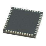
KSZ9031RNX 2.0 PIN DESCRIPTION AND CONFIGURATION FIGURE 2-1: 48-QFN PIN ASSIGNMENT (TOP VIEW) O/ ISET NC XI XO AVDDL_PLL LDO_O RESET_N CLK125_NDLED_MODE DVDDH DVDDL INT_N/PME_N2 MDIO 48 47 46 45 44 43 42 41 40 39 38 37 AVDDH 1 36 MDC RX_CLK/ TXRXP_A 2 35 PHYAD2 TXRXM_A 3 34 DVDDH RX_DV/ AVDDL 4 33 CLK125_EN RXD0/ TXRXP_B 5 32 MODE0 KSZ9031RNX RXD1/ TXRXM_B 6 31 MODE1 PADDLE GROUND TXRXP_C 7 30 DVDDL (ON BOTTOM OF CHIP) TXRXM_C 8 29 VSS AVDDL 9 28 RXD2/ MODE2 TXRXP_D 10 27 RXD3/ MODE3 TXRXM_D 11 26 DVDDL AVDDH 12 25 TX_EN 13 14 15 16 17 18 19 20 21 22 23 24 NC DVDDL LED2/PHYAD1 DVHDD LED1 / PME_N1 / PHYAD0 DVDDL TXD0 TXD1 TXD2 TXD3 DVDDL GTX_CLK 2016-2017 Microchip Technology Inc. DS00002117F-page 5
KSZ9031RNX TABLE 2-1: SIGNALS - KSZ9031RNX Type Pin Pin Note Description Number Name 2-1 1 AVDDH P 3.3V/2.5V (commercial temp only) analog V DD Media Dependent Interface[0], positive signal of differential pair 1000BASE-T mode: TXRXP_A corresponds to BI_DA+ for MDI configuration and BI_DB+ for MDI- 2 TXRXP_A I/O X configuration, respectively. 10BASE-T/100BASE-TX mode: TXRXP_A is the positive transmit signal (TX+) for MDI configuration and the positive receive signal (RX+) for MDI-X configuration, respectively. Media Dependent Interface[0], negative signal of differential pair 1000BASE-T mode: TXRXM_A corresponds to BI_DA– for MDI configuration and BI_DB– for 3 TXRXM_A I/O MDI-X configuration, respectively. 10BASE-T/100BASE-TX mode: TXRXM_A is the negative transmit signal (TX–) for MDI configuration and the negative receive signal (RX–) for MDI-X configuration, respectively. 4 AVDDL P 1.2V analog V DD Media Dependent Interface[1], positive signal of differential pair 1000BASE-T mode: TXRXP_B corresponds to BI_DB+ for MDI configuration and BI_DA+ for MDI- 5 TXRXP_B I/O X configuration, respectively. 10BASE-T/100BASE-TX mode: TXRXP_B is the positive receive signal (RX+) for MDI configuration and the positive transmit signal (TX+) for MDI-X configuration, respectively. Media Dependent Interface[1], negative signal of differential pair 1000BASE-T mode: TXRXM_B corresponds to BI_DB– for MDI configuration and BI_DA– for 6 TXRXM_B I/O MDI-X configuration, respectively. 10BASE-T/100BASE-TX mode: TXRXM_B is the negative receive signal (RX–) for MDI configuration and the negative transmit signal (TX–) for MDI-X configuration, respectively. Media Dependent Interface[2], positive signal of differential pair 1000BASE-T mode: TXRXP_C corresponds to BI_DC+ for MDI configuration and BI_DD+ for 7 TXRXP_C I/O MDI-X configuration, respectively. 10BASE-T/100BASE-TX mode: TXRXP_C is not used. Media Dependent Interface[2], negative signal of differential pair 1000BASE-T mode: TXRXM_C corresponds to BI_DC– for MDI configuration and BI_DD– for 8 TXRXM_C I/O MDI-X configuration, respectively. 10BASE-T/100BASE-TX mode: TXRXM_C is not used. 9 AVDDL P 1.2V analog V DD DS00002117F-page 6 2016-2017 Microchip Technology Inc.
KSZ9031RNX TABLE 2-1: SIGNALS - KSZ9031RNX (CONTINUED) Type Pin Pin Note Description Number Name 2-1 Media Dependent Interface[3], positive signal of differential pair 1000BASE-T mode: TXRXP_D corresponds to BI_DD+ for MDI configuration and BI_DC+ for 10 TXRXP_D I/O MDI-X configuration, respectively. 10BASE-T/100BASE-TX mode: TXRXP_D is not used. Media Dependent Interface[3], negative signal of differential pair 1000BASE-T mode: TXRXM_D corresponds to BI_DD– for MDI configuration and BI_DC– for 11 TXRXM_D I/O MDI-X configuration, respectively. 10BASE-T/100BASE-TX mode: TXRXM_D is not used. 12 AVDDH P 3.3V/2.5V (commercial temp only) analog V DD No connect. This pin is not bonded and can be connected to digital ground for 13 NC — footprint compatibility with the KSZ9021RN Gigabit PHY. 14 DVDDL P 1.2V digital V DD 2016-2017 Microchip Technology Inc. DS00002117F-page 7
KSZ9031RNX TABLE 2-1: SIGNALS - KSZ9031RNX (CONTINUED) Type Pin Pin Note Description Number Name 2-1 LED output: Programmable LED2 output Config mode: The pull-up/pull-down value is latched as PHYAD[1] during power-up/reset. See the Strap-In Options - KSZ9031RNX section for details. The LED2 pin is programmed by the LED_MODE strapping option (Pin 41), and is defined as follows: Single-LED Mode Link Pin State LED Definition Link Off H OFF Link On (any speed) L ON Tri-Color Dual-LED Mode Pin State LED Definition Link/Activity LED2 LED1 LED2 LED1 LED2/ 15 I/O PHYAD1 Link Off H H OFF OFF 1000 Link/No Activity L H ON OFF 1000 Link/Activity Toggle H Blinking OFF (RX, TX) 100 Link/No Activity H L OFF ON 100 Link/Activity H Toggle OFF Blinking (RX, TX) 10 Link/No Activity L L ON ON 10 Link/Activity Toggle Toggle Blinking Blinking (RX, TX) For tri-color dual-LED mode, LED2 works in conjunction with LED1 (Pin 17) to indicate 10 Mbps link and activity. 16 DVDDH P 3.3V, 2.5V, or 1.8V digital V DD_I/O DS00002117F-page 8 2016-2017 Microchip Technology Inc.
KSZ9031RNX TABLE 2-1: SIGNALS - KSZ9031RNX (CONTINUED) Type Pin Pin Note Description Number Name 2-1 LED1 output: Programmable LED1 output Config mode: The voltage on this pin is sampled and latched during the power-up/reset process to determine the value of PHYAD[0]. See the Strap-In Options - KSZ9031RNX section for details. PME_N output: Programmable PME_N output (pin option 1). This pin function requires an external pull-up resistor to DVDDH (digital V ) in a range DD_I/O from 1.0 kΩ to 4.7 kΩ. When asserted low, this pin signals that a WOL event has occurred. This pin is not an open-drain for all operating modes. The LED1 pin is programmed by the LED_MODE strapping option (Pin 41), and is defined as follows: Single-LED Mode Activity Pin State LED Definition No Activity H OFF Activity (RX, TX) Toggle Blinking Tri-Color Dual-LED Mode LED1/ 17 PHYAD0/ I/O Pin State LED Definition PME_N1 Link/Activity LED2 LED1 LED2 LED1 Link Off H H OFF OFF 1000 Link/No Activity L H ON OFF 1000 Link/Activity Toggle H Blinking OFF (RX, TX) 100 Link/No Activity H L OFF ON 100 Link/Activity H Toggle OFF Blinking (RX, TX) 10 Link/No Activity L L ON ON 10 Link/Activity Toggle Toggle Blinking Blinking (RX, TX) For tri-color dual-LED mode, LED1 works in conjunction with LED2 (Pin 15) to indicate 10 Mbps link and activity. 18 DVDDL P 1.2V digital V DD 19 TXD0 I RGMII mode: RGMII TD0 (Transmit Data 0) input 20 TXD1 I RGMII mode: RGMII TD1 (Transmit Data 1) input 21 TXD2 I RGMII mode: RGMII TD2 (Transmit Data 2) input 22 TXD3 I RGMII mode: RGMII TD3 (Transmit Data 3) input 23 DVDDL P 1.2V digital V DD 24 GTX_CLK I RGMII mode: RGMII TXC (Transmit Reference Clock) input 2016-2017 Microchip Technology Inc. DS00002117F-page 9
KSZ9031RNX TABLE 2-1: SIGNALS - KSZ9031RNX (CONTINUED) Type Pin Pin Note Description Number Name 2-1 25 TX_EN I RGMII mode: RGMII TX_CTL (Transmit Control) input 26 DVDDL P 1.2V digital V DD RGMII mode: RGMII RD3 (Receive Data 3) output RXD3/ 27 I/O Config mode: The pull-up/pull-down value is latched as MODE3 during MODE3 power-up/reset. See the Strap-In Options - KSZ9031RNX section for details. RGMII mode: RGMII RD2 (Receive Data 2) output RXD2/ 28 I/O Config mode: The pull-up/pull-down value is latched as MODE2 during MODE2 power-up/reset. See the Strap-In Options - KSZ9031RNX section for details. 29 VSS GND Digital ground 30 DVDDL P 1.2V digital V DD RGMII mode: RGMII RD1 (Receive Data 1) output RXD1/ 31 I/O Config mode: The pull-up/pull-down value is latched as MODE1 during MODE1 power-up/reset. See the Strap-In Options - KSZ9031RNX section for details. RGMII mode: RGMII RD0 (Receive Data 0) output RXD0/ 32 I/O Config mode: The pull-up/pull-down value is latched as MODE0 during MODE0 power-up/reset. See the Strap-In Options - KSZ9031RNX section for details. RGMII mode: RGMII RX_CTL (Receive Control) output RX_DV/ 33 I/O Config mode: Latched as CLK125_NDO Output Enable during power-up/ CLK125_EN reset. See the Strap-In Options - KSZ9031RNX section for details. 34 DVDDH P 3.3V, 2.5V, or 1.8V digital V DD_I/O RGMII mode: RGMII RXC (Receive Reference Clock) output RX_CLK/ 35 I/O Config mode: The pull-up/pull-down value is latched as PHYAD[2] during PHYAD2 power-up/reset. See the Strap-In Options - KSZ9031RNX section for details. Management data clock input 36 MDC Ipu This pin is the input reference clock for MDIO (Pin 37). Management data input/output 37 MDIO Ipu/O This pin is synchronous to MDC (Pin 36) and requires an external pull-up resistor to DVDDH (digital V ) in a range from 1.0 kΩ to 4.7 kΩ. DD_I/O Interrupt output: Programmable interrupt output, with Register 1Bh as the Interrupt Control/Status register, for programming the interrupt conditions and reading the interrupt status. Register 1Fh, Bit [14] sets the interrupt output to active low (default) or active high. INT_N/ PME_N output: Programmable PME_N output (pin option 2). When asserted 38 O PME_N2 low, this pin signals that a WOL event has occurred. For Interrupt (when active low) and PME functions, this pin requires an exter- nal pull-up resistor to DVDDH (digital V )in a range from 1.0 kΩ to DD_I/O 4.7kΩ. This pin is not an open-drain for all operating modes. 39 DVDDL P 1.2V digital V DD 40 DVDDH P 3.3V, 2.5V, or 1.8V digital V DD_I/O DS00002117F-page 10 2016-2017 Microchip Technology Inc.
KSZ9031RNX TABLE 2-1: SIGNALS - KSZ9031RNX (CONTINUED) Type Pin Pin Note Description Number Name 2-1 125 MHz clock output This pin provides a 125 MHz reference clock output option for use by the CLK125_NDO/ 41 I/O MAC. LED_MODE Config mode: The pull-up/pull-down value is latched as LED_MODE during power-up/reset. See the Strap-In Options - KSZ9031RNX section for details. Chip reset (active low) 42 RESET_N Ipu Hardware pin configurations are strapped-in at the de-assertion (rising edge) of RESET_N. See the Strap-In Options - KSZ9031RNX section for details. On-chip 1.2V LDO controller output This pin drives the input gate of a P-channel MOSFET to generate 1.2V for 43 LDO_O O the chip’s core voltages. If the system provides 1.2V and this pin is not used, it can be left floating. Note: This pin should never be driven externally. 44 AVDDL_PLL P 1.2V analog V for PLL DD 25 MHz crystal feedback 45 XO O This pin is a no connect if an oscillator or external clock source is used. Crystal/Oscillator/External Clock input 46 XI I 25 MHz ±50 ppm tolerance No connect 47 NC — This pin is not bonded and can be connected to AVDDH power for footprint compatibility with the KSZ9021RN Gigabit PHY. Set the transmit output level 48 ISET I/O Connect a 12.1 kΩ 1% resistor to ground on this pin. Exposed paddle on bottom of chip Paddle P_GND GND Connect P_GND to ground. Note 2-1 P = power supply GND = ground I = input O = output I/O = bi-directional Ipu = Input with internal pull-up (see Section 6.0, "Electrical Characteristics" for value). Ipu/O = Input with internal pull-up (see Section 6.0, "Electrical Characteristics" for value) during power-up/reset; output pin otherwise. 2016-2017 Microchip Technology Inc. DS00002117F-page 11
KSZ9031RNX Pin strap-ins are latched during power-up or reset. In some systems, the MAC receive input pins may be driven during power-up or reset, and consequently cause the PHY strap-in pins on the RGMII signals to be latched to an incorrect configuration. In this case, external pull-up or pull-down resistors should be added on the PHY strap-in pins to ensure the PHY is configured to the correct pin strap-in mode. TABLE 2-2: STRAP-IN OPTIONS - KSZ9031RNX Type Pin Number Pin Name Description Note2-2 The PHY address, PHYAD[2:0], is sampled and latched at power-up/ reset and is configurable to any value from 0 to 7. Each PHY address 35 PHYAD2 I/O bit is configured as follows: 15 PHYAD1 I/O Pull-up = 1 17 PHYAD0 I/O Pull-down = 0 PHY Address Bits [4:3] are always set to ‘00’. The MODE[3:0] strap-in pins are sampled and latched at power-up/ reset and are defined as follows: MODE[3:0] Mode 0000 Reserved - not used 0001 Reserved - not used 0010 Reserved - not used 0011 Reserved - not used 0100 NAND tree mode 0101 Reserved - not used 0110 Reserved - not used 27 MODE3 I/O 0111 Chip power-down mode 28 MODE2 I/O 1000 Reserved - not used 31 MODE1 I/O 1001 Reserved - not used 32 MODE0 I/O 1010 Reserved - not used 1011 Reserved - not used RGMII mode - Advertise 1000BASE-T full-duplex 1100 only RGMII mode - Advertise 1000BASE-T full- and half- 1101 duplex only RGMII mode - Advertise all capabilities (10/100/1000 1110 speed half-/full-duplex), except 1000BASE-T half- duplex RGMII mode - Advertise all capabilities (10/100/1000 1111 speed half-/full-duplex) CLK125_EN is sampled and latched at power-up/reset and is defined as follows: Pull-up (1) = Enable 125 MHz clock output 33 CLK125_EN I/O Pull-down (0) = Disable 125 MHz clock output Pin 41 (CLK125_NDO) provides the 125 MHz reference clock output option for use by the MAC. LED_MODE is sampled and latched at power-up/reset and is defined as follows: 41 LED_MODE I/O Pull-up (1) = Single-LED mode Pull-down (0) = Tri-color dual-LED mode Note 2-2 I/O = Bi-directional. DS00002117F-page 12 2016-2017 Microchip Technology Inc.
KSZ9031RNX 3.0 FUNCTIONAL DESCRIPTION The KSZ9031RNX is a completely integrated triple-speed (10BASE-T/100BASE-TX/1000BASE-T) Ethernet physical layer transceiver solution for transmission and reception of data over a standard CAT-5 unshielded twisted pair (UTP) cable. The KSZ9031RNX reduces board cost and simplifies board layout by using on-chip termination resistors for the four differential pairs and by integrating an LDO controller to drive a low-cost MOSFET to supply the 1.2V core. On the copper media interface, the KSZ9031RNX can automatically detect and correct for differential pair misplace- ments and polarity reversals, and correct propagation delays and re-sync timing between the four differential pairs, as specified in the IEEE 802.3 standard for 1000BASE-T operation. The KSZ9031RNX provides the RGMII interface for connection to RGMII MACs in Gigabit Ethernet processors and switches for data transfer at 10/100/1000 Mbps. Figure3-1 shows a high-level block diagram of the KSZ9031RNX. FIGURE 3-1: KSZ9031RNX BLOCK DIAGRAM PMA TX10/100/1000 CLOCK CONFIGURATIONS RESET PMA RX1000 PCS1000 MEDIA INTERFACE PMA RGMII RX100 INTERFACE PCS100 PMA RX10 PCS10 LED AUTO- DRIVERS NEGOTIATION 3.1 10BASE-T/100BASE-TX Transceiver 3.1.1 100BASE-TX TRANSMIT The 100BASE-TX transmit function performs parallel-to-serial conversion, 4B/5B coding, scrambling, NRZ-to-NRZI con- version, and MLT-3 encoding and transmission. The circuitry starts with a parallel-to-serial conversion, which converts the MII data from the MAC into a 125 MHz serial bit stream. The data and control stream is then converted into 4B/5B coding, followed by a scrambler. The serialized data is further converted from NRZ-to-NRZI format, and then transmitted in MLT-3 current output. The output current is set by an external 12.1 kΩ 1% resistor for the 1:1 transformer ratio. The output signal has a typical rise/fall time of 4 ns and complies with the ANSI TP-PMD standard regarding amplitude balance, and overshoot. The wave-shaped 10BASE-T output is also incorporated into the 100BASE-TX transmitter. 3.1.2 100BASE-TX RECEIVE The 100BASE-TX receiver function performs adaptive equalization, DC restoration, MLT-3-to-NRZI conversion, data and clock recovery, NRZI-to-NRZ conversion, de-scrambling, 4B/5B decoding, and serial-to-parallel conversion. The receiving side starts with the equalization filter to compensate for inter-symbol interference (ISI) over the twisted pair cable. Because the amplitude loss and phase distortion are a function of the cable length, the equalizer must adjust its characteristics to optimize performance. In this design, the variable equalizer makes an initial estimation based on comparisons of incoming signal strength against some known cable characteristics, then tunes itself for optimization. This is an ongoing process and self-adjusts against environmental changes such as temperature variations. 2016-2017 Microchip Technology Inc. DS00002117F-page 13
KSZ9031RNX Next, the equalized signal goes through a DC-restoration and data-conversion block. The DC-restoration circuit com- pensates for the effect of baseline wander and improves the dynamic range. The differential data conversion circuit con- verts the MLT-3 format back to NRZI. The slicing threshold is also adaptive. The clock-recovery circuit extracts the 125 MHz clock from the edges of the NRZI signal. This recovered clock is then used to convert the NRZI signal into the NRZ format. This signal is sent through the de-scrambler followed by the 4B/ 5B decoder. Finally, the NRZ serial data is converted to the RGMII format and provided as the input data to the MAC. 3.1.3 SCRAMBLER/DE-SCRAMBLER (100BASE-TX ONLY) The purpose of the scrambler is to spread the power spectrum of the signal to reduce electromagnetic interference (EMI) and baseline wander. Transmitted data is scrambled using an 11-bit wide linear feedback shift register (LFSR). The scrambler generates a 2047-bit non-repetitive sequence, then the receiver de-scrambles the incoming data stream using the same sequence as at the transmitter. 3.1.4 10BASE-T TRANSMIT The 10BASE-T output drivers are incorporated into the 100BASE-TX drivers to allow for transmission with the same magnetic. The drivers perform internal wave-shaping and pre-emphasis, and output signals with typical amplitude of 2.5V peak for standard 10BASE-T mode and 1.75V peak for energy-efficient 10BASE-Te mode. The 10BASE-T/ 10BASE-Te signals have harmonic contents that are at least 31 dB below the fundamental frequency when driven by an all-ones Manchester-encoded signal. 3.1.5 10BASE-T RECEIVE On the receive side, input buffer and level-detecting squelch circuits are used. A differential input receiver circuit and a phase-locked loop (PLL) perform the decoding function. The Manchester-encoded data stream is separated into clock signal and NRZ data. A squelch circuit rejects signals with levels less than 300 mV or with short pulse widths to prevent noises at the receive inputs from falsely triggering the decoder. When the input exceeds the squelch limit, the PLL locks onto the incoming signal and the KSZ9031RNX decodes a data frame. The receiver clock is maintained active during idle periods between receiving data frames. The KSZ9031RNX removes all 7 bytes of the preamble and presents the received frame starting with the SFD (start of frame delimiter) to the MAC. Auto-polarity correction is provided for the receiving differential pair to automatically swap and fix the incorrect +/– polar- ity wiring in the cabling. 3.2 1000BASE-T Transceiver The 1000BASE-T transceiver is based-on a mixed-signal/digital-signal processing (DSP) architecture, which includes the analog front-end, digital channel equalizers, trellis encoders/decoders, echo cancelers, cross-talk cancelers, preci- sion clock recovery scheme, and power-efficient line drivers. Figure3-2 shows a high-level block diagram of a single channel of the 1000BASE-T transceiver for one of the four dif- ferential pairs. DS00002117F-page 14 2016-2017 Microchip Technology Inc.
KSZ9031RNX FIGURE 3-2: KSZ9031RNX 1000BASE-T BLOCK DIAGRAM - SINGLE CHANNEL XTAL CLOCK CHOATNHNEERLS GENERATION SIDE-STREAM SCRAMBLER TX AND SIGNAL TRANSMIT SYMBOL ENCODER BLOCK PCS STATE MACHINES LED DRIVER PAIR SWAP AHNYABLROIDG CANECCEHLOL ER NNEEXCXTAT NC NCCaEanEnXcLceTLel lEleleRrr ALIGANN DUNIT DESCRA+MBLER BASELINE DECODER WANDER COMPENSATION RX AGC ARDXC- + FFE SLICER SIGNAL CLORCEKC AONV DE RPYHASE DFE NEGAOUTTIAOT-ION REGIMSTIIERS MACNOANGMTEIRIMOELNT PMA STATE MACHINES 3.2.1 ANALOG ECHO-CANCELLATION CIRCUIT In 1000BASE-T mode, the analog echo-cancellation circuit helps to reduce the near-end echo. This analog hybrid circuit relieves the burden of the ADC and the adaptive equalizer. This circuit is disabled in 10BASE-T/100BASE-TX mode. 3.2.2 AUTOMATIC GAIN CONTROL (AGC) In 1000BASE-T mode, the automatic gain control (AGC) circuit provides initial gain adjustment to boost up the signal level. This pre-conditioning circuit is used to improve the signal-to-noise ratio of the receive signal. 3.2.3 ANALOG-TO-DIGITAL CONVERTER (ADC) In 1000BASE-T mode, the analog-to-digital converter (ADC) digitizes the incoming signal. ADC performance is essen- tial to the overall performance of the transceiver. This circuit is disabled in 10BASE-T/100BASE-TX mode. 3.2.4 TIMING RECOVERY CIRCUIT In 1000BASE-T mode, the mixed-signal clock recovery circuit together with the digital phase-locked loop is used to recover and track the incoming timing information from the received data. The digital phase-locked loop has very low long-term jitter to maximize the signal-to-noise ratio of the receive signal. The 1000BASE-T slave PHY must transmit the exact receive clock frequency recovered from the received data back to the 1000BASE-T master PHY. Otherwise, the master and slave will not be synchronized after long transmission. This also helps to facilitate echo cancellation and NEXT removal. 3.2.5 ADAPTIVE EQUALIZER In 1000BASE-T mode, the adaptive equalizer provides the following functions: • Detection for partial response signaling • Removal of NEXT and ECHO noise • Channel equalization Signal quality is degraded by residual echo that is not removed by the analog hybrid because of impedance mismatch. The KSZ9031RNX uses a digital echo canceler to further reduce echo components on the receive signal. In 1000BASE-T mode, data transmission and reception occurs simultaneously on all four pairs of wires (four channels). This results in high-frequency cross-talk coming from adjacent wires. The KSZ9031RNX uses three NEXT cancelers on each receive channel to minimize the cross-talk induced by the other three channels. 2016-2017 Microchip Technology Inc. DS00002117F-page 15
KSZ9031RNX In 10BASE-T/100BASE-TX mode, the adaptive equalizer needs only to remove the inter-symbol interference and recover the channel loss from the incoming data. 3.2.6 TRELLIS ENCODER AND DECODER In 1000BASE-T mode, the transmitted 8-bit data is scrambled into 9-bit symbols and further encoded into 4D-PAM5 symbols. The initial scrambler seed is determined by the specific PHY address to reduce EMI when more than one KSZ9031RNX is used on the same board. On the receiving side, the idle stream is examined first. The scrambler seed, pair skew, pair order, and polarity must be resolved through the logic. The incoming 4D-PAM5 data is then converted into 9-bit symbols and de-scrambled into 8-bit data. 3.3 Auto MDI/MDI-X The Automatic MDI/MDI-X feature eliminates the need to determine whether to use a straight cable or a crossover cable between the KSZ9031RNX and its link partner. This auto-sense function detects the MDI/MDI-X pair mapping from the link partner, and assigns the MDI/MDI-X pair mapping of the KSZ9031RNX accordingly. Table3-1 shows the KSZ9031RNX 10/100/1000 pin configuration assignments for MDI/MDI-X pin mapping. TABLE 3-1: MDI/MDI-X PIN MAPPING MDI MDI-X Pin (RJ-45 Pair) 1000BASE-T 100BASE-T 10BASE-T 1000BASE-T 100BASE-T 10BASE-T TXRXP/M_A A+/– TX+/– TX+/– B+/– RX+/– RX+/– (1, 2) TXRXP/M_B B+/– RX+/– RX+/– A+/– TX+/– TX+/– (3, 6) TXRXP/M_C C+/– Not Used Not Used D+/– Not Used Not Used (4, 5) TXRXP/M_D D+/– Not Used Not Used C+/– Not Used Not Used (7, 8) Auto MDI/MDI-X is enabled by default. It is disabled by writing a one to Register 1Ch, Bit [6]. MDI and MDI-X mode is set by Register 1Ch, Bit [7] if Auto MDI/MDI-X is disabled. An isolation transformer with symmetrical transmit and receive data paths is recommended to support Auto MDI/MDI-X. 3.4 Pair-Swap, Alignment, and Polarity Check In 1000BASE-T mode, the KSZ9031RNX • Detects incorrect channel order and automatically restores the pair order for the A, B, C, D pairs (four channels). • Supports 50 ns ±10 ns difference in propagation delay between pairs of channels in accordance with the IEEE 802.3 standard, and automatically corrects the data skew so the corrected four pairs of data symbols are synchro- nized. Incorrect pair polarities of the differential signals are automatically corrected for all speeds. 3.5 Wave Shaping, Slew-Rate Control, and Partial Response In communication systems, signal transmission encoding methods are used to provide the noise-shaping feature and to minimize distortion and error in the transmission channel. • For 1000BASE-T, a special partial-response signaling method is used to provide the band-limiting feature for the transmission path. • For 100BASE-TX, a simple slew-rate control method is used to minimize EMI. • For 10BASE-T, pre-emphasis is used to extend the signal quality through the cable. 3.6 PLL Clock Synthesizer The KSZ9031RNX generates 125 MHz, 25 MHz, and 10 MHz clocks for system timing. Internal clocks are generated from the external 25 MHz crystal or reference clock. DS00002117F-page 16 2016-2017 Microchip Technology Inc.
KSZ9031RNX 3.7 Auto-Negotiation The KSZ9031RNX conforms to the auto-negotiation protocol, defined in Clause 28 of the IEEE 802.3 Specification. Auto-negotiation allows UTP (unshielded twisted pair) link partners to select the highest common mode of operation. During auto-negotiation, link partners advertise capabilities across the UTP link to each other, and then compare their own capabilities with those they received from their link partners. The highest speed and duplex setting that is common to the two link partners is selected as the operating mode. The following list shows the speed and duplex operation mode from highest-to-lowest: • Priority 1: 1000BASE-T, full-duplex • Priority 2: 1000BASE-T, half-duplex • Priority 3: 100BASE-TX, full-duplex • Priority 4: 100BASE-TX, half-duplex • Priority 5: 10BASE-T, full-duplex • Priority 6: 10BASE-T, half-duplex If auto-negotiation is not supported or the KSZ9031RNX link partner is forced to bypass auto-negotiation for 10BASE- T and 100BASE-TX modes, the KSZ9031RNX sets its operating mode by observing the input signal at its receiver. This is known as parallel detection, and allows the KSZ9031RNX to establish a link by listening for a fixed signal protocol in the absence of the auto-negotiation advertisement protocol. The auto-negotiation link-up process is shown in Figure3-3. FIGURE 3-3: AUTO-NEGOTIATION FLOW CHART START AUTO-NEGOTIATION PARALLEL FORCE LINK SETTING NO OPERATION YES BYPASS AUTO-NEGOTIATION ATTEMPT AUTO- LISTEN FOR 100BASE-TX LISTEN FOR 10BASE-T AND SET LINK MODE NEGOTIATION IDLES LINK PULSES NO JOIN FLOW LINK MODE SET? YES LINK MODE SET For 1000BASE-T mode, auto-negotiation is required and always used to establish a link. During 1000BASE-T auto- negotiation, the master and slave configuration is first resolved between link partners. Then the link is established with the highest common capabilities between link partners. Auto-negotiation is enabled by default after power-up or hardware reset. After that, auto-negotiation can be enabled or disabled through Register 0h, Bit [12]. If auto-negotiation is disabled, the speed is set by Register 0h, Bits [6, 13] and the duplex is set by Register 0h, Bit [8]. If the speed is changed on the fly, the link goes down and auto-negotiation and parallel detection initiate until a common speed between KSZ9031RNX and its link partner is re-established for a link. If the link is already established and there is no change of speed on the fly, the changes (for example, duplex and pause capabilities) will not take effect unless either auto-negotiation is restarted through Register 0h, Bit [9], or a link-down to link-up transition occurs (that is, disconnecting and reconnecting the cable). 2016-2017 Microchip Technology Inc. DS00002117F-page 17
KSZ9031RNX After auto-negotiation is completed, the link status is updated in Register 1h, Bit [2], and the link partner capabilities are updated in Registers 5h, 6h, 8h, and Ah. The auto-negotiation finite state machines use interval timers to manage the auto-negotiation process. The duration of these timers under normal operating conditions is summarized in Table3-2. TABLE 3-2: AUTO-NEGOTIATION TIMERS Auto-Negotiation Interval Timers Time Duration Transmit Burst Interval 16 ms Transmit Pulse Interval 68 µs FLP Detect Minimum Time 17.2 µs FLP Detect Maximum Time 185 µs Receive Minimum Burst Interval 6.8 ms Receive Maximum Burst Interval 112 ms Data Detect Minimum Interval 35.4 µs Data Detect Maximum Interval 95 µs NLP Test Minimum Interval 4.5 ms NLP Test Maximum Interval 30 ms Link Loss Time 52 ms Break Link Time 1480 ms Parallel Detection Wait Time 830 ms Link Enable Wait Time 1000 ms 3.8 10/100 Mbps Speeds Only Some applications require link-up to be limited to 10/100 Mbps speeds only. After power-up/reset, the KSZ9031RNX can be restricted to auto-negotiate and link-up to 10/100 Mbps speeds only by programming the following register settings: 1. Set Register 0h, Bit [6] = ‘0’ to remove 1000 Mbps speed. 2. Set Register 9h, Bits [9:8] = ‘00’ to remove Auto-Negotiation advertisements for 1000 Mbps full-/half-duplex. 3. Write a ‘1’ to Register 0h, Bit [9], a self-clearing bit, to force a restart of Auto-Negotiation. Auto-Negotiation and 10BASE-T/100BASE-TX speeds use only differential pairs A (pins 2, 3) and B (pins 5, 6). Differ- ential pairs C (pins 7, 8) and D (pins 10, 11) can be left as no connects. 3.9 RGMII Interface The Reduced Gigabit Media Independent Interface (RGMII) supports on-chip data-to-clock delay timing according to the RGMII Version 2.0 Specification, with programming options for external delay timing and to adjust and correct TX and RX timing paths. RGMII provides a common interface between RGMII PHYs and MACs, and has the following key characteristics: • Pin count is reduced from 24 pins for the IEEE Gigabit Media Independent Interface (GMII) to 12 pins for RGMII. • All speeds (10 Mbps, 100 Mbps, and 1000 Mbps) are supported at both half- and full-duplex. • Data transmission and reception are independent and belong to separate signal groups. • Transmit data and receive data are each four bits wide, a nibble. In RGMII operation, the RGMII pins function as follows: • The MAC sources the transmit reference clock, TXC, at 125 MHz for 1000 Mbps, 25 MHz for 100 Mbps, and 2.5MHz for 10 Mbps. • The PHY recovers and sources the receive reference clock, RXC, at 125 MHz for 1000 Mbps, 25 MHz for 100Mbps, and 2.5 MHz for 10 Mbps. • For 1000BASE-T, the transmit data, TXD[3:0], is presented on both edges of TXC, and the received data, RXD[3:0], is clocked out on both edges of the recovered 125 MHz clock, RXC. • For 10BASE-T/100BASE-TX, the MAC holds TX_CTL low until both PHY and MAC operate at the same speed. DS00002117F-page 18 2016-2017 Microchip Technology Inc.
KSZ9031RNX During the speed transition, the receive clock is stretched on either a positive or negative pulse to ensure that no clock glitch is presented to the MAC. • TX_ER and RX_ER are combined with TX_EN and RX_DV, respectively, to form TX_CTL and RX_CTL. These two RGMII control signals are valid at the falling clock edge. After power-up or reset, the KSZ9031RNX is configured to RGMII mode if the MODE[3:0] strap-in pins are set to one of the RGMII mode capability options. See the Strap-In Options - KSZ9031RNX section. The KSZ9031RNX has the option to output a 125 MHz reference clock on the CLK125_NDO pin. This clock provides a lower-cost reference clock alternative for RGMII MACs that require a 125 MHz crystal or oscillator. The 125 MHz clock output is enabled after power-up or reset if the CLK125_EN strap-in pin is pulled high. 3.9.1 RGMII SIGNAL DEFINITION Table3-3 describes the RGMII signals. Refer to the RGMII Version 2.0 Specification for more detailed information. TABLE 3-3: RGMII SIGNAL DEFINITION RGMII Signal RGMII Signal Pin Type (with Pin Type (with Name (per Description Name (per spec) respect to PHY) respect to MAC) KSZ9031RNX) TXC GTX_CLK Input Output Transmit Reference Clock (125MHz for 1000Mbps, 25MHz for 100Mbps, 2.5MHz for 10Mbps) TX_CTL TX_EN Input Output Transmit Control TXD[3:0] TXD[3:0] Input Output Transmit Data[3:0] RXC RX_CLK Output Input Receive Reference Clock (125 MHz for 1000 Mbps, 25 MHz for 100 Mbps, 2.5 MHz for 10Mbps) RX_CTL RX_DV Output Input Receive Control RXD[3:0] RXD[3:0] Output Input Receive Data[3:0] 3.9.2 RGMII SIGNAL DIAGRAM The KSZ9031RNX RGMII pin connections to the MAC are shown in Figure3-4. FIGURE 3-4: KSZ9031RNX RGMII INTERFACE RGMII KSZ9031RNX ETHERNET MAC GTX_CLK TXC TX_EN TX_CTL TXD[3:0] TXD[3:0] RX_CLK RXC RX_DV RX_CTL RXD[3:0] RXD[3:0] 2016-2017 Microchip Technology Inc. DS00002117F-page 19
KSZ9031RNX 3.9.3 RGMII PAD SKEW REGISTERS Pad skew registers are available for all RGMII pins (clocks, control signals, and data bits) to provide programming options to adjust or correct the timing relationship for each RGMII pin. Because RGMII is a source-synchronous bus interface, the timing relationship needs to be maintained only within the RGMII pin’s respective timing group. • RGMII transmit timing group pins: GTX_CLK, TX_EN, TXD[3:0] • RGMII receive timing group pins: RX_CLK, RX_DV, RXD[3:0] Table3-4 details the four registers located at MMD Address 2h that are provided for pad skew programming. TABLE 3-4: RGMII PAD SKEW REGISTERS Address Name Description Mode Default MMD Address 2h, Register 4h – RGMII Control Signal Pad Skew 2.4.15:8 Reserved Reserved RW 0000_0000 2.4.7:4 RX_DV RGMII RX_CTL output pad skew control (0.06 ns/ RW 0111 Pad Skew step) 2.4.3:0 TX_EN RGMII TX_CTL input pad skew control (0.06 ns/ RW 0111 Pad Skew step) MMD Address 2h, Register 5h – RGMII RX Data Pad Skew 2.5.15:12 RXD3 RGMII RXD3 output pad skew control (0.06 ns/ RW 0111 Pad Skew step) 2.5.11:8 RXD2 RGMII RXD2 output pad skew control (0.06 ns/ RW 0111 Pad Skew step) 2.5.7:4 RXD1 RGMII RXD1 output pad skew control (0.06 ns/ RW 0111 Pad Skew step) 2.5.3:0 RXD0 RGMII RXD0 output pad skew control (0.06 ns/ RW 0111 Pad Skew step) MMD Address 2h, Register 6h – RGMII TX Data Pad Skew 2.6.15:12 TXD3 RGMII TXD3 input pad skew control (0.06 ns/step) RW 0111 Pad Skew 2.6.11:8 TXD2 RGMII TXD2 input pad skew control (0.06 ns/step) RW 0111 Pad Skew 2.6.7:4 TXD1 RGMII TXD1 input pad skew control (0.06 ns/step) RW 0111 Pad Skew 2.6.3:0 TXD0 RGMII TXD0 input pad skew control (0.06 ns/step) RW 0111 Pad Skew MMD Address 2h, Register 8h – RGMII Clock Pad Skew 2.8.15:10 Reserved Reserved RW 0000_00 2.8.9:5 GTX_CLK RGMII GTX_CLK input pad skew control (0.06 ns/ RW 01_111 Pad Skew step) 2.8.4:0 RX_CLK RGMII RX_CLK output pad skew control (0.06 ns/ RW 0_1111 Pad Skew step) The RGMII control signals and data bits have 4-bit skew settings, while the RGMII clocks have 5-bit skew settings. Each register bit is approximately a 0.06 ns step change. A single-bit decrement decreases the delay by approximately 0.06 ns, while a single-bit increment increases the delay by approximately 0.06 ns. Table3-5 and Table3-6 list the approximate absolute delay for each pad skew (value) setting. DS00002117F-page 20 2016-2017 Microchip Technology Inc.
KSZ9031RNX TABLE 3-5: ABSOLUTE DELAY FOR 5-BIT PAD SKEW SETTING Pad Skew Value Delay (ns) 0_0000 –0.90 0_0001 –0.84 0_0010 –0.78 0_0011 –0.72 0_0100 –0.66 0_0101 –0.60 0_0110 –0.54 0_0111 –0.48 0_1000 –0.42 0_1001 –0.36 0_1010 –0.30 0_1011 –0.24 0_1100 –0.18 0_1101 –0.12 0_1110 –0.06 0_1111 No delay adjustment (default value) 1_0000 +0.06 1_0001 +0.12 1_0010 +0.18 1_0011 +0.24 1_0100 +0.30 1_0101 +0.36 1_0110 +0.42 1_0111 +0.48 1_1000 +0.54 1_1001 +0.60 1_1010 +0.66 1_1011 +0.72 1_1100 +0.78 1_1101 +0.84 1_1110 +0.90 1_1111 +0.96 2016-2017 Microchip Technology Inc. DS00002117F-page 21
KSZ9031RNX TABLE 3-6: ABSOLUTE DELAY FOR 4-BIT PAD SKEW SETTING Pad Skew Value Delay (ns) 0000 –0.42 0001 –0.36 0010 –0.30 0011 –0.24 0100 –0.18 0101 –0.12 0110 –0.06 0111 No delay adjustment (default value) 1000 +0.06 1001 +0.12 1010 +0.18 1011 +0.24 1100 +0.30 1101 +0.36 1110 +0.42 1111 +0.48 When computing the RGMII timing relationships, delays along the entire data path must be aggregated to determine the total delay to be used for comparison between RGMII pins within their respective timing group. For the transmit data path, total delay includes MAC output delay, MAC-to-PHY PCB routing delay, and PHY (KSZ9031RNX) input delay and skew setting (if any). For the receive data path, the total delay includes PHY (KSZ9031RNX) output delay, PHY-to-MAC PCB routing delay, and MAC input delay and skew setting (if any). As the default, after power-up or reset, the KSZ9031RNX RGMII timing conforms to the timing requirements in the RGMII Version 2.0 Specification for internal PHY chip delay. For the transmit path (MAC to KSZ9031RNX), the KSZ9031RNX does not add any delay locally at its GTX_CLK, TX_EN and TXD[3:0] input pins, and expects the GTX_CLK delay to be provided on-chip by the MAC. If MAC does not provide any delay or insufficient delay for the GTX_CLK, the KSZ9031RNX has pad skew registers that can provide up to 1.38ns on-chip delay. For the receive path (KSZ9031RNX to MAC), the KSZ9031RNX adds 1.2ns typical delay to the RX_CLK output pin with respect to RX_DV and RXD[3:0] output pins. If necessary, the KSZ9031RNX has pad skew registers that can adjust the RX_CLK on-chip delay up to 2.58 ns from the 1.2 ns default delay. The above default RGMII timings imply: • RX_CLK clock skew is set by the KSZ9031RNX default register settings. • GTX_CLK clock skew is provided by the MAC. • No PCB delay is required for GTX_CLK and RX_CLK clocks. The following examples show how to read/write to MMD Address 2h, Register 8h for the RGMII GTX_CLK and RX_CLK skew settings. MMD register access is through the direct portal Registers Dh and Eh. For more programming details, refer to the MMD Registers section. • Read back value of MMD Address 2h, Register 8h. - Write Register 0xD = 0x0002 // Select MMD Device Address 2h - Write Register 0xE = 0x0008 // Select Register 8h of MMD Device Address 2h - Write Register 0xD = 0x4002 // Select register data for MMD Device Address 2h, Register 8h - Read Register 0xE // Read value of MMD Device Address 2h, Register 8h DS00002117F-page 22 2016-2017 Microchip Technology Inc.
KSZ9031RNX • Write value 0x03FF (delay GTX_CLK and RX_CLK pad skews to their maximum values) to MMD Address 2h, Register 8h - Write Register 0xD = 0x0002 // Select MMD Device Address 2h - Write Register 0xE = 0x0008 // Select Register 8h of MMD Device Address 2h - Write Register 0xD = 0x4002 // Select register data for MMD Device Address 2h, Register 8h - Write Register 0xE = 0x03FF // Write value 0x03FF to MMD Device Address 2h, Register 8h 3.9.4 RGMII IN-BAND STATUS The KSZ9031RNX provides in-band status to the MAC during the inter-frame gap when RX_DV is de-asserted. RGMII in-band status is always enabled after power-up. The in-band status is sent to the MAC using the RXD[3:0] data pins, and is described in Table3-7. TABLE 3-7: RGMII IN-BAND STATUS RX_DV RXD3 RXD[2:1] RXD0 0 Duplex Status RX_CLK clock speed Link Status (valid only when RX_DV is 0 = Half-duplex 00 = 2.5 MHz (10 Mbps) 0 = Link down low) 1 = Full-duplex 01 = 25 MHz (100 Mbps) 1 = Link up 10 = 125 MHz (1000 Mbps) 11 = Reserved 3.10 MII Management (MIIM) Interface The KSZ9031RNX supports the IEEE 802.3 MII management interface, also known as the Management Data Input/ Output (MDIO) interface. This interface allows upper-layer devices to monitor and control the state of the KSZ9031RNX. An external device with MIIM capability is used to read the PHY status and/or configure the PHY settings. More details about the MIIM interface can be found in Clause 22.2.4 of the IEEE 802.3 Specification. The MIIM interface consists of the following: • A physical connection that incorporates the clock line (MDC) and the data line (MDIO). • A specific protocol that operates across the physical connection mentioned earlier, which allows an external con- troller to communicate with one or more KSZ9031RNX devices. Each KSZ9031RNX device is assigned a unique PHY address between 0h and 7h by the PHYAD[2:0] strapping pins. • A 32-register address space for direct access to IEEE-defined registers and vendor-specific registers, and for indi- rect access to MMD addresses and registers. See the Register Map section. PHY Address 0h is supported as the unique PHY address only; it is not supported as the broadcast PHY address, which allows for a single write command to simultaneously program an identical PHY register for two or more PHY devices (for example, using PHY Address 0h to set Register 0h to a value of 0x1940 to set Bit [11] to a value of one to enable software power-down). Instead, separate write commands are used to program each PHY device. Table3-8 shows the MII management frame format for the KSZ9031RNX. TABLE 3-8: MII MANAGEMENT FRAME FORMAT FOR THE KSZ9031RNX PHY REG Start of Read/Write Preamble Address Address TA Data Bits [15:0] Idle Frame OP Code Bits [4:0] Bits [4:0] Read 32 1’s 01 10 00AAA RRRRR Z0 DDDDDDDD_DDDDDDDD Z Write 32 1’s 01 01 00AAA RRRRR 10 DDDDDDDD_DDDDDDDD Z 3.11 Interrupt (INT_N) The INT_N pin is an optional interrupt signal that is used to inform the external controller that there has been a status update in the KSZ9031RNX PHY register. Bits [15:8] of Register 1Bh are the interrupt control bits that enable and dis- able the conditions for asserting the INT_N signal. Bits [7:0] of Register 1Bh are the interrupt status bits that indicate which interrupt conditions have occurred. The interrupt status bits are cleared after reading Register 1Bh. Bit [14] of Register 1Fh sets the interrupt level to active high or active low. The default is active low. 2016-2017 Microchip Technology Inc. DS00002117F-page 23
KSZ9031RNX The MII management bus option gives the MAC processor complete access to the KSZ9031RNX control and status registers. Additionally, an interrupt pin eliminates the need for the processor to poll the PHY for status change. 3.12 LED Mode The KSZ9031RNX provides two programmable LED output pins, LED2 and LED1, which are configurable to support two LED modes. The LED mode is configured by the LED_MODE strap-in (Pin 41). It is latched at power-up/reset and is defined as follows: • Pull-Up: Single-LED Mode • Pull-Down: Tri-Color Dual-LED Mode Each LED output pin can directly drive an LED with a series resistor (typically 220Ω to 470Ω). 3.12.1 SINGLE-LED MODE In single-LED mode, the LED2 pin indicates the link status while the LED1 pin indicates the activity status, as shown in Table3-9. TABLE 3-9: SINGLE-LED MODE - PIN DEFINITION LED Pin Pin State LED Definition Link/Activity LED2 H OFF Link Off L ON Link On (any speed) LED1 H OFF No Activity Toggle Blinking Activity (RX, TX) 3.12.2 TRI-COLOR DUAL-LED MODE In tri-color dual-LED mode, the link and activity status are indicated by the LED2 pin for 1000BASE-T; by the LED1 pin for 100BASE-TX; and by both LED2 and LED1 pins, working in conjunction, for 10BASE-T. This is summarized in Table3-10. TABLE 3-10: TRI-COLOR DUAL-LED MODE - PIN DEFINITION LED Pin (State) LED Pin (Definition) Link/Activity LED2 LED1 LED2 LED1 H H OFF OFF Link Off L H ON OFF 1000 Link/No Activity Toggle H Blinking OFF 1000 Link/Activity (RX, TX) H L OFF ON 100 Link/No Activity H Toggle OFF Blinking 100 Link/Activity (RX, TX) L L ON ON 10 Link/No Activity Toggle Toggle Blinking Blinking 10 Link/Activity (RX, TX) DS00002117F-page 24 2016-2017 Microchip Technology Inc.
KSZ9031RNX 3.13 Loopback Mode The KSZ9031RNX supports the following loopback operations to verify analog and/or digital data paths. • Local (digital) loopback • Remote (analog) loopback 3.13.1 LOCAL (DIGITAL) LOOPBACK This loopback mode checks the RGMII transmit and receive data paths between KSZ9031RNX and external MAC, and is supported for all three speeds (10/100/1000 Mbps) at full-duplex. The loopback data path is shown in Figure3-5. 1. RGMII MAC transmits frames to KSZ9031RNX. 2. Frames are wrapped around inside KSZ9031RNX. 3. KSZ9031RNX transmits frames back to RGMII MAC. FIGURE 3-5: LOCAL (DIGITAL) LOOPBACK KSZ9031RNX AFE PCS RGM II RG M II MAC (ANALOG) (DIGITAL) The following programming steps and register settings are used for local loopback mode. For 1000 Mbps loopback, 1. Set Register 0h, - Bit [14] = 1 // Enable local loopback mode - Bits [6, 13] = 10 // Select 1000 Mbps speed - Bit [12] = 0 // Disable auto-negotiation - Bit [8] = 1 // Select full-duplex mode 2. Set Register 9h, - Bit [12] = 1 // Enable master-slave manual configuration - Bit [11] = 0 // Select slave configuration (required for loopback mode) For 10/100 Mbps loopback, 1. Set Register 0h, - Bit [14] = 1 // Enable local loopback mode - Bits [6, 13] = 00 / 01 // Select 10 Mbps/100 Mbps speed - Bit [12] = 0 // Disable auto-negotiation - Bit [8] = 1 // Select full-duplex mode 3.13.2 REMOTE (ANALOG) LOOPBACK This loopback mode checks the line (differential pairs, transformer, RJ-45 connector, Ethernet cable) transmit and receive data paths between KSZ9031RNX and its link partner, and is supported for 1000BASE-T full-duplex mode only. The loopback data path is shown in Figure3-6. 1. The Gigabit PHY link partner transmits frames to KSZ9031RNX. 2. Frames are wrapped around inside KSZ9031RNX. 3. KSZ9031RNX transmits frames back to the Gigabit PHY link partner. 2016-2017 Microchip Technology Inc. DS00002117F-page 25
KSZ9031RNX FIGURE 3-6: REMOTE (ANALOG) LOOPBACK KSZ9031RNX AFE PCS RGMII RJ-45 (ANALOG) (DIGITAL) CAT-5 (UTP) 1000BASE-T RJ-45 LINK P ARTNER The following programming steps and register settings are used for remote loopback mode. 1. Set Register 0h, - Bits [6, 13] = 10 // Select 1000 Mbps speed - Bit [12] = 0 // Disable auto-negotiation - Bit [8] = 1 // Select full-duplex mode Or just auto-negotiate and link up at 1000BASE-T full-duplex mode with the link partner. 2. Set Register 11h, - Bit [8] = 1 // Enable remote loopback mode 3.14 LinkMD® Cable Diagnostic The LinkMD function uses Time Domain Reflectometry (TDR) to analyze the cabling plant for common cabling prob- lems, such as open circuits, short circuits, and impedance mismatches. LinkMD operates by sending a pulse of known amplitude and duration down the selected differential pair, then analyzing the polarity and shape of the reflected signal to determine the type of fault: open circuit for a positive/non-inverted ampli- tude reflection and short circuit for a negative/inverted amplitude reflection. The time duration for the reflected signal to return provides the approximate distance to the cabling fault. The LinkMD function processes this TDR information and presents it as a numerical value that can be translated to a cable distance. LinkMD is initiated by accessing Register 12h, the LinkMD Cable Diagnostic register, in conjunction with Register 1Ch, the Auto MDI/MDI-X register. The latter register is needed to disable the Auto MDI/MDI-X function before running the LinkMD test. Additionally, a software reset (Reg. 0h, Bit [15] = 1) should be performed before and after running the LinkMD test. The reset helps to ensure the KSZ9031RNX is in the normal operating state before and after the test. 3.15 NAND Tree Support The KSZ9031RNX provides parametric NAND tree support for fault detection between chip I/Os and board. NAND tree mode is enabled at power-up/reset with the MODE[3:0] strap-in pins set to ‘0100’. Table3-11 lists the NAND tree pin order. TABLE 3-11: NAND TREE TEST PIN ORDER FOR KSZ9031RNX Pin Description LED2 Input LED1/PME_N1 Input TXD0 Input TXD1 Input TXD2 Input TXD3 Input DS00002117F-page 26 2016-2017 Microchip Technology Inc.
KSZ9031RNX TABLE 3-11: NAND TREE TEST PIN ORDER FOR KSZ9031RNX (CONTINUED) Pin Description GTX_CLK Input TX_EN Input RX_DV Input RX_CLK Input INT_/PME_N2 Input MDC Input MDIO Input CLK125_NDO Output 3.16 Power Management The KSZ9031RNX incorporates a number of power-management modes and features that provide methods to consume less energy. These are discussed in the following sections. 3.16.1 ENERGY-DETECT POWER-DOWN MODE Energy-detect power-down (EDPD) mode is used to further reduce the transceiver power consumption when the cable is unplugged. It is enabled by writing a one to MMD Address 1Ch, Register 23h, Bit [0], and is in effect when auto-nego- tiation mode is enabled and the cable is disconnected (no link). In EDPD Mode, the KSZ9031RNX shuts down all transceiver blocks, except for the transmitter and energy detect cir- cuits. Power can be reduced further by extending the time interval between the transmissions of link pulses to check for the presence of a link partner. The periodic transmission of link pulses is needed to ensure the KSZ9031RNX and its link partner, when operating in the same low-power state and with Auto MDI/MDI-X disabled, can wake up when the cable is connected between them. By default, EDPD mode is disabled after power-up. 3.16.2 SOFTWARE POWER-DOWN MODE This mode is used to power down the KSZ9031RNX device when it is not in use after power-up. Software power-down (SPD) mode is enabled by writing a one to Register 0h, Bit [11]. In the SPD state, the KSZ9031RNX disables all internal functions, except for the MII management interface. The KSZ9031RNX exits the SPD state after a zero is written to Reg- ister 0h, Bit [11]. 3.16.3 CHIP POWER-DOWN MODE This mode provides the lowest power state for the KSZ9031RNX device when it is mounted on the board but not in use. Chip power-down (CPD) mode is enabled after power-up/reset with the MODE[3:0] strap-in pins set to ‘0111’. The KSZ9031RNX exits CPD mode after a hardware reset is applied to the RESET_N pin (Pin 42) with the MODE[3:0] strap- in pins set to an operating mode other than CPD. 3.17 Wake-On-LAN Wake-On-LAN (WOL) is normally a MAC-based function to wake up a host system (for example, an Ethernet end device, such as a PC) that is in standby power mode. Wake-up is triggered by receiving and detecting a special packet (commonly referred to as the “magic packet”) that is sent by the remote link partner. The KSZ9031RNX can perform the same WOL function if the MAC address of its associated MAC device is entered into the KSZ9031RNX PHY registers for magic-packet detection. When the KSZ9031RNX detects the magic packet, it wakes up the host by driving its power management event (PME) output pin low. By default, the WOL function is disabled. It is enabled by setting the enabling bit and configuring the associated registers for the selected PME wake-up detection method. The KSZ9031RNX provides three methods to trigger a PME wake-up: • Magic-packet detection • Customized-packet detection • Link status change detection 2016-2017 Microchip Technology Inc. DS00002117F-page 27
KSZ9031RNX 3.17.1 MAGIC-PACKET DETECTION The magic packet’s frame format starts with 6 bytes of 0xFFh and is followed by 16 repetitions of the MAC address of its associated MAC device (local MAC device). When the magic packet is detected from its link partner, the KSZ9031RNX asserts its PME output pin low. The following MMD Address 2h registers are provided for magic-packet detection: • Magic-packet detection is enabled by writing a ‘1’ to MMD Address 2h, Register 10h, Bit [6] • The MAC address (for the local MAC device) is written to and stored in MMD Address 2h, Registers 11h – 13h The KSZ9031RNX does not generate the magic packet. The magic packet must be provided by the external system. 3.17.2 CUSTOMIZED-PACKET DETECTION The customized packet has associated register/bit masks to select which byte, or bytes, of the first 64 bytes of the packet to use in the CRC calculation. After the KSZ9031RNX receives the packet from its link partner, the selected bytes for the received packet are used to calculate the CRC. The calculated CRC is compared to the expected CRC value that was previously written to and stored in the KSZ9031RNX PHY registers. If there is a match, the KSZ9031RNX asserts its PME output pin low. Four customized packets are provided to support four types of wake-up scenarios. A dedicated set of registers is used to configure and enable each customized packet. The following MMD registers are provided for customized-packet detection: • Each of the four customized packets is enabled via MMD Address 2h, Register 10h, - Bit [2] // For customized packets, type 0 - Bit [3] // For customized packets, type 1 - Bit [4] // For customized packets, type 2 - Bit [5] // For customized packets, type 3 • 32-bit expected CRCs are written to and stored in: - MMD Address 2h, Registers 14h – 15h // For customized packets, type 0 - MMD Address 2h, Registers 16h – 17h // For customized packets, type 1 - MMD Address 2h, Registers 18h – 19h // For customized packets, type 2 - MMD Address 2h, Registers 1Ah – 1Bh // For customized packets, type 3 • Masks to indicate which of the first 64-bytes to use in the CRC calculation are set in: - MMD Address 2h, Registers 1Ch – 1Fh // For customized packets, type 0 - MMD Address 2h, Registers 20h – 23h // For customized packets, type 1 - MMD Address 2h, Registers 24h – 27h // For customized packets, type 2 - MMD Address 2h, Registers 28h – 2Bh // For customized packets, type 3 DS00002117F-page 28 2016-2017 Microchip Technology Inc.
KSZ9031RNX 3.17.3 LINK STATUS CHANGE DETECTION If link status change detection is enabled, the KSZ9031RNX asserts its PME output pin low whenever there is a link status change using the following MMD Address 2h registers bits and their enabled (1) or disabled (0) settings: • MMD Address 2h, Register 10h, Bit [0] // For link-up detection • MMD Address 2h, Register 10h, Bit [1] // For link-down detection The PME output signal is available on either LED1/PME_N1 (Pin 17) or INT_N/PME_N2 (Pin 38), and is selected and enabled using MMD Address 2h, Register 2h, Bits [8] and [10], respectively. Additionally, MMD Address 2h, Register 10h, Bits [15:14] defines the output functions for Pins 17 and 38. The PME output is active low and requires a 1 kΩ pull-up to the VDDIO supply. When asserted, the PME output is cleared by disabling the register bit that enabled the PME trigger source (magic packet, customized packet, link status change). 3.18 Typical Current/Power Consumption Table3-12, Table3-13, Table3-14, and Table3-15 show the typical current consumption by the core (DVDDL, AVDDL, AVDDL_PLL), transceiver (AVDDH), and digital I/O (DVDDH) supply pins, and the total typical power for the entire KSZ9031RNX device for various nominal operating voltage combinations. TABLE 3-12: TYPICAL CURRENT/POWER CONSUMPTION TRANSCEIVER (3.3V), DIGITAL I/O (3.3V) 1.2V Core 3.3V Transceiver 3.3V Digital I/O Total Condition (DVDDL, AVDDL, (AVDDH) (DVDDH) Chip Power AVDDL_PLL) 1000BASE-T Link-Up (no traffic) 210 mA 67.4 mA 19.5 mA 538 mW 1000BASE-T Full-Duplex at 221 mA 66.3 mA 41.5 mA 621 mW 100% Utilization 100BASE-TX Link-Up (no traffic) 63.6 mA 28.7 mA 13.9 mA 217 mW 100BASE-TX Full-Duplex at 63.8 mA 28.6 mA 17.2 mA 228 mW 100% Utilization 10BASE-T Link-Up (no traffic) 7.1 mA 15.9 mA 11.5 mA 99 mW 10BASE-T Full-Duplex at 7.7 mA 28.6 mA 13.7 mA 149 mW 100% Utilization Software Power-Down Mode 1.0 mA 4.2 mA 9.3 mA 46 mW (Reg. 0h.11 = 1) TABLE 3-13: TYPICAL CURRENT/POWER CONSUMPTION TRANSCEIVER (3.3V), DIGITAL I/O (1.8V) 1.2V Core 3.3V Transceiver 1.8V Digital I/O Total Condition (DVDDL, AVDDL, (AVDDH) (DVDDH) Chip Power AVDDL_PLL) 1000BASE-T Link-Up (no traffic) 210 mA 67.4 mA 11.2 mA 494 mW 1000BASE-T Full-Duplex at 221 mA 66.3 mA 23.6 mA 526 mW 100% Utilization 100BASE-TX Link-Up (no traffic) 63.6 mA 28.7 mA 8.4 mA 186 mW 100BASE-TX Full-Duplex at 63.8 mA 28.6 mA 9.8 mA 189 mW 100% Utilization 10BASE-T Link-Up (no traffic) 7.1 mA 15.9 mA 3.6 mA 67 mW 10BASE-T Full-Duplex at 7.7 mA 28.6 mA 5.6 mA 114 mW 100% Utilization Software Power-Down Mode 1.0 mA 4.2 mA 5.5 mA 25 mW (Reg. 0h.11 = 1) 2016-2017 Microchip Technology Inc. DS00002117F-page 29
KSZ9031RNX TABLE 3-14: TYPICAL CURRENT/POWER CONSUMPTION TRANSCEIVER (2.5V; Note3-1), DIGITAL I/O (2.5V) 1.2V Core 2.5V Transceiver 2.5V Digital I/O Total Condition (DVDDL, AVDDL, (AVDDH) (DVDDH) Chip Power AVDDL_PLL) 1000BASE-T Link-Up (no traffic) 210 mA 58.8 mA 14.7 mA 435 mW 1000BASE-T Full-Duplex at 221 mA 57.9 mA 31.5 mA 488 mW 100% Utilization 100BASE-TX Link-Up (no traffic) 63.6 mA 24.9 mA 10.5 mA 165 mW 100BASE-TX Full-Duplex at 63.8 mA 24.9 mA 13.0 mA 171 mW 100% Utilization 10BASE-T Link-Up (no traffic) 7.1 mA 11.5 mA 6.3 mA 53 mW 10BASE-T Full-Duplex at 7.7 mA 25.3 mA 9.0 mA 95 mW 100% Utilization Software Power-Down Mode 1.0 mA 3.1 mA 6.7 mA 26 mW (Reg. 0h.11 = 1) Note 3-1 2.5V AVDDH is recommended for commercial temperature range (0°C to +70°C) operation only. TABLE 3-15: TYPICAL CURRENT/POWER CONSUMPTION TRANSCEIVER (2.5V; Note3-2), DIGITAL I/O (1.8V) 1.2V Core 2.5V Transceiver 1.8V Digital I/O Total Condition (DVDDL, AVDDL, (AVDDH) (DVDDH) Chip Power AVDDL_PLL) 1000BASE-T Link-Up (no traffic) 210 mA 58.8 mA 11.2 mA 419 mW 1000BASE-T Full-Duplex at 221 mA 57.9 mA 23.6 mA 452 mW 100% Utilization 100BASE-TX Link-Up (no traffic) 63.6 mA 24.9 mA 8.4 mA 154 mW 100BASE-TX Full-Duplex at 63.8 mA 24.9 mA 9.8 mA 156 mW 100% Utilization 10BASE-T Link-Up (no traffic) 7.1 mA 11.5 mA 3.6 mA 44 mW 10BASE-T Full-Duplex at 7.7 mA 25.3 mA 5.6 mA 83 mW 100% Utilization Software Power-Down Mode 1.0 mA 3.1 mA 5.5 mA 19 mW (Reg. 0h.11 = 1) Note 3-2 2.5V AVDDH is recommended for commercial temperature range (0°C to +70°C) operation only. DS00002117F-page 30 2016-2017 Microchip Technology Inc.
KSZ9031RNX 4.0 REGISTER DESCRIPTIONS This chapter describes the various control and status registers (CSRs). 4.1 Register Map The register space within the KSZ9031RNX consists of two distinct areas. • Standard registers // Direct register access • MDIO Manageable device (MMD) registers // Indirect register access The KSZ9031RNX supports the following standard registers. TABLE 4-1: STANDARD REGISTERS SUPPORTED BY KSZ9031RNX Register Number (hex) Description IEEE-Defined Registers 0h Basic Control 1h Basic Status 2h PHY Identifier 1 3h PHY Identifier 2 4h Auto-Negotiation Advertisement 5h Auto-Negotiation Link Partner Ability 6h Auto-Negotiation Expansion 7h Auto-Negotiation Next Page 8h Auto-Negotiation Link Partner Next Page Ability 9h 1000BASE-T Control Ah 1000BASE-T Status Bh - Ch Reserved Dh MMD Access – Control Eh MMD Access – Register/Data Fh Extended Status Vendor-Specific Registers 10h Reserved 11h Remote Loopback 12h LinkMD Cable Diagnostic 13h Digital PMA/PCS Status 14h Reserved 15h RXER Counter 16h - 1Ah Reserved 1Bh Interrupt Control/Status 1Ch Auto MDI/MDI-X 1Dh - 1Eh Reserved 1Fh PHY Control The KSZ9031RNX supports the following MMD device addresses and their associated register addresses, which make up the indirect MMD registers. These can be seen in Table4-2. 2016-2017 Microchip Technology Inc. DS00002117F-page 31
KSZ9031RNX TABLE 4-2: MMD REGISTERS SUPPORTED BY KSZ9031RNX Device Address (hex) Register Address (hex) Description 3h AN FLP Burst Transmit – LO 0h 4h AN FLP Burst Transmit – HI 1h 5Ah 1000BASE-T Link-Up Time Control 0h Common Control 1h Strap Status 2h Operation Mode Strap Override 3h Operation Mode Strap Status 4h RGMII Control Signal Pad Skew 5h RGMII RX Data Pad Skew 6h RGMII TX Data Pad Skew 8h GMII Clock Pad Skew 10h Wake-On-LAN – Control 11h Wake-On-LAN – Magic Packet, MAC-DA-0 12h Wake-On-LAN – Magic Packet, MAC-DA-1 13h Wake-On-LAN – Magic Packet, MAC-DA-2 14h Wake-On-LAN – Customized Packet, Type 0, Expected CRC 0 15h Wake-On-LAN – Customized Packet, Type 0, Expected CRC 1 16h Wake-On-LAN – Customized Packet, Type 1, Expected 2h CRC 0 17h Wake-On-LAN – Customized Packet, Type 1, Expected CRC 1 18h Wake-On-LAN – Customized Packet, Type 2, Expected CRC 0 19h Wake-On-LAN – Customized Packet, Type 2, Expected CRC 1 1Ah Wake-On-LAN – Customized Packet, Type 3, Expected CRC 0 1Bh Wake-On-LAN – Customized Packet, Type 3, Expected CRC 1 1Ch Wake-On-LAN – Customized Packet, Type 0, Mask 0 1Dh Wake-On-LAN – Customized Packet, Type 0, Mask 1 1Eh Wake-On-LAN – Customized Packet, Type 0, Mask 2 1Fh Wake-On-LAN – Customized Packet, Type 0, Mask 3 20h Wake-On-LAN – Customized Packet, Type 1, Mask 0 21h Wake-On-LAN – Customized Packet, Type 1, Mask 1 22h Wake-On-LAN – Customized Packet, Type 1, Mask 2 23h Wake-On-LAN – Customized Packet, Type 1, Mask 3 DS00002117F-page 32 2016-2017 Microchip Technology Inc.
KSZ9031RNX TABLE 4-2: MMD REGISTERS SUPPORTED BY KSZ9031RNX (CONTINUED) Device Address (hex) Register Address (hex) Description 24h Wake-On-LAN – Customized Packet, Type 2, Mask 0 25h Wake-On-LAN – Customized Packet, Type 2, Mask 1 26h Wake-On-LAN – Customized Packet, Type 2, Mask 2 27h Wake-On-LAN – Customized Packet, Type 2, Mask 3 2h 28h Wake-On-LAN – Customized Packet, Type 3, Mask 0 29h Wake-On-LAN – Customized Packet, Type 3, Mask 1 2Ah Wake-On-LAN – Customized Packet, Type 3, Mask 2 2Bh Wake-On-LAN – Customized Packet, Type 3, Mask 3 4h Analog Control 4 1Ch 23h EDPD Control 4.2 Standard Registers Standard registers provide direct read/write access to a 32-register address space, as defined in Clause 22 of the IEEE 802.3 Specification. Within this address space, the first 16 registers (Registers 0h to Fh) are defined according to the IEEE specification, while the remaining 16 registers (Registers 10h to 1Fh) are defined specific to the PHY vendor. TABLE 4-3: IEEE-DEFINED REGISTER DESCRIPTIONS Mode Address Name Description Default Note 4-1 Register 0h – Basic Control 0.15 Reset 1 = Software PHY reset RW/SC 0 0 = Normal operation This bit is self-cleared after a ‘1’ is written to it. 0.14 Loopback 1 = Loopback mode RW 0 0 = Normal operation 0.13 Speed Select [0.6, 0.13] RW 0 (LSB) [1,1] = Reserved [1,0] = 1000 Mbps [0,1] = 100 Mbps [0,0] = 10 Mbps This bit is ignored if auto-negotiation is enabled (Reg. 0.12 = 1). 0.12 Auto-Negoti- 1 = Enable auto-negotiation process RW 1 ation Enable 0 = Disable auto-negotiation process If enabled, auto-negotiation result overrides set- tings in Reg. 0.13, 0.8 and 0.6. If disabled, Auto MDI-X is also automatically dis- abled. Use Register 1Ch to set MDI/MDI-X. 0.11 Power-Down 1 = Power-down mode RW 0 0 = Normal operation When this bit is set to ‘1’, the link-down status might not get updated in the PHY register. Software should note link is down and should not rely on the PHY register link status. After this bit is changed from ‘1’ to ‘0’, an internal global reset is automatically generated. Wait a min- imum of 1 ms before read/write access to the PHY registers. 2016-2017 Microchip Technology Inc. DS00002117F-page 33
KSZ9031RNX TABLE 4-3: IEEE-DEFINED REGISTER DESCRIPTIONS (CONTINUED) Mode Address Name Description Default Note 4-1 0.10 Isolate 1 = Electrical isolation of PHY from RGMII RW 0 0 = Normal operation 0.9 Restart Auto- 1 = Restart auto-negotiation process RW/SC 0 Negotiation 0 = Normal operation This bit is self-cleared after a ‘1’ is written to it. 0.8 Duplex Mode 1 = Full-duplex RW 1 0 = Half-duplex 0.7 Reserved Reserved RW 0 0.6 Speed Select [0.6, 0.13] RW Set by MODE[3:0] (MSB) [1,1] = Reserved strapping pins. [1,0] = 1000 Mbps See the Strap-In [0,1] = 100 Mbps Options - [0,0] = 10 Mbps KSZ9031RNX This bit is ignored if auto-negotiation is enabled section for details. (Reg. 0.12 = 1). 0.5:0 Reserved Reserved RO 00_0000 Register 1h - Basic Status 1.15 100BASE-T4 1 = T4 capable RO 0 0 = Not T4 capable 1.14 100BASE-TX 1 = Capable of 100 Mbps full-duplex RO 1 Full-Duplex 0 = Not capable of 100 Mbps full-duplex 1.13 100BASE-TX 1 = Capable of 100 Mbps half-duplex RO 1 Half-Duplex 0 = Not capable of 100 Mbps half-duplex 1.12 10BASE-T 1 = Capable of 10 Mbps full-duplex RO 1 Full-Duplex 0 = Not capable of 10 Mbps full-duplex 1.11 10BASE-T 1 = Capable of 10 Mbps half-duplex RO 1 Half-Duplex 0 = Not capable of 10 Mbps half-duplex 1.10:9 Reserved Reserved RO 00 1.8 Extended 1 = Extended status info in Reg. 15h. RO 1 Status 0 = No extended status info in Reg. 15h. 1.7 Reserved Reserved RO 0 1.6 No Preamble 1 = Preamble suppression RO 1 0 = Normal preamble 1.5 Auto-Negoti- 1 = Auto-negotiation process completed RO 0 ation Com- 0 = Auto-negotiation process not completed plete 1.4 Remote Fault 1 = Remote fault RO/LH 0 0 = No remote fault 1.3 Auto-Negoti- 1 = Can perform auto-negotiation RO 1 ation Ability 0 = Cannot perform auto-negotiation 1.2 Link Status 1 = Link is up RO/LL 0 0 = Link is down 1.1 Jabber 1 = Jabber detected RO/LH 0 Detect 0 = Jabber not detected (default is low) 1.0 Extended 1 = Supports extended capability registers RO 1 Capability Register 2h - PHY Identifier 1 DS00002117F-page 34 2016-2017 Microchip Technology Inc.
KSZ9031RNX TABLE 4-3: IEEE-DEFINED REGISTER DESCRIPTIONS (CONTINUED) Mode Address Name Description Default Note 4-1 2.15:0 PHY ID Assigned to Bits [3:18] of the organizationally RO 0022h Number unique identifier (OUI). KENDIN Communication’s OUI is 0010A1h. Register 3h - PHY Identifier 2 3.15:10 PHY ID Assigned to Bits [19:24] of the organizationally RO 0001_01 Number unique identifier (OUI). KENDIN Communication’s OUI is 0010A1h. 3.9:4 Model Six-bit manufacturer’s model number RO 10_0010 Number 3.3:0 Revision Four-bit manufacturer’s revision number RO Indicates silicon Number revision Register 4h - Auto-Negotiation Advertisement 4.15 Next Page 1 = Next page capable RW 0 0 = No next page capability 4.14 Reserved Reserved RO 0 4.13 Remote Fault 1 = Remote fault supported RW 0 0 = No remote fault 4.12 Reserved Reserved RO 0 4.11:10 Pause [4.11, 4.10] RW 00 [0,0] = No pause [1,0] = Asymmetric pause (link partner) [0,1] = Symmetric pause [1,1] = Symmetric and asymmetric pause (local device) 4.9 100BASE-T4 1 = T4 capable RO 0 0 = No T4 capability 4.8 100BASE-TX 1 = 100 Mbps full-duplex capable RW 1 Full-Duplex 0 = No 100 Mbps full-duplex capability 4.7 100BASE-TX 1 = 100 Mbps half-duplex capable RW 1 Half-Duplex 0 = No 100 Mbps half-duplex capability 4.6 10BASE-T 1 = 10 Mbps full-duplex capable RW 1 Full-Duplex 0 = No 10 Mbps full-duplex capability 4.5 10BASE-T 1 = 10 Mbps half-duplex capable RW 1 Half-Duplex 0 = No 10 Mbps half-duplex capability 4.4:0 Selector [00001] = IEEE 802.3 RW 0_0001 Field Register 5h - Auto-Negotiation Link Partner Ability 5.15 Next Page 1 = Next page capable RO 0 0 = No next page capability 5.14 Acknowledge 1 = Link code word received from partner RO 0 0 = Link code word not yet received 5.13 Remote Fault 1 = Remote fault detected RO 0 0 = No remote fault 5.12 Reserved Reserved RO 0 2016-2017 Microchip Technology Inc. DS00002117F-page 35
KSZ9031RNX TABLE 4-3: IEEE-DEFINED REGISTER DESCRIPTIONS (CONTINUED) Mode Address Name Description Default Note 4-1 5.11:10 Pause [5.11, 5.10] RW 00 [0,0] = No pause [1,0] = Asymmetric Pause (link partner) [0,1] = Symmetric pause [1,1] = Symmetric and asymmetric pause (local device) 5.9 100BASE-T4 1 = T4 capable RO 0 0 = No T4 capability 5.8 100BASE-TX 1 = 100 Mbps full-duplex capable RO 0 Full-Duplex 0 = No 100 Mbps full-duplex capability 5.7 100BASE-TX 1 = 100 Mbps half-duplex capable RO 0 Half-Duplex 0 = No 100 Mbps half-duplex capability 5.6 10BASE-T 1 = 10 Mbps full-duplex capable RO 0 Full-Duplex 0 = No 10 Mbps full-duplex capability 5.5 10BASE-T 1 = 10 Mbps half-duplex capable RO 0 Half-Duplex 0 = No 10 Mbps half-duplex capability 5.4:0 Selector [00001] = IEEE 802.3 RO 0_0000 Field Register 6h - Auto-Negotiation Expansion 6.15:5 Reserved Reserved RO 0000_0000_000 6.4 Parallel 1 = Fault detected by parallel detection RO/LH 0 Detection 0 = No fault detected by parallel detection Fault 6.3 Link Partner 1 = Link partner has next page capability RO 0 Next Page 0 = Link partner does not have next page capability Able 6.2 Next Page 1 = Local device has next page capability RO 1 Able 0 = Local device does not have next page capabil- ity 6.1 Page 1 = New page received RO/LH 0 Received 0 = New page not received 6.0 Link Partner 1 = Link partner has auto-negotiation capability RO 0 Auto-Negoti- 0 = Link partner does not have auto-negotiation ation Able capability Register 7h - Auto-Negotiation Next Page 7.15 Next Page 1 = Additional next pages will follow RW 0 0 = Last page 7.14 Reserved Reserved RO 0 7.13 Message 1 = Message page RW 1 Page 0 = Unformatted page 7.12 Acknowl- 1 = Will comply with message RW 0 edge2 0 = Cannot comply with message 7.11 Toggle 1 = Previous value of the transmitted link code RO 0 word equaled logic one 0 = Logic zero 7.10:0 Message 11-bit wide field to encode 2048 messages RW 000_0000_0001 Field Register 8h - Link Partner Next Page Ability DS00002117F-page 36 2016-2017 Microchip Technology Inc.
KSZ9031RNX TABLE 4-3: IEEE-DEFINED REGISTER DESCRIPTIONS (CONTINUED) Mode Address Name Description Default Note 4-1 8.15 Next Page 1 = Additional next pages will follow RO 0 0 = Last page 8.14 Acknowledge 1 = Successful receipt of link word RO 0 0 = No successful receipt of link word 8.13 Message 1 = Message page RO 0 Page 0 = Unformatted page 8.12 Acknowl- 1 = Able to act on the information RO 0 edge2 0 = Not able to act on the information 8.11 Toggle 1 = Previous value of transmitted link code word RO 0 equal to logic zero 0 = Previous value of transmitted link code word equal to logic one 8.10:0 Message — RO 000_0000_0000 Field Register 9h – 1000BASE-T Control 9.15:13 Test Mode Transmitter test mode operations RW 000 Bits [9.15:13] Mode [000] Normal operation [001] Test mode 1 –Transmit waveform test [010] Test mode 2 –Transmit jitter test in master mode [011] Test mode 3 –Transmit jitter test in slave mode [100] Test mode 4 –Transmitter distortion test [101] Reserved, operations not identified [110] Reserved, operations not identified [111] Reserved, operations not identified To enable 1000BASE-T Test Mode: 1) Set Register 0h = 0x0140 to disable auto-negoti- ation and select 1000 Mbps speed. 2) Set Register 9h, bits [15:13] = 001, 010, 011, or 100 to select one of the 1000BASE-T Test Modes. After the above settings, the test waveform for the selected test mode is transmitted onto each of the 4 differential pairs. No link partner is needed. 9.12 Master-Slave 1 = Enable master-slave manual configuration RW 0 Manual Con- value figuration 0 = Disable master-slave manual configuration Enable value 9.11 Master-Slave 1 = Configure PHY as master during master-slave RW 0 Manual Con- negotiation figuration 0 = Configure PHY as slave during master-slave Value negotiation This bit is ignored if master-slave manual configu- ration is disabled (Reg. 9.12 = 0). 9.10 Port Type 1 = Indicate the preference to operate as multi-port RW 0 device (master) 0 = Indicate the preference to operate as single- port device (slave) This bit is valid only if master-slave manual config- uration is disabled (Reg. 9.12 = 0). 2016-2017 Microchip Technology Inc. DS00002117F-page 37
KSZ9031RNX TABLE 4-3: IEEE-DEFINED REGISTER DESCRIPTIONS (CONTINUED) Mode Address Name Description Default Note 4-1 9.9 1000BASE-T 1 = Advertise PHY is 1000BASE-T full-duplex RW 1 Full-Duplex capable 0 = Advertise PHY is not 1000BASE-T full-duplex capable 9.8 1000BASE-T 1 = Advertise PHY is 1000BASE-T half-duplex RW Set by MODE[3:0] Half-Duplex capable strapping pins. 0 = Advertise PHY is not 1000BASE-T half-duplex See the Strap-In capable Options - KSZ9031RNX section for details. 9.7:0 Reserved Write as 0, ignore on read RO — Register Ah – 1000BASE-T Status A.15 Master-Slave 1 = Master-slave configuration fault detected RO/LH/SC 0 Configura- 0 = No master-slave configuration fault detected tion Fault A.14 Master-Slave 1 = Local PHY configuration resolved to master RO 0 Configura- 0 = Local PHY configuration resolved to slave tion Resolu- tion A.13 Local 1 = Local receiver OK (loc_rcvr_status = 1) RO 0 Receiver 0 = Local receiver not OK (loc_rcvr_status = 0) Status A.12 Remote 1 = Remote receiver OK (rem_rcvr_status = 1) RO 0 Receiver 0 = Remote receiver not OK (rem_rcvr_status = 0) Status A.11 Link Partner 1 = Link partner is capable of 1000BASE-T full- RO 0 1000BASE-T duplex Full-Duplex 0 = Link partner is not capable of 1000BASE-T Capability full-duplex A.10 Link Partner 1 = Link partner is capable of 1000BASE-T half- RO 0 1000BASE-T duplex Half-Duplex 0 = Link Partner is not capable of 1000BASE-T Capability half-duplex A.9:8 Reserved Reserved RO 00 A.7:0 Idle Error Cumulative count of errors detected when receiver RO/SC 0000_0000 Count is receiving idles and PMA_TXMODE.indicate = SEND_N. The counter is incremented every symbol period that rxerror_status = ERROR. Register Dh - MMD Access – Control D.15:14 MMD – For the selected MMD device address (Bits [4:0] of RW 00 Operation this register), these two bits select one of the fol- Mode lowing register or data operations and the usage for MMD Access – Register/Data (Reg. Eh). 00 = Register 01 = Data, no post increment 10 = Data, post increment on reads and writes 11 = Data, post increment on writes only D.13:5 Reserved Reserved RW 00_0000_000 DS00002117F-page 38 2016-2017 Microchip Technology Inc.
KSZ9031RNX TABLE 4-3: IEEE-DEFINED REGISTER DESCRIPTIONS (CONTINUED) Mode Address Name Description Default Note 4-1 D.4:0 MMD – These five bits set the MMD device address. RW 0_0000 Device Address Register Eh - MMD Access – Register/Data E.15:0 MMD – For the selected MMD device address (Reg. Dh, RW 0000_0000_0000_00 Register/ Bits [4:0]), 00 Data When Reg. Dh, Bits [15:14] = 00, this register contains the read/write register address for the MMD device address. Otherwise, this register contains the read/write data value for the MMD device address and its selected register address. See also Reg. Dh, Bits [15:14], for descriptions of post increment reads and writes of this register for data operation. Register Fh – Extended Status F.15 1000BASE-X 1 = PHY can perform 1000BASE-X full-duplex RO 0 Full-Duplex 0 = PHY cannot perform 1000BASE-X full-duplex F.14 1000BASE-X 1 = PHY can perform 1000BASE-X half-duplex RO 0 Half-Duplex 0 = PHY cannot perform 1000BASE-X half-duplex F.13 1000BASE-T 1 = PHY can perform 1000BASE-T full-duplex RO 1 Full-Duplex 0 = PHY cannot perform 1000BASE-T full-duplex F.12 1000BASE-T 1 = PHY can perform 1000BASE-T half-duplex RO 1 Half-Duplex 0 = PHY cannot perform 1000BASE-T half-duplex F.11:0 Reserved Ignore when read RO — Note 4-1 RW = Read/Write; RO = Read Only; SC = Self-Cleared; LH = Latch High; LL = Latch Low. TABLE 4-4: VENDOR-SPECIFIC REGISTER DESCRIPTIONS Mode Address Name Description Default Note4-1 Register 11h – Remote Loopback 11.15:9 Reserved Reserved RW 0000_000 11.8 Remote 1 = Enable remote loopback RW 0 Loopback 0 = Disable remote loopback 11.7:1 Reserved Reserved RW 1111_010 11.0 Reserved Reserved RO 0 Register 12h – LinkMD – Cable Diagnostic 12.15 Cable Write value: RW/SC 0 Diagnostic 1 = Enable cable diagnostic test. After test has Test Enable completed, this bit is self-cleared. 0 = Disable cable diagnostic test. Read value: 1 = Cable diagnostic test is in progress. 0 = Indicates cable diagnostic test (if enabled) has completed and the status information is valid for read. 12.14 Reserved This bit should always be set to ‘0’. RW 0 2016-2017 Microchip Technology Inc. DS00002117F-page 39
KSZ9031RNX TABLE 4-4: VENDOR-SPECIFIC REGISTER DESCRIPTIONS (CONTINUED) Mode Address Name Description Default Note4-1 12.13:12 Cable These two bits select the differential pair for testing: RW 00 Diagnostic 00 = Differential pair A (Pins 2, 3) Test Pair 01 = Differential pair B (Pins 5, 6) 10 = Differential pair C (Pins 7, 8) 11 = Differential pair D (Pins 10, 11) 12.11:10 Reserved These two bits should always be set to ‘00’. RW 00 12.9:8 Cable These two bits represent the test result for the RO 00 Diagnostic selected differential pair in Bits [13:12] of this regis- Status ter. 00 = Normal cable condition (no fault detected) 01 = Open cable fault detected 10 = Short cable fault detected 11 = Reserved 12.7:0 Cable For the open or short cable fault detected in Bits RO 0000_0000 Diagnostic [9:8] of this register, this 8-bit value represents the Fault Data distance to the cable fault. Register 13h – Digital PMA/PCS Status 13.15:3 Reserved Reserved RO/LH 0000_0000_0000_0 13.2 1000BASE-T 1000BASE-T link status RO 0 Link Status 1 = Link status is OK 0 = Link status is not OK 13.1 100BASE-TX 100BASE-TX link status RO 0 Link Status 1 = Link status is OK 0 = Link status is not OK 13.0 Reserved Reserved RO 0 Register 15h – RXER Counter 15.15:0 RXER Receive error counter for symbol error frames RO/RC 0000_0000_0000_00 Counter 00 Register 1Bh – Interrupt Control/Status 1B.15 Jabber Inter- 1 = Enable jabber interrupt RW 0 rupt Enable 0 = Disable jabber interrupt 1B.14 Receive 1 = Enable receive error interrupt RW 0 Error Inter- 0 = Disable receive error interrupt rupt Enable 1B.13 Page 1 = Enable page received interrupt RW 0 Received 0 = Disable page received interrupt Interrupt Enable 1B.12 Parallel 1 = Enable parallel detect fault interrupt RW 0 Detect Fault 0 = Disable parallel detect fault interrupt Interrupt Enable 1B.11 Link Partner 1 = Enable link partner acknowledge interrupt RW 0 Acknowl- 0 = Disable link partner acknowledge interrupt edge Inter- rupt Enable 1B.10 Link-Down 1 = Enable link-down interrupt RW 0 Interrupt 0 = Disable link-down interrupt Enable DS00002117F-page 40 2016-2017 Microchip Technology Inc.
KSZ9031RNX TABLE 4-4: VENDOR-SPECIFIC REGISTER DESCRIPTIONS (CONTINUED) Mode Address Name Description Default Note4-1 1B.9 Remote Fault 1 = Enable remote fault interrupt RW 0 Interrupt 0 = Disable remote fault interrupt Enable 1B.8 Link-Up 1 = Enable link-up interrupt RW 0 Interrupt 0 = Disable link-up interrupt Enable 1B.7 Jabber Inter- 1 = Jabber occurred RO/RC 0 rupt 0 = Jabber did not occur 1B.6 Receive 1 = Receive error occurred RO/RC 0 Error Inter- 0 = Receive error did not occur rupt 1B.5 Page 1 = Page receive occurred RO/RC 0 Receive 0 = Page receive did not occur Interrupt 1B.4 Parallel 1 = Parallel detect fault occurred RO/RC 0 Detect Fault 0 = Parallel detect fault did not occur Interrupt 1B.3 Link Partner 1 = Link partner acknowledge occurred RO/RC 0 Acknowl- 0 = Link partner acknowledge did not occur edge Inter- rupt 1B.2 Link-Down 1 = Link-down occurred RO/RC 0 Interrupt 0 = Link-down did not occur 1B.1 Remote Fault 1 = Remote fault occurred RO/RC 0 Interrupt 0 = Remote fault did not occur 1B.0 Link-Up 1 = Link-up occurred RO/RC 0 Interrupt 0 = Link-up did not occur Register 1Ch – Auto MDI/MDI-X 1C.15:8 Reserved Reserved RW 0000_0000 1C.7 MDI Set When Swap-Off (Bit [6] of this register) is asserted RW 0 (1), 1 = PHY is set to operate as MDI mode 0 = PHY is set to operate as MDI-X mode This bit has no function when Swap-Off is de-asserted (0). 1C.6 Swap-Off 1 = Disable Auto MDI/MDI-X function RW 0 0 = Enable Auto MDI/MDI-X function 1C.5:0 Reserved Reserved RW 00_0000 Register 1Fh – PHY Control 1F.15 Reserved Reserved RW 0 1F.14 Interrupt 1 = Interrupt pin active high RW 0 Level 0 = Interrupt pin active low 1F.13:12 Reserved Reserved RW 00 1F.11:10 Reserved Reserved RO/LH/RC 00 1F.9 Enable 1 = Enable jabber counter RW 1 Jabber 0 = Disable jabber counter 1F.8:7 Reserved Reserved RW 00 2016-2017 Microchip Technology Inc. DS00002117F-page 41
KSZ9031RNX TABLE 4-4: VENDOR-SPECIFIC REGISTER DESCRIPTIONS (CONTINUED) Mode Address Name Description Default Note4-1 1F.6 Speed 1 = Indicate chip final speed status at 1000BASE-T RO 0 Status 1000BASE-T 1F.5 Speed 1 = Indicate chip final speed status at 100BASE-TX RO 0 Status 100BASE-TX 1F.4 Speed 1 = Indicate chip final speed status at 10BASE-T RO 0 Status 10BASE-T 1F.3 Duplex Indicate chip duplex status RO 0 Status 1 = Full-duplex 0 = Half-duplex 1F.2 1000BASE-T Indicate chip master/slave status RO 0 Master/Slave 1 = 1000BASE-T master mode Status 0 = 1000BASE-T slave mode 1F.1 Reserved Reserved RW 0 1F.0 Link Status 1 = Fail RO 0 Check Fail 0 = Not failing Note 4-1 RW = Read/Write; RO = Read Only; SC = Self-Cleared; RC = Read-Cleared; LH = Latch High. DS00002117F-page 42 2016-2017 Microchip Technology Inc.
KSZ9031RNX 4.3 MMD Registers MMD registers provide indirect read/write access to up to 32 MMD device addresses with each device supporting up to 65,536 16-bit registers, as defined in Clause 22 of the IEEE 802.3 Specification. The KSZ9031RNX, however, uses only a small fraction of the available registers. See the Register Map section for a list of supported MMD device addresses and their associated register addresses. The following two standard registers serve as the portal registers to access the indirect MMD registers. • Standard register Dh – MMD Access – Control • Standard register Eh – MMD Access – Register/Data TABLE 4-5: MMD PORTAL REGISTERS Mode Address Name Description Default Note4-1 Register Dh - MMD Access – Control D.15:14 MMD - For the selected MMD device address (Bits [4:0] of RW 00 Operation this register), these two bits select one of the fol- Mode lowing register or data operations and the usage for MMD Access – Register/Data (Reg. Eh). 00 = Register 01 = Data, no post increment 10 = Data, post increment on reads and writes 11 = Data, post increment on writes only D.13:5 Reserved Reserved RW 00_0000_000 D.4:0 MMD – These five bits set the MMD device address RW 0_0000 Device Address Register Eh - MMD Access – Register/Data E.15:0 MMD – For the selected MMD device address (Reg. Dh, RW 0000_0000_ Register/ Bits [4:0]), 0000_0000 Data When Reg. Dh, Bits [15:14] = 00, this register contains the read/write register address for the MMD device address. Otherwise, this register contains the read/write data value for the MMD device address and its selected register address. See also Register Dh, Bits [15:14] descriptions for post increment reads and writes of this register for data operation. Note 4-1 RW = Read/Write. Examples: MMD Register Write Write MMD - Device Address 2h, Register 10h = 0001h to enable link-up detection to trigger PME for WOL. 1. Write Register Dh with 0002h // Set up register address for MMD – Device Address 2h. 2. Write Register Eh with 0010h // Select Register 10h of MMD – Device Address 2h. 3. Write Register Dh with 4002h // Select register data for MMD – Device Address 2h, Register 10h. 4. Write Register Eh with 0001h // Write value 0001h to MMD – Device Address 2h, Register 10h. MMD Register Read Read MMD - Device Address 2h, Register 11h – 13h for the magic packet’s MAC address. 1. Write Register Dh with 0002h // Set up register address for MMD – Device Address 2h. 2. Write Register Eh with 0011h // Select Register 11h of MMD – Device Address 2h. 3. Write Register Dh with 8002h // Select register data for MMD – Device Address 2h, Register 11h. 4. Read Register Eh // Read data in MMD – Device Address 2h, Register 11h. 5. Read Register Eh // Read data in MMD – Device Address 2h, Register 12h. 6. Read Register Eh // Read data in MMD – Device Address 2h, Register 13h. 2016-2017 Microchip Technology Inc. DS00002117F-page 43
KSZ9031RNX TABLE 4-6: MMD REGISTER DESCRIPTIONS Mode Address Name Description Default Note4-1 MMD Address 0h, Register 3h – AN FLP Burst Transmit – LO 0.3.15:0 AN FLP This register and the following register set the RW 0x4000 Burst Trans- Auto-Negotiation FLP burst transmit timing. The mit – LO same timing must be set for both registers. 0x4000 = Select 8 ms interval timing (default) 0x1A80 = Select 16 ms interval timing All other values are reserved. MMD Address 0h, Register 4h – AN FLP Burst Transmit – HI 0.4.15:0 AN FLP This register and the previous register set the Auto- RW 0x0003 Burst Trans- Negotiation FLP burst transmit timing. The same mit – HI timing must be set for both registers. 0x0003 = Select 8 ms interval timing (default) 0x0006 = Select 16 ms interval timing All other values are reserved. MMD Address 1h, Register 5Ah – 1000BASE-T Link-Up Time Control 1.5A.8:4 Reserved Reserved RW 1_0000 1.5A.3:1 1000BASE-T When the link partner is another KSZ9031 device, RW 100 Link-Up Time the 1000BASE-T link-up time can be long. These three bits provide an optional setting to reduce the 1000BASE-T link-up time. 100 = Default power-up setting 011 = Optional setting to reduce link-up time when the link partner is a KSZ9031 device. All other settings are reserved and should not be used. The optional setting is safe to use with any link partner. Note: Read/Write access to this register bit is avail- able only when Reg. 0h is set to 0x2100 to disable auto-negotiation and force 100BASE-TX mode. 1.5A.0 Reserved Reserved RW 0 MMD Address 2h, Register 0h – Common Control 2.0.15:5 Reserved Reserved RW 0000_0000_000 2.0.4 LED Mode Override strap-in for LED_MODE WO 0 Override 1 = Single-LED mode 0 = Tri-color dual-LED mode This bit is write-only and always reads back a value of ‘0’. The updated value is reflected in Bit [3] of this register. 2.0.3 LED Mode LED_MODE Status RO Set by LED_MODE 1 = Single-LED mode strapping pin. 0 = Tri-color dual-LED mode See the Strap-In Options - KSZ9031RNX section for details. Can be updated by Bit [4] of this register after reset. 2.0.2 Reserved Reserved RW 0 DS00002117F-page 44 2016-2017 Microchip Technology Inc.
KSZ9031RNX TABLE 4-6: MMD REGISTER DESCRIPTIONS (CONTINUED) Mode Address Name Description Default Note4-1 2.0.1 CLK125_EN Override strap-in for CLK125_EN RW Set by CLK125_EN Status 1 = CLK125_EN strap-in is enabled strapping pin. 0 = CLK125_EN strap-in is disabled See the Strap-In Options - KSZ9031RNX section for details. 2.0.0 Reserved Reserved RW 0 MMD Address 2h, Register 1h – Strap Status 2.1.15:8 Reserved Reserved RO 0000_0000 2.1.7 LED_MODE Strap to RO Set by LED_MODE Strap-In 1 = Single-LED mode strapping pin. Status 0 = Tri-color dual-LED mode See the Strap-In Options - KSZ9031RNX section for details. 2.1.6 Reserved Reserved RO 0 2.1.5 CLK125_EN Strap to RO Set by CLK125_EN Strap-In 1 = CLK125_EN strap-in is enabled strapping pin. Status 0 = CLK125_EN strap-in is disabled See the Strap-In Options - KSZ9031RNX section for details. 2.1.4:3 Reserved Reserved RO 00 2.1.2:0 PHYAD[2:0] Strap-in value for PHY address RO Set by PHYAD[2:0] Strap-In Bits [4:3] of PHY address are always set to ‘00’. strapping pin. Value See the Strap-In Options - KSZ9031RNX section for details. MMD Address 2h, Register 2h – Operation Mode Strap Override 2.2.15 RGMII All 1 = Override strap-in for RGMII to advertise all RW Capabilities capabilities Override 2.2.14 RGMII No 1 = Override strap-in for RGMII to advertise all RW 1000BT_HD capabilities except 1000BASE-T half-duplex Set by MODE[3:0] Override strapping pin. 2.2.13 RGMII 1 = Override strap-in for RGMII to advertise RW See the Strap-In 1000BT_H/ 1000BASE-T full- and half-duplex only Options - FD Only KSZ9031RNX Override section for details. 2.2.12 RGMII 1 = Override strap-in for RGMII to advertise RW 1000BT_FD 1000BASE-T full-duplex only Only Over- ride 2.2.11 Reserved Reserved RW 0 2.2.10 PME_N2 For INT_N/PME_N2 (Pin 38), RW 0 Output 1 = Enable PME output Enable 0 = Disable PME output This bit works in conjunction with MMD Address 2h, Reg. 10h, Bits [15:14] to define the output for Pin 38. 2016-2017 Microchip Technology Inc. DS00002117F-page 45
KSZ9031RNX TABLE 4-6: MMD REGISTER DESCRIPTIONS (CONTINUED) Mode Address Name Description Default Note4-1 2.2.9 Reserved Reserved RW 0 2.2.8 PME_N1 For LED1/PME_N1 (Pin 17), RW 0 Output 1 = Enable PME output Enable 0 = Disable PME output This bit works in conjunction with MMD Address 2h, Reg. 10h, Bits [15:14] to define the output for Pin 17. 2.2.7 Chip Power- 1 = Override strap-in for chip power-down mode RW Set by MODE[3:0] Down strapping pin. Override See the Strap-In Options - KSZ9031RNX section for details. 2.2.6:5 Reserved Reserved RW 00 2.2.4 NAND Tree 1 = Override strap-in for NAND Tree mode RW Set by MODE[3:0] Override strapping pin. See the Strap-In Options - KSZ9031RNX section for details. 2.2.3:0 Reserved Reserved RW 0000 MMD Address 2h, Register 3h – Operation Mode Strap Status 2.3.15 RGMII All 1 = Strap to RGMII to advertise all capabilities RO Capabilities Strap-In Status 2.3.14 RGMII No 1 = Strap to RGMII to advertise all capabilities RO 1000BT_HD except 1000BASE-T half-duplex Set by MODE[3:0] Strap-In strapping pin. Status See the Strap-In 2.3.13 RGMII Only 1 = Strap to RGMII to advertise 1000BASE-T full- RO Options - 1000BT_H/ and half-duplex only KSZ9031RNX FD Strap-In section for details. Status 2.3.12 RGMII Only 1 = Strap to RGMII to advertise 1000BASE-T full- RO 1000BT_FD duplex only Strap-In Status 2.3.11:8 Reserved Reserved RO 0000 2.3.7 Chip Power- 1 = Strap to chip power-down mode RO Set by MODE[3:0] Down Strap- strapping pin. In Status See the Strap-In Options - KSZ9031RNX section for details. 2.3.6:5 Reserved Reserved RO 00 DS00002117F-page 46 2016-2017 Microchip Technology Inc.
KSZ9031RNX TABLE 4-6: MMD REGISTER DESCRIPTIONS (CONTINUED) Mode Address Name Description Default Note4-1 2.3.4 NAND Tree 1 = Strap to NAND Tree mode RO Set by MODE[3:0] Strap-In strapping pin. Status See the Strap-In Options - KSZ9031RNX section for details. 2.3.3:0 Reserved Reserved RO 0000 MMD Address 2h, Register 4h – RGMII Control Signal Pad Skew 2.4.15:8 Reserved Reserved RW 0000_0000 2.4.7:4 RX_DV Pad RGMII RX_CTL output pad skew control (0.06 ns/ RW 0111 Skew step) 2.4.3:0 TX_EN Pad RGMII TX_CTL input pad skew control (0.06 ns/ RW 0111 Skew step) MMD Address 2h, Register 5h – RGMII RX Data Pad Skew 2.5.15:12 RXD3 Pad RGMII RXD3 output pad skew control (0.06 ns/ RW 0111 Skew step) 2.5.11:8 RXD2 Pad RGMII RXD2 output pad skew control (0.06 ns/ RW 0111 Skew step) 2.5.7:4 RXD1 Pad RGMII RXD1 output pad skew control (0.06 ns/ RW 0111 Skew step) 2.5.3:0 RXD0 Pad RGMII RXD0 output pad skew control (0.06 ns/ RW 0111 Skew step) MMD Address 2h, Register 6h – RGMII TX Data Pad Skew 2.6.15:12 TXD3 Pad RGMII TXD3 input pad skew control (0.06 ns/step) RW 0111 Skew 2.6.11:8 TXD2 Pad RGMII TXD2 input pad skew control (0.06 ns/step) RW 0111 Skew 2.6.7:4 TXD1 Pad RGMII TXD1 input pad skew control (0.06 ns/step) RW 0111 Skew 2.6.3:0 TXD0 Pad RGMII TXD0 input pad skew control (0.06 ns/step) RW 0111 Skew MMD Address 2h, Register 8h – RGMII Clock Pad Skew 2.8.15:10 Reserved Reserved RW 0000_00 2.8.9:5 GTX_CLK RGMII GTX_CLK input pad skew control (0.06 ns/ RW 01_111 Pad Skew step) 2.8.4:0 RX_CLK RGMII RX_CLK output pad skew control (0.06 ns/ RW 0_1111 Pad Skew step) 2016-2017 Microchip Technology Inc. DS00002117F-page 47
KSZ9031RNX TABLE 4-6: MMD REGISTER DESCRIPTIONS (CONTINUED) Mode Address Name Description Default Note4-1 MMD Address 2h, Register 10h – Wake-On-LAN – Control These two bits work in conjunction with MMD Address 2h, Reg. 2h, Bits [8] and [10] for PME_N1 and PME_N2 enable, to define the output for Pins 17 and 38, respectively. LED1/PME_N1 (Pin 17) 00 = PME_N1 output only PME Output 01 = LED1 output only 2.10.15:14 RW 00 Select 10 = LED1 and PME_N1 output 11 = Reserved INT_N/PME_N2 (Pin 38) 00 = PME_N2 output only 01 = INT_N output only 10 = INT_N and PME_N2 output 11 = Reserved 2.10.13:7 Reserved Reserved RW 00_0000_0 2.10.6 Magic Packet 1 = Enable magic-packet detection RW 0 Detect 0 = Disable magic-packet detection Enable 2.10.5 Custom- 1 = Enable custom-packet, Type 3 detection RW 0 Packet Type 0 = Disable custom-packet, Type 3 detection 3 Detect Enable 2.10.4 Custom- 1 = Enable custom-packet, Type 2 detection RW 0 Packet Type 0 = Disable custom-packet, Type 2 detection 2 Detect Enable 2.10.3 Custom- 1 = Enable custom-packet, Type 1 detection RW 0 Packet Type 0 = Disable custom-packet, Type 1 detection 1 Detect Enable 2.10.2 Custom- 1 = Enable custom-packet, Type 0 detection RW 0 Packet Type 0 = Disable custom-packet, Type 0 detection 0 Detect Enable 2.10.1 Link-Down 1 = Enable link-down detection RW 0 Detect 0 = Disable link-down detection Enable 2.10.0 Link-Up 1 = Enable link-up detection RW 0 Detect 0 = Disable link-up detection Enable MMD Address 2h, Register 11h – Wake-On-LAN – Magic Packet, MAC-DA-0 2.11.15:0 Magic Packet This register stores the lower two bytes of the RW 0000_0000_0000_00 MAC-DA-0 destination MAC address for the magic packet. 00 Bit [15:8] = Byte 2 (MAC Address [15:8]) Bit [7:0] = Byte 1 (MAC Address [7:0]) The upper four bytes of the destination MAC address are stored in the following two registers. DS00002117F-page 48 2016-2017 Microchip Technology Inc.
KSZ9031RNX TABLE 4-6: MMD REGISTER DESCRIPTIONS (CONTINUED) Mode Address Name Description Default Note4-1 MMD Address 2h, Register 12h – Wake-On-LAN – Magic Packet, MAC-DA-1 2.12.15:0 Magic Packet This register stores the middle two bytes of the RW 0000_0000_0000_00 MAC-DA-1 destination MAC address for the magic packet. 00 Bit [15:8] = Byte 4 (MAC Address [31:24]) Bit [7:0] = Byte 3 (MAC Address [23:16]) The lower two bytes and upper two bytes of the destination MAC address are stored in the previous and following registers, respectively. MMD Address 2h, Register 13h – Wake-On-LAN – Magic Packet, MAC-DA-2 2.13.15:0 Magic Packet This register stores the upper two bytes of the RW 0000_0000_0000_00 MAC-DA-2 destination MAC address for the magic packet. 00 Bit [15:8] = Byte 6 (MAC Address [47:40]) Bit [7:0] = Byte 5 (MAC Address [39:32]) The lower four bytes of the destination MAC address are stored in the previous two registers. MMD Address 2h, Register 14h – Wake-On-LAN – Customized Packet, Type 0, Expected CRC 0 MMD Address 2h, Register 16h – Wake-On-LAN – Customized Packet, Type 1, Expected CRC 0 MMD Address 2h, Register 18h – Wake-On-LAN – Customized Packet, Type 2, Expected CRC 0 MMD Address 2h, Register 1Ah – Wake-On-LAN – Customized Packet, Type 3, Expected CRC 0 2.14.15:0 Custom This register stores the upper two bytes for the RW 0000_0000_0000_00 2.16.15:0 Packet Type expected CRC. 00 2.18.15:0 X CRC 0 Bit [15:8] = Byte 2 (CRC [15:8]) 2.1A.15:0 Bit [7:0] = Byte 1 (CRC [7:0]) The lower two bytes for the expected CRC are stored in the following register. MMD Address 2h, Register 15h – Wake-On-LAN – Customized Packet, Type 0, Expected CRC 1 MMD Address 2h, Register 17h – Wake-On-LAN – Customized Packet, Type 1, Expected CRC 1 MMD Address 2h, Register 19h – Wake-On-LAN – Customized Packet, Type 2, Expected CRC 1 MMD Address 2h, Register 1Bh – Wake-On-LAN – Customized Packet, Type 3, Expected CRC 1 2.15.15:0 Custom This register stores the lower two bytes for the RW 0000_0000_0000_00 2.17.15:0 Packet Type expected CRC. 00 2.19.15:0 X CRC 1 Bit [15:8] = Byte 4 (CRC [31:24]) 2.1B.15:0 Bit [7:0] = Byte 3 (CRC [23:16]) The upper two bytes for the expected CRC are stored in the previous register. MMD Address 2h, Register 1Ch – Wake-On-LAN – Customized Packet, Type 0, Mask 0 MMD Address 2h, Register 20h – Wake-On-LAN – Customized Packet, Type 1, Mask 0 MMD Address 2h, Register 24h – Wake-On-LAN – Customized Packet, Type 2, Mask 0 MMD Address 2h, Register 28h – Wake-On-LAN – Customized Packet, Type 3, Mask 0 2.1C.15:0 Custom This register selects the bytes in the first 16 bytes RW 0000_0000_0000_00 2.20.15:0 Packet Type of the packet (bytes 1 through 16) that will be used 00 2.24.15:0 X Mask 0 for CRC calculation. 2.28.15:0 For each bit in this register, 1 = Byte is selected for CRC calculation 0 = Byte is not selected for CRC calculation The register-bit to packet-byte mapping is as fol- lows: Bit [15]: Byte 16 …… Bit [2]: Byte 2 Bit [0]: Byte 1 2016-2017 Microchip Technology Inc. DS00002117F-page 49
KSZ9031RNX TABLE 4-6: MMD REGISTER DESCRIPTIONS (CONTINUED) Mode Address Name Description Default Note4-1 MMD Address 2h, Register 1Dh – Wake-On-LAN – Customized Packet, Type 0, Mask 1 MMD Address 2h, Register 21h – Wake-On-LAN – Customized Packet, Type 1, Mask 1 MMD Address 2h, Register 25h – Wake-On-LAN – Customized Packet, Type 2, Mask 1 MMD Address 2h, Register 29h – Wake-On-LAN – Customized Packet, Type 3, Mask 1 2.1D.15:0 Custom This register selects the bytes in the second 16 RW 0000_0000_0000_00 2.21.15:0 Packet Type bytes of the packet (bytes 17 thru 32) that will be 00 2.25.15:0 X Mask 1 used for CRC calculation. 2.29.15:0 For each bit in this register, 1 = Byte is selected for CRC calculation 0 = Byte is not selected for CRC calculation The register-bit to packet-byte mapping is as fol- lows: Bit [15]: Byte 32 …… Bit [2]: Byte 18 Bit [0]: Byte 17 MMD Address 2h, Register 1Eh – Wake-On-LAN – Customized Packet, Type 0, Mask 2 MMD Address 2h, Register 22h – Wake-On-LAN – Customized Packet, Type 1, Mask 2 MMD Address 2h, Register 26h – Wake-On-LAN – Customized Packet, Type 2, Mask 2 MMD Address 2h, Register 2Ah – Wake-On-LAN – Customized Packet, Type 3, Mask 2 2.1E.15:0 Custom This register selects the bytes in the third 16 bytes RW 0000_0000_0000_00 2.22.15:0 Packet Type of the packet (bytes 33 through 48) that will be 00 2.26.15:0 X Mask 2 used for CRC calculation. 2.2A.15:0 For each bit in this register, 1 = Byte is selected for CRC calculation 0 = Byte is not selected for CRC calculation The register-bit to packet-byte mapping is as fol- lows: Bit [15]: Byte 48 …… Bit [2]: Byte 34 Bit [0]: Byte 33 MMD Address 2h, Register 1Fh – Wake-On-LAN – Customized Packet, Type 0, Mask 3 MMD Address 2h, Register 23h – Wake-On-LAN – Customized Packet, Type 1, Mask 3 MMD Address 2h, Register 27h – Wake-On-LAN – Customized Packet, Type 2, Mask 3 MMD Address 2h, Register 2Bh – Wake-On-LAN – Customized Packet, Type 3, Mask 3 2.1F.15:0 Custom This register selects the bytes in the fourth 16 bytes RW 0000_0000_0000_00 2.23.15:0 Packet Type of the packet (bytes 49 through 64) that will be 00 2.27.15:0 X Mask 3 used for CRC calculation. 2.2B.15:0 For each bit in this register, 1 = Byte is selected for CRC calculation 0 = Byte is not selected for CRC calculation The register-bit to packet-byte mapping is as fol- lows: Bit [15]: Byte 64 …… Bit [2]: Byte 50 Bit [0]: Byte 49 MMD Address 1Ch, Register 4h – Analog Control 4 1C.4.15:11 Reserved Reserved RW 0000_0 1C.4.10 10BASE-Te 1 = 10BASE-Te (1.75V TX amplitude) RW 0 Mode 0 = Standard 10BASE-T (2.5V TX amplitude) 1C.4.9:0 Reserved Reserved RW 00_1111_1111 DS00002117F-page 50 2016-2017 Microchip Technology Inc.
KSZ9031RNX TABLE 4-6: MMD REGISTER DESCRIPTIONS (CONTINUED) Mode Address Name Description Default Note4-1 MMD Address 1Ch, Register 23h – EDPD Control 1C.23.15:1 Reserved Reserved RW 0000_0000_0000_00 0 1C.23.0 EDPD Mode Energy-detect power-down mode RW 0 Enable 1 = Enable 0 = Disable Note 4-1 RW = Read/Write; RO = Read Only; WO = Write Only; LH = Latch High. 2016-2017 Microchip Technology Inc. DS00002117F-page 51
KSZ9031RNX 5.0 OPERATIONAL CHARACTERISTICS 5.1 Absolute Maximum Ratings* Supply Voltage (V ) IN (DVDDL, AVDDL, AVDDL_PLL)................................................................................................................–0.5V to +1.8V (AVDDH)...................................................................................................................................................–0.5V to +5.0V (DVDDH)...................................................................................................................................................–0.5V to +5.0V Input Voltage (all inputs)...........................................................................................................................–0.5V to +5.0V Output Voltage (all outputs)......................................................................................................................–0.5V to +5.0V Lead Temperature (soldering, 10s).......................................................................................................................+260°C Storage Temperature (T )......................................................................................................................–55°C to +150°C S *Exceeding the absolute maximum rating may damage the device. Stresses greater than the absolute maximum rating may cause permanent damage to the device. Operation of the device at these or any other conditions above those spec- ified in the operating sections of this specification is not implied. Maximum conditions for extended periods may affect reliability. 5.2 Operating Ratings** Supply Voltage (DVDDL, AVDDL, AVDDL_PLL)........................................................................................................+1.140V to +1.380V (AVDDH @ 3.3V)..............................................................................................................................+3.135V to +3.465V (AVDDH @ 2.5V; Commercial temp. only)........................................................................................+2.375V to +2.625V (DVDDH @ 3.3V)..............................................................................................................................+3.135V to +3.465V (DVDDH @ 2.5V)..............................................................................................................................+2.375V to +2.625V (DVDDH @ 1.8V)..............................................................................................................................+1.710V to +1.890V Ambient Temperature (T Commercial: KSZ9031RNXC)...............................................................................................................0°C to +70°C A (T Industrial: KSZ9031RNXI).................................................................................................................–40°C to +85°C A (T Automotive: KSZ9031RNXUA/UB)....................................................................................................–40°C to +85°C A (T Automotive: KSZ9031RNXVA/VB)...................................................................................................–40°C to +105°C A Maximum Junction Temperature (T max.)...........................................................................................................+125°C J Thermal Resistance (Θ )..............................................................................................................................+36.34°C/W JA Thermal Resistance (Θ )...............................................................................................................................+9.47°C/W JC **The device is not guaranteed to function outside its operating ratings. Note: Do not drive input signals without power supplied to the device. 2016-2017 Microchip Technology Inc. DS00002117F-page 52
KSZ9031RNX 6.0 ELECTRICAL CHARACTERISTICS T = 25°C. Specification is for packaged product only. A TABLE 6-1: SUPPLY CURRENT - CORE/DIGITAL I/O Parameters Symbol Min. Typ. Max. Units Note — 210 — 1000BASE-T link-up (no traffic) 1000BASE-T full-duplex @ — 221 — 100% utilization — 63.6 — 100BASE-TX link-up (no traffic) 100BASE-TX full-duplex @ 1.2V Total of: — 63.8 — 100% utilization DVDDL (digital core) + AVDDL (analog core) + ICORE — 7.1 — mA 10BASE-T link-up (no traffic) AVDDL_PLL (PLL) 10BASE-T full-duplex @ — 7.7 — 100% utilization Software power-down mode — 1.0 — (Reg. 0.11 = 1) Chip power-down mode — 0.7 — (strap-in pins MODE[3:0] = 0111) — 11.2 — 1000BASE-T link-up (no traffic) 1000BASE-T full-duplex @ — 23.6 — 100% utilization — 8.4 — 100BASE-TX link-up (no traffic) 100BASE-TX full-duplex @ — 9.8 — 100% utilization 1.8V for Digital I/O (RGMII operating @ 1.8V) IDVDDH_1.8 — 3.6 — mA 10BASE-T link-up (no traffic) 10BASE-T full-duplex @ — 5.6 — 100% utilization Software power-down mode — 5.5 — (Reg. 0.11 = 1) Chip power-down mode — 0.3 — (strap-in pins MODE[3:0] = 0111) — 14.7 — 1000BASE-T link-up (no traffic) 1000BASE-T full-duplex @ — 31.5 — 100% utilization — 10.5 — 100BASE-TX link-up (no traffic) 100BASE-TX full-duplex @ — 13.0 — 100% utilization 2.5V for Digital I/O (RGMII operating @ 2.5V) IDVDDH_2.5 — 6.3 — mA 10BASE-T link-up (no traffic) 10BASE-T full-duplex @ — 9.0 — 100% utilization Software power-down mode — 6.7 — (Reg. 0.11 = 1) Chip power-down mode — 0.7 — (strap-in pins MODE[3:0] = 0111) DS00002117F-page 53 2016-2017 Microchip Technology Inc.
KSZ9031RNX TABLE 6-1: SUPPLY CURRENT - CORE/DIGITAL I/O (CONTINUED) Parameters Symbol Min. Typ. Max. Units Note — 19.5 — 1000BASE-T link-up (no traffic) 1000BASE-T full-duplex @ — 41.5 — 100% utilization — 13.9 — 100BASE-TX link-up (no traffic) 100BASE-TX full-duplex @ — 17.2 — 100% utilization 3.3V for Digital I/O (RGMII operating @ 3.3V) IDVDDH_3.3 — 11.5 — mA 10BASE-T link-up (no traffic) 10BASE-T full-duplex @ — 13.7 — 100% utilization Software power-down mode — 9.3 — (Reg. 0.11 = 1) Chip power-down mode — 2.2 — (strap-in pins MODE[3:0] = 0111) TABLE 6-2: SUPPLY CURRENT - TRANSCEIVER (Note6-1) Parameters Symbol Min. Typ. Max. Units Note — 58.8 — 1000BASE-T link-up (no traffic) 1000BASE-T full-duplex @ — 57.9 — 100% utilization — 24.9 — 100BASE-TX link-up (no traffic) 100BASE-TX full-duplex @ 2.5V for Transceiver — 24.9 — 100% utilization (Recommended for commercial temperature IAVDDH_2.5 — 11.5 — mA 10BASE-T link-up (no traffic) range operation only) 10BASE-T full-duplex @ — 25.3 — 100% utilization Software power-down mode — 3.1 — (Reg. 0.11 = 1) Chip power-down mode — 0.02 — (strap-in pins MODE[3:0] = 0111) — 67.4 — 1000BASE-T link-up (no traffic) 1000BASE-T full-duplex @ — 66.3 — 100% utilization — 28.7 — 100BASE-TX link-up (no traffic) 100BASE-TX full-duplex @ — 28.6 — 100% utilization 3.3V for Transceiver Parameter IAVDDH_3.3 — 15.9 — mA 10BASE-T link-up (no traffic) 10BASE-T full-duplex @ — 28.6 — 100% utilization Software power-down mode — 4.2 — (Reg. 0.11 = 1) Chip power-down mode — 0.02 — (strap-in pins MODE[3:0] = 0111) Note 6-1 Equivalent to current draw through external transformer center taps for PHY transceivers with current- mode transmit drivers. 2016-2017 Microchip Technology Inc. DS00002117F-page 54
KSZ9031RNX TABLE 6-3: CMOS INPUTS Parameters Symbol Min. Typ. Max. Units Note 2.0 — — DVDDH (digital I/O) = 3.3V Input High Voltage V 1.5 — — V DVDDH (digital I/O) = 2.5V IH 1.1 — — DVDDH (digital I/O) = 1.8V — — 1.3 DVDDH (digital I/O) = 3.3V Input Low Voltage V — — 1.0 V DVDDH (digital I/O) = 2.5V IL — — 0.7 DVDDH (digital I/O) = 1.8V Input High DVDDH = 3.3V and V = 3.3V I –2.0 — 2.0 µA IH Leakage Current IHL All digital input pins DVDDH = 3.3V and V = 0.0V IL –2.0 — 2.0 All digital input pins, except MDC, MDIO, RESET_N. Input Low Leakage Current I µA ILL DVDDH = 3.3V and V = 0.0V IL –120 — –40 MDC, MDIO, RESET_N pins with internal pull-ups TABLE 6-4: CMOS OUTPUTS Parameter Symbol Min. Typ. Max. Units Note DVDDH (digital I/O) = 3.3V, 2.7 — — I (min) = 10 mA OH All digital output pins DVDDH (digital I/O) = 2.5V, 2.0 — — I (min) = 10 mA Output High Voltage V V OH OH All digital output pins DVDDH (digital I/O) = 1.8V, I (min) = 13 mA 1.5 — — OH All digital output pins, except LED1, LED2 DVDDH (digital I/O) = 3.3V, — — 0.3 I (min) = 10 mA OL All digital output pins DVDDH (digital I/O) = 2.5V, — — 0.3 I (min) = 10 mA Output Low Voltage V V OL OL All digital output pins DVDDH (digital I/O) = 1.8V, I (min) = 13 mA — — 0.3 OL All digital output pins, except LED1, LED2 Output Tri-State Leakage |I | — — 10 µA — oz TABLE 6-5: LED OUTPUTS Parameters Symbol Min. Typ. Max. Units Note DVDDH (digital I/O) = 3.3V or 2.5V, Output Drive Current I 10 — — mA and V at 0.3V LED OL Each LED pin (LED1, LED2) DS00002117F-page 55 2016-2017 Microchip Technology Inc.
KSZ9031RNX TABLE 6-6: PULL-UP PINS (Note6-2) Parameters Symbol Min. Typ. Max. Units Note Internal Pull-Up Resistance 13 22 31 DVDDH (digital I/O) = 3.3V (MDC, MDIO, pu 16 28 39 kΩ DVDDH (digital I/O) = 2.5V RESET_N pins) 26 44 62 DVDDH (digital I/O) = 1.8V Note 6-2 Measured with pin input voltage level at one-half DVDDH. TABLE 6-7: 100BASE-TX TRANSMIT (Note6-3) Parameters Symbol Min. Typ. Max. Units Note Peak Differential Output V 0.95 — 1.05 V 100Ω termination across differential O Voltage output Output Voltage Imbalance V — — 2 % 100Ω termination across differential IMB output Rise/Fall Time t, t 3 — 5 ns — r f Rise/Fall Time Imbalance — 0 — 0.5 ns — Duty Cycle Distortion — — — ±0.25 ns — Overshoot — — — 5 % — Output Jitter — — 0.7 — ns Peak-to-peak Note 6-3 Measured differentially after 1:1 transformer. TABLE 6-8: 10BASE-T TRANSMIT (Note6-4) Parameters Symbol Min. Typ. Max. Units Note Peak Differential Output V 2.2 — 2.8 V 100Ω termination across differential P Voltage output Jitter Added — — — 3.5 ns Peak-to-peak Harmonic Rejection — — –31 — dB Transmit all-one signal sequence Note 6-4 Measured differentially after 1:1 transformer. TABLE 6-9: 10BASE-T RECEIVE Parameters Symbol Min. Typ. Max. Units Note Squelch Threshold V 300 400 — mV 5 MHz square wave SQ TABLE 6-10: TRANSMITTER - DRIVE SETTING Parameters Symbol Min. Typ. Max. Units Note Reference Voltage of I V — 1.2 — V R(I ) = 12.1 kΩ SET SET SET TABLE 6-11: LDO CONTROLLER - DRIVE RANGE Parameters Symbol Min. Typ. Max. Units Note AVDDH = 3.3V for MOSFET source Output drive range for 0.85 — 2.8 voltage LDO_O (Pin 43) to gate input of P-channel VLDO_O V AVDDH = 2.5V for MOSFET source 0.85 — 2.0 voltage (recommended for commer- MOSFET cial temperature range operation only) 2016-2017 Microchip Technology Inc. DS00002117F-page 56
KSZ9031RNX 7.0 TIMING DIAGRAMS 7.1 RGMII Timing As the default, after power-up or reset, the KSZ9031RNX RGMII timing conforms to the timing requirements in the RGMII Version 2.0 Specification for internal PHY chip delay. For the transmit path (MAC to KSZ9031RNX), the KSZ9031RNX does not add any delay locally at its GTX_CLK, TX_EN and TXD[3:0] input pins, and expects the GTX_CLK delay to be provided on-chip by the MAC. If MAC does not provide any delay or insufficient delay for the GTX_CLK, the KSZ9031RNX has pad skew registers that can provide up to 1.38ns on-chip delay. For the receive path (KSZ9031RNX to MAC), the KSZ9031RNX adds 1.2 ns typical delay to the RX_CLK output pin with respect to RX_DV and RXD[3:0] output pins. If necessary, the KSZ9031RNX has pad skew registers that can adjust the RX_CLK on-chip delay up to 2.58 ns from the 1.2 ns default delay. It is common to implement RGMII PHY-to-MAC designs that either PHY, MAC, or both PHY and MAC are not fully RGMII v2.0 compliant with on-chip clock delay. These combinations of mixed RGMII v1.3/v2.0 designs and plus sometimes non-matching RGMII PCB trace routings require a review of the entire RGMII system timings (PHY on-chip, PCB trace delay, MAC on-chip) to compute the aggregate clock delay and determine if the clock delay timing is met. If timing adjust- ment is needed, pad skew registers are provided by the KSZ9031RNX. Refer to RGMII Pad Skew Registers section. The following Figure7-1, Figure7-2, and Table 7-1 from the RGMII v2.0 Specification are provided as references to understanding RGMII v1.3 external delay and RGMII v2.0 on-chip delay timings. FIGURE 7-1: RGMII V2.0 SPEC (MULTIPLEXING AND TIMING DIAGRAM – ORIGINAL RGMII (V1.3) WITH EXTERNAL DELAY) DS00002117F-page 57 2016-2017 Microchip Technology Inc.
KSZ9031RNX FIGURE 7-2: RGMII V2.0 SPEC (MULTIPLEXING AND TIMING DIAGRAM – RGMII-ID (V2.0) WITH INTERNAL CHIP DELAY) TXC(SOURCE DATA) TXC WITH INTERNAL DELAY ADDED TXD[8:5][3:0] TXD[7:4][3:0] TXD[3:0] TTXXDD[[87::54]] TSETUPT T T HOLD TXD[4] TXD[9] TX_CTL TXEN TXERR TXC (AT RECEIVER) T R HOLD T R SETUP RXC (SOURCE DATA) RXC WITH INTERNAL DELAY ADDED RXD[8:5][3:0] RXD[7:4][3:0] RXD[3:0] RRXXDD[[87::54]] TSETUPT T T HOLD RXD[4] RXD[9] RX_CTL RXDV RXERR RXC (AT RECEIVER) T R HOLD T R SETUP The following notes provide clarification for Figure7-2. TXC (SOURCE DATA), solid line, is the MAC GTX_CLK clock output timing per RGMII v1.3 Specification (PCB delay line required or PHY internal delay required) TXC (SOURCE DATA) WITH INTERNAL DELAY ADDED, dotted line, is the MAC GTX_CLK clock output timing per RGMII v2.0 Specification (no PCB delay required and no PHY internal delay required) RXC (SOURCE DATA), solid line, is the PHY RX_CLK clock output timing per RGMII v1.3 Specification (PCB delay line required or MAC internal delay required) RXC (SOURCE DATA) WITH INTERNAL DELAY ADDED, dotted line, is the PHY RX_CLK clock output timing per RGMII v2.0 Specification (no PCB delay required and no MAC internal delay required) TABLE 7-1: RGMII V2.0 SPECIFICATION Parameter Description Min. Typ. Max. Units T T Data-to-clock output skew (at transmitter) per –500 — 500 ps skew RGMII v1.3 (external delay) T R Data-to-clock input skew (at receiver) per RGMII 1.0 — 2.6 skew v1.3 (external delay) T T Data-to-clock output setup (at transmitter – inte- 1.2 2.0 — setup grated delay) T T Clock-to-data output hold (at transmitter – inte- 1.2 2.0 — hold grated delay) TsetupR Data-to-clock input setup (at receiver – integrated 1.0 2.0 — ns delay) T R Clock-to-data input hold (at receiver – integrated 1.0 2.0 — hold delay) t (1000BASE-T) Clock cycle duration for 1000BASE-T 7.2 8.0 8.8 cyc t (100BASE-TX) Clock cycle duration for 100BASE-TX 36 40 44 cyc t (10BASE-T) Clock cycle duration for 10BASE-T 360 400 440 cyc 2016-2017 Microchip Technology Inc. DS00002117F-page 58
KSZ9031RNX The RGMII Version 2.0 Specification defines the RGMII data-to-clock skews only for 1000 Mbps operation, which uses both clock edges for sampling the data and control signals at the 125 MHz clock frequency (8 ns period). For 10/100 Mbps operations, the data signals are sampled on the rising clock edge and the control signals are sampled on both clock edges. With slower clock frequencies, 2.5 MHz (400 ns period) for 10 Mbps and 25 MHz (40 ns period) for 100Mbps, the RGMII data-to-clock skews for 10/100 Mbps operations will have greater timing margins than for 1000Mbps operation, and therefore can be relaxed from 2.6 ns (maximum) for 1000 Mbps to 160 ns (maximum) for 10Mbps and 16 ns (maximum) for 100 Mbps. DS00002117F-page 59 2016-2017 Microchip Technology Inc.
KSZ9031RNX FIGURE 7-3: AUTO-NEGOTIATION FAST LINK PULSE (FLP) TIMING TABLE 7-2: AUTO-NEGOTIATION FAST LINK PULSE (FLP) TIMING PARAMETERS Timing Description Min. Typ. Max. Units Parameter t FLP burst to FLP burst 8 16 24 BTB ms t FLP burst width — 2 — FLPW t Clock/Data pulse width — 100 — ns PW t Clock pulse to data pulse 55.5 64 69.5 CTD µs t Clock pulse to clock pulse 111 128 139 CTC — Number of clock/data pulses per FLP burst 17 — 33 — The KSZ9031RNX Fast Link Pulse (FLP) burst-to-burst transmit timing for Auto-Negotiation defaults to 8 ms. IEEE 802.3 Standard specifies this timing to be 16 ms ±8 ms. Some PHY link partners need to receive the FLP with 16 ms centered timing; otherwise, there can be intermittent link failures and long link-up times. After KSZ9031RNX power-up/reset, program the following register sequence to set the FLP timing to 16 ms: 1. Write Register Dh = 0x0000 // Set up register address for MMD – Device Address 0h 2. Write Register Eh = 0x0004 // Select Register 4h of MMD – Device Address 0h 3. Write Register Dh = 0x4000 // Select register data for MMD – Device Address 0h, Register 4h 4. Write Register Eh = 0x0006 // Write value 0x0006 to MMD – Device Address 0h, Register 4h 5. Write Register Dh = 0x0000 // Set up register address for MMD – Device Address 0h 6. Write Register Eh = 0x0003 // Select Register 3h of MMD – Device Address 0h 7. Write Register Dh = 0x4000 // Select register data for MMD – Device Address 0h, Register 3h 8. Write Register Eh = 0x1A80 // Write value 0x1A80 to MMD – Device Address 0h, Register 3h 9. Write Register 0h, Bit [9] = 1 // Restart Auto-Negotiation The above setting for 16 ms FLP transmit timing is compatible with all PHY link partners. 2016-2017 Microchip Technology Inc. DS00002117F-page 60
KSZ9031RNX FIGURE 7-4: MDC/MDIO TIMING TABLE 7-3: MDC/MDIO TIMING PARAMETERS Timing Description Min. Typ. Max. Units Parameter t MDC period 120 400 — P t MDIO (PHY input) setup to rising edge of MDC 10 — — MD1 ns t MDIO (PHY input) hold from rising edge of MDC 10 — — MD2 t MDIO (PHY output) delay from rising edge of MDC 0 — — MD3 The typical MDC clock frequency is 2.5 MHz (400 ns clock period). The KSZ9031RNX can operate with MDC clock frequencies generated from bit banging with GPIO pin in the 10s/100s of Hertz and have been tested up to a MDC clock frequency of 8.33 MHz (120 ns clock period). Test condition for 8.33MHz is for one KSZ9031RNX PHY on the MDIO line with a 1.0 kΩ pull-up to the DVDDH supply rail. DS00002117F-page 61 2016-2017 Microchip Technology Inc.
KSZ9031RNX FIGURE 7-5: POWER-UP/POWER-DOWN/RESET TIMING NOTE 1 TRANSCEIVER (AVDDH), DIGITAL I/Os (DVDDH) NOTE 3 CORE (DVDDL, AVDDL, AVDDL_PLL) SUPPLY NOTE VOLTAGES 2 tPC t t VR SR RESET_N t t CS CH STRAP-IN VALUE t STRAP-IN / RC OUTPUT PIN Note 1: The recommended power-up sequence is to have the transceiver (AVDDH) and digital I/O (DVDDH) voltages power up before the 1.2V core (DVDDL, AVDDL, AVDDL_PLL) voltage. If the 1.2V core must power up first, the maxi- mum lead time for the 1.2V core voltage with respect to the transceiver and digital I/O voltages should be 200 µs. There is no power sequence requirement between transceiver (AVDDH) and digital I/O (DVDDH) power rails. The power-up waveforms should be monotonic for all supply voltages to the KSZ9031RNX. Note 2: After the de-assertion of reset, wait a minimum of 100 µs before starting programming on the MIIM (MDC/MDIO) interface. Note 3: The recommended power-down sequence is to have the 1.2V core voltage power-down before powering down the transceiver and digital I/O voltages. Before the next power-up cycle, all supply voltages to the KSZ9031RNX should reach less than 0.4V and there should be a minimum wait time of 150 ms from power-off to power-on. TABLE 7-4: POWER-UP/POWER-DOWN/RESET TIMING PARAMETERS Timing Description Min. Typ. Max. Units Parameter t Supply voltages rise time (must be monotonic) 200 — — µs VR t Stable supply voltages to de-assertion of reset 10 — — ms SR t Strap-in pin configuration setup time 5 — — CS t Strap-in pin configuration hold time 5 — — ns CH t De-assertion of reset to strap-in pin output 6 — — RC t Supply voltages cycle off-to-on time 150 — — ms PC 2016-2017 Microchip Technology Inc. DS00002117F-page 62
KSZ9031RNX 8.0 RESET CIRCUIT The following are some reset circuit suggestions. Figure8-1 illustrates the reset circuit for powering up the KSZ9031RNX if reset is triggered by the power supply. FIGURE 8-1: RESET CIRCUIT IF TRIGGERED BY THE POWER SUPPLY DVDDH D1: 1N4148 D1 R 10K KSZ9031RNX RESET_N C 10μF Figure8-2 illustrates the reset circuit for applications where reset is driven by another device (for example, the CPU or an FPGA). At power-on-reset, R, C, and D1 provide the monotonic rise time to reset the KSZ9031RNX device. The RST_OUT_N from the CPU/FPGA provides the warm reset after power-up. The KSZ9031RNX and CPU/FPGA references the same digital I/O voltage (DVDDH). FIGURE 8-2: RECOMMENDED RESET CIRCUIT FOR CPU/FPGA RESET OUTPUT DVDDH R 10K D1 KSZ9031RNX CPU/FPGA RESET_N RST_OUT_N D2 C 10μF D1, D2: 1N4148 Figure8-3 illustrates the reset circuit with an MIC826 voltage supervisor driving the KSZ9031RNX reset input. DS00002117F-page 63 2016-2017 Microchip Technology Inc.
KSZ9031RNX FIGURE 8-3: RESET CIRCUIT WITH MIC826 VOLTAGE SUPERVISOR DVDDH DVDDH Part Reset KSZ9031RNX MIC826 Number Threshold MIC826TYMT / 3.075V MIC826ZYMT / 2.315V RESET_N RESET# MIC826WYMT / 1.665V DVDDH = 3.3V, 2.5V, or 1.8V 2016-2017 Microchip Technology Inc. DS00002117F-page 64
KSZ9031RNX 9.0 REFERENCE CIRCUITS — LED STRAP-IN PINS The pull-up and pull-down reference circuits for the LED2/PHYAD1 and LED1/PHYAD0 strapping pins are shown in Figure9-1 for 3.3V and 2.5V DVDDH. FIGURE 9-1: REFERENCE CIRCUITS FOR LED STRAPPING PINS DVDDH = 3.3V, 2.5V PULL-UP 10kΩ 220Ω KSZ9031RNX LED PIN DVDDH = 3.3V, 2.5V PULL-DOWN 220Ω KSZ9031RNX LED PIN 1kΩ For 1.8V DVDDH, LED indication support requires voltage level shifters between LED[2:1] pins and LED indicator diodes to ensure the multiplexed PHYAD[1:0] strapping pins are latched in high/low correctly. If LED indicator diodes are not implemented, the PHYAD[1:0] strapping pins just need 10 kΩ pull-up to 1.8V DVDDH for a value of 1, and 1.0kΩ pull-down to ground for a value of 0. DS00002117F-page 65 2016-2017 Microchip Technology Inc.
KSZ9031RNX 10.0 REFERENCE CLOCK - CONNECTION AND SELECTION A crystal or external clock source, such as an oscillator, is used to provide the reference clock for the KSZ9031RNX. The reference clock is 25 MHz for all operating modes of the KSZ9031RNX. The KSZ9031RNX uses the AVDDH supply, analog 3.3V (or analog 2.5V option for commercial temperature only), for the crystal/clock pins (XI, XO). If the 25 MHz reference clock is provided externally, the XI input pin should have a min- imum clock voltage peak-to-peak (V ) swing of 2.5V reference to ground. If V is less than 2.5V, series capacitive PP PP coupling is recommended. With capacitive coupling, the V swing can be down to 1.5V. Maximum V swing is 3.3V PP PP +5%. Figure10-1 and Table10-1 show the reference clock connection to XI and XO of the KSZ9031RNX, and the reference clock selection criteria. FIGURE 10-1: 25 MHZ CRYSTAL/OSCILLATOR REFERENCE CLOCK CONNECTION 22pF XI XI 25 MHz OSC 22pF ±50PPM XO NC XO 25 MHz XTAL ±50PPM TABLE 10-1: 25 MHZ CRYSTAL/REFERENCE CLOCK SELECTION CRITERIA Characteristics Value Frequency 25 MHz Frequency Tolerance (max.) ±50 ppm Crystal Series Resistance (typ.) 40Ω Total Period Jitter (peak-to-peak) <100ps 11.0 ON-CHIP LDO CONTROLLER - MOSFET SELECTION If the optional LDO controller is used to generate 1.2V for the core voltage, the selected MOSFET should exceed the following minimum requirements: • P-channel • 500 mA (continuous current) • 3.3V or 2.5V (source – input voltage) • 1.2V (drain – output voltage) • V in the range of: GS - (–1.2V to –1.5V) @ 500 mA for 3.3V source voltage - (–1.0V to –1.1V) @ 500 mA for 2.5V source voltage The V for the MOSFET needs to be operating in the constant current saturated region, and not towards the V , GS GS(th) the threshold voltage for the cut-off region of the MOSFET. See Table6-11 for LDO controller output driving range to the gate input of the MOSFET. Refer to application note ANLAN206 – KSZ9031 Gigabit PHY Optimized Power Scheme for High Efficiency, Low-Power Consumption and Dissipation as a design reference. 2016-2017 Microchip Technology Inc. DS00002117F-page 66
KSZ9031RNX 12.0 MAGNETIC - CONNECTION AND SELECTION A 1:1 isolation transformer is required at the line interface. Use one with integrated common-mode chokes for designs exceeding FCC requirements. An optional auto-transformer stage following the chokes provides additional common- mode noise and signal attenuation. The KSZ9031RNX design incorporates voltage-mode transmit drivers and on-chip terminations. With the voltage-mode implementation, the transmit drivers supply the common-mode voltages to the four differential pairs. Therefore, the four transformer center tap pins on the KSZ9031RNX side should not be connected to any power supply source on the board; rather, the center tap pins should be separated from one another and connected through separate 0.1 µF common-mode capacitors to ground. Separation is required because the common-mode voltage could be different between the four differential pairs, depending on the connected speed mode. Figure12-1 shows the typical gigabit magnetic interface circuit for the KSZ9031RNX. FIGURE 12-1: TYPICAL GIGABIT MAGNETIC INTERFACE CIRCUIT TXRXP_A 1 2 TXRXM_A R TXRXP_B 3 TO C NX TXRXM_B NE 1R 4 ON 3 C KSZ90 TXRXP_C 5 J45R - TXRXM_C 6 7 TXRXP_D 8 TXRXM_D 4x75 Ω (4x0.1μF) 1000 pF / 2kV SIGNAL GROUND CHASSIS GROUND Table12-1 lists recommended magnetic characteristics. TABLE 12-1: MAGNETICS SELECTION CRITERIA Parameter Value Test Conditions Turns Ratio 1 CT : 1 CT — Open-Circuit Inductance (min.) 350 µH 100 mV, 100 kHz, 8 mA Insertion Loss (max.) 1.0 dB 0 MHz to 100 MHz HIPOT (min.) 1500 V — RMS Table12-2 is a list of compatible single-port magnetics with separated transformer center tap pins on the G-PHY chip side that can be used with the KSZ9031RNX. TABLE 12-2: COMPATIBLE SINGLE-PORT 10/100/1000 MAGNETICS Manufacturer Part Number Auto-Transformer Temperature Range Magnetic + RJ-45 Bel Fuse 0826-1G1T-23-F Yes 0°C to 70°C Yes HALO TG1G-E001NZRL No –40°C to 85°C No DS00002117F-page 67 2016-2017 Microchip Technology Inc.
KSZ9031RNX TABLE 12-2: COMPATIBLE SINGLE-PORT 10/100/1000 MAGNETICS (CONTINUED) Manufacturer Part Number Auto-Transformer Temperature Range Magnetic + RJ-45 HALO TG1G-S001NZRL No 0°C to 70°C No HALO TG1G-S002NZRL Yes 0°C to 70°C No Pulse H5007NL Yes 0°C to 70°C No Pulse H5062NL Yes 0°C to 70°C No Pulse HX5008NL Yes –40°C to 85°C No Pulse JK0654219NL Yes 0°C to 70°C Yes Pulse JK0-0136NL No 0°C to 70°C Yes TDK TLA-7T101LF No 0°C to 70°C No Wurth/Midcom 000-7093-37R-LF1 Yes 0°C to 70°C No 2016-2017 Microchip Technology Inc. DS00002117F-page 68
KSZ9031RNX 13.0 PACKAGE OUTLINES Note: For the most current package drawings, please see the Microchip Packaging Specification located at http://www.microchip.com/packaging FIGURE 13-1: 48-LEAD QFN 7 MM X 7 MM PACKAGE WITH 3.5 MM X 3.5 MM EXPOSED PAD AREA 2016-2017 Microchip Technology Inc. DS00002117F-page 69
KSZ9031RNX FIGURE 13-2: 48-LEAD QFN 7 MM X 7 MM PACKAGE WITH 5.1 MM X 5.1 MM EXPOSED PAD AREA TITLE 48 LEAD QFN 7x7mm PACKAGE OUTLINE & RECOMMENDED LAND PATTERN DRAWING # QFN77-48LD-PL-1 UNIT MM 7.00±0.05 5.10±0.05 Exp.DAP PIN #1 ID CHAMFER 0.35x45° 48 0.40±0.05 1 2 0.50 Bsc 7.00±0.05 5.10±0.05 Exp.DAP 0.25±0.05 5.50 Ref. Top View Bottom View NOTE: 1, 2, 3 NOTE: 1, 2, 3 0.85±0.05 0.00-0.05 0.253 (REF) Side View NOTE: 1, 2, 3 NOTE: 1. MAX PACKAGE WARPAGE IS 0.05mm. 2. MAX ALLOWABLE BURR IS 0.076mm IN ALL DIRECTIONS. 3. PIN #1 IS ON TOP WILL BE LASER MARKED. 4. RED CIRCLE IN LAND PATTERN INDICATES THERMAL VIA. SIZE SHOULD BE 0.30-0.35mm IN DIAMETER AND SHOULD BE CONNECTED TO GND FOR MAX THERMAL PERFORMANCE. PITCH is 1.00mm. 5. GREEN RECTANGLES (SHADED AREA) REPRESENT SOLDER STENCIL OPENING ON EXPOSED PAD AREA. RECOMMENDED SIZE IS 1.00x1.00mm, SPACING IS 0.25mm. DS00002117F-page 70 2016-2017 Microchip Technology Inc.
KSZ9031RNX FIGURE 13-3: 48-LEAD QFN 7 MM X 7 MM PACKAGE WITH 5.1 MM X 5.1 MM EXPOSED PAD AREA RECOMMENDED LAND PATTERN POD-Land Pattern drawing #: QFN77-48LD-PL-1-C 2016-2017 Microchip Technology Inc. DS00002117F-page 71
KSZ9031RNX FIGURE 13-4: 48-LEAD VQFN 7 MM X 7 MM PACKAGE (WETTABLE FLANK) WITH 5.05 MM X 5.05 MM EXPOSED PAD AREA DS00002117F-page 72 2016-2017 Microchip Technology Inc.
KSZ9031RNX FIGURE 13-5: 48-LEAD VQFN 7 MM X 7 MM PACKAGE (WETTABLE FLANK) WITH 5.05 MM X 5.05 MM EXPOSED PAD AREA RECOMMENDED LAND PATTERN 2016-2017 Microchip Technology Inc. DS00002117F-page 73
KSZ9031RNX APPENDIX A: DATA SHEET REVISION HISTORY TABLE A-1: REVISION HISTORY Revision Section/Figure/Entry Correction DS00002117F (06-02-17) Table2-1, "Signals - Added the following note to pin description for pin KSZ9031RNX" 43: Note: This pin should never be driven externally. DS00002117E (05-26-17) Product Identification System - Added “wettable flank lead frame” after VQFN for automotive grade ordering examples e through l. - Modified “automotive temperature” to automotive grade 3 temperature” for ordering example e. - Modified “automotive extended temperature” to “automotive grade 2 temperature” for ordering example f. - In note 1, replaced “module #8” with “module #11”. Section13.0 “Package Out- Updated figure titles in Figure13-4 and Figure13- lines” 5 Features on page 1 Updated ordering of bulleted list. Corrections to part numbers in AEC-Q100 Grade 3 and Grade 2 part numbering. Target Applications on page 1 Added Industrial Control. Removed Media Con- verter. Section 1.1, "General Descrip- Modified description to refer to KSZ9031RNXUA/ tion," on page4 UB and KSZ9031RNXVA/VB as the automotive part names. Section 5.2, "Operating Rat- Modified ratings to refer to KSZ9031RNXUA/UB ings**," on page52 and KSZ9031RNXVA/VB as the automotive part names. FIGURE 13-4: 48-Lead VQFN New package drawings to that change WQFN to 7 mm x 7 mm PackagE (wet- VQFN. table flank) with 5.05 mm x 5.05 mm Exposed Pad Area on page72 and FIGURE 13-5: 48-Lead VQFN 7 mm x 7 mm Package (wettable flank) with 5.05 mm x 5.05 mm Exposed Pad Area Recommended Land Pattern on page73 Product Identification System Corrections to PIS ordering code matrix. on page 77 2016-2017 Microchip Technology Inc. DS00002117F-page 74
KSZ9031RNX TABLE A-1: REVISION HISTORY (CONTINUED) Revision Section/Figure/Entry Correction DS00002117D (01-05-17) All Sales listing and cover pages updated. Minor text changes throughout. Features on page 1 Updated info for AEC-Q100 Qualified for Automo- tive Applications. Target Applications on page 1 Added Automotive In-Vehicle Networking. Section 5.2, "Operating Rat- Updated maximum operating voltage for (DVDDL, ings**," on page52 AVDDL, AVDDL_PLL). DS00002117C (07-26-16) All Removed Energy Efficient Ethernet functionality. DS00002117B (05-24-16) 10.0 Reference Clock - Specified jitter for 25 MHz reference crystal/clock. Connection and Selection DS00002117A (03-14-16) Converted Micrel data sheet KSZ9031RNX to Microchip DS00002117A. Minor text changes throughout. Wake-On-LAN – Customized The “lower” and “upper” denotations for the two Packet, Expected CRC 1 and bytes of expected CRC are swapped in the previ- CRC 2 Registers. ous revision. Product Identification Specified exposed pad size area for packages. System Package Information Corrected information for copper wire part num- bers (KSZ9031RNXCC, KSZ9031RNXIC) to 48- pin (7mm x 7 mm) QFN with (5.1 mm x 5.1 mm) exposed pad area. This is a data sheet correction. There is no change to the copper wire package. DS00002117F-page 75 2016-2017 Microchip Technology Inc.
KSZ9031RNX THE MICROCHIP WEB SITE Microchip provides online support via our WWW site at www.microchip.com. This web site is used as a means to make files and information easily available to customers. Accessible by using your favorite Internet browser, the web site contains the following information: • Product Support – Data sheets and errata, application notes and sample programs, design resources, user’s guides and hardware support documents, latest software releases and archived software • General Technical Support – Frequently Asked Questions (FAQ), technical support requests, online discussion groups, Microchip consultant program member listing • Business of Microchip – Product selector and ordering guides, latest Microchip press releases, listing of seminars and events, listings of Microchip sales offices, distributors and factory representatives CUSTOMER CHANGE NOTIFICATION SERVICE Microchip’s customer notification service helps keep customers current on Microchip products. Subscribers will receive e-mail notification whenever there are changes, updates, revisions or errata related to a specified product family or development tool of interest. To register, access the Microchip web site at www.microchip.com. Under “Support”, click on “Customer Change Notifi- cation” and follow the registration instructions. CUSTOMER SUPPORT Users of Microchip products can receive assistance through several channels: • Distributor or Representative • Local Sales Office • Field Application Engineer (FAE) • Technical Support Customers should contact their distributor, representative or Field Application Engineer (FAE) for support. Local sales offices are also available to help customers. A listing of sales offices and locations is included in the back of this document. Technical support is available through the web site at: http://microchip.com/support 2016-2017 Microchip Technology Inc. DS00002117F-page 76
KSZ9031RNX PRODUCT IDENTIFICATION SYSTEM To order or obtain information, e.g., on pricing or delivery, refer to the factory or the listed sales office. PART NO. X XX X X - XX XXX Examples: Device Interface Package Temp. Bond Media Automotive a) KSZ9031RNXCA RGMII Interface Wire Type Option 48-pin QFN (Pb-Free, 3.5 mm x 3.5 mm ePad) Commercial Temperature Gold Wire Bonding Device: KSZ9031 b) KSZ9031RNXCC RGMII Interface 48-pin QFN (Pb-Free, 5.1 mm x 5.1 mm ePad) Interface: R = RGMII Commercial Temperature Copper Wire Bonding c) KSZ9031RNXIA Package: NX = 48-pin QFN or VQFN RGMII Interface 48-pin QFN (Pb-Free, 3.5 mm x 3.5 mm ePad) Industrial Temperature Temperature: C = 0C to +70C (Commercial) Gold Wire Bonding I = -40C to +85C (Industrial) d) KSZ9031RNXIC U = -40C to +85C (Automotive Grade 3) RGMII Interface V = -40C to +105C (Automotive Grade 2) 48-pin QFN (Pb-Free, 5.1 mm x 5.1 mm ePad) Industrial Temperature Copper Wire Bonding Bond Wire: A or B = Gold C = Copper e) KSZ9031RNXUA RGMII Interface 48-pin VQFN wettable flank lead frame Media Type: Blank = Standard packaging (tray) (Pb-Free, 5.05 mm x 5.05 mm ePad) TR = Tape and Reel(1) Automotive Grade 3 Temperature Gold Wire Bonding f) KSZ9031RNXVA Automotive VAO = Automotive Option(1) RGMII Interface Option: 48-pin VQFN wettable flank lead frame (Pb-Free, 5.05 mm x 5.05 mm ePad) Automotive Grade 2 Temperature Gold Wire Bonding g) KSZ9031RNXUA-TR Note1: KSZ9031RNXUB and KSZ9031RNXVB corrects an erratum in the respective RGMII Interface KSZ9031RNXUA and KSZ9031RNXVA (see Module #11 in the 48-pin VQFN wettable flank lead frame KSZ9031RNX errata document). KSZ9031RNXUB and KSZ9031RNXVB is Automotive Grade 3 Temperature recommended for all new designs and is a 100% functional and pin equivalent Gold Wire Bonding replacement for KSZ9031RNXUA and KSZ9031RNXVA, respectively. Tape and Reel packaging h) KSZ9031RNXUB-TRVAO RGMII Interface 48-pin VQFN wettable flank lead frame Automotive Grade 3 Temperature Gold Wire Bonding Tape and Reel packaging Automotive Option i) KSZ9031RNXUB-VAO RGMII Interface 48-pin VQFN wettable flank lead frame Automotive Grade 3 Temperature Gold Wire Bonding Automotive Option j) KSZ9031RNXVA-TR RGMII Interface 48-pin VQFN wettable flank lead frame Automotive Grade 2 Temperature Gold Wire Bonding Tape and Reel packaging k) KSZ9031RNXVB-TRVAO RGMII Interface 48-pin VQFN wettable flank lead frame Automotive Grade 2 Temperature Gold Wire Bonding Tape and Reel Automotive Option l) KSZ9031RNXVB-VAO RGMII Interface 48-pin VQFN wettable flank lead frame Automotive Grade 2 Temperature Gold Wire Bonding Automotive Option 2016-2017 Microchip Technology Inc. DS00002117F-page 77
KSZ9031RNX Note the following details of the code protection feature on Microchip devices: • Microchip products meet the specification contained in their particular Microchip Data Sheet. • Microchip believes that its family of products is one of the most secure families of its kind on the market today, when used in the intended manner and under normal conditions. • There are dishonest and possibly illegal methods used to breach the code protection feature. All of these methods, to our knowledge, require using the Microchip products in a manner outside the operating specifications contained in Microchip’s Data Sheets. Most likely, the person doing so is engaged in theft of intellectual property. • Microchip is willing to work with the customer who is concerned about the integrity of their code. • Neither Microchip nor any other semiconductor manufacturer can guarantee the security of their code. Code protection does not mean that we are guaranteeing the product as “unbreakable.” Code protection is constantly evolving. We at Microchip are committed to continuously improving the code protection features of our products. Attempts to break Microchip’s code protection feature may be a violation of the Digital Millennium Copyright Act. If such acts allow unauthorized access to your software or other copyrighted work, you may have a right to sue for relief under that Act. Information contained in this publication regarding device applications and the like is provided only for your convenience and may be superseded by updates. It is your responsibility to ensure that your application meets with your specifications. MICROCHIP MAKES NO REPRESENTATIONS OR WARRANTIES OF ANY KIND WHETHER EXPRESS OR IMPLIED, WRITTEN OR ORAL, STATUTORY OR OTHERWISE, RELATED TO THE INFORMATION, INCLUDING BUT NOT LIMITED TO ITS CONDITION, QUALITY, PERFORMANCE, MERCHANTABILITY OR FITNESS FOR PURPOSE. Microchip disclaims all liability arising from this information and its use. Use of Micro- chip devices in life support and/or safety applications is entirely at the buyer’s risk, and the buyer agrees to defend, indemnify and hold harmless Microchip from any and all damages, claims, suits, or expenses resulting from such use. No licenses are conveyed, implicitly or otherwise, under any Microchip intellectual property rights unless otherwise stated. Trademarks The Microchip name and logo, the Microchip logo, AnyRate, AVR, AVR logo, AVR Freaks, BeaconThings, BitCloud, CryptoMemory, CryptoRF, dsPIC, FlashFlex, flexPWR, Heldo, JukeBlox, KEELOQ, KEELOQ logo, Kleer, LANCheck, LINK MD, maXStylus, maXTouch, MediaLB, megaAVR, MOST, MOST logo, MPLAB, OptoLyzer, PIC, picoPower, PICSTART, PIC32 logo, Prochip Designer, QTouch, RightTouch, SAM-BA, SpyNIC, SST, SST Logo, SuperFlash, tinyAVR, UNI/O, and XMEGA are registered trademarks of Microchip Technology Incorporated in the U.S.A. and other countries. ClockWorks, The Embedded Control Solutions Company, EtherSynch, Hyper Speed Control, HyperLight Load, IntelliMOS, mTouch, Precision Edge, and Quiet-Wire are registered trademarks of Microchip Technology Incorporated in the U.S.A. Adjacent Key Suppression, AKS, Analog-for-the-Digital Age, Any Capacitor, AnyIn, AnyOut, BodyCom, chipKIT, chipKIT logo, CodeGuard, CryptoAuthentication, CryptoCompanion, CryptoController, dsPICDEM, dsPICDEM.net, Dynamic Average Matching, DAM, ECAN, EtherGREEN, In-Circuit Serial Programming, ICSP, Inter-Chip Connectivity, JitterBlocker, KleerNet, KleerNet logo, Mindi, MiWi, motorBench, MPASM, MPF, MPLAB Certified logo, MPLIB, MPLINK, MultiTRAK, NetDetach, Omniscient Code Generation, PICDEM, PICDEM.net, PICkit, PICtail, PureSilicon, QMatrix, RightTouch logo, REAL ICE, Ripple Blocker, SAM-ICE, Serial Quad I/O, SMART-I.S., SQI, SuperSwitcher, SuperSwitcher II, Total Endurance, TSHARC, USBCheck, VariSense, ViewSpan, WiperLock, Wireless DNA, and ZENA are trademarks of Microchip Technology Incorporated in the U.S.A. and other countries. SQTP is a service mark of Microchip Technology Incorporated in the U.S.A. Silicon Storage Technology is a registered trademark of Microchip Technology Inc. in other countries. GestIC is a registered trademark of Microchip Technology Germany II GmbH & Co. KG, a subsidiary of Microchip Technology Inc., in other countries. All other trademarks mentioned herein are property of their respective companies. © 2016-2017, Microchip Technology Incorporated, All Rights Reserved. ISBN: 9781522417729 QUALITY MANAGEMENT SYSTEM Microchip received ISO/TS-16949:2009 certification for its worldwide headquarters, design and wafer fabrication facilities in Chandler and CERTIFIED BY DNV Tempe, Arizona; Gresham, Oregon and design centers in California and India. The Company’s quality system processes and procedures are for its PIC® MCUs and dsPIC® DSCs, KEELOQ® code hopping == ISO/TS 16949 == devices, Serial EEPROMs, microperipherals, nonvolatile memory and analog products. In addition, Microchip’s quality system for the design and manufacture of development systems is ISO 9001:2000 certified. 2016-2017 Microchip Technology Inc. DS00002117F-page 78
Worldwide Sales and Service AMERICAS ASIA/PACIFIC ASIA/PACIFIC EUROPE Corporate Office Asia Pacific Office China - Xiamen Austria - Wels 2355 West Chandler Blvd. Suites 3707-14, 37th Floor Tel: 86-592-2388138 Tel: 43-7242-2244-39 Chandler, AZ 85224-6199 Tower 6, The Gateway Fax: 86-592-2388130 Fax: 43-7242-2244-393 Tel: 480-792-7200 Harbour City, Kowloon China - Zhuhai Denmark - Copenhagen Fax: 480-792-7277 Hong Kong Tel: 86-756-3210040 Tel: 45-4450-2828 Technical Support: Tel: 852-2943-5100 Fax: 86-756-3210049 Fax: 45-4485-2829 http://www.microchip.com/ Fax: 852-2401-3431 India - Bangalore Finland - Espoo support Australia - Sydney Tel: 91-80-3090-4444 Tel: 358-9-4520-820 Web Address: www.microchip.com Tel: 61-2-9868-6733 Fax: 91-80-3090-4123 France - Paris Fax: 61-2-9868-6755 India - New Delhi Tel: 33-1-69-53-63-20 Atlanta China - Beijing Tel: 91-11-4160-8631 Fax: 33-1-69-30-90-79 Duluth, GA Tel: 678-957-9614 Tel: 86-10-8569-7000 Fax: 91-11-4160-8632 France - Saint Cloud Fax: 678-957-1455 Fax: 86-10-8528-2104 India - Pune Tel: 33-1-30-60-70-00 China - Chengdu Tel: 91-20-3019-1500 Germany - Garching Austin, TX Tel: 512-257-3370 Tel: 86-28-8665-5511 Japan - Osaka Tel: 49-8931-9700 Fax: 86-28-8665-7889 Tel: 81-6-6152-7160 Germany - Haan Boston China - Chongqing Fax: 81-6-6152-9310 Tel: 49-2129-3766400 Westborough, MA Tel: 86-23-8980-9588 Tel: 774-760-0087 Japan - Tokyo Germany - Heilbronn Fax: 86-23-8980-9500 Tel: 81-3-6880- 3770 Tel: 49-7131-67-3636 Fax: 774-760-0088 China - Dongguan Fax: 81-3-6880-3771 Germany - Karlsruhe Chicago Itasca, IL Tel: 86-769-8702-9880 Korea - Daegu Tel: 49-721-625370 Tel: 630-285-0071 China - Guangzhou Tel: 82-53-744-4301 Germany - Munich Fax: 630-285-0075 Tel: 86-20-8755-8029 Fax: 82-53-744-4302 Tel: 49-89-627-144-0 China - Hangzhou Korea - Seoul Fax: 49-89-627-144-44 Dallas Tel: 86-571-8792-8115 Tel: 82-2-554-7200 Addison, TX Germany - Rosenheim Tel: 972-818-7423 Fax: 86-571-8792-8116 Fax: 82-2-558-5932 or Tel: 49-8031-354-560 Fax: 972-818-2924 China - Hong Kong SAR 82-2-558-5934 Israel - Ra’anana Detroit Tel: 852-2943-5100 Malaysia - Kuala Lumpur Tel: 972-9-744-7705 Fax: 852-2401-3431 Tel: 60-3-6201-9857 Novi, MI Italy - Milan Tel: 248-848-4000 China - Nanjing Fax: 60-3-6201-9859 Tel: 39-0331-742611 Houston, TX Tel: 86-25-8473-2460 Malaysia - Penang Fax: 39-0331-466781 Fax: 86-25-8473-2470 Tel: 60-4-227-8870 Tel: 281-894-5983 Italy - Padova Fax: 60-4-227-4068 Indianapolis China - Qingdao Tel: 39-049-7625286 Noblesville, IN Tel: 86-532-8502-7355 Philippines - Manila Netherlands - Drunen Fax: 86-532-8502-7205 Tel: 63-2-634-9065 Tel: 317-773-8323 Tel: 31-416-690399 Fax: 63-2-634-9069 Fax: 317-773-5453 China - Shanghai Fax: 31-416-690340 Tel: 317-536-2380 Tel: 86-21-3326-8000 Singapore Norway - Trondheim Fax: 86-21-3326-8021 Tel: 65-6334-8870 Los Angeles Tel: 47-7289-7561 Mission Viejo, CA China - Shenyang Fax: 65-6334-8850 Poland - Warsaw Tel: 949-462-9523 Tel: 86-24-2334-2829 Taiwan - Hsin Chu Tel: 48-22-3325737 Fax: 949-462-9608 Fax: 86-24-2334-2393 Tel: 886-3-5778-366 Tel: 951-273-7800 China - Shenzhen Fax: 886-3-5770-955 Romania - Bucharest Tel: 40-21-407-87-50 Raleigh, NC Tel: 86-755-8864-2200 Taiwan - Kaohsiung Tel: 919-844-7510 Fax: 86-755-8203-1760 Tel: 886-7-213-7830 Spain - Madrid Tel: 34-91-708-08-90 New York, NY China - Wuhan Taiwan - Taipei Fax: 34-91-708-08-91 Tel: 631-435-6000 Tel: 86-27-5980-5300 Tel: 886-2-2508-8600 Fax: 86-27-5980-5118 Fax: 886-2-2508-0102 Sweden - Gothenberg San Jose, CA Tel: 46-31-704-60-40 Tel: 408-735-9110 China - Xian Thailand - Bangkok Tel: 408-436-4270 Tel: 86-29-8833-7252 Tel: 66-2-694-1351 Sweden - Stockholm Fax: 86-29-8833-7256 Fax: 66-2-694-1350 Tel: 46-8-5090-4654 Canada - Toronto Tel: 905-695-1980 UK - Wokingham Fax: 905-695-2078 Tel: 44-118-921-5800 Fax: 44-118-921-5820 2016-2017 Microchip Technology Inc. DS00002117F-page 79 11/07/16
Mouser Electronics Authorized Distributor Click to View Pricing, Inventory, Delivery & Lifecycle Information: M icrochip: KSZ9031RNXCA KSZ9031RNXCA TR KSZ9031RNXIA KSZ9031RNXIA TR KSZ9031RNXCC KSZ9031RNXVA KSZ9031RNXIC TR KSZ9031RNXIA-TR KSZ9031RNXCA-TR KSZ9031RNXIC-TR KSZ9031RNXIC KSZ9031RNXCC-TR KSZ9031RNXUA-TR KSZ9031RNXUA