ICGOO在线商城 > 集成电路(IC) > 接口 - 驱动器,接收器,收发器 > TRS3223QPWRQ1
 Datasheet下载
- 型号: TRS3223QPWRQ1
- 制造商: Texas Instruments
- 库位|库存: xxxx|xxxx
- 要求:
| 数量阶梯 | 香港交货 | 国内含税 |
| +xxxx | $xxxx | ¥xxxx |
查看当月历史价格
查看今年历史价格
TRS3223QPWRQ1产品简介:
ICGOO电子元器件商城为您提供TRS3223QPWRQ1由Texas Instruments设计生产,在icgoo商城现货销售,并且可以通过原厂、代理商等渠道进行代购。 TRS3223QPWRQ1价格参考¥询价-¥询价。Texas InstrumentsTRS3223QPWRQ1封装/规格:接口 - 驱动器,接收器,收发器, 全 收发器 2/2 RS232 20-TSSOP。您可以下载TRS3223QPWRQ1参考资料、Datasheet数据手册功能说明书,资料中有TRS3223QPWRQ1 详细功能的应用电路图电压和使用方法及教程。
Texas Instruments(德州仪器)的TRS3223QPWRQ1是一款接口驱动器、接收器和收发器,主要用于汽车应用中的高速CAN(Controller Area Network)通信。它具有以下应用场景:

1. 汽车网络通信:TRS3223QPWRQ1专为汽车环境设计,适用于各种车载电子系统的高速CAN总线通信。它可以确保在恶劣的汽车环境中实现可靠的数据传输,如发动机控制单元(ECU)、车身控制模块(BCM)、安全气囊系统、ABS防抱死系统等。

2. 抗干扰性能:该器件具备出色的电磁兼容性(EMC)和静电放电(ESD)保护能力,能够在复杂的电磁环境中稳定工作,避免信号干扰和数据丢失。其内置的瞬态电压抑制电路可以有效防止外部电气冲击对系统的损害。

3. 低功耗与高效能:TRS3223QPWRQ1采用先进的工艺技术,在保证高性能的同时实现了较低的功耗。这使得它特别适合用于对功耗敏感的应用场景,如电动汽车(EV)和混合动力汽车(HEV),以延长电池寿命并提高能源利用效率。

4. 宽温度范围支持:这款芯片的工作温度范围为-40°C至+125°C,能够适应极端的气候条件,确保在高温或低温环境下依然保持稳定的性能表现,适用于全球不同地区的车辆制造需求。

5. 灵活配置:TRS3223QPWRQ1支持多种工作模式,包括正常模式、待机模式和低功耗睡眠模式,可以根据实际应用需求进行灵活配置,以优化系统性能和功耗管理。

综上所述,TRS3223QPWRQ1凭借其卓越的性能和可靠性,成为现代汽车电子系统中不可或缺的关键组件,广泛应用于各类车载网络通信设备中。
| 参数 | 数值 |
| 产品目录 | 集成电路 (IC)半导体 |
| 描述 | IC RS232 LINE DVR/RCVR 20-TSSOPRS-232接口集成电路 RS 232 Line Driver Receiver |
| Duplex | Full Duplex |
| 产品分类 | |
| 品牌 | Texas Instruments |
| 产品手册 | |
| 产品图片 |
|
| rohs | 符合RoHS无铅 / 符合限制有害物质指令(RoHS)规范要求 |
| 产品系列 | 接口 IC,RS-232接口集成电路,Texas Instruments TRS3223QPWRQ1- |
| 数据手册 | |
| 产品型号 | TRS3223QPWRQ1 |
| 产品目录页面 | |
| 产品种类 | RS-232接口集成电路 |
| 传播延迟时间ns | 0.15 us |
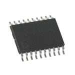
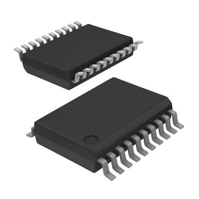
| 供应商器件封装 | 20-TSSOP |
| 关闭 | No |
| 其它名称 | 296-23881-2 |
| 功能 | Transceiver |
| 包装 | 带卷 (TR) |
| 协议 | RS232 |
| 单位重量 | 77 mg |
| 双工 | 全 |
| 商标 | Texas Instruments |
| 安装类型 | 表面贴装 |
| 安装风格 | SMD/SMT |
| 封装 | Reel |
| 封装/外壳 | 20-TSSOP(0.173",4.40mm 宽) |
| 封装/箱体 | TSSOP-20 |
| 工作温度 | -40°C ~ 125°C |
| 工作温度范围 | - 40 C to + 125 C |
| 工作电源电压 | 3.3 V, 5 V |
| 工厂包装数量 | 2000 |
| 接收器滞后 | 500mV |
| 接收机数量 | 2 Receiver |
| 数据速率 | 250kbps |
| 最大工作温度 | + 125 C |
| 最小工作温度 | - 40 C |
| 标准包装 | 2,000 |
| 激励器数量 | 2 Driver |
| 电压-电源 | 3 V ~ 5.5 V |
| 电源电流 | 1 mA |
| 类型 | 收发器 |
| 系列 | TRS3223-Q1 |
| 输入/输出端数量 | 8 |
| 驱动器/接收器数 | 2/2 |


- 商务部:美国ITC正式对集成电路等产品启动337调查
- 曝三星4nm工艺存在良率问题 高通将骁龙8 Gen1或转产台积电
- 太阳诱电将投资9.5亿元在常州建新厂生产MLCC 预计2023年完工
- 英特尔发布欧洲新工厂建设计划 深化IDM 2.0 战略
- 台积电先进制程称霸业界 有大客户加持明年业绩稳了
- 达到5530亿美元!SIA预计今年全球半导体销售额将创下新高
- 英特尔拟将自动驾驶子公司Mobileye上市 估值或超500亿美元
- 三星加码芯片和SET,合并消费电子和移动部门,撤换高东真等 CEO
- 三星电子宣布重大人事变动 还合并消费电子和移动部门
- 海关总署:前11个月进口集成电路产品价值2.52万亿元 增长14.8%


PDF Datasheet 数据手册内容提取
TRS3223-Q1 www.ti.com.......................................................................................................................................................................................... SLLS950–SEPTEMBER2008 3-V To 5.5-V MULTICHANNEL RS-232 LINE DRIVER/RECEIVER WITH ±15-kV ESD PROTECTION FEATURES 1 PWPACKAGE • QualifiedforAutomotiveApplications (TOPVIEW) • RS-232Bus-PinESDProtectionExceeds ±15kVUsingHuman-BodyModel(HBM) EN 1 20 FORCEOFF • MeetsorExceedstheRequirementsof C1+ 2 19 VCC V+ 3 18 GND TIA/EIA-232-FandITUv.28Standards C1- 4 17 DOUT1 • OperatesWith3-Vto5.5-VV Supply CC C2+ 5 16 RIN1 • Operatesupto250kbit/s C2- 6 15 ROUT1 • TwoDriversandTwoReceivers V- 7 14 FORCEON • LowStandbyCurrent...1m ATypical DOUT2 8 13 DIN1 • ExternalCapacitors...4×0.1m F RIN2 9 12 DIN2 • Accepts5-VLogicInputWith3.3-VSupply ROUT2 10 11 INVALID DESCRIPTION/ORDERING INFORMATION The TRS3223 consists of two line drivers, two line receivers, and a dual charge-pump circuit with ±15-kV ESD protection pin to pin (serial-port connection pins, including GND). The device meets the requirements of TIA/EIA-232-F and provides the electrical interface between an asynchronous communication controller and the serial-port connector. The charge pump and four small external capacitors allow operation from a single 3-V to 5.5-V supply. The device operates at data signaling rates up to 250 kbit/s and a maximum of 30-V/m s driver outputslewrate. Flexible control options for power management are available when the serial port is inactive. The auto-powerdown feature functions when FORCEON is low and FORCEOFF is high. During this mode of operation, if the device does not sense a valid RS-232 signal, the driver outputs are disabled. If FORCEOFF is set low and EN is high, both drivers and receivers are shut off, and the supply current is reduced to 1 m A. Disconnecting the serial port or turning off the peripheral drivers causes auto-powerdown to occur. Auto-powerdown can be disabled when FORCEON and FORCEOFF are high. With auto-powerdown enabled, the device is activated automatically when a valid signal is applied to any receiver input. The INVALID output is used to notify the user if an RS-232 signal is present at any receiver input. INVALID is high (valid data) if any receiver input voltage is greater than 2.7 V or less than –2.7 V, or has been between –0.3 V and 0.3 V for less than 30 m s. INVALID is low (invalid data) if the receiver input voltage is between –0.3 V and 0.3 V for more than 30m s.SeeFigure4forreceiverinputlevels. ORDERINGINFORMATION(1) T PACKAGE(2) ORDERABLEPARTNUMBER TOP-SIDEMARKING A –40°Cto125°C TSSOP–PW Reelof2000 TRS3223QPWRQ1 T3223 (1) Forthemostcurrentpackageandorderinginformation,seethePackageOptionAddendumattheendofthisdocument,orseetheTI websiteatwww.ti.com. (2) Packagedrawings,thermaldata,andsymbolizationareavailableatwww.ti.com/packaging. 1 Pleasebeawarethatanimportantnoticeconcerningavailability,standardwarranty,anduseincriticalapplicationsofTexas Instrumentssemiconductorproductsanddisclaimerstheretoappearsattheendofthisdatasheet. PRODUCTIONDATAinformationiscurrentasofpublicationdate. Copyright©2008,TexasInstrumentsIncorporated Products conform to specifications per the terms of the Texas Instruments standard warranty. Production processing does not necessarilyincludetestingofallparameters.
TRS3223-Q1 SLLS950–SEPTEMBER2008.......................................................................................................................................................................................... www.ti.com DRIVERFUNCTIONTABLE(EACHDRIVER)(1) INPUTS OUTPUT DIN FORCEON FORCEOFF VALIDRIN DOUT DRIVERSTATUS RS-232LEVEL X X L X Z Poweredoff L H H X H Normaloperationwithauto-powerdowndisabled H H H X L L L H Yes H Normaloperationwithauto-powerdownenabled H L H Yes L L L H No Z Poweredoffbyauto-powerdownfeature H L H No Z (1) H=highlevel,L=lowlevel,X=irrelevant,Z=highimpedance RECEIVERFUNCTIONTABLE(EACHRECEIVER)(1) INPUTS OUTPUT RIN EN VALIDRIN ROUT RS-232LEVEL L L X H H L X L X H X Z Open L No H (1) H=highlevel,L=lowlevel,X=irrelevant,Z=highimpedance(off), Open=inputdisconnectedorconnecteddriveroff LOGICDIAGRAM 13 17 DIN1 DOUT1 12 8 DIN2 DOUT2 20 FORCEOFF 11 14 Auto-powerdown INVALID FORCEON 1 EN 15 16 ROUT1 RIN1 10 9 ROUT2 RIN2 2 SubmitDocumentationFeedback Copyright©2008,TexasInstrumentsIncorporated ProductFolderLink(s):TRS3223-Q1
TRS3223-Q1 www.ti.com.......................................................................................................................................................................................... SLLS950–SEPTEMBER2008 ABSOLUTE MAXIMUM RATINGS(1)(2) overoperatingfree-airtemperaturerange(unlessotherwisenoted) V Supplyvoltagerange –0.3Vto6V CC V+ Positiveoutputsupplyvoltagerange –0.3Vto7V V– Negativeoutputsupplyvoltagerange 0.3Vto–7V V+–V– Supplyvoltagedifference 13V Driver,FORCEOFF,FORCEON,EN –0.3Vto6V V Inputvoltagerange I Receiver –25Vto25V Driver –13.2Vto13.2V V Outputvoltagerange O Receiver,INVALID –0.3VtoV +0.3V CC q Packagethermalimpedance(3) 83°C/W JA T Operatingvirtual-junctiontemperature 150°C J T Storagetemperaturerange –65°Cto150°C stg (1) Stressesbeyondthoselistedunderabsolutemaximumratingsmaycausepermanentdamagetothedevice.Thesearestressratings only,andfunctionaloperationofthedeviceattheseoranyotherconditionsbeyondthoseindicatedunderrecommendedoperating conditionsisnotimplied.Exposuretoabsolute-maximum-ratedconditionsforextendedperiodsmayaffectdevicereliability. (2) AllvoltagesarewithrespecttonetworkGND. (3) ThepackagethermalimpedanceiscalculatedinaccordancewithJESD51-7. RECOMMENDED OPERATING CONDITIONS(1) seeFigure6 MIN NOM MAX UNIT V =3.3V 3 3.3 3.6 CC V Supplyvoltage V CC V =5V 4.5 5 5.5 CC Driverandcontrol, VCC=3.3V 2 V High-levelinputvoltage V IH DIN,EN,FORCEOFF,FORCEON V =5V 2.4 CC V Low-levelinputvoltage Driverandcontrol,DIN,EN,FORCEOFF,FORCEON 0.8 V IL Driverandcontrol,DIN,EN,FORCEOFF,FORCEON 0 5.5 V Inputvoltage V I Receiver –25 25 T Operatingfree-airtemperature –40 125 °C A (1) TestconditionsareC1–C4=0.1m FatV =3.3V±0.3V;C1=0.047m F,C2–C4=0.33m FatV =5V±0.5V. CC CC ELECTRICAL CHARACTERISTICS(1) overrecommendedrangesofsupplyvoltageandoperatingfree-airtemperature(unlessotherwisenoted)(seeFigure6) PARAMETER TESTCONDITIONS MIN TYP(2) MAX UNIT I Inputleakagecurrent EN,FORCEOFF,FORCEON ±0.01 ±1 m A I Auto-powerdown Noload,FORCEOFFand 0.3 2 mA disabled FORCEONatV CC Poweredoff V =3.3Vor5V, Noload,FORCEOFFatGND 1 20 I Supplycurrent CC CC T =25°C Auto-powerdown A Noload,FORCEOFFatVCC, m A FORCEONatGND, 1 20 enabled AllRINareopenorgrounded (1) TestconditionsareC1–C4=0.1m FatV =3.3V±0.3V;C1=0.047m F,C2–C4=0.33m FatV =5V±0.5V. CC CC (2) AlltypicalvaluesareatV =3.3VorV =5V,andT =25°C. CC CC A Copyright©2008,TexasInstrumentsIncorporated SubmitDocumentationFeedback 3 ProductFolderLink(s):TRS3223-Q1
TRS3223-Q1 SLLS950–SEPTEMBER2008.......................................................................................................................................................................................... www.ti.com DRIVER SECTION ELECTRICAL CHARACTERISTICS(1) overrecommendedrangesofsupplyvoltageandoperatingfree-airtemperature(unlessotherwisenoted)(seeFigure6) PARAMETER TESTCONDITIONS MIN TYP(2) MAX UNIT V High-leveloutputvoltage DOUTatR =3kΩtoGND 5 5.4 V OH L V Low-leveloutputvoltage DOUTatR =3kΩtoGND –5 –5.4 V OL L I High-levelinputcurrent V =V ±0.01 ±1 m A IH I CC I Low-levelinputcurrent V =GND ±0.01 ±1 m A IL I V =3.6V,V =0V ±35 ±60 I Short-circuitoutputcurrent(3) CC O mA OS V =5.5V,V =0V ±35 ±60 CC O r Outputresistance V ,V+,andV–=0V,V =±2V 300 10M Ω o CC O V =±12V,V =3Vto3.6V ±25 I Outputleakagecurrent FORCEOFF=GND O CC m A off V =±10V,V =4.5Vto5.5V ±25 O CC (1) TestconditionsareC1–C4=0.1m FatV =3.3V±0.3V;C1=0.047m F,C2–C4=0.33m FatV =5V±0.5V. CC CC (2) AlltypicalvaluesareatV =3.3VorV =5V,andT =25°C. CC CC A (3) Short-circuitdurationsshouldbecontrolledtopreventexceedingthedeviceabsolutepower-dissipationratings,andnotmorethanone outputshouldbeshortedatatime. DRIVER SECTION SWITCHING CHARACTERISTICS(1) overrecommendedrangesofsupplyvoltageandoperatingfree-airtemperature(unlessotherwisenoted)(seeFigure6) PARAMETER TESTCONDITIONS MIN TYP(2) MAX UNIT Maximumdatarate C =1000pF,OneDOUTswitching,R =3kΩ(seeFigure1) 250 kbit/s L L t Pulseskew(3) C =150pFto2500pF,R =3kΩto7kΩ(seeFigure2) 100 ns sk(p) L L SR(tr) Slewrate,transitionregion V =3.3V,R =3kΩto7kΩ CL=150pFto1000pF 6 30 V/m s (seeFigure1) CC L C =150pFto2500pF 4 30 L (1) TestconditionsareC1–C4=0.1m FatV =3.3V±0.3V;C1=0.047m F,C2–C4=0.33m FatV =5V±0.5V. CC CC (2) AlltypicalvaluesareatV =3.3VorV =5V,andT =25°C. CC CC A (3) Pulseskewisdefinedas|t –t |ofeachchannelofthesamedevice. PLH PHL 4 SubmitDocumentationFeedback Copyright©2008,TexasInstrumentsIncorporated ProductFolderLink(s):TRS3223-Q1
TRS3223-Q1 www.ti.com.......................................................................................................................................................................................... SLLS950–SEPTEMBER2008 RECEIVER SECTION ELECTRICAL CHARACTERISTICS(1) overrecommendedrangesofsupplyvoltageandoperatingfree-airtemperature(unlessotherwisenoted)(seeFigure6) PARAMETER TESTCONDITIONS MIN TYP(2) MAX UNIT V High-leveloutputvoltage I =–1mA V –0.6 V –0.1 V OH OH CC CC V Low-leveloutputvoltage I =1.6mA 0.4 V OL OL V =3.3V 1.6 2.4 CC V Positive-goinginputthresholdvoltage V IT+ V =5V 1.9 2.4 CC V =3.3V 0.6 1.1 CC V Negative-goinginputthresholdvoltage V IT– V =5V 0.8 1.4 CC V Inputhysteresis(V –V ) 0.5 V hys IT+ IT– I Outputleakagecurrent EN=V ±0.05 ±10 m A off CC r Inputresistance V =±3Vto±25V 3 5 8.3 kΩ i I (1) TestconditionsareC1–C4=0.1m FatV =3.3V±0.3V;C1=0.047m F,C2–C4=0.33m FatV =5V±0.5V. CC CC (2) AlltypicalvaluesareatV =3.3VorV =5V,andT =25°C. CC CC A RECEIVER SECTION SWITCHING CHARACTERISTICS(1) overrecommendedrangesofsupplyvoltageandoperatingfree-airtemperature(unlessotherwisenoted)(seeFigure6) PARAMETER TESTCONDITIONS TYP(2) UNIT t Propagationdelaytime,low-leveltohigh-leveloutput C =150pF,SeeFigure3 150 ns PLH L t Propagationdelaytime,high-leveltolow-leveloutput C =150pF,SeeFigure3 150 ns PHL L t Outputenabletime C =150pF,R =3kΩ,SeeFigure4 200 ns en L L t Outputdisabletime C =150pF,R =3kΩ,SeeFigure4 200 ns dis L L t Pulseskew(3) SeeFigure3 50 ns sk(p) (1) TestconditionsareC1–C4=0.1m FatV =3.3V±0.3V;C1=0.047m F,C2–C4=0.33m FatV =5V±0.5V. CC CC (2) AlltypicalvaluesareatV =3.3VorV =5V,andT =25°C. CC CC A (3) Pulseskewisdefinedas|t –t |ofeachchannelofthesamedevice. PLH PHL Copyright©2008,TexasInstrumentsIncorporated SubmitDocumentationFeedback 5 ProductFolderLink(s):TRS3223-Q1
TRS3223-Q1 SLLS950–SEPTEMBER2008.......................................................................................................................................................................................... www.ti.com AUTO-POWERDOWN SECTION ELECTRICAL CHARACTERISTICS overrecommendedrangesofsupplyvoltageandoperatingfree-airtemperature(unlessotherwisenoted)(seeFigure5) PARAMETER TESTCONDITIONS MIN MAX UNIT ReceiverinputthresholdforINVALID V FORCEON=GND,FORCEOFF=V 2.7 V T+(valid) high-leveloutputvoltage CC ReceiverinputthresholdforINVALID V FORCEON=GND,FORCEOFF=V –2.7 V T–(valid) high-leveloutputvoltage CC ReceiverinputthresholdforINVALID V FORCEON=GND,FORCEOFF=V –0.3 0.3 V T(invalid) low-leveloutputvoltage CC V INVALIDhigh-leveloutputvoltage I =–1mA,FORCEON=GND,FORCEOFF=V V –0.6 V OH OH CC CC V INVALIDlow-leveloutputvoltage I =1.6mA,FORCEON=GND,FORCEOFF=V 0.4 V OL OL CC AUTO-POWERDOWN SECTION SWITCHING CHARACTERISTICS overrecommendedrangesofsupplyvoltageandoperatingfree-airtemperature(unlessotherwisenoted)(seeFigure5) PARAMETER TYP(1) UNIT t Propagationdelaytime,low-tohigh-leveloutput 1 m s valid t Propagationdelaytime,high-tolow-leveloutput 30 m s invalid t Supplyenabletime 100 m s en (1) AlltypicalvaluesareatV =3.3VorV =5V,andT =25°C. CC CC A 6 SubmitDocumentationFeedback Copyright©2008,TexasInstrumentsIncorporated ProductFolderLink(s):TRS3223-Q1
TRS3223-Q1 www.ti.com.......................................................................................................................................................................................... SLLS950–SEPTEMBER2008 PARAMETER MEASUREMENT INFORMATION 3V Input 1.5V 1.5V RS-232 0V Output Generator (see Note B) 50Ω CL tTHL tTLH RL (see Note A) 3V 3V 3V VOH Output FORCEOFF -3 V -3 V VOL TEST CIRCUIT VOLTAGEWAVEFORMS 6V SR(tr) t ort THL TLH A.CLincludes probe and jig capacitance. B.The pulse generator has the following characteristics:PRR = 250 kbit/s, ZO= 50Ω, 50% duty cycle, tr≤10 ns, tf≤10 ns. Figure1.DriverSlewRate 3V Input 1.5V 1.5V RS-232 0V Output Generator 50Ω (see Note B) CL tPHL tPLH RL (see Note A) VOH 3V Output 50% 50% FORCEOFF VOL TEST CIRCUIT VOLTAGEWAVEFORMS A.CLincludes probe and jig capacitance. B.The pulse generator has the following characteristics:PRR = 250 kbit/s, ZO= 50Ω, 50% duty cycle, tr≤10 ns, tf≤10 ns. Figure2.DriverPulseSkew EN 3V 0V Input 1.5V 1.5V -3 V Output Generator 50Ω (see Note B) CL tPHL tPLH (see Note A) VOH 0V Output 50% 50% FORCEOFF VOL TEST CIRCUIT VOLTAGEWAVEFORMS A.CLincludes probe and jig capacitance. B.The pulse generator has the following characteristics:ZO= 50Ω, 50% duty cycle, tr≤10 ns, tf≤10 ns. Figure3.ReceiverPropagationDelayTimes Copyright©2008,TexasInstrumentsIncorporated SubmitDocumentationFeedback 7 ProductFolderLink(s):TRS3223-Q1
TRS3223-Q1 SLLS950–SEPTEMBER2008.......................................................................................................................................................................................... www.ti.com PARAMETER MEASUREMENT INFORMATION (continued) 3V VCC GND Input 1.5V 1.5V FORCEON S1 0V 3V or 0V tPHZ tPHZ RL (S1 at GND) (S1 at GND) 3V or 0V Output VOH Output 50% CL EN (see Note A) 0.3V tPLZ (S1 atVCC) Generator 0.3V 50Ω (see Note B) Output 50% VOL tPZL (S1 atVCC) TEST CIRCUIT VOLTAGEWAVEFORMS A.CLincludes probe and jig capacitance. B.The pulse generator has the following characteristics:ZO= 50Ω, 50% duty cycle, tr≤10 ns, tf≤10 ns. Figure4.ReceiverEnableandDisableTimes 8 SubmitDocumentationFeedback Copyright©2008,TexasInstrumentsIncorporated ProductFolderLink(s):TRS3223-Q1
TRS3223-Q1 www.ti.com.......................................................................................................................................................................................... SLLS950–SEPTEMBER2008 PARAMETER MEASUREMENT INFORMATION (continued) 3V 2.7V 2.7V Receiver 0V Input 0V ROUT -2.7 V -2.7 V -3 V Generator 50Ω (see Note B) tinvalid tvalid VCC INVALID 50%VCC 50%VCC Output 0V Auto- INVALID ten powerdown CL= 30 pF V+ ≈V+ (see Note A) 0.3V Supply VCC FORCEOFF Voltages 0V 0.3V DIN DOUT FORCEON V- ≈V- TEST CIRCUIT VOLTAGEWAVEFORMS Valid RS-232 level,INVALIDhigh 2.7V Indeterminate 0.3V If signal remains within this region 0V for more than 30 µs,INVALIDis low† -0.3 V Indeterminate -2.7 V Valid RS-232 level,INVALIDhigh †Auto-powerdowndisables drivers and reducessupply current to 1 µA. A.CLincludes probe and jig capacitance. B.The pulse generator has the following characteristics:PRR = 5 kbit/s, ZO= 50Ω, 50% duty cycle, tr≤10 ns, tf≤10 ns. Figure5.INVALIDPropagationDelayTimesandSupplyEnablingTime Copyright©2008,TexasInstrumentsIncorporated SubmitDocumentationFeedback 9 ProductFolderLink(s):TRS3223-Q1
TRS3223-Q1 SLLS950–SEPTEMBER2008.......................................................................................................................................................................................... www.ti.com APPLICATION INFORMATION 1 Auto 20 EN FORCEOFF Powerdown 2 19 C1+ VCC + CBYPASS - (0.1 µF) + 3 18 C1 + V+ GND - C3 - 4 17 C1- DOUT1 5 16 C2+ RIN1 + C2 - 6 15 C2- ROUT1 5 kΩ 7 14 V- FORCEON - C4 + 8 13 DOUT2 DIN1 9 12 RIN2 DIN2 10 11 ROUT2 INVALID 5kΩ A.C3 can be connected toVCCor GND. B.Resistor values shown are nominal. C.Nonpolarized ceramic capacitors are acceptable.If polarized tantalum or electrolytic capacitors are used, they should be connected as shown. VCCvs CAPACITORVALUES VCC C1 C2,C3,C4 3.3V±0.3V 0.1 µF 0.1µF 5V±0.5V 0.047µF 0.33µF 3V to 5.5V 0.1µF 0.47µF Figure6.TypicalOperatingCircuitandCapacitorValues 10 SubmitDocumentationFeedback Copyright©2008,TexasInstrumentsIncorporated ProductFolderLink(s):TRS3223-Q1
PACKAGE MATERIALS INFORMATION www.ti.com 2-Oct-2019 TAPE AND REEL INFORMATION *Alldimensionsarenominal Device Package Package Pins SPQ Reel Reel A0 B0 K0 P1 W Pin1 Type Drawing Diameter Width (mm) (mm) (mm) (mm) (mm) Quadrant (mm) W1(mm) TRS3223QPWRQ1 TSSOP PW 20 2000 330.0 16.4 6.95 7.0 1.4 8.0 16.0 Q1 PackMaterials-Page1
PACKAGE MATERIALS INFORMATION www.ti.com 2-Oct-2019 *Alldimensionsarenominal Device PackageType PackageDrawing Pins SPQ Length(mm) Width(mm) Height(mm) TRS3223QPWRQ1 TSSOP PW 20 2000 367.0 367.0 38.0 PackMaterials-Page2
None
None
IMPORTANTNOTICEANDDISCLAIMER TIPROVIDESTECHNICALANDRELIABILITYDATA(INCLUDINGDATASHEETS),DESIGNRESOURCES(INCLUDINGREFERENCE DESIGNS),APPLICATIONOROTHERDESIGNADVICE,WEBTOOLS,SAFETYINFORMATION,ANDOTHERRESOURCES“ASIS” ANDWITHALLFAULTS,ANDDISCLAIMSALLWARRANTIES,EXPRESSANDIMPLIED,INCLUDINGWITHOUTLIMITATIONANY IMPLIEDWARRANTIESOFMERCHANTABILITY,FITNESSFORAPARTICULARPURPOSEORNON-INFRINGEMENTOFTHIRD PARTYINTELLECTUALPROPERTYRIGHTS. TheseresourcesareintendedforskilleddevelopersdesigningwithTIproducts.Youaresolelyresponsiblefor(1)selectingtheappropriate TIproductsforyourapplication,(2)designing,validatingandtestingyourapplication,and(3)ensuringyourapplicationmeetsapplicable standards,andanyothersafety,security,orotherrequirements.Theseresourcesaresubjecttochangewithoutnotice.TIgrantsyou permissiontousetheseresourcesonlyfordevelopmentofanapplicationthatusestheTIproductsdescribedintheresource.Other reproductionanddisplayoftheseresourcesisprohibited.NolicenseisgrantedtoanyotherTIintellectualpropertyrightortoanythird partyintellectualpropertyright.TIdisclaimsresponsibilityfor,andyouwillfullyindemnifyTIanditsrepresentativesagainst,anyclaims, damages,costs,losses,andliabilitiesarisingoutofyouruseoftheseresources. TI’sproductsareprovidedsubjecttoTI’sTermsofSale(www.ti.com/legal/termsofsale.html)orotherapplicabletermsavailableeitheron ti.comorprovidedinconjunctionwithsuchTIproducts.TI’sprovisionoftheseresourcesdoesnotexpandorotherwisealterTI’sapplicable warrantiesorwarrantydisclaimersforTIproducts. MailingAddress:TexasInstruments,PostOfficeBox655303,Dallas,Texas75265 Copyright©2019,TexasInstrumentsIncorporated