ICGOO在线商城 > 集成电路(IC) > 接口 - 驱动器,接收器,收发器 > FIN1019MTCX

 Datasheet下载
- 型号: FIN1019MTCX
- 制造商: Fairchild Semiconductor
- 库位|库存: xxxx|xxxx
- 要求:
| 数量阶梯 | 香港交货 | 国内含税 |
| +xxxx | $xxxx | ¥xxxx |
查看当月历史价格
查看今年历史价格
FIN1019MTCX产品简介:
ICGOO电子元器件商城为您提供FIN1019MTCX由Fairchild Semiconductor设计生产,在icgoo商城现货销售,并且可以通过原厂、代理商等渠道进行代购。 FIN1019MTCX价格参考¥5.91-¥5.91。Fairchild SemiconductorFIN1019MTCX封装/规格:接口 - 驱动器,接收器,收发器, 1/1 Transceiver Full LVDS 14-TSSOP。您可以下载FIN1019MTCX参考资料、Datasheet数据手册功能说明书,资料中有FIN1019MTCX 详细功能的应用电路图电压和使用方法及教程。
ON Semiconductor(安森美)的FIN1019MTCX是一款高速差分数据传输接口芯片,属于接口类中的驱动器/接收器/收发器产品。该器件采用8引脚TSSOP封装,主要功能是将单端信号转换为低电压差分信号(LVDS),或反之,实现高速、低功耗、低噪声的数据传输。

FIN1019MTCX广泛应用于需要高带宽和抗干扰能力的场景。典型应用包括:工业自动化控制系统中的远程数据通信模块;高性能成像设备,如医疗影像系统、工业摄像头等,用于高速图像数据的可靠传输;通信基础设施中的背板接口、基站模块间连接;以及消费类高端显示设备,如大尺寸液晶面板、视频处理单元之间的信号传输。

其低功耗特性使其适用于对能效要求较高的便携式或嵌入式系统。此外,由于具备良好的电磁兼容性(EMC)和抗噪声能力,FIN1019MTCX也适合在复杂电磁环境中稳定运行,例如工厂自动化、车载信息娱乐系统及安防监控系统。

综上所述,FIN1019MTCX凭借其高速率、低延迟和高可靠性,成为多种电子系统中实现点对点串行通信的理想选择,尤其适用于对信号完整性要求较高的中短距离数据传输场合。
| 参数 | 数值 |
| 产品目录 | 集成电路 (IC)半导体 |
| 描述 | IC DRVR/RCVR3.3V LVDS HS 14TSSOP缓冲器和线路驱动器 3.3V Driver/Receiver Hi Speed Diff LVDS |
| 产品分类 | |
| 品牌 | Fairchild Semiconductor |
| 产品手册 | |
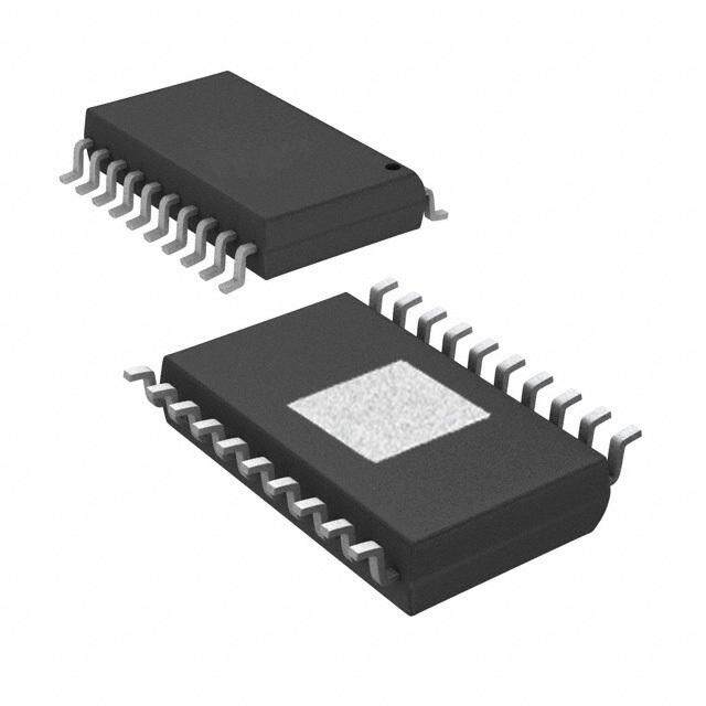
| 产品图片 |
|
| rohs | 符合RoHS无铅 / 符合限制有害物质指令(RoHS)规范要求 |
| 产品系列 | 逻辑集成电路,缓冲器和线路驱动器,Fairchild Semiconductor FIN1019MTCX- |
| 数据手册 | |
| 产品型号 | FIN1019MTCX |
| 产品种类 | 缓冲器和线路驱动器 |
| 传播延迟时间 | 2.5 ns |
| 供应商器件封装 | 14-TSSOP |
| 其它名称 | FIN1019MTCXDKR |
| 包装 | Digi-Reel® |
| 协议 | LVDS |
| 单位重量 | 55.300 mg |
| 双工 | 全 |
| 商标 | Fairchild Semiconductor |
| 安装类型 | 表面贴装 |
| 安装风格 | SMD/SMT |
| 封装 | Reel |
| 封装/外壳 | 14-TSSOP(0.173",4.40mm 宽) |
| 封装/箱体 | TSSOP-14 |
| 工作温度 | -40°C ~ 85°C |
| 工厂包装数量 | 2500 |
| 接收器滞后 | - |
| 数据速率 | 400Mbps |
| 最大工作温度 | + 85 C |
| 最小工作温度 | - 40 C |
| 标准包装 | 1 |
| 电压-电源 | 3 V ~ 3.6 V |
| 电源电压-最大 | 3.6 V |
| 电源电压-最小 | 3 V |
| 电源电流 | 12.5 mA |
| 类型 | 收发器 |
| 系列 | FIN1019 |
| 输入线路数量 | 1 |
| 输出线路数量 | 1 |
| 逻辑类型 | High Speed Differential Driver and Receiver |
| 逻辑系列 | FIN10 |
| 零件号别名 | FIN1019MTCX_NL |
| 驱动器/接收器数 | 1/1 |


- 商务部:美国ITC正式对集成电路等产品启动337调查
- 曝三星4nm工艺存在良率问题 高通将骁龙8 Gen1或转产台积电
- 太阳诱电将投资9.5亿元在常州建新厂生产MLCC 预计2023年完工
- 英特尔发布欧洲新工厂建设计划 深化IDM 2.0 战略
- 台积电先进制程称霸业界 有大客户加持明年业绩稳了
- 达到5530亿美元!SIA预计今年全球半导体销售额将创下新高
- 英特尔拟将自动驾驶子公司Mobileye上市 估值或超500亿美元
- 三星加码芯片和SET,合并消费电子和移动部门,撤换高东真等 CEO
- 三星电子宣布重大人事变动 还合并消费电子和移动部门
- 海关总署:前11个月进口集成电路产品价值2.52万亿元 增长14.8%


PDF Datasheet 数据手册内容提取
Is Now Part of To learn more about ON Semiconductor, please visit our website at www.onsemi.com Please note: As part of the Fairchild Semiconductor integration, some of the Fairchild orderable part numbers will need to change in order to meet ON Semiconductor’s system requirements. Since the ON Semiconductor product management systems do not have the ability to manage part nomenclature that utilizes an underscore (_), the underscore (_) in the Fairchild part numbers will be changed to a dash (-). This document may contain device numbers with an underscore (_). Please check the ON Semiconductor website to verify the updated device numbers. The most current and up-to-date ordering information can be found at www.onsemi.com. Please email any questions regarding the system integration to Fairchild_questions@onsemi.com. ON Semiconductor and the ON Semiconductor logo are trademarks of Semiconductor Components Industries, LLC dba ON Semiconductor or its subsidiaries in the United States and/or other countries. ON Semiconductor owns the rights to a number of patents, trademarks, copyrights, trade secrets, and other intellectual property. A listing of ON Semiconductor’s product/patent coverage may be accessed at www.onsemi.com/site/pdf/Patent-Marking.pdf. ON Semiconductor reserves the right to make changes without further notice to any products herein. ON Semiconductor makes no warranty, representation or guarantee regarding the suitability of its products for any particular purpose, nor does ON Semiconductor assume any liability arising out of the application or use of any product or circuit, and specifically disclaims any and all liability, including without limitation special, consequential or incidental damages. Buyer is responsible for its products and applications using ON Semiconductor products, including compliance with all laws, regulations and safety requirements or standards, regardless of any support or applications information provided by ON Semiconductor. “Typical” parameters which may be provided in ON Semiconductor data sheets and/or specifications can and do vary in different applications and actual performance may vary over time. All operating parameters, including “Typicals” must be validated for each customer application by customer’s technical experts. ON Semiconductor does not convey any license under its patent rights nor the rights of others. ON Semiconductor products are not designed, intended, or authorized for use as a critical component in life support systems or any FDA Class 3 medical devices or medical devices with a same or similar classification in a foreign jurisdiction or any devices intended for implantation in the human body. Should Buyer purchase or use ON Semiconductor products for any such unintended or unauthorized application, Buyer shall indemnify and hold ON Semiconductor and its officers, employees, subsidiaries, affiliates, and distributors harmless against all claims, costs, damages, and expenses, and reasonable attorney fees arising out of, directly or indirectly, any claim of personal injury or death associated with such unintended or unauthorized use, even if such claim alleges that ON Semiconductor was negligent regarding the design or manufacture of the part. ON Semiconductor is an Equal Opportunity/Affirmative Action Employer. This literature is subject to all applicable copyright laws and is not for resale in any manner.
F April 2001 IN Revised September 2001 1 0 1 9 3 FIN1019 .3 V 3.3V LVDS High Speed Differential Driver/Receiver L V D General Description Features S H This driver and receiver pair are designed for high speed (cid:1) Greater than 400Mbs data rate ig interconnects utilizing Low Voltage Differential Signaling (cid:1) 3.3V power supply operation h (LVDS) technology. The driver translates LVTTL signals to (cid:1) 0.5ns maximum differential pulse skew S L3V50DmSV l eavnedls thwei thre cae ivtyepr ictraal nsdliaffteerse nLtViaDl So ustipgunta lssw, winigth oaf (cid:1) 2.5ns maximum propagation delay pe typical differential input threshold of 100mV, into LVTTL (cid:1) Low power dissipation e d levels. LVDS technology provides low EMI at ultra low (cid:1) Power-Off protection D pidoewael rfo dr ihssigipha stipoene edv celonc akt ohri gdha tfare tqraunesnfecire.s. This device is (cid:1)(cid:1) 1F0a0il msaVf ere pcreoitveecrt iionnp uotp seenn-sciitricvuitiyt, shorted and terminated iffe conditions re (cid:1) Meets or exceeds the TIA/EIA-644 LVDS standard n t (cid:1) Flow-through pinout simplifies PCB layout ia (cid:1) 14-Lead SOIC and TSSOP packages save space l D r i v Ordering Code: e r / R Order Number Package Number Package Description e c FIN1019M M14A 14-Lead Small Outline Integrated Circuit (SOIC), JEDEC MS-012, 0.150" Narrow e i FIN1019MTC MTC14 14-Lead Thin Shrink Small Outline Package (TSSOP), JEDEC MO-153, 4.4mm Wide v e Devices also available in Tape and Reel. Specify by appending the suffix letter “X” to the ordering code. r Function Table Connection Diagram Inputs Outputs RIN+ RIN− RE ROUT L H L L H L L H X X H Z Fail Safe Condition L H DIN DE DOUT+ DOUT− L H L H Pin Descriptions H H H L X L Z Z Pin Name Description Open−Circuit or Z H L H DIN LVTTL Data Input HZ == HHiIgGhH I mLopgeidca Lnecveel FLa =il LSOafWe =L oOgpice nL,e Svehlorted, TeXrm =i nDaotend’t Care DOUT+ Non-inverting LVDS Output DOUT− Inverting LVDS Output DE Driver Enable (LVTTL, Active HIGH) RIN+ Non-Inverting LVDS Input RIN− Inverting LVDS Input ROUT LVTTL Receiver Output RE Receiver Enable (LVTTL, Active LOW) VCC Power Supply GND Ground NC No Connect © 2001 Fairchild Semiconductor Corporation DS500506 www.fairchildsemi.com
9 1 Absolute Maximum Ratings Recommended Operating 0 (Note 1) 1 Conditions N Supply Voltage (VCC) −0.5V to +4.6V FI LVTTL DC Input Voltage (DIN, DE, RE) −0.5V to +6V Supply Voltage (VCC) 3.0V to 3.6V LVDS DC Input Voltage (RIN+, RIN−) −0.5V to 4.7V Input Voltage (VIN) 0 to VCC LVTTL DC Output Voltage (ROUT) −0.5V to +6V Magnitude of Differential Voltage LVDS DC Output Voltage (DOUT+, DOUT−) −0.5V to 4.7V (|VID|) 100 mV to VCC LVDS Driver Short Circuit Current (IOSD) Continuous Common-Mode Input Voltage (VIC) 0.05V to 2.35V LVTTL DC Output Current (IO) 16 mA Operating Temperature (TA) −40°C to +85°C Storage Temperature Range (TSTG) −65°C to +150°C Max Junction Temperature (TJ) 150°C Lead Temperature (TL) Note 1: The “Absolute Maximum Ratings”: are those values beyond which (Soldering, 10 seconds) 260°C damage to the device may occur. The databook specifications should be met, without exception, to ensure that the system design is reliable over its ESD (Human Body Model) ≥ 6500V power supply, temperature and output/input loading variables. Fairchild ESD (Machine Model) ≥ 300V does not recommend operation of circuits outside databook specification. DC Electrical Characteristics Over supply voltage and operating temperature ranges, unless otherwise specified Min Typ Max Symbol Parameter Test Conditions Units (Note 2) LVDS Differential Driver Characteristics VOD Output Differential Voltage 250 350 450 mV ∆VOD VOD Magnitude Change from 25 mV Differential LOW-to-HIGH RL = 100Ω, See Figure 1 VOS Offset Voltage 1.125 1.25 1.375 V ∆VOS Offset Magnitude Change from 25 mV Differential LOW-to-HIGH IOZD Disabled Output Leakage Current VOUT = VCC or GND, DE = 0V ±20 µA IOFF Power Off Output Current VCC = 0V, VOUT = 0V or 3.6V ±20 µA IOS Short Circuit Output Current VOUT = 0V, DE = VCC −8 mA VOD = 0V, DE = VCC ±8 LVTTL Driver Characteristics VOH Output HIGH Voltage SIOeHe = F −ig1u0r0e µ6A a,n RdE T a=b 0leV ,1 VCC −0.2 V IOH = −8 mA, RE = 0V, VID = 400 mV 2.4 VID = 400 mV, VIC = 1.2V, see Figure 6 VOL Output LOW Voltage IOL = 100 µA, RE = 0V, VID = −400 mV 0.2 See Figure 6 and Table 1 V IOL = −8 mA, RE = 0V, VID = −400 mV 0.5 VID = −400 mV, VIC = 1.2V, see Figure 6 IOZ Disabled Output Leakage Current VOUT = VCC or GND, RE = VCC ±20 µA LVDS Receiver Characteristics VTH Differential Input Threshold HIGH See Figure 6 and Table 1 100 mV VTL Differential Input Threshold LOW See Figure 6 and Table 1 −100 mV IIN Input Current VIN = 0V or VCC ±20 µA II(OFF) Power-OFF Input Current VCC = 0V, VIN = 0V or 3.6V ±20 µA LVTTL Driver and Control Signals Characteristics VIH Input HIGH Voltage 2.0 VCC V VIL Input LOW Voltage GND 0.8 V IIN Input Current VIN = 0V or VCC ±20 µA II(OFF) Power-OFF Input Current VCC = 0V, VIN = 0V or 3.6V ±20 µA VIK Input Clamp Voltage IIK = −18 mA −1.5 V www.fairchildsemi.com 2
F DC Electrical Characteristics (Continued) IN 1 Device Characteristics 0 ICC Power Supply Current Driver Enabled, Driver Load: RL = 100 Ω 12.5 mA 19 Receiver Disabled, No Receiver Load Driver Enabled, Driver Load: RL = 100 Ω, Receiver Enabled, (RIN+ = 1V and RIN− = 1.4V) 12.5 mA or (RIN+ = 1.4V and ROUT− = 1V) Driver Disabled, Receiver Enabled, (RIN+ = 1V and RIN− = 1.4V) or 7.0 mA (RIN+ = 1.4V and RIN− = 1V) Driver Disabled, Receiver Disabled 7.0 mA CIN Input Capacitance Any LVTTL or LVDS Input 4 pF COUT Output Capacitance Any LVTTL or LVDS Output 6 pF Note 2: All typical values are at TA = 25°C and with VCC = 3.3V. AC Electrical Characteristics Over supply voltage and operating temperature ranges, unless otherwise specified Min Typ Max Symbol Parameter Test Conditions Units (Note 3) Driver Timing Characteristics tPLHD Differential Propagation Delay 0.5 1.5 ns LOW-to-HIGH tPHLD Differential Propagation Delay 0.5 1.5 ns HIGH-to-LOW RL = 100 Ω, CL = 10 pF, tTLHD Differential Output Rise Time (20% to 80%) See Figure 2 and Figure 3 0.4 1.0 ns tTHLD Differential Output Fall Time (80% to 20%) 0.4 1.0 ns tSK(P) Pulse Skew |tPLH - tPHL| 0.5 ns tSK(PP) Part-to-Part Skew (Note 4) 1.0 ns tZHD Differential Output Enable Time from Z to HIGH RL = 100Ω, CL = 10 pF, 5.0 ns tZLD Differential Output Enable Time from Z to LOW See Figure 4 and Figure 5 5.0 ns tHZD Differential Output Disable Time from HIGH to Z 5.0 ns tLZD Differential Output Disable Time from LOW to Z 5.0 ns Receiver Timing Characteristics tPLH Propagation Delay LOW-to-HIGH 0.9 2.5 ns tPHL Propagation Delay HIGH-to-LOW 0.9 2.5 ns tTLH Output Rise time (20% to 80%) |VID| = 400 mV, CL = 10 pF, 0.5 ns tTHL Output Fall time (80% to 20%) See Figure 6 and Figure 7 0.5 ns tSK(P) Pulse Skew | tPLH - tPHL | 0.5 ns tSK(PP) Part-to-Part Skew (Note 4) 1.0 ns tZH LVTTL Output Enable Time from Z to HIGH 5.0 ns tZL LVTTL Output Enable Time from Z to LOW RL = 500 Ω, CL = 10 pF, 5.0 ns tHZ LVTTL Output Disable Time from HIGH to Z See Figure 8 5.0 ns tLZ LVTTL Output Disable Time from LOW to Z 5.0 ns Note 3: All typical values are at TA = 25°C and with VCC = 5V. Note 4: tSK(PP) is the magnitude of the difference in propagation delay times between any specified terminals of two devices switching in the same direction (either LOW-to-HIGH or HIGH-to-LOW) when both devices operate with the same supply voltage, same temperature, and have identical test circuits. 3 www.fairchildsemi.com
9 1 0 1 N I F Note A: Input pulses have frequency = 10 MHz, tR or tF = 2 ns Note B: CL includes all probe and fixture capacitances FIGURE 1. Differential Driver DC Test Circuit FIGURE 2. Differential Driver Propagation Delay and Transition Time Test Circuit Note B: Input pulses have the frequency = 10 MHz, tR or tF = 2 ns Note A: CL includes all probe and fixture capacitances FIGURE 4. Differential Driver Enable and FIGURE 3. AC Waveforms for Differential Driver Disable Test Circuit FIGURE 5. Enable and Disable AC Waveforms www.fairchildsemi.com 4
F IN 1 0 1 9 Note A: Input pulses have frequency = 10 MHz, tR or tF = 1ns Note B: CL includes all probe and fixture capacitance FIGURE 6. Differential Receiver Voltage Definitions and Propagation Delay and Transition Time Test Circuit TABLE 1. Receiver Minimum and Maximum Input Threshold Test Voltages Applied Voltages (V) Resulting Differential Resulting Common Mode Input Voltage (mV) Input Voltage (V) VIA VIB VID VIC 1.25 1.15 100 1.2 1.15 1.25 −100 1.2 2.4 2.3 100 2.35 2.3 2.4 −100 2.35 0.1 0 100 0.05 0 0.1 −100 0.05 1.5 0.9 600 1.2 0.9 1.5 −600 1.2 2.4 1.8 600 2.1 1.8 2.4 −600 2.1 0.6 0 600 0.3 0 0.6 −600 0.3 5 www.fairchildsemi.com
9 1 0 1 N I F FIGURE 7. LVDS Input to LVTTL Output AC Waveforms Test Circuit for LVTTL Outputs Voltage Waveforms Enable and Disable Times FIGURE 8. LVTTL Outputs Test Circuit and AC Waveforms www.fairchildsemi.com 6
F DC / AC Typical Performance Curves IN 1 Drivers 0 1 9 FIGURE 10. Output Low Voltage vs. FIGURE 9. Output High Voltage vs. Power Supply Voltage Power Supply Voltage FIGURE 11. Output Short Circuit Current vs. FIGURE 12. Differential Output Voltage vs. Power Supply Voltage Power Supply Voltage FIGURE 13. Differential Output Voltage vs. FIGURE 14. Offset Voltage vs. Load Resistor Power Supply Voltage 7 www.fairchildsemi.com
9 1 DC / AC Typical Performance Curves 0 (Continued) 1 N I F FIGURE 15. Power Supply Current vs. FIGURE 16. Power Supply Current vs. Frequency Power Supply Voltage FIGURE 17. Power Supply Current vs. FIGURE 18. Differential Propagation Delay vs. Ambient Temperature Power Supply FIGURE 19. Differential Propagation Delay vs. FIGURE 20. Differential Skew (tPLH - tPHL) vs. Ambient Temperature Power Supply Voltage www.fairchildsemi.com 8
F DC / AC Typical Performance Curves (Continued) IN 1 0 1 9 FIGURE 21. Differential Pulse Skew (tPLH - tPHL) vs. FIGURE 22. Transition Time vs. Ambient Temperature Power Supply Voltage FIGURE 23. Transition Times vs. Ambient Temperature 9 www.fairchildsemi.com
9 1 DC / AC Typical Performance Curves 0 1 N Receiver I F FIGURE 24. Output High Voltage vs. FIGURE 25. Output Low Voltage vs. Power Supply Voltage Power Supply Voltage FIGURE 26. Output Short Circuit Current vs. FIGURE 27. Power Supply Current vs. Power Supply Voltage Frequency FIGURE 28. Power Supply Current vs. FIGURE 29. Power Supply Current vs. Power Supply Voltage Ambient Temperature www.fairchildsemi.com 10
F DC / AC Typical Performance Curves (Continued) IN 1 0 1 9 FIGURE 30. Differential Propagation Delay vs. FIGURE 31. Differential Propagation Delay vs. Power Supply Voltage Ambient Temperature FIGURE 32. Differential Skew (tPHL - tPHL) vs. FIGURE 33. Differential Skew (tPLH - tPHL) vs. Power Supply Voltage Ambient Temperature FIGURE 35. Differential Propagation Delay vs. FIGURE 34. Differential Propagation Delay vs. Common-Mode Voltage Differential Input Voltage 11 www.fairchildsemi.com
9 1 DC / AC Typical Performance Curves 0 (Continued) 1 N I F FIGURE 36. Transition Time vs. FIGURE 37. Transition Time vs. Power Supply Voltage Ambient Temperature FIGURE 38. Differential Propagation Delay vs. FIGURE 39. Transition Time vs. Load Load www.fairchildsemi.com 12
F Physical Dimensions inches (millimeters) unless otherwise noted IN 1 0 1 9 14-Lead Small Outline Integrated Circuit (SOIC), JEDEC MS-012, 0.150" Narrow Package Number M14A 13 www.fairchildsemi.com
r e Physical Dimensions v inches (millimeters) unless otherwise noted (Continued) i e c e R r/ e v ri D l a ti n e r e f f i D d e e p S h g i H S D V L V 3 . 3 9 1 0 1 N I F 14-Lead Thin Shrink Small Outline Package (TSSOP), JEDEC MO-153, 4.4mm Wide Package Number MTC14 Fairchild does not assume any responsibility for use of any circuitry described, no circuit patent licenses are implied and Fairchild reserves the right at any time without notice to change said circuitry and specifications. LIFE SUPPORT POLICY FAIRCHILD’S PRODUCTS ARE NOT AUTHORIZED FOR USE AS CRITICAL COMPONENTS IN LIFE SUPPORT DEVICES OR SYSTEMS WITHOUT THE EXPRESS WRITTEN APPROVAL OF THE PRESIDENT OF FAIRCHILD SEMICONDUCTOR CORPORATION. As used herein: 1. Life support devices or systems are devices or systems 2. A critical component in any component of a life support which, (a) are intended for surgical implant into the device or system whose failure to perform can be rea- body, or (b) support or sustain life, and (c) whose failure sonably expected to cause the failure of the life support to perform when properly used in accordance with device or system, or to affect its safety or effectiveness. instructions for use provided in the labeling, can be rea- sonably expected to result in a significant injury to the www.fairchildsemi.com user. www.fairchildsemi.com 14
ON Semiconductor and are trademarks of Semiconductor Components Industries, LLC dba ON Semiconductor or its subsidiaries in the United States and/or other countries. ON Semiconductor owns the rights to a number of patents, trademarks, copyrights, trade secrets, and other intellectual property. A listing of ON Semiconductor’s product/patent coverage may be accessed at www.onsemi.com/site/pdf/Patent−Marking.pdf. ON Semiconductor reserves the right to make changes without further notice to any products herein. ON Semiconductor makes no warranty, representation or guarantee regarding the suitability of its products for any particular purpose, nor does ON Semiconductor assume any liability arising out of the application or use of any product or circuit, and specifically disclaims any and all liability, including without limitation special, consequential or incidental damages. Buyer is responsible for its products and applications using ON Semiconductor products, including compliance with all laws, regulations and safety requirements or standards, regardless of any support or applications information provided by ON Semiconductor. “Typical” parameters which may be provided in ON Semiconductor data sheets and/or specifications can and do vary in different applications and actual performance may vary over time. All operating parameters, including “Typicals” must be validated for each customer application by customer’s technical experts. ON Semiconductor does not convey any license under its patent rights nor the rights of others. ON Semiconductor products are not designed, intended, or authorized for use as a critical component in life support systems or any FDA Class 3 medical devices or medical devices with a same or similar classification in a foreign jurisdiction or any devices intended for implantation in the human body. Should Buyer purchase or use ON Semiconductor products for any such unintended or unauthorized application, Buyer shall indemnify and hold ON Semiconductor and its officers, employees, subsidiaries, affiliates, and distributors harmless against all claims, costs, damages, and expenses, and reasonable attorney fees arising out of, directly or indirectly, any claim of personal injury or death associated with such unintended or unauthorized use, even if such claim alleges that ON Semiconductor was negligent regarding the design or manufacture of the part. ON Semiconductor is an Equal Opportunity/Affirmative Action Employer. This literature is subject to all applicable copyright laws and is not for resale in any manner. PUBLICATION ORDERING INFORMATION LITERATURE FULFILLMENT: N. American Technical Support: 800−282−9855 Toll Free ON Semiconductor Website: www.onsemi.com Literature Distribution Center for ON Semiconductor USA/Canada 19521 E. 32nd Pkwy, Aurora, Colorado 80011 USA Europe, Middle East and Africa Technical Support: Order Literature: http://www.onsemi.com/orderlit Phone: 303−675−2175 or 800−344−3860 Toll Free USA/Canada Phone: 421 33 790 2910 Fax: 303−675−2176 or 800−344−3867 Toll Free USA/Canada Japan Customer Focus Center For additional information, please contact your local Email: orderlit@onsemi.com Phone: 81−3−5817−1050 Sales Representative © Semiconductor Components Industries, LLC www.onsemi.com www.onsemi.com 1
Mouser Electronics Authorized Distributor Click to View Pricing, Inventory, Delivery & Lifecycle Information: O N Semiconductor: FIN1019MTCX FIN1019MX FIN1019M FIN1019MTC