ICGOO在线商城 > DP0150ADJ-7

 Datasheet下载
- 型号: DP0150ADJ-7
- 制造商: Diodes Inc.
- 库位|库存: xxxx|xxxx
- 要求:
| 数量阶梯 | 香港交货 | 国内含税 |
| +xxxx | $xxxx | ¥xxxx |
查看当月历史价格
查看今年历史价格
DP0150ADJ-7产品简介:
ICGOO电子元器件商城为您提供DP0150ADJ-7由Diodes Inc.设计生产,在icgoo商城现货销售,并且可以通过原厂、代理商等渠道进行代购。 提供DP0150ADJ-7价格参考以及Diodes Inc.DP0150ADJ-7封装/规格参数等产品信息。 你可以下载DP0150ADJ-7参考资料、Datasheet数据手册功能说明书, 资料中有DP0150ADJ-7详细功能的应用电路图电压和使用方法及教程。
| 参数 | 数值 |
| 产品目录 | |
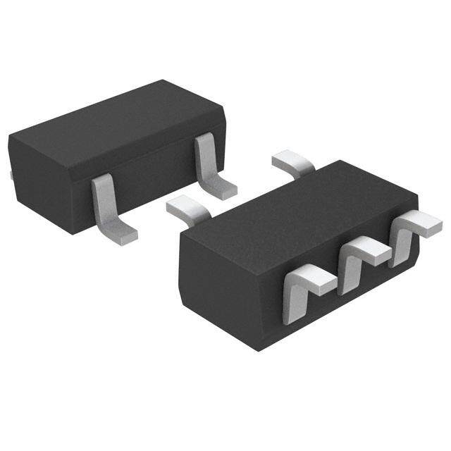
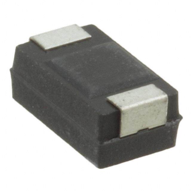
| 描述 | TRANS DUAL PNP 50V 100MA SOT963 |
| 产品分类 | 晶体管(BJT) - 阵列 |
| 品牌 | Diodes Incorporated |
| 数据手册 | |
| 产品图片 |
|
| 产品型号 | DP0150ADJ-7 |
| rohs | 无铅 / 符合限制有害物质指令(RoHS)规范要求 |
| RoHS指令信息 | http://diodes.com/download/4349 |
| 产品系列 | - |
| 不同 Ib、Ic时的 Vce饱和值(最大值) | 300mV @ 10mA,100mA |
| 不同 Ic、Vce 时的DC电流增益(hFE)(最小值) | 120 @ 2mA,6V |
| 供应商器件封装 | SOT-963 |
| 其它名称 | DP0150ADJ-7DICT |
| 功率-最大值 | 300mW |
| 包装 | 剪切带 (CT) |
| 安装类型 | 表面贴装 |
| 封装/外壳 | SOT-963 |
| 晶体管类型 | 2 PNP(双) |
| 标准包装 | 1 |
| 电压-集射极击穿(最大值) | 50V |
| 电流-集电极(Ic)(最大值) | 100mA |
| 电流-集电极截止(最大值) | - |
| 频率-跃迁 | 80MHz |


PDF Datasheet 数据手册内容提取
DP0150ADJ / DP0150BDJ DUAL PNP SURFACE MOUNT TRANSISTOR Features Mechanical Data • Epitaxial Planar Die Construction • Case: SOT-963 • Ideally Suited for Automated Assembly Processes • Case Material: Molded Plastic, “Green” Molding Compound. UL • Lead Free By Design/RoHS Compliant (Note 1) Flammability Classification Rating 94V-0 • "Green" Device (Note 2) • Moisture Sensitivity: Level 1 per J-STD-020D T • Ultra Small Package • Terminals: Finish ⎯ Matte Tin annealed over Copper leadframe. C Solderable per MIL-STD-202, Method 208 U • Marking Information: See Page 3 D • Ordering Information: See Page 3 O • Weight: 0.0027 grams (approximate) R SOT-963 P 6 5 4 W E Q1 Q2 N 1 2 3 Top View Device Schematic Maximum Ratings @TA = 25°C unless otherwise specified Characteristic Symbol Value Unit Collector-Base Voltage VCBO -50 V Collector-Emitter Voltage VCEO -50 V Emitter-Base Voltage VEBO -5 V Collector Current - Continuous IC -100 mA Base Current IB -30 mA Thermal Characteristics Characteristic Symbol Value Unit Power Dissipation (Note 3) PD 300 mW Thermal Resistance, Junction to Ambient (Note 3) RθJA 417 °C/W Operating and Storage Temperature Range TJ, TSTG -55 to +150 °C Electrical Characteristics @TA = 25°C unless otherwise specified Characteristic Symbol Min Typ Max Unit Test Condition OFF CHARACTERISTICS (Note 4) Collector-Base Breakdown Voltage V(BR)CBO -50 — — V IC = -10μA, IE = 0 Collector-Emitter Breakdown Voltage V(BR)CEO -50 — — V IC = -1mA, IB = 0 Emitter-Base Breakdown Voltage V(BR)EBO -5 — — V IE = -10μA, IC = 0 Collector Cut-Off Current ICBO — — -0.1 μA VCB = -50V, IE = 0 Emitter Cut-Off Current IEBO — — -0.1 μA VEB = -5V, IC = 0 ON CHARACTERISTICS (Note 4) Collector-Emitter Saturation Voltage VCE(SAT) — -0.15 -0.3 V IC = -100mA, IB = -10mA DC Current Gain DP0150ADJ 120 — 240 DP0150BDJ hFE 200 — 400 — VCE = -6V, IC = -2mA SMALL SIGNAL CHARACTERISTICS Transition Frequency fT 80 — — MHz Vf =C E3 0=M -1H0zV , IE = 1mA Output Capactiance Cob — 1.6 — pF fV =C B1 M= H-1z0 V, IE = 0, Notes: 1. No purposefully added lead. 2. Diodes Inc.'s "Green" policy can be found on our website at http://www.diodes.com/products/lead_free/index.php. 3. Device mounted on FR-4 PCB with minimum recommended pad layout. 4. Measured under pulsed conditions. Pulse width = 300µs. Duty cycle ≤2% DP0150ADJ / DP0150BDJ 1 of 4 April 2009 Document number: DS31485 Rev. 3 - 2 www.diodes.com © Diodes Incorporated
DP0150ADJ / DP0150BDJ 300 1,000 250 A) N (W) NT (m TIO 200 RRE 100 Pw = 10ms PA U T SSI 150 R C C DI TO Pw = 100ms U R C D WE 100 LLE 10 DC O O O P C R , D , C P P 50 RθJA = 417°C/W -I W E 0 1 N 0 25 50 75 100 125 150 0.1 1 10 100 TA, AMBIENT TEMPERATURE (°C) -VCE, CFOigL. L2E TCyTpOicRal- ECMolIlTecTtEoRr C VuOrrLeTnAtGE (V) Fig. 1 Power Dissipation vs. Ambient Temperature (Note 3) vs. Collector-Emitter Voltage (Note 3) 1,000 1 TA = 150°C R IC/IB = 10 E TV) N TA = 85°C MITE ( AI TA = 25°C EG T G OR-LTA CURREN100 TA = -55°C OLLECTVOTION 0.1 TA =T 8A5 =°C 150°C DC , CT)URA TA = 25°C h, FE CE(SASAT TA = -55°C V - VCE = -6V 10 0.01 0.1 1 10 100 1,000 0.0001 0.001 0.01 0.1 1 -I , COLLECTOR CURRENT (mA) -I , COLLECTOR CURRENT (A) C C Fig. 3 Typical DC Current Gain Fig. 4 Typical Collector-Emitter Saturation Voltage vs. Collector Current (DN0150BDJ) vs. Collector Current V) 1.2 V) 1.2 E ( E ( G G LTA 1.0 VCE = -6V LTA 1.0 IC/IB = 10 O O V V N N O 0.8 O RN- TA = -55°C RATI 0.8 U U TA = -55°C R T 0.6 AT EMITTE 0.4 TTAA == 8255°°CC TTER S 0.6 TA = 25°C E- MI BAS 0.2 TA = 150°C SE-E 0.4 TA = 85°C , N) BA BE(O 0 , AT)0.2 TA = 150°C V S - 0.0001 0.001 0.01 0.1 1 E( 0.0001 0.001 0.01 0.1 1 B -I , COLLECTOR CURRENT (A) V -I , COLLECTOR CURRENT (A) C - C Fig. 5 Typical Base-Emitter Turn-On Voltage Fig. 6 Typical Base-Emitter Saturation Voltage vs. Collector Current vs. Collector Current DP0150ADJ / DP0150BDJ 2 of 4 April 2009 Document number: DS31485 Rev. 3 - 2 www.diodes.com © Diodes Incorporated
DP0150ADJ / DP0150BDJ 100 250 f = 1MHz z) H 200 M F) 10 CT ( p U UCT TANCE ( Cibo H PROD 150 CI T D A D 100 P WI O CA 1 Cobo D R N A P B W AIN- 50 fV =C E3 0=M -6HVz G E , T N 0 f 0 0.1 1 10 100 0 2 4 6 8 10 V , REVERSE VOLTAGE (V) -I , COLLECTOR CURRENT (mA) R C Fig. 7 Typical Capacitance Characteristics Fig. 8 Typical Gain-Bandwidth Product vs. Collector Current Ordering Information (Note 5) Device Packaging Shipping DP0150ADJ-7 SOT-963 10,000/Tape & Reel DP0150BDJ-7 SOT-963 10,000/Tape & Reel Notes: 5. For packaging details, go to our website at http://www.diodes.com/datasheets/ap02007.pdf. Marking Information xx= Product Type Marking Code: xx T5 = DP0150ADJ T6 = DP0150BDJ Package Outline Dimensions D e1 L SOT-963 Dim Min Max Typ A 0.40 0.50 0.45 E1 E A1 0 0.05 - c 0.077 0.177 0.127 D 0.95 1.05 1.00 E 0.95 1.05 1.00 E1 0.75 0.85 0.80 e b (5 places) c L 0.05 0.15 0.10 b 0.10 0.20 0.15 e 0.35 Typ e1 0.70 Typ A All Dimensions in mm A1 DP0150ADJ / DP0150BDJ 3 of 4 April 2009 Document number: DS31485 Rev. 3 - 2 www.diodes.com © Diodes Incorporated
DP0150ADJ / DP0150BDJ IMPORTANT NOTICE DIODES INCORPORATED MAKES NO WARRANTY OF ANY KIND, EXPRESS OR IMPLIED, WITH REGARDING TO THIS DOCUMENT, INCLUDING, BUT NOT LIMITED TO, THE IMPLIED WARRANTIES OF MERCHANTABILITY AND FITNESS FOR A PARTICULAR PURPOSE (AND THEIR EQUIVALENTS UNDER THE LAWS OF ANY JURISDICTION). T Diodes Incorporated and its subsidiaries reserve the right to make modifications, enhancements, improvements, corrections or other changes C without further notice to this document and any product described herein. Diodes Incorporated does not assume any liability arising out of the application or use of this document or any product described herein; neither does Diodes Incorporated convey any license under its patent or U trademark rights, nor the rights of others. Any Customer or user of this document or products described herein in such applications shall assume D all risks of such use and will agree to hold Diodes Incorporated and all the companies whose products are represented on Diodes Incorporated O website, harmless against all damages. R P Diodes Incorporated does not warrant or accept any liability whatsoever in respect of any products purchased through unauthorized sales channel. Should Customers purchase or use Diodes Incorporated products for any unintended or unauthorized application, Customers shall indemnify and W hold Diodes Incorporated and its representatives harmless against all claims, damages, expenses, and attorney fees arising out of, directly or E indirectly, any claim of personal injury or death associated with such unintended or unauthorized application. N Products described herein may be covered by one or more United States, international or foreign patents pending. Product names and markings noted herein may also be covered by one or more United States, international or foreign trademarks. LIFE SUPPORT Diodes Incorporated products are specifically not authorized for use as critical components in life support devices or systems without the express written approval of the Chief Executive Officer of Diodes Incorporated. As used herein: A. Life support devices or systems are devices or systems which: 1. are intended to implant into the body, or 2. support or sustain life and whose failure to perform when properly used in accordance with instructions for use provided in the labeling can be reasonably expected to result in significant injury to the user. B. A critical component is any component in a life support device or system whose failure to perform can be reasonably expected to cause the failure of the life support device or to affect its safety or effectiveness. Customers represent that they have all necessary expertise in the safety and regulatory ramifications of their life support devices or systems, and acknowledge and agree that they are solely responsible for all legal, regulatory and safety-related requirements concerning their products and any use of Diodes Incorporated products in such safety-critical, life support devices or systems, notwithstanding any devices- or systems-related information or support that may be provided by Diodes Incorporated. Further, Customers must fully indemnify Diodes Incorporated and its representatives against any damages arising out of the use of Diodes Incorporated products in such safety-critical, life support devices or systems. Copyright © 2009, Diodes Incorporated www.diodes.com DP0150ADJ / DP0150BDJ 4 of 4 April 2009 Document number: DS31485 Rev. 3 - 2 www.diodes.com © Diodes Incorporated
Mouser Electronics Authorized Distributor Click to View Pricing, Inventory, Delivery & Lifecycle Information: D iodes Incorporated: DP0150ADJ-7