ICGOO在线商城 > 集成电路(IC) > PMIC - PFC(功率因数修正) > UCC28513N

 Datasheet下载
- 型号: UCC28513N
- 制造商: Texas Instruments
- 库位|库存: xxxx|xxxx
- 要求:
| 数量阶梯 | 香港交货 | 国内含税 |
| +xxxx | $xxxx | ¥xxxx |
查看当月历史价格
查看今年历史价格
UCC28513N产品简介:
ICGOO电子元器件商城为您提供UCC28513N由Texas Instruments设计生产,在icgoo商城现货销售,并且可以通过原厂、代理商等渠道进行代购。 UCC28513N价格参考¥17.67-¥32.83。Texas InstrumentsUCC28513N封装/规格:PMIC - PFC(功率因数修正), PFC IC Average Current 200kHz 20-PDIP。您可以下载UCC28513N参考资料、Datasheet数据手册功能说明书,资料中有UCC28513N 详细功能的应用电路图电压和使用方法及教程。
UCC28513N 是 Texas Instruments(德州仪器)推出的一款用于功率因数校正(PFC)的电源管理 IC,属于固定频率、电流模式控制的升压型 PFC 控制器。它主要应用于需要高功率因数和低总谐波失真的交流-直流(AC-DC)电源转换系统中。

该器件常见于以下应用场景:

1. 工业电源系统:如工业用开关电源、UPS(不间断电源)系统中,用于提高输入功率因数,减少对电网的谐波污染。

2. 服务器和电信电源:在高可靠性、高效率要求的数据中心服务器电源和通信设备电源中,UCC28513N 可有效提升能效并满足国际电磁兼容(EMC)标准。

3. 家电电源:如高端变频空调、洗衣机等家电产品中的电源模块,用于实现高效能电能转换。

4. LED 照明驱动:在高功率 LED 照明系统中,作为前级 PFC 转换器,确保系统符合电力质量规范。

5. 消费类电子产品适配器:如笔记本电脑、高性能音响等设备的电源适配器中,用于提升功率因数并减小输入电流谐波。

UCC28513N 采用 8 引脚 PDIP 或 SOIC 封装,具备低启动电流、可调开关频率、过压保护等功能,适合中高功率应用场合。其设计灵活,便于实现高效率、高稳定性的 PFC 电路。
| 参数 | 数值 |
| 产品目录 | 集成电路 (IC)半导体 |
| 描述 | IC PFC/PWM COMB CTRLR 20-DIP功率因数校正 - PFC Advanced PFC/PWM Comb Controller |
| 产品分类 | |
| 品牌 | Texas Instruments |
| 产品手册 | |
| 产品图片 |
|
| rohs | 符合RoHS无铅 / 符合限制有害物质指令(RoHS)规范要求 |
| 产品系列 | 电源管理 IC,功率因数校正 - PFC,Texas Instruments UCC28513N- |
| 数据手册 | |
| 产品型号 | UCC28513N |
| PCN设计/规格 | |
| 产品目录页面 | |
| 产品种类 | 功率因数校正 - PFC |
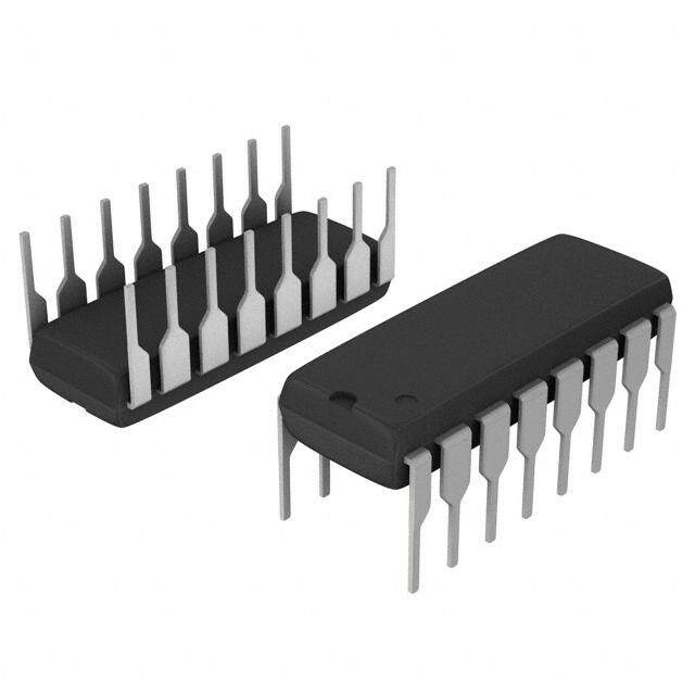
| 供应商器件封装 | 20-PDIP |
| 其它名称 | 296-14225-5 |
| 包装 | 管件 |
| 单位重量 | 1.199 g |
| 商标 | Texas Instruments |
| 安装类型 | 通孔 |
| 安装风格 | Through Hole |
| 封装 | Tube |
| 封装/外壳 | 20-DIP(0.300",7.62mm) |
| 封装/箱体 | PDIP-20 |
| 工作温度 | -40°C ~ 105°C |
| 工厂包装数量 | 20 |
| 开关频率 | 230 kHz |
| 最大工作温度 | + 105 C |
| 最小工作温度 | - 40 C |
| 标准包装 | 20 |
| 模式 | 平均电流 |
| 电压-电源 | 9.7 V ~ 18 V |
| 电流-启动 | 100µA |
| 系列 | UCC28513 |
| 配用 | /product-detail/zh/UCC28514EVM/296-19040-ND/863861 |
| 频率-开关 | 200kHz |


- 商务部:美国ITC正式对集成电路等产品启动337调查
- 曝三星4nm工艺存在良率问题 高通将骁龙8 Gen1或转产台积电
- 太阳诱电将投资9.5亿元在常州建新厂生产MLCC 预计2023年完工
- 英特尔发布欧洲新工厂建设计划 深化IDM 2.0 战略
- 台积电先进制程称霸业界 有大客户加持明年业绩稳了
- 达到5530亿美元!SIA预计今年全球半导体销售额将创下新高
- 英特尔拟将自动驾驶子公司Mobileye上市 估值或超500亿美元
- 三星加码芯片和SET,合并消费电子和移动部门,撤换高东真等 CEO
- 三星电子宣布重大人事变动 还合并消费电子和移动部门
- 海关总署:前11个月进口集成电路产品价值2.52万亿元 增长14.8%


PDF Datasheet 数据手册内容提取
(cid:1)(cid:2)(cid:2)(cid:3)(cid:4)(cid:5)(cid:6)(cid:7)(cid:8) (cid:1)(cid:2)(cid:2)(cid:3)(cid:4)(cid:5)(cid:6)(cid:6)(cid:8) (cid:1)(cid:2)(cid:2)(cid:3)(cid:4)(cid:5)(cid:6)(cid:3)(cid:8) (cid:1)(cid:2)(cid:2)(cid:3)(cid:4)(cid:5)(cid:6)(cid:9)(cid:8) (cid:1)(cid:2)(cid:2)(cid:3)(cid:4)(cid:5)(cid:6)(cid:10)(cid:8) (cid:1)(cid:2)(cid:2)(cid:3)(cid:4)(cid:5)(cid:6)(cid:5)(cid:8) (cid:1)(cid:2)(cid:2)(cid:3)(cid:4)(cid:5)(cid:6)(cid:11)(cid:8) (cid:1)(cid:2)(cid:2)(cid:3)(cid:4)(cid:5)(cid:6)(cid:12) SLUS517C − DECEMBER 2002 − REVISED SEPTEMBER 2005 (cid:13)(cid:14)(cid:15)(cid:13)(cid:16)(cid:2)(cid:17)(cid:14) (cid:18)(cid:19)(cid:2)(cid:20)(cid:18)(cid:21)(cid:22) (cid:2)(cid:23)(cid:22)(cid:24)(cid:25)(cid:16)(cid:13)(cid:26)(cid:25)(cid:23)(cid:16) (cid:2)(cid:23)(cid:16)(cid:26)(cid:27)(cid:23)(cid:28)(cid:28)(cid:17)(cid:27)(cid:29) FEATURES DESCRIPTION (cid:1) Provides Control of PFC and PWM Power The UCC28510 series of combination PFC/PWM Stages In One Device controllers provide complete control functionality (cid:1) for any off-line power system requiring Leading-Edge PFC, Trailing-Edge PWM compliance with the IEC1000−3−2 harmonic Modulation for Reduced Ripple reduction requirements. By combining the control (cid:1) Built-In Sequencing of PFC and PWM and drive signals for the PFC and the PWM stages Turn-On into a single device, significant performance and (cid:1) 2-A Source and 3-A Sink Gate Drive for Both cost benefits are gained. By managing the PFC and PWM Stages modulation mechanisms of the two stages (cid:1) Typical 16-ns Rise Time and 7-ns Fall Time (leading-edge modulation for PFC and into 1-nF Loads trailing-edge modulation for PWM), the ripple current in the boost capacitor is minimized. PFC Features Based on the average current mode control − Average-Current-Mode Control for architecture with input voltage feedforward of prior Continuous Conduction Mode Operation PFC/PWM combination controllers, these devices − Highly-Linear Multiplier for Near-Unity offer performance advantages. Two new key Power Factor PWM features are programmable maximum duty − Input Voltage Feedforward Implementation cycle and the 2x PWM frequency options to the − Improved Load Transient Response base PFC frequency. For the PFC stage, the − Accurate Power Limiting devices feature an improved multiplier and the − Zero Power Detect use of a transconductance amplifier for enhanced PWM Features transient response. − Peak-Current-Mode Control Operation The core of the PFC section is in a three-input − 1:1 or 1:2 PFC:PWM Frequency Options multiplier that generates the reference signal for − Programmable maximum duty cycle the line current. The UCC28510 series features a − Programmable Soft-Start highly linearized multiplier circuit capable of − Two Hysteresis Options for Differing producing a low distortion reference for the line Hold-Up Time Requirements current over the full range of line and load conditions. A low-offset, high-bandwidth current error amplifier ensures that the actual inductor current (sensed through a resistor in the return path) follows the multiplier output command signal. The output voltage error is processed through a transconductance voltage amplifier. (cid:18)(cid:27)(cid:23)(cid:14)(cid:1)(cid:2)(cid:26)(cid:25)(cid:23)(cid:16) (cid:14)(cid:13)(cid:26)(cid:13) (cid:30)(cid:31)!"#$%&(cid:30)"(cid:31) (cid:30)’ ()##*(cid:31)& %’ "! +),-(cid:30)(%&(cid:30)"(cid:31) .%&*/ Copyright 2004, Texas Instruments Incorporated (cid:18)#".)(&’ ("(cid:31)!"#$ &" ’+*((cid:30)!(cid:30)(%&(cid:30)"(cid:31)’ +*# &0* &*#$’ "! (cid:26)*1%’ (cid:25)(cid:31)’&#)$*(cid:31)&’ ’&%(cid:31).%#. 2%##%(cid:31)&3/ (cid:18)#".)(&(cid:30)"(cid:31) +#"(*’’(cid:30)(cid:31)4 ."*’ (cid:31)"& (cid:31)*(*’’%#(cid:30)-3 (cid:30)(cid:31)(-).* &*’&(cid:30)(cid:31)4 "! %-- +%#%$*&*#’/ www.ti.com 1
(cid:1)(cid:2)(cid:2)(cid:3)(cid:4)(cid:5)(cid:6)(cid:7)(cid:8) (cid:1)(cid:2)(cid:2)(cid:3)(cid:4)(cid:5)(cid:6)(cid:6)(cid:8) (cid:1)(cid:2)(cid:2)(cid:3)(cid:4)(cid:5)(cid:6)(cid:3)(cid:8) (cid:1)(cid:2)(cid:2)(cid:3)(cid:4)(cid:5)(cid:6)(cid:9)(cid:8) (cid:1)(cid:2)(cid:2)(cid:3)(cid:4)(cid:5)(cid:6)(cid:10)(cid:8) (cid:1)(cid:2)(cid:2)(cid:3)(cid:4)(cid:5)(cid:6)(cid:5)(cid:8) (cid:1)(cid:2)(cid:2)(cid:3)(cid:4)(cid:5)(cid:6)(cid:11)(cid:8) (cid:1)(cid:2)(cid:2)(cid:3)(cid:4)(cid:5)(cid:6)(cid:12) SLUS517C − DECEMBER 2002 − REVISED SEPTEMBER 2005 DESCRIPTION (CONTINUED) The transient response of the circuit is enhanced by allowing a much faster charge/discharge of the voltage amplifier output capacitance when the output voltage falls outside a certain regulation window. A number of additional features such as UVLO circuit with selectable hysteresis levels, an accurate reference voltage for the voltage amplifier, zero power detect, OVP/enable, peak current limit, power limiting, high-current output gate driver characterize the PFC section. The PWM section features peak current mode control (with a ramp signal available to add slope compensation), programmable soft-start, accurate maximum duty cycle clamp, peak current limit and high-current output gate driver. The oscillator for the combination controller is available in two versions. In UCC28510, UCC28511, UCC28512, and UCC28513, the PWM and the PFC circuits are switched at the same frequency. In the UCC28514, UCC28515, UCC28516, and UCC28517, the PWM stage frequency is twice that of the PFC frequency. The PWM stage is suppressed until the PFC output has reached 90% of its programmed value during startup. During line dropout and turn off, the device allows the PWM stage to operate until the PFC output has dropped to 47% (UCC28512, UCC28513, UCC28516, and UCC28517) or 71% (UCC28510, UCC28511, UCC28514, and UCC28515) of its nominal value. See available options table on page 1 for a summary of options. The UCC28510 family also features leading-edge modulation for the PFC stage and trailing-edge modulation for the PWM stage in order to reduce the ripple current in the boost output capacitor. The current amplifier implementation associated with this scheme also results in better noise immunity. Available in 20-pin N and DW packages. SIMPLIFIED APPLICATION DIAGRAM PRIMARY SECONDARY + RECT VOUT + D1 − − VAC + BIAS UCC2851X − 11 PWRGND GT2 10 REF 12 GT1 VCC 9 13 SS2 ISENSE2 8 14 PKLMT VERR 7 15 CAOUT GND 6 Z 16 ISENSE1 CT_BUFF 5 17 MOUT D_MAX 4 PWM + V−LOOP 18 IAC VSENSE 3 19 VFF RT 2 20 VREF VAOUT 1 Z REF Z 2 www.ti.com
(cid:1)(cid:2)(cid:2)(cid:3)(cid:4)(cid:5)(cid:6)(cid:7)(cid:8) (cid:1)(cid:2)(cid:2)(cid:3)(cid:4)(cid:5)(cid:6)(cid:6)(cid:8) (cid:1)(cid:2)(cid:2)(cid:3)(cid:4)(cid:5)(cid:6)(cid:3)(cid:8) (cid:1)(cid:2)(cid:2)(cid:3)(cid:4)(cid:5)(cid:6)(cid:9)(cid:8) (cid:1)(cid:2)(cid:2)(cid:3)(cid:4)(cid:5)(cid:6)(cid:10)(cid:8) (cid:1)(cid:2)(cid:2)(cid:3)(cid:4)(cid:5)(cid:6)(cid:5)(cid:8) (cid:1)(cid:2)(cid:2)(cid:3)(cid:4)(cid:5)(cid:6)(cid:11)(cid:8) (cid:1)(cid:2)(cid:2)(cid:3)(cid:4)(cid:5)(cid:6)(cid:12) SLUS517C − DECEMBER 2002 − REVISED SEPTEMBER 2005 ABSOLUTE MAXIMUM RATINGS over operating free-air temperature (unless otherwise noted)†(cid:2) Supply voltage VCC Idle . . . . . . . . . . . . . . . . . . . . . . . . . . . . . . . . . . . . . . . . . . . . . . . . . . . . . . . . . . . . . . . . . . . . . . . . . . . . . . . . . . 20 V Operating . . . . . . . . . . . . . . . . . . . . . . . . . . . . . . . . . . . . . . . . . . . . . . . . . . . . . . . . . . . . . . . . . . . . . . . . . . . . . 18 V Gate drive current (GT1, GT2) Continuous . . . . . . . . . . . . . . . . . . . . . . . . . . . . . . . . . . . . . . . . . . . . . . . . . . . . . . . . . . . . . . . . . . . . . . . . . . 0.4 A Pulsed Sourcing . . . . . . . . . . . . . . . . . . . . . . . . . . . . . . . . . . . . . . . . . . . . . . . . . . . . . . . . . . . . . . . . . . . . −2.5 A Sinking . . . . . . . . . . . . . . . . . . . . . . . . . . . . . . . . . . . . . . . . . . . . . . . . . . . . . . . . . . . . . . . . . . . . . . . 3.5 A Maximum GT1, GT2 voltage . . . . . . . . . . . . . . . . . . . . . . . . . . . . . . . . . . . . . . . . . . . . . . . . . . −0.5 V to VCC+0.3 V Input voltage VSENSE . . . . . . . . . . . . . . . . . . . . . . . . . . . . . . . . . . . . . . . . . . . . . . . . . . . . . . . . . . . . . . . . . . . . . . . 0 V to 11 V D_MAX, SS2, CAOUT, ISENSE1, MOUT, VFF. . . . . . . . . . . . . . . . . . . . . . . . . . . . . −0.5 V to VREF+0.3 V VAOUT, CT_BUFF, ISENSE2, PKLMT . . . . . . . . . . . . . . . . . . . . . . . . . . . . . . . . . . . . . . . . . . . . −0.5 V to 6 V Pin Current RT . . . . . . . . . . . . . . . . . . . . . . . . . . . . . . . . . . . . . . . . . . . . . . . . . . . . . . . . . . . . . . . . . . . . . . . . . . . . . . . . −0.5 mA VFF . . . . . . . . . . . . . . . . . . . . . . . . . . . . . . . . . . . . . . . . . . . . . . . . . . . . . . . . . . . . . . . . . . . . . . . . . . . . . . . . −5 mA CT_BUFF . . . . . . . . . . . . . . . . . . . . . . . . . . . . . . . . . . . . . . . . . . . . . . . . . . . . . . . . . . . . . . . . . . . . . . . . . . . 1 mA VAOUT, VERR, ISENSE2, SS2, CAOUT, IAC . . . . . . . . . . . . . . . . . . . . . . . . . . . . . . . . . . . . . . . . . . . 10 mA Maximum pin capacitance ISENSE2 . . . . . . . . . . . . . . . . . . . . . . . . . . . . . . . . . . . . . . . . . . . . . . . . . . . . . . . . . . . . . . . . . . . . . . . . . . . 220 pF Operating junction temperature range, T . . . . . . . . . . . . . . . . . . . . . . . . . . . . . . . . . . . . . . . . . . −55 0C to 150 0C J Storage Temperature range, T . . . . . . . . . . . . . . . . . . . . . . . . . . . . . . . . . . . . . . . . . . . . . . . . . −65 0C to 150 0C stg Lead temperature 1.6mm (1/16 inch from case for 10 seconds) . . . . . . . . . . . . . . . . . . . . . . . . . . . . . . . . . 300 0C Power dissipation PDIP (N) package . . . . . . . . . . . . . . . . . . . . . . . . . . . . . . . . . . . . . . . . . . . . . . . . . . . . . . . . . . . . . . . . . . . . . 1 W SOIC (DW) package . . . . . . . . . . . . . . . . . . . . . . . . . . . . . . . . . . . . . . . . . . . . . . . . . . . . . . . . . . . . . . . . . . 0.7 W †Stresses beyond those listed under “absolute maximum ratings” may cause permanent damage to the device. These are stress ratings only, and functional operation of the device at these or any other conditions beyond those indicated under recommended operating conditions is not implied. Exposure to absolute−maximum−rated conditions for extended periods may affect reliability. ‡Currents are positive into, negative out of the specified terminal. All voltages are referenced to GND. ELECTROSTATIC DISCHARGE (ESD) PROTECTION PARAMETER MAX UNITS Human body model 2.5 kkVV CDM 0.5 AVAILABLE OPTIONS(cid:1)(cid:2) OPTIONS PACKAGED DEVICES PFC:PWM UVLO UVLO PWM UVLO2 PWM UVLO2 PDIP−20 SOIC W−20 FREQUENCY TURN-ON (V) HYSTERESIS (V) TURN-OFF (V) HYSTERESIS (V) (N) (DW) RATIO 1:1 16 6.3 5.30 1.45 UCC28510N UCC28510DW 1:1 10.2 0.5 5.30 1.45 UCC28511N UCC28511DW 1:1 16 6.3 3.55 3.2 UCC28512N UCC28512DW 1:1 10.2 0.5 3.55 3.2 UCC28513N UCC28513DW 1:2 16 6.3 5.30 1.45 UCC28514N UCC28514DW 1:2 10.2 0.5 5.30 1.45 UCC28515N UCC28515DW 1:2 16 6.3 3.55 3.2 UCC28516N UCC28516DW 1:2 10.2 0.5 3.55 3.2 UCC28517N UCC28517DW †The DW package is available taped and reeled. Add R suffix to device type (e.g. UCC28510DWR) to order quantities of 2000 devices per reel. ‡All devices are rated from −40°C to +105°C. www.ti.com 3
(cid:1)(cid:2)(cid:2)(cid:3)(cid:4)(cid:5)(cid:6)(cid:7)(cid:8) (cid:1)(cid:2)(cid:2)(cid:3)(cid:4)(cid:5)(cid:6)(cid:6)(cid:8) (cid:1)(cid:2)(cid:2)(cid:3)(cid:4)(cid:5)(cid:6)(cid:3)(cid:8) (cid:1)(cid:2)(cid:2)(cid:3)(cid:4)(cid:5)(cid:6)(cid:9)(cid:8) (cid:1)(cid:2)(cid:2)(cid:3)(cid:4)(cid:5)(cid:6)(cid:10)(cid:8) (cid:1)(cid:2)(cid:2)(cid:3)(cid:4)(cid:5)(cid:6)(cid:5)(cid:8) (cid:1)(cid:2)(cid:2)(cid:3)(cid:4)(cid:5)(cid:6)(cid:11)(cid:8) (cid:1)(cid:2)(cid:2)(cid:3)(cid:4)(cid:5)(cid:6)(cid:12) SLUS517C − DECEMBER 2002 − REVISED SEPTEMBER 2005 ELECTRICAL CHARACTERISTICS T = –40°C to 105°C for the UCC2851x, T = T , VCC = 12 V, R = 156 kΩ, R = 10 kΩ A A J T CT_BUFF (unless otherwise noted) supply current PARAMETER TEST CONDITIONS MIN TYP MAX UNITS Supply current, off VCC turn-on threshold −300 mV 100 150 µA Supply current, on no load on GT1 or GT2 4 6 mA undervoltage lockout (UVLO) PARAMETER TEST CONDITIONS MIN TYP MAX UNITS UCC28510 UCC28512 15.4 16 16.6 UCC28514 UCC28516 VVCCCC ttuurrnn--oonn tthhrreesshhoolldd UCC28511 UCC28513 9.7 10.2 10.8 UCC28515 UCC28517 VCC turn-off threshold UCC2851X 9.1 9.7 10.6 VV UCC28510 UCC28512 5.8 6.3 6.8 UCC28514 UCC28516 UUVVLLOO hhyysstteerreessiiss UCC28511 UCC28513 0.3 0.5 0.8 UCC28515 UCC28517 voltage amplifier PARAMETER TEST CONDITIONS MIN TYP MAX UNITS 25°C 7.39 7.50 7.61 IInnppuutt vvoollttaaggee VV Over temperature 7.35 7.50 7.65 VSENSE bias current VSENSE = VREF 100 300 nA Open loop gain 2 V ≤ VAOUT ≤ 4 V 50 60 dB High-level output voltage ILOAD = –150 µA 5.3 5.5 5.6 VV Low-level output voltage ILOAD = 150 µA 0.00 0.05 0.15 gM conductance IVAOUT = −20 µA to 20 µA 70 100 130 µS Maximum source current −1 −3.5 mmAA Maximum sink current 1 3.5 PFC stage overvoltage protection and enable PARAMETER TEST CONDITIONS MIN TYP MAX UNITS VREF VREF VREF Overvoltage reference window V + 0.440 + 0.490 + 0.540 Hysteresis 300 500 600 mV Enable threshold 1.7 1.9 2.1 VV Enable hysteresis 0.08 0.2 0.3 4 www.ti.com
(cid:1)(cid:2)(cid:2)(cid:3)(cid:4)(cid:5)(cid:6)(cid:7)(cid:8) (cid:1)(cid:2)(cid:2)(cid:3)(cid:4)(cid:5)(cid:6)(cid:6)(cid:8) (cid:1)(cid:2)(cid:2)(cid:3)(cid:4)(cid:5)(cid:6)(cid:3)(cid:8) (cid:1)(cid:2)(cid:2)(cid:3)(cid:4)(cid:5)(cid:6)(cid:9)(cid:8) (cid:1)(cid:2)(cid:2)(cid:3)(cid:4)(cid:5)(cid:6)(cid:10)(cid:8) (cid:1)(cid:2)(cid:2)(cid:3)(cid:4)(cid:5)(cid:6)(cid:5)(cid:8) (cid:1)(cid:2)(cid:2)(cid:3)(cid:4)(cid:5)(cid:6)(cid:11)(cid:8) (cid:1)(cid:2)(cid:2)(cid:3)(cid:4)(cid:5)(cid:6)(cid:12) SLUS517C − DECEMBER 2002 − REVISED SEPTEMBER 2005 ELECTRICAL CHARACTERISTICS T = –40°C to 105°C for the UCC2851x, T = T , VCC = 12 V, R = 156 kΩ, R = 10 kΩ A A J T CT_BUFF (unless otherwise noted) current amplifier PARAMETER TEST CONDITIONS MIN TYP MAX UNITS Input offset voltage VCM = 0 V, VCAOUT = 3 V –5 0 5 mV Input bias current VCM = 0 V, VCAOUT = 3 V −50 −100 nnAA Input offset current VCM = 0 V, VCAOUT = 3 V 25 100 Open loop gain VCM = 0 V, 2 V ≤ VCAOUT ≤ 5 V 90 ddBB Common−mode rejection ratio 0 V ≤ VCM ≤ 1.5 V, VCAOUT = 3 V 80 High-level output voltage ILOAD = –500 µA 5.6 6.3 7.0 VV Low-level output voltage ILOAD = 500 µA 0 0.2 0.5 Gain bandwidth product(1) See Note 1 2.0 MHz oscillator PARAMETER TEST CONDITIONS MIN TYP MAX UNITS fPWM, PWM frequency, initial accuracy TA = 25°C 170 200 230 kHz Frequency, voltage stability 10.8 V ≤ VCC ≤ 15 V −1% 1% Frequency, total variation Line, Temp 160 240 kHz dc-to-dc ramp peak voltage 4.5 5.0 5.5 dc-to-dc ramp amplitude voltage(1) 4.0 (peak-to-peak) VV PFC ramp peak voltage 4.5 5.0 5.5 PFC ramp amplitude voltage (peak-to-peak) 3.5 4.0 4.5 voltage reference PARAMETER TEST CONDITIONS MIN TYP MAX UNITS 25°C 7.39 7.50 7.61 V IInnppuutt vvoollttaaggee Over temperature 7.35 7.50 7.65 V Load regulation IREF = −1 mA to −6 mA 5 15 mmVV Line regulation 10.8 V ≤ VCC ≤ 15 V 1 10 Short circuit current VREF = 0V −20 –25 −50 mA peak current limit PARAMETER TEST CONDITIONS MIN TYP MAX UNITS PKLMT reference voltage –20 0 20 mV PKLMT propagation delay PKLMT to GT1 150 300 500 ns multiplier PARAMETER TEST CONDITIONS MIN TYP MAX UNITS IMOUT, high-line low-power output current IAC = 500 µA, VFF = 4.7 V, VAOUT = 1.25 V −3 –6 −9 IMOUT, high-line high-power output current IAC = 500 µA, VFF = 4.7 V, VAOUT = 5 V −75 –90 −110 IMOUT, low-line low-power output current IAC = 150 µA, VFF = 1.4 V, VAOUT = 1.25 V −10 –15 −50 µµAA IMOUT, low-line high-power output current IAC = 150 µA, VFF = 1.4 V, VAOUT = 5 V −245 –290 −330 IMOUT, IAC-limited output current IAC = 150 µA, VFF = 1.3 V, VAOUT = 5 V −245 –290 −330 Gain constant (k) IAC = 300 µA, VFF = 2.8 V, VAOUT = 2.5 V 0.8 1 1.2 1/V IAC = 150 µA, VFF = 1.4 V, VAOUT = 0.25 V 0 –0.2 µA IIMMOOUUTT,, zzeerroo ccuurrrreenntt IAC = 500 µA, VFF = 4.7 V, VAOUT = 0.25 V 0 –0.2 µA IAC = 500 µA, VFF = 4.7 V, VAOUT = 0.5 V 0 –0.2 µA Power limit (IMOUT × VFF) IAC = 150 µA, VFF = 1.4 V, VAOUT = 5 V −343 –406 −462 µW 1. Ensured by design. Not 100% tested in production. www.ti.com 5
(cid:1)(cid:2)(cid:2)(cid:3)(cid:4)(cid:5)(cid:6)(cid:7)(cid:8) (cid:1)(cid:2)(cid:2)(cid:3)(cid:4)(cid:5)(cid:6)(cid:6)(cid:8) (cid:1)(cid:2)(cid:2)(cid:3)(cid:4)(cid:5)(cid:6)(cid:3)(cid:8) (cid:1)(cid:2)(cid:2)(cid:3)(cid:4)(cid:5)(cid:6)(cid:9)(cid:8) (cid:1)(cid:2)(cid:2)(cid:3)(cid:4)(cid:5)(cid:6)(cid:10)(cid:8) (cid:1)(cid:2)(cid:2)(cid:3)(cid:4)(cid:5)(cid:6)(cid:5)(cid:8) (cid:1)(cid:2)(cid:2)(cid:3)(cid:4)(cid:5)(cid:6)(cid:11)(cid:8) (cid:1)(cid:2)(cid:2)(cid:3)(cid:4)(cid:5)(cid:6)(cid:12) SLUS517C − DECEMBER 2002 − REVISED SEPTEMBER 2005 ELECTRICAL CHARACTERISTICS T = –40°C to 105°C for the UCC2851x, T = T , VCC = 12 V, R = 156 kΩ, R = 10 kΩ A A J T CT_BUFF (unless otherwise noted) zero power PARAMETER TEST CONDITIONS MIN TYP MAX UNITS Zero power comparator threshold Measured on VAOUT, falling edge 0.20 0.33 0.50 V Zero power comparator hysteresis Measured on VAOUT, rising edge 40 90 140 mV PFC gate driver PARAMETER TEST CONDITIONS MIN TYP MAX UNITS GT1 pull-up resistance −100 mA ≤ ∆IOUT ≤ −200 mA 5 12 ΩΩ GT1 pull-down resistance IOUT = 100 mA 2 10 GT1 output rise time 16 25 CCLLOOAADD == 11 nnFF,, RRLLOOAADD == 1100 ΩΩ nnss GT1 output fall time 7 15 Maximum duty cycle 93% 95% 100% Minimum controllable pulse width 120 150 200 ns PWM stage undervoltage lockout (UVLO2) PARAMETER TEST CONDITIONS MIN TYP MAX UNITS PWM turn-on reference UCC2851X 6.30 6.75 7.30 UCC28510 UCC28511 5.3 UCC28514 UCC28515 PPWWMM ttuurrnn--ooffff tthhrreesshhoolldd UCC28512 UCC28513 3.55 UCC28516 UCC28517 VV UCC28510 UCC28511 1.16 1.45 1.74 UCC28514 UCC28515 HHyysstteerreessiiss UCC28512 UCC28513 2.56 3.20 3.84 UCC28516 UCC28517 PWM stage soft-start PARAMETER TEST CONDITIONS MIN TYP MAX UNITS SS2 charge current VSENSE = 7.5 V, SS2 = 0 V –7.0 –10.5 –14.0 µA SS2 discharge current VSENSE = 2.5 V, SS2 = 2.5 V, 6 10 14 mA (UVLO2 = Low, ENABLE = High) Input voltage (VERR) IVERR = 2 mA,UVLO2 = Low 300 mV PWM stage duty cycle clamp PARAMETER TEST CONDITIONS MIN TYP MAX UNITS Maximum duty cycle D_MAX = 4.15 V 70% 75% 80% PWM stage pulse-by-pulse current sense PARAMETER TEST CONDITIONS MIN TYP MAX UNITS Current sense comparator offset voltage ISENSE2 = 0 V, measured on VERR 1.35 1.50 1.65 V 1. Ensured by design. Not 100% tested in production. 6 www.ti.com
(cid:1)(cid:2)(cid:2)(cid:3)(cid:4)(cid:5)(cid:6)(cid:7)(cid:8) (cid:1)(cid:2)(cid:2)(cid:3)(cid:4)(cid:5)(cid:6)(cid:6)(cid:8) (cid:1)(cid:2)(cid:2)(cid:3)(cid:4)(cid:5)(cid:6)(cid:3)(cid:8) (cid:1)(cid:2)(cid:2)(cid:3)(cid:4)(cid:5)(cid:6)(cid:9)(cid:8) (cid:1)(cid:2)(cid:2)(cid:3)(cid:4)(cid:5)(cid:6)(cid:10)(cid:8) (cid:1)(cid:2)(cid:2)(cid:3)(cid:4)(cid:5)(cid:6)(cid:5)(cid:8) (cid:1)(cid:2)(cid:2)(cid:3)(cid:4)(cid:5)(cid:6)(cid:11)(cid:8) (cid:1)(cid:2)(cid:2)(cid:3)(cid:4)(cid:5)(cid:6)(cid:12) SLUS517C − DECEMBER 2002 − REVISED SEPTEMBER 2005 ELECTRICAL CHARACTERISTICS T = –40°C to 105°C for the UCC2851x, T = T , VCC = 12 V, R = 156 kΩ, R = 10 kΩ A A J T CT_BUFF (unless otherwise noted) PWM stage overcurrent limit PARAMETER TEST CONDITIONS MIN TYP MAX UNITS Peak current comparator threshold voltage 1.15 1.30 1.45 V Input bias current(1) 50 nA PWM stage gate driver PARAMETER TEST CONDITIONS MIN TYP MAX UNITS GT2 pull-up resistance −100 mA ≤ ∆IOUT ≤ −200 mA 5 12 Ω GT2 pull-down resistance IOUT = 100 mA 2 10 Ω GT2 output rise time 16 25 ns CCLLOOAADD == 11 nnFF,, RRLLOOAADD == 1100 ΩΩ GT2 output fall time 7 15 ns 1. Ensured by design. Not 100% tested in production. TERMINAL FUNCTIONS TERMINAL II//OO DDEESSCCRRIIPPTTIIOONN NAME NO. Stage Output of the current control amplifier of the PFC stage. CAOUT is internally connected CAOUT 15 PFC O to the PWM comparator input in the PFC stage Internally buffered PWM stage oscillator ramp output, typically used to program slope CT_BUFF 5 PWM O compensation with a single resistor D_MAX 4 PWM I Positive input to set the maximum duty cycle clamp level of the PWM stage GND 6 − − Analog ground GT1 12 PFC O PFC stage gate drive output GT2 10 PWM O PWM stage gate drive output IAC 18 PFC I Multiplier current input that is proportional to the instantaneous rectified line voltage ISENSE1 16 PFC I Non-inverting input to the PFC stage current amplifier ISENSE2 8 PWM I Input for PWM stage current sense and peak current limit PFC multiplier high−impedance current output, internally connected to the current am- MOUT 17 PFC I/O plifier inverting input PKLMT 14 PFC I Voltage input to the PFC peak current limit comparator PWRGND 11 − − Power ground for GT1, GT2 and high current return paths RT 2 − I Oscillator programming pin that is set with a single resistor to GND SS2 13 PWM I Soft start for the PWM stage Output of the PFC transconductance voltage amplifier and it is internally connected to VAOUT 1 PFC I/O the Zero Power Detect comparator input and the multiplier input VCC 9 − I Positive supply voltage pin Feedback error voltage input for the PWM stage, typically connected to an optocoupler VERR 7 PWM I output Voltage feedforward pin for the PFC stage, sources an IAC/2 current that should be VFF 19 PFC I externally filtered VREF 20 − O Precision 7.5-V reference output Inverting input to the PFC transconductance voltage amplifier, and input to the OVP, VSENSE 3 PFC I ENABLE and UVLO2 comparators www.ti.com 7
(cid:1)(cid:2)(cid:2)(cid:3)(cid:4)(cid:5)(cid:6)(cid:7)(cid:8) (cid:1)(cid:2)(cid:2)(cid:3)(cid:4)(cid:5)(cid:6)(cid:6)(cid:8) (cid:1)(cid:2)(cid:2)(cid:3)(cid:4)(cid:5)(cid:6)(cid:3)(cid:8) (cid:1)(cid:2)(cid:2)(cid:3)(cid:4)(cid:5)(cid:6)(cid:9)(cid:8) (cid:1)(cid:2)(cid:2)(cid:3)(cid:4)(cid:5)(cid:6)(cid:10)(cid:8) (cid:1)(cid:2)(cid:2)(cid:3)(cid:4)(cid:5)(cid:6)(cid:5)(cid:8) (cid:1)(cid:2)(cid:2)(cid:3)(cid:4)(cid:5)(cid:6)(cid:11)(cid:8) (cid:1)(cid:2)(cid:2)(cid:3)(cid:4)(cid:5)(cid:6)(cid:12) SLUS517C − DECEMBER 2002 − REVISED SEPTEMBER 2005 BLOCK DIAGRAM OSC CLK1 1x:2x Option Only CLK2 CT_BUFF D_MAX VERR ISENSE2 SS2 VCC 5 4 7 8 13 9 6.75 V UVLO2 + 1.9 V ENABLE PWM STAGE 7.5 V 20 VREF SOFT START REFERENCE + RT 2 3 V UVLO PFC:PWM 16 V, 9.7 V Frequency 10.2 V, 9.7 V 1:1 = IRT + VCC 1:2 = 0.5IRT IRT D_MAX COMP PWM ILIMIT 10 GT2 1.5 V 1.3 V + RR Q + S CLK1 CLK2 P+WM CLK2 PWM PWM PFC 8.0 V + PFCOVP PFC VAOUT 1 ZERO gM VOLTAGE 0.33 V POWER ERROR AMP + VSENSE 3 VCC + ÷X MULT X 7.5 V 12 GT1 VFF 19 (VFF)2 + CURRENT MIRROR AMP CLK1 R Q 2:1 + R PFC 11 PWRGND IAC 18 PWM S ILIMIT 14 PKLMT MOUT 17 + 16 15 6 ISENSE1 CAOUT GND DETAILED PIN DESCRIPTIONS CAOUT (Pin 15): This is the output of a wide-bandwidth operational amplifier that senses line current and commands the PFC stage PWM comparator to force the correct duty cycle. This output can swing close to GND to command maximum duty cycle, and above the PFC ramp peak voltage to force zero duty cycle when necessary. Connect current loop compensation components between CAOUT and MOUT. CT_BUFF (Pin 5): The 4-V amplitude oscillator ramp is internally buffered at this pin to allow a resistor to be connected directly from this pin to ISENSE2 for slope compensation. The internal buffer can drive a typical 500-µA resistive load at this pin. D_MAX (Pin 4): Program the maximum duty cycle at GT2 by applying a dc voltage to this pin. Between 0.09 and 0.90, the maximum duty ratio is linearly related to D_MAX. Usually, this voltage is set with a precision resistor divider powered by VREF. A first order approximation, with the CT_BUFF frequency near 200 kHz, is estimated by: V (cid:2)1.15V D (cid:1) DX MAX 4V where, D is a dimensionless ratio MAX V is the voltage at D_MAX in volts DX This pin can also be used to set D to 0 by setting V less than 0.7 V. MAX DX 8 www.ti.com
(cid:1)(cid:2)(cid:2)(cid:3)(cid:4)(cid:5)(cid:6)(cid:7)(cid:8) (cid:1)(cid:2)(cid:2)(cid:3)(cid:4)(cid:5)(cid:6)(cid:6)(cid:8) (cid:1)(cid:2)(cid:2)(cid:3)(cid:4)(cid:5)(cid:6)(cid:3)(cid:8) (cid:1)(cid:2)(cid:2)(cid:3)(cid:4)(cid:5)(cid:6)(cid:9)(cid:8) (cid:1)(cid:2)(cid:2)(cid:3)(cid:4)(cid:5)(cid:6)(cid:10)(cid:8) (cid:1)(cid:2)(cid:2)(cid:3)(cid:4)(cid:5)(cid:6)(cid:5)(cid:8) (cid:1)(cid:2)(cid:2)(cid:3)(cid:4)(cid:5)(cid:6)(cid:11)(cid:8) (cid:1)(cid:2)(cid:2)(cid:3)(cid:4)(cid:5)(cid:6)(cid:12) SLUS517C − DECEMBER 2002 − REVISED SEPTEMBER 2005 DETAILED PIN DESCRIPTIONS (CONTINUED) GND (Pin 6): Signal ground for the integrated circuit. All voltages measured with respect to ground are referenced to this pin. The bypass capacitors for VCC and VREF should connect to this pin with as little lead length as possible. PWRGND must be externally connected to this pin. For best results, use a single small circuit trace to electrically connect between the circuits that use the GND return path and the circuits that use the PWRGND return path. GT1 (Pin 12): A 2-A peak source and 3-A peak sink current totem pole MOSFET gate driver for the PFC stage. Some overshoot at GT1 can be expected when driving a capacitive load, but adding a minimal series resistor of about 2 Ω between GT1 and the external MOSFET gate can reduce this overshoot. GT1 is disabled unless VCC is outside the UVLO region and VREF is on. GT2 (Pin 10): A 2-A peak source and 3-A peak sink current totem pole MOSFET gate driver for the PWM stage, identical to the driver at GT1. IAC (Pin 18): This multiplier input senses the rectified ac line voltage. A resistor between IAC and the line voltage converts the instantaneous line voltage waveform into a current input for the analog multiplier. The recommended maximum IAC current is 500 µA. ISENSE1 (Pin 16): This pin is the non-inverting input terminal of the current amplifier. Connect a resistor between this pin and the grounded side of the PFC stage current sensing resistor. The resistor connected to this pin should have a value that equals the value of the resistor that is connected between the MOUT pin and the ungrounded side of the PFC current sense resistor. ISENSE2 (Pin 8): A voltage across the PWM stage external current sense resistor generates the input signal to this pin, with the peak limit threshold set to 1.3 V for peak current mode control. An internal 1.5-V level shift between ISENSE2 and the input to the PWM comparator provides greater noise immunity. The oscillator ramp can also be summed into this pin for slope compensation. Figure 36 shows the typical relationship of the capacitance on the ISENSE2 pin and the minimum controllable limit of the pulse width on the gate2 output. If the V is at the voltage that corresponds to a minimum controllable duty cycle and then is reduced further ERR the pulse width collapses to near zero. MOUT (Pin 17): The output of the multiplier and the input to the current amplifier in the PFC stage are internally connected at this pin. Set the power range of the PFC stage with a resistor tied between the MOUT pin and the non-grounded end of the PFC current sense resistor. Connect impedance between the MOUT pin and the CAOUT pin to compensate the PFC current control loop. The multiplier output is a current and the current amplifier input is high impedance. The multiplier output current is given by: (cid:4) (cid:5) V (cid:2)1.0 (cid:6)I I (cid:3) VAOUT IAC MOUT (cid:4) (cid:5)2 K(cid:6) V VFF where, K is the multiplier gain constant, in volts−1. PKLMT (Pin 14): Program the peak current limit of the PFC stage using this pin. The threshold for peak limit is 0 V. Use a resistor divider between VREF and the non-grounded side of the PFC current sense resistor in order to shift the level of this signal to a voltage that corresponds to the desired overcurrent threshold voltage, measured across the PFC current sense resistor. PWRGND (Pin 11): Ground for the output drivers at GT1 and GT2. This ground should be tied to GND externally via a single Kelvin connection. www.ti.com 9
(cid:1)(cid:2)(cid:2)(cid:3)(cid:4)(cid:5)(cid:6)(cid:7)(cid:8) (cid:1)(cid:2)(cid:2)(cid:3)(cid:4)(cid:5)(cid:6)(cid:6)(cid:8) (cid:1)(cid:2)(cid:2)(cid:3)(cid:4)(cid:5)(cid:6)(cid:3)(cid:8) (cid:1)(cid:2)(cid:2)(cid:3)(cid:4)(cid:5)(cid:6)(cid:9)(cid:8) (cid:1)(cid:2)(cid:2)(cid:3)(cid:4)(cid:5)(cid:6)(cid:10)(cid:8) (cid:1)(cid:2)(cid:2)(cid:3)(cid:4)(cid:5)(cid:6)(cid:5)(cid:8) (cid:1)(cid:2)(cid:2)(cid:3)(cid:4)(cid:5)(cid:6)(cid:11)(cid:8) (cid:1)(cid:2)(cid:2)(cid:3)(cid:4)(cid:5)(cid:6)(cid:12) SLUS517C − DECEMBER 2002 − REVISED SEPTEMBER 2005 DETAILED PIN DESCRIPTIONS (CONTINUED) RT (Pin 2): A resistor between RT and GND programs the oscillator frequency, measured at CT_BUFF. In all options, the PWM stage operates at the frequency that is measured at CT_BUFF. In the UCC28510, UCC28511, UCC28512 and UCC28513, the PFC stage operates at the same frequency as the PWM stage. In the UCC28514, UCC28515, UCC28516 and UCC28517, the PFC stage operates at half the frequency of the PWM stage. The voltage is dc (nominally 3 V); do not connect a capacitor to this pin in an attempt to stabilize the voltage. Instead, connect the GND side of the oscillator-programming resistor closer to the GND pin. The recommended range of resistors is 45 kΩ to 500 kΩ for a frequency range of 600 kHz to 65 kHz, respectively. Resistor R programs the oscillator frequency f , as measured at CT_BUFF, according to the following T S equation: (cid:4) (cid:5) R (cid:3) 1 1Hz(cid:2)2.0(cid:6)10(cid:2)7 (cid:1) T 31(cid:6)10(cid:2)12 f S where, R is in Ω T f is in Hz S SS2 (pin 13): A capacitor between SS2 and GND programs the softstart duration of the PWM stage gate drive. When the UVLO2 comparator enables the PWM stage, an internal 10.5-µA current source charges the external capacitor at SS2 to 3 V to ramp the voltage at VERR during startup. This allows the GT2 duty cycle to increase from 0% to the maximum clamped by the duty cycle comparator over a controlled time delay t given by: SS t (cid:6)10.5(cid:6)10(cid:2)6(cid:6)Amp C (cid:3) SS SS2 3V C is in Farads SS2 In the event of a disable command or a UVLO2 dropout, SS2 quickly discharges to ground to disable the PWM stage gate drive. VAOUT (Pin 1): This transconductance voltage amplifier output regulates the PFC stage output voltage and operates between GND and 5.5 V maximum to prevent overshoot. Connect the voltage compensation components between VAOUT and GND. When this output goes below 1 V, the multiplier output current goes to zero. When this output falls below 0.33 V, the zero power detect comparator ensures the PFC stage gate drive is turned off. In the linear range, this pin sources or sinks up to 30 µA. A slew rate enhancement feature enables VAOUT to sink or source up to 3.3 mA, when operating outside the linear range. VCC (Pin 9): Chip positive supply voltage that should be connected to a stable source of at least 20 mA between 12 V and 17 V for normal operation. Bypass VCC directly to GND with a 0.1 µF or larger ceramic capacitor to absorb supply current spikes caused by the fast charging of the external MOSFET gate capacitances. VERR (Pin 7): The voltage at this pin controls the GT2 duty cycle and is connected to the feedback error signal from an external amplifier in the PWM stage. This pin is clamped to a maximum of 3 V and can demand 100% duty cycle at GT2. The typical pull-up current flowing out of this pin is 10 µA. VFF (Pin 19): The output current from this pin comes from an internal current mirror that divides the IAC input current by 2. The input voltage feedforward signal for the multiplier is then generated across an external single-pole R/C filter connected between VFF and GND. At low line, the VFF voltage should be set to 1.4 V. VREF (Pin 20): This is the output of an accurate 7.5-V reference that powers most of the internal circuitry and can deliver over 10 mA, with a typical load regulation of 5 mV ensured for an external load of up to 6 mA. The internal reference is current limited to 25 mA, which protects the part if VREF is short-circuited to ground. VREF should be bypassed directly to GND with a ceramic capacitor between 0.1 µF and 10 µF for stability. VREF is disabled and remains at 0 V when VCC is below the 9.7-V UVLO threshold. VSENSE (Pin 3): Inverting input to the PFC transconductance voltage amplifier, which serves as the PFC feedback connection point. When VSENSE operates within +/− 0.35 V of its steady-state value, the current at VAOUT is proportional to the difference between the VREF and VSENSE voltages by a factor of g . Outside M this range, the magnitude of the current of VAOUT is increased in order to enhance the slew rate for rapid voltage control recovery in the PFC stage. Decisive activation and deactivation of the voltage control recovery is internally implemented with about 120 mV of hysteresis at VSENSE. VSENSE is internally connected to the PFC OVP, Enable and UVLO2 comparators as well. 10 www.ti.com
(cid:1)(cid:2)(cid:2)(cid:3)(cid:4)(cid:5)(cid:6)(cid:7)(cid:8) (cid:1)(cid:2)(cid:2)(cid:3)(cid:4)(cid:5)(cid:6)(cid:6)(cid:8) (cid:1)(cid:2)(cid:2)(cid:3)(cid:4)(cid:5)(cid:6)(cid:3)(cid:8) (cid:1)(cid:2)(cid:2)(cid:3)(cid:4)(cid:5)(cid:6)(cid:9)(cid:8) (cid:1)(cid:2)(cid:2)(cid:3)(cid:4)(cid:5)(cid:6)(cid:10)(cid:8) (cid:1)(cid:2)(cid:2)(cid:3)(cid:4)(cid:5)(cid:6)(cid:5)(cid:8) (cid:1)(cid:2)(cid:2)(cid:3)(cid:4)(cid:5)(cid:6)(cid:11)(cid:8) (cid:1)(cid:2)(cid:2)(cid:3)(cid:4)(cid:5)(cid:6)(cid:12) SLUS517C − DECEMBER 2002 − REVISED SEPTEMBER 2005 APPLICATION INFORMATION D2 L1 D3 PRIMARY SECONDARY + D4 R3 R6 T1 C2 VOUT + D1 C1 R1 − Q1 Q2 – R4 R2 R5 GND2 VAC PGND R11 R9 D5 R10 R8 U1 C3 UCC2851X AGND R7 11 PWRGND GT2 10 REF PGND 12 GT1 VCC 9 R16 R17 C4 13 SS2 ISENSE2 8 R22 D6 R12 C5 AGND 14 PKLMT VERR 7 R18 15 CAOUT GND 6 C6 GND2 C7 R14 16 ISENSE1 CT_BUFF 5 R13 AGNDPGND C14 17 MOUT D_MAX 4 R19 U2 R23 18 IAC VSENSE 3 R20 C13 R25 19 VFF RT 2 R26 20 VREF VAOUT 1 R15 C8 C10 C12 REF C11 C9 U3 R21 R24 TL431 AGND GND2 Figure 1. Typical Application Circuit: Boost PFC and Flyback PWM Power System www.ti.com 11
(cid:1)(cid:2)(cid:2)(cid:3)(cid:4)(cid:5)(cid:6)(cid:7)(cid:8) (cid:1)(cid:2)(cid:2)(cid:3)(cid:4)(cid:5)(cid:6)(cid:6)(cid:8) (cid:1)(cid:2)(cid:2)(cid:3)(cid:4)(cid:5)(cid:6)(cid:3)(cid:8) (cid:1)(cid:2)(cid:2)(cid:3)(cid:4)(cid:5)(cid:6)(cid:9)(cid:8) (cid:1)(cid:2)(cid:2)(cid:3)(cid:4)(cid:5)(cid:6)(cid:10)(cid:8) (cid:1)(cid:2)(cid:2)(cid:3)(cid:4)(cid:5)(cid:6)(cid:5)(cid:8) (cid:1)(cid:2)(cid:2)(cid:3)(cid:4)(cid:5)(cid:6)(cid:11)(cid:8) (cid:1)(cid:2)(cid:2)(cid:3)(cid:4)(cid:5)(cid:6)(cid:12) SLUS517C − DECEMBER 2002 − REVISED SEPTEMBER 2005 APPLICATION INFORMATION The UCC28510 series of combination controllers include a power factor correction (PFC) controller that is synchronized with a pulse width modulator (PWM) controller integrated into one chip. The PFC controller has all of the features for an average current mode controlled PFC. The PWM controller has all of the features for an isolated peak current program mode controlled converter. The two controllers are synchronized at a fixed frequency so that the PFC controller is leading edge modulated (LEM) and the PWM controller is trailing edge modulated (TEM). The LEM/TEM combination reduces the ripple current in the energy storage capacitor of the PFC stage. A comparison between the ripple current in the energy storage capacitor with traditional TEM/TEM modulation versus LEM/TEM modulation is shown in Figure 2. PFC BOOST CONVERTER BUCK DERIVED CONVERTER i i i i IN D1 Q2 L L1 D1 Q2 L2 + iES CES D Q1 D2 LOAD AC C OUT – VAC T T ON OFF Q1 OFF ON i D1 ON OFF Q2 ON OFF i Q2 i ES i = i − i ES D1 Q2 TEM/TEM LEM/TEM Figure 2. Equivalent PFC+PWM Power Supply System and the Comparison of the Energy Storage Capacitor Current for Traditional TEM/TEM with LEM/TEM Controllers. 12 www.ti.com
(cid:1)(cid:2)(cid:2)(cid:3)(cid:4)(cid:5)(cid:6)(cid:7)(cid:8) (cid:1)(cid:2)(cid:2)(cid:3)(cid:4)(cid:5)(cid:6)(cid:6)(cid:8) (cid:1)(cid:2)(cid:2)(cid:3)(cid:4)(cid:5)(cid:6)(cid:3)(cid:8) (cid:1)(cid:2)(cid:2)(cid:3)(cid:4)(cid:5)(cid:6)(cid:9)(cid:8) (cid:1)(cid:2)(cid:2)(cid:3)(cid:4)(cid:5)(cid:6)(cid:10)(cid:8) (cid:1)(cid:2)(cid:2)(cid:3)(cid:4)(cid:5)(cid:6)(cid:5)(cid:8) (cid:1)(cid:2)(cid:2)(cid:3)(cid:4)(cid:5)(cid:6)(cid:11)(cid:8) (cid:1)(cid:2)(cid:2)(cid:3)(cid:4)(cid:5)(cid:6)(cid:12) SLUS517C − DECEMBER 2002 − REVISED SEPTEMBER 2005 APPLICATION INFORMATION selection of controller options The UCC2851x is optimized for the most common combination of PFC/PWM stages, which is a boost PFC stage cascaded by a buck-derived PWM stage. Other topology combinations can be used with this controller, as well. The programmable PWM duty ratio limit feature is especially useful when using two-transistor forward and flyback topologies for the PWM stage. The PFC boost stage is typically designed for continuous conduction mode (CCM) of operation at full rated load in order to minimize line filter requirements. The PWM stage can be designed for either continuous or discontinuous mode operation, as necessary. Eight different options are available for the UCC2851x. This device is available in two under voltage lock out (UVLO) turn-on thresholds, two PWM UVLO hysteresis levels and, two combinations of PFC/PWM switching frequencies as shown in Table 1. Table 1. Available Options UVLO TURN-ON PWM PFC:PWM TTHHRREESSHHOOLLDD HHYYSSTTEERREESSIISS FREQUENCY RATIO ((VV)) ((VV)) 1:1 1:2 16 UCC28510 UCC28514 11..4455 10.2 UCC28511 UCC28515 16 UCC28512 UCC28516 33..2200 10.2 UCC28513 UCC28517 Select the UVLO option first, based on biasing topology. Then, select the PFC versus PWM switching frequency based on the allowable switching loss of the intended PWM stage. Last, select the PWM UVLO option based on bulk ripple voltage and load transients. The UVLO turn-on threshold is selected based on line range, bias supply topology and gate drive voltage requirements. The 16-V turn-on options are intended for applications where the bias voltage is self-generated from an auxiliary winding, with little or no regulation. The 10.2-V turn-on / 0.5-V hysteresis options are intended for applications where the bias voltage is derived from an auxiliary supply source and is regulated. The PWM UVLO hysteresis level option is selected based on the desired operational range of the energy storage capacitor voltage. A narrow range permits a highly optimized PWM stage. However, the wider range permits larger energy storage capacitor voltage ripple and load transients. Two options are available for the PFC:PWM switching frequency, 1:1 and 1:2. Both versions are synchronized as LEM/TEM oscillators. The best minimization of the energy storage capacitor ripple current occurs with the 1:1 option. However, the diode in the PFC stage often has high reverse recovery currents that restrict the switching frequency of the PFC stage. Situations where the switching losses of the PWM stage permit higher switching frequencies can benefit from the 1:2 option. For example, the 1:2 option would be a good choice for PWM stages that have Schottky diode output rectifiers. The energy storage capacitor ripple current for a system that is controlled by the 1:2 option will be larger than if it were controlled by a 1:1 option. However the capacitor current of the 1:2 option is less than a system that is TEM/TEM modulated. www.ti.com 13
(cid:1)(cid:2)(cid:2)(cid:3)(cid:4)(cid:5)(cid:6)(cid:7)(cid:8) (cid:1)(cid:2)(cid:2)(cid:3)(cid:4)(cid:5)(cid:6)(cid:6)(cid:8) (cid:1)(cid:2)(cid:2)(cid:3)(cid:4)(cid:5)(cid:6)(cid:3)(cid:8) (cid:1)(cid:2)(cid:2)(cid:3)(cid:4)(cid:5)(cid:6)(cid:9)(cid:8) (cid:1)(cid:2)(cid:2)(cid:3)(cid:4)(cid:5)(cid:6)(cid:10)(cid:8) (cid:1)(cid:2)(cid:2)(cid:3)(cid:4)(cid:5)(cid:6)(cid:5)(cid:8) (cid:1)(cid:2)(cid:2)(cid:3)(cid:4)(cid:5)(cid:6)(cid:11)(cid:8) (cid:1)(cid:2)(cid:2)(cid:3)(cid:4)(cid:5)(cid:6)(cid:12) SLUS517C − DECEMBER 2002 − REVISED SEPTEMBER 2005 APPLICATION INFORMATION design procedure The following discussion steps through the typical design process of a PFC/PWM converter system that is controlled by one of the UCC28510 options. The design process begins with the power stage elements, then the control elements for the PFC stage, then the control elements for the PWM stage. Keep in mind that a general design process is often iterative. Iteration typically begins after either simulating and/or testing the completed PFC/PWM system. This design procedure refers to the typical application in Figure 1. A design begins with a list of requirements for output voltage, output power and ac line voltage range. Other details, such as efficiency and permissible current harmonics could be given at the onset, or developed throughout the product design cycle. The need for power factor correction arises from either an agency requirement, such as IEC−61000, or if the available line power is nearly equal to the output power of the power system. Hold-up time requirements are also necessary at the early stages of design. Typically, the hold-up time, t , is at least the period of 1.5 line cycles. HU The general structure of the PFC/PWM stage power system is two switched-mode converters connected in cascade. Each stage has an associated efficiency and each stage has its own set of fault limiting controls that must be properly set in order to achieve the desired line harmonic and load regulation performance, simultaneously. The PFC stage must always be designed to supply sufficient average power to the PWM stage. The cycle-by-cycle current limit of the PFC stage should be programmed to activate at a slightly larger power level at low ac line voltage than the average power clamp in order to allow for PFC current sense tolerances. This will allow power factor correction for the full range of maximum rated load. If the instantaneous load nearly equals the average load, then the fault clamps for the PWM stage can be programmed to limit power at a level that is slightly less than or equal to the average power clamp of the PFC stage. The margin for the clamping action should allow for measurement tolerances and efficiency. Conversely, if the instantaneous load has high peaks that are much shorter than the hold-up time, the current limit and duty ratio limits of the PWM stage can clamp at a higher level than the average power clamp in the PFC stage. In order to simplify the design procedure, the average and the peak loads of the PWM stage are assumed to be equal. Thus, all of the current limits and duty cycle limits are programmed to clamp power at a slightly lower level (10%) than the average power clamp on the PFC stage. developing the internal parameters Select the energy storage voltage V (the voltage on the PFC output capacitor). Since the PFC stage is a boost C1 converter, the voltage across C1 must be larger than the peak ac line voltage by enough to permit controllability in the event of load transients. Typically, this will be around 5% which is about 400 V for a universal ac line application of 85 V to 265 V . AC AC Once the energy storage voltage, V , is determined, the range of the PFC stage duty ratio, D , is set. For CCM C1 1 operation of the PFC stage, the minimum PFC duty ratio is given by: (cid:7) 2(cid:6)VAC D (cid:3)1(cid:2) MIN 1(min) V C1 (1) 14 www.ti.com
(cid:1)(cid:2)(cid:2)(cid:3)(cid:4)(cid:5)(cid:6)(cid:7)(cid:8) (cid:1)(cid:2)(cid:2)(cid:3)(cid:4)(cid:5)(cid:6)(cid:6)(cid:8) (cid:1)(cid:2)(cid:2)(cid:3)(cid:4)(cid:5)(cid:6)(cid:3)(cid:8) (cid:1)(cid:2)(cid:2)(cid:3)(cid:4)(cid:5)(cid:6)(cid:9)(cid:8) (cid:1)(cid:2)(cid:2)(cid:3)(cid:4)(cid:5)(cid:6)(cid:10)(cid:8) (cid:1)(cid:2)(cid:2)(cid:3)(cid:4)(cid:5)(cid:6)(cid:5)(cid:8) (cid:1)(cid:2)(cid:2)(cid:3)(cid:4)(cid:5)(cid:6)(cid:11)(cid:8) (cid:1)(cid:2)(cid:2)(cid:3)(cid:4)(cid:5)(cid:6)(cid:12) SLUS517C − DECEMBER 2002 − REVISED SEPTEMBER 2005 APPLICATION INFORMATION Select the regulation constant, k , of the energy storage voltage, as described by equation 2. 1R (cid:8) (cid:9) 0.29 for UCC28510, UCC28511, UCC28514, UCC28515 k (cid:1) 1R 0.53 for UCC28512, UCC28513, UCC28516, UCC28517 (2) There are effectively two options for k that directly relate to the two PWM hysteresis options, k = 0.29 and 1R 1R k = 0.53. Select the large PWM hysteresis option if the system load has large, sudden step changes during 1R steady state operation. Select the small PWM hysteresis option if the system load has moderate step changes or slow load changes during steady state operation. The PWM stage can be optimized best with the small PWM hysteresis range because the maximum primary current of transformer T1 (which occurs at minimum V ) is C1 smallest with the small PWM hysteresis range. Select an approximate switching frequency for the PFC stage. A good starting frequency for a MOSFET based PFC stage is in the range of 100 kHz to 200 kHz, depending on maximum line voltage and maximum line current. Adjustments in switching frequency may result from meeting switching loss requirements in Q1 and D3, or in order to optimize the design of L1. Select an appropriate topology for the PWM stage using the information about the power requirements and the magnitude of V . For simplicity, the typical application in Figure 1 shows a flyback converter in the PWM stage. C1 In most cases, the PWM stage topology must have transformer isolation and the topology must require only one pulse-width signal. Topologies that have these features include: • single-transistor forward converter • single-transistor flyback converter • two-transistor forward converter • two-transistor flyback converter Estimate the nominal and the maximum duty ratios of the PWM stage (D , D and the associated peak 2(nom) 2(max) Q2 drain current, i ), based on the topology, PWM hysteresis option and output voltage requirements of Q2(peak) the PWM stage. Also estimate whether or not it is appropriate to operate the PWM stage at the same switching frequency as the PFC stage or if the PWM stage can operate at twice the switching frequency of the PFC stage. Base the estimation for the switching frequency of the PWM stage on the maximum voltages and currents of the power MOSFETs and power diodes. Program the oscillator frequency of the PWM stage with the value of R20. (cid:4) (cid:5) R20(cid:3) 1(cid:1) 1Hz (cid:2)2.0(cid:6)10(cid:2)7 31(cid:6)10(cid:2)12 f S(pwm) (3) Most applications require that the PWM stage regulates at the minimum energy storage capacitance voltage. Maximum duty ratio D and i should be calculated for the minimum energy storage voltage in order 2(max) Q2(peak) to estimate the peak current stresses for transformer T1 and any other inductive element in the PWM stage. (cid:4) (cid:5) V (cid:3) 1(cid:2)k (cid:6)V C1(min) 1R C1(nom) (4) At this point, enough information is available to estimate which member of the UCC28510 family should be selected. www.ti.com 15
(cid:1)(cid:2)(cid:2)(cid:3)(cid:4)(cid:5)(cid:6)(cid:7)(cid:8) (cid:1)(cid:2)(cid:2)(cid:3)(cid:4)(cid:5)(cid:6)(cid:6)(cid:8) (cid:1)(cid:2)(cid:2)(cid:3)(cid:4)(cid:5)(cid:6)(cid:3)(cid:8) (cid:1)(cid:2)(cid:2)(cid:3)(cid:4)(cid:5)(cid:6)(cid:9)(cid:8) (cid:1)(cid:2)(cid:2)(cid:3)(cid:4)(cid:5)(cid:6)(cid:10)(cid:8) (cid:1)(cid:2)(cid:2)(cid:3)(cid:4)(cid:5)(cid:6)(cid:5)(cid:8) (cid:1)(cid:2)(cid:2)(cid:3)(cid:4)(cid:5)(cid:6)(cid:11)(cid:8) (cid:1)(cid:2)(cid:2)(cid:3)(cid:4)(cid:5)(cid:6)(cid:12) SLUS517C − DECEMBER 2002 − REVISED SEPTEMBER 2005 APPLICATION INFORMATION power stage elements The power stage elements include the following elements: C1−3, D1−5, L1, R2, R5, Q1, Q2, T1. Details concerning the PWM stage elements C2, D4, D5, Q2 and T1 will not be discussed in detail here, due to their dependence on the choice PWM stage topology. The PWM stage is an isolated dc-to-dc topology with the same stresses and loss mechanisms that are typical for the selected topology. An estimation of the average steady state duty ratio of the PWM stage and the Q2 switch current will be needed for stress estimations in the PFC stage. Also, the natural step response of the PWM stage is required to estimate the soft start capacitor, C5, and the bias supply capacitor, C3. The selection process of the PFC stage elements C1, C3, D1−3 and Q1 are discussed in detail here. In general, the selection process for the PFC stage elements is the same as for a typical fixed switching frequency PFC design, except for capacitor C1 due to PFC/PWM stage synchronization. Diode bridge D1 is selected to withstand the rms line current and the peak ac line voltage. Diode D2 allows capacitor C1 to charge during initial power up without saturating L1 and it is selected to withstand the peak inrush current and peak of the maximum ac line voltage. Additional inrush current limiting circuitry in series with the ac line could be required, depending on agencies or situations. The PFC stage inductor, L1, is selected to have a maximum current ripple at the minimum ac line voltage. Typically a ripple factor, k , is chosen to be about 0.2. If the line current has excessive crossover distortion, RF a larger ripple factor (perhaps 0.3) will reduce the distortion but the line current will have more switching ripple. Initially, the inductance can be estimated by approximating the input power equal to the output power. V 2(cid:6)D (cid:6)T L1(cid:3) AC(min) 1(min) S(pfc) k (cid:6)P RF IN (5) (cid:2)i where, k (cid:3) L1(p−p) RF i L1(max) 1 and T is s(pfc) switchingfrequencyofthePFC Inductor L1 must be designed to withstand the maximum ac rms line current without saturation at the peak ac line current. Select power MOSFET Q1 and diode D3 with the same criteria that is normally used for fixed switching frequency PFC design. They must have sufficient voltage rating to withstand the energy storage voltage, V C1 and they must have sufficient current ratings. Gate drive resistor R9 is necessary to limit the source and sink current from the GT1 pin. Some circumstances require additional gate drive components for improved protection and performance.[10] A similar gate drive resistor, R10, is required between the GT2 pin and the gate of Q2 for the same reason. 16 www.ti.com
(cid:1)(cid:2)(cid:2)(cid:3)(cid:4)(cid:5)(cid:6)(cid:7)(cid:8) (cid:1)(cid:2)(cid:2)(cid:3)(cid:4)(cid:5)(cid:6)(cid:6)(cid:8) (cid:1)(cid:2)(cid:2)(cid:3)(cid:4)(cid:5)(cid:6)(cid:3)(cid:8) (cid:1)(cid:2)(cid:2)(cid:3)(cid:4)(cid:5)(cid:6)(cid:9)(cid:8) (cid:1)(cid:2)(cid:2)(cid:3)(cid:4)(cid:5)(cid:6)(cid:10)(cid:8) (cid:1)(cid:2)(cid:2)(cid:3)(cid:4)(cid:5)(cid:6)(cid:5)(cid:8) (cid:1)(cid:2)(cid:2)(cid:3)(cid:4)(cid:5)(cid:6)(cid:11)(cid:8) (cid:1)(cid:2)(cid:2)(cid:3)(cid:4)(cid:5)(cid:6)(cid:12) SLUS517C − DECEMBER 2002 − REVISED SEPTEMBER 2005 APPLICATION INFORMATION The current sense resistor for the PFC stage, R2, is selected to operate over a 1-V dynamic range (V ). DYNAMIC The sense resistor must also have a large enough power rating to permit safe operation with the maximum RMS line current. V R2(cid:3) DYNAMIC i (cid:10)0.5(cid:6)(cid:2)i L1(max) L1(p−p) (6) (cid:7) 2(cid:6)P where, i (cid:3) IN L1(max) V AC(min) The PFC I comparator threshold is at the ground reference for the controller device. So, the PFC current LIMIT sense voltage, measured at PKLMT must be biased with a positive voltage to cross 0.0 V when the instantaneous PFC current is at its maximum. The bias voltage is established with R14 and R7, as shown in equation 7, and resistor R14 is arbitrarily chosen around 10 kΩ. R7 (cid:3) 1 R14 V REF (cid:2)1 i (cid:6)R2 L1(max) (7) The capacitance value of the energy storage capacitor, C1 is selected to meet hold-up time requirements (t ) HU by the equation: 2(cid:6)P (cid:6)t C1(cid:3) OUT HU V 2(cid:6)k (cid:4)2(cid:2)k (cid:5) C1 R1 R1 (8) Capacitor C1 must be rated for the selected energy storage voltage and it must be able to withstand the rms ripple current, I , that is produced by the combined action of the PFC stage and the PWM stage. The C1(rms) average Q2 drain current during the interval that GT2 activates MOSFET Q2 is used to find I . An initial C1(rms) estimate can be made using the inequality in equation 9, then consult Figure 3 or Figure 4 for better accuracy. (cid:7) I 8(cid:6)(cid:7)2(cid:6)D 2(cid:6)V C1(rms)(cid:11) 2(nom) C1(nom)(cid:10)D I 3(cid:6)(cid:3)(cid:6)V 2(nom) Q2 AC(min) (9) The ratio of I to I can be found by using the appropriate graph, Figure 3 for the 1X:1X oscillator option C1(rms) Q2 or Figure 4 for the 1X:2X oscillator option. To use the graphs, locate the ratio of VAC to V along the horizontal C1 axis then, draw a vertical line to the intersection of the curve for the duty ratio of the PWM stage. Draw a horizontal line from the intersection to the vertical axis and read the ratio of I to I . C1(rms) Q2 www.ti.com 17
(cid:1)(cid:2)(cid:2)(cid:3)(cid:4)(cid:5)(cid:6)(cid:7)(cid:8) (cid:1)(cid:2)(cid:2)(cid:3)(cid:4)(cid:5)(cid:6)(cid:6)(cid:8) (cid:1)(cid:2)(cid:2)(cid:3)(cid:4)(cid:5)(cid:6)(cid:3)(cid:8) (cid:1)(cid:2)(cid:2)(cid:3)(cid:4)(cid:5)(cid:6)(cid:9)(cid:8) (cid:1)(cid:2)(cid:2)(cid:3)(cid:4)(cid:5)(cid:6)(cid:10)(cid:8) (cid:1)(cid:2)(cid:2)(cid:3)(cid:4)(cid:5)(cid:6)(cid:5)(cid:8) (cid:1)(cid:2)(cid:2)(cid:3)(cid:4)(cid:5)(cid:6)(cid:11)(cid:8) (cid:1)(cid:2)(cid:2)(cid:3)(cid:4)(cid:5)(cid:6)(cid:12) SLUS517C − DECEMBER 2002 − REVISED SEPTEMBER 2005 APPLICATION INFORMATION I /I C1(rms) Q2 vs VAC, f :f = 1:1 PFC PWM 1.6 DPWM = 0.7 1.4 DPWM = 0.6 1.2 1.0 DPWM = 0.5 0.8 DPWM = 0.4 0.6 DPWM = 0.3 0.4 0.2 0.0 0.0 0.1 0.2 0.3 0.4 0.5 0.6 0.7 VAC/VC1 Figure 3. Graph for Finding I for the 1X:1X Oscillator Option C1(rms) I /I C1(rms) Q2 vs VAC, f :f = 1:2 PFC PWM 2.0 1.8 1.6 1.4 DPWM = 0.7 1.2 DPWM = 0.6 1.0 DPWM = 0.5 DPWM = 0.4 0.8 DPWM = 0.3 0.6 0.4 0.2 0.0 0.0 0.1 0.2 0.3 0.4 0.5 0.6 0.7 VAC/VC1 Figure 4. Graph for Finding I for the 1X:2X Oscillator Option C1(rms) 18 www.ti.com
(cid:1)(cid:2)(cid:2)(cid:3)(cid:4)(cid:5)(cid:6)(cid:7)(cid:8) (cid:1)(cid:2)(cid:2)(cid:3)(cid:4)(cid:5)(cid:6)(cid:6)(cid:8) (cid:1)(cid:2)(cid:2)(cid:3)(cid:4)(cid:5)(cid:6)(cid:3)(cid:8) (cid:1)(cid:2)(cid:2)(cid:3)(cid:4)(cid:5)(cid:6)(cid:9)(cid:8) (cid:1)(cid:2)(cid:2)(cid:3)(cid:4)(cid:5)(cid:6)(cid:10)(cid:8) (cid:1)(cid:2)(cid:2)(cid:3)(cid:4)(cid:5)(cid:6)(cid:5)(cid:8) (cid:1)(cid:2)(cid:2)(cid:3)(cid:4)(cid:5)(cid:6)(cid:11)(cid:8) (cid:1)(cid:2)(cid:2)(cid:3)(cid:4)(cid:5)(cid:6)(cid:12) SLUS517C − DECEMBER 2002 − REVISED SEPTEMBER 2005 APPLICATION INFORMATION The current sense resistor for the PWM stage, R5, is selected so that at maximum current, its voltage is the threshold voltage of the peak current comparator (nominally 1.3 V). (cid:4) (cid:5) V PWMstage(cid:6)I R5(cid:3) TH LIMIT i Q2(peak) (10) In many cases, an input line filter will be necessary in order to meet the requirements of an agency or application. The input line filter design has been omitted from this procedure due to the vast array of requirements and circumstances. We urge you to refer to Reference [11] for details. PFC stage control The PFC stage is designed in a three-step process. First, set the dynamic range of the multiplier, second, stabilize the average current control loop and third, stabilize the voltage loop that controls the energy storage capacitor voltage. Use as much of the dynamic range of the multiplier as possible. The current control loop must have wide bandwidth in order to follow the instantaneous rectified line voltage. The voltage loop must be slower than twice the ac line frequency so that it will not compromise the power factor. multiplier The dynamic range of the multiplier is a function of the currents and/or voltages of the IAC, VAOUT and VFF pins. Coordinate the selection process to use the full range of the multiplier and obtain the desired power limiting features. Select the components R1 and R15 to use the i (t) range and the V range under the condition IAC VFF that the maximum of the V range, described in equation 11. The selection process is similar to the VAOUT selection process for UC3854, except for the VFF voltage and MOUT current limitations.[12] In this product series, the divide-by-square function is internally implemented so that it divides by the greater of 1.4 V or V . VFF If the 1.4-V level controls the divider, power factor correction may still occur if the VAOUT level is within the functioning range of the multiplier. Power factor correction occurs during that condition because the multiplier section functions as a two-input multiplier, rather than a three-input multiplier. Notice that the voltage at the VFF pin will be proportional to the average of the IAC current. Typically, V =1.4 V at low ac line voltage is set as VFF the design boundary; the upper boundary of V will remain within the range if the functional ac line voltage VFF range varies by less than 4.3:1. 0(cid:12)i (t)(cid:12)500(cid:4)A, IAC (11) 0(cid:12)V (t)(cid:12)5V, VAOUT 1.4V(cid:12)V (cid:12)V (cid:2)1.4V VFF VREF www.ti.com 19
(cid:1)(cid:2)(cid:2)(cid:3)(cid:4)(cid:5)(cid:6)(cid:7)(cid:8) (cid:1)(cid:2)(cid:2)(cid:3)(cid:4)(cid:5)(cid:6)(cid:6)(cid:8) (cid:1)(cid:2)(cid:2)(cid:3)(cid:4)(cid:5)(cid:6)(cid:3)(cid:8) (cid:1)(cid:2)(cid:2)(cid:3)(cid:4)(cid:5)(cid:6)(cid:9)(cid:8) (cid:1)(cid:2)(cid:2)(cid:3)(cid:4)(cid:5)(cid:6)(cid:10)(cid:8) (cid:1)(cid:2)(cid:2)(cid:3)(cid:4)(cid:5)(cid:6)(cid:5)(cid:8) (cid:1)(cid:2)(cid:2)(cid:3)(cid:4)(cid:5)(cid:6)(cid:11)(cid:8) (cid:1)(cid:2)(cid:2)(cid:3)(cid:4)(cid:5)(cid:6)(cid:12) SLUS517C − DECEMBER 2002 − REVISED SEPTEMBER 2005 APPLICATION INFORMATION The selection process begins with the selection of R1 so that the peak I current at high ac line is about 500 µA, AC see Table 2. Second, select R15 for the minimum VFF voltage, also shown in Table 2. Third, select C8, in Table 2, to average the VFF voltage with sufficiently low ripple to meet a third harmonic distortion budget. For a system with a 3% THD target, it is typical to allow the feedforward circuit to contribute 1.5% third harmonic distortion to the input waveform [4]. An attenuation factor of 0.022 will meet the criteria. Finally, select the MOUT resistor in Table 2, R12, so that the voltage across R12 equals the voltage across sense resistor R2 under the condition of maximum power, minimum ac line voltage (VVFF, MIN), and VAOUT at its maximum level of 5 V. Experimentally, the multiplier output resistor, R12, may need to be increased slightly if the energy storage capacitor voltage sags under maximum load. This would be due to tolerances in the components and the multiplier. In order to minimize current amplifier offsets, set the value of the resistor on the ISENSE1 pin, R8, equal to the value of R12 as shown in in Table 2. Table 2. REFERENCE EQUATION NOTES DESIGNATOR (cid:7) 2V R1 AC(max) setiIAC(peak)(cid:3)500(cid:4)A I IAC(peak) V R15 2(cid:6)R1(cid:6)VAVCF(Fm(ainv)g(cid:6)m0in.9) setVVFF(avgmin)(cid:3)1.4V C8 2(cid:6)(cid:3)(cid:6)f (cid:6)1A (cid:6)R15 AFF(2)(cid:3)0.022 for 3%THD AC FF(2) (cid:4) (cid:5)2 k = 1/V I (cid:6)R1(cid:6)R2(cid:6)k(cid:6) V R12 pk FF(min) VAC(min) = minimum RMS input voltage (cid:7) (cid:4) (cid:5) VVFF(min) = 1.4V 2(cid:6)VAC(min)(cid:6) VVAOUT(max)(cid:2)1V VVAOUT(max) = 5.0V R8 R12 Always change R8 if R12 is changed PFC current loop control This controller uses average current loop control for the PFC stage. The current control loop must typically be fast enough to track the rectified sinusoidal ac line voltage. There are many ways to design a controller that will stabilize the PFC current loop. The method that is described here achieves good results for most applications.[5] This method assumes that both the natural frequency of the system and the zero of the linearized boost PFC are much lower than both the switching frequency and the desired crossover frequency, f , as described CO(pfc) in equation 12. The left side of the inequality in equation 12 will usually be true since the capacitance of C1 is quite large. 1(cid:2)D 2P PWM(min) and IN (cid:11)(cid:11)2(cid:6)(cid:3)(cid:6)f (cid:11)(cid:11)2(cid:6)(cid:3)(cid:6)f (cid:7)L1(cid:6)C1 C1(cid:6)V 2 CO(pfc) S(pfc) C1 (12) 20 www.ti.com
(cid:1)(cid:2)(cid:2)(cid:3)(cid:4)(cid:5)(cid:6)(cid:7)(cid:8) (cid:1)(cid:2)(cid:2)(cid:3)(cid:4)(cid:5)(cid:6)(cid:6)(cid:8) (cid:1)(cid:2)(cid:2)(cid:3)(cid:4)(cid:5)(cid:6)(cid:3)(cid:8) (cid:1)(cid:2)(cid:2)(cid:3)(cid:4)(cid:5)(cid:6)(cid:9)(cid:8) (cid:1)(cid:2)(cid:2)(cid:3)(cid:4)(cid:5)(cid:6)(cid:10)(cid:8) (cid:1)(cid:2)(cid:2)(cid:3)(cid:4)(cid:5)(cid:6)(cid:5)(cid:8) (cid:1)(cid:2)(cid:2)(cid:3)(cid:4)(cid:5)(cid:6)(cid:11)(cid:8) (cid:1)(cid:2)(cid:2)(cid:3)(cid:4)(cid:5)(cid:6)(cid:12) SLUS517C − DECEMBER 2002 − REVISED SEPTEMBER 2005 APPLICATION INFORMATION The left side of the inequality should be at least a factor of 10 lower than the middle term; the right side of the inequality should be at least five times larger than the middle term. For the purposes of 50 Hz to 60 Hz power factor correction, good results can be achieved with the crossover frequency set to about 10 kHz. A lower crossover might be necessary if the switching frequency of the PWM stage is below 100 kHz, or if the compensator gain at the crossover frequency is large (over ~40 dB). Upon selecting the crossover frequency, select R13 to set the gain at the crossover frequency, then select C6 to place a zero at the crossover frequency and select C7 to provide a pole at half of the switching frequency. The equations are in Table 3. Table 3. REFERENCE EQUATION NOTES DESIGNATOR 2(cid:6)(cid:3)(cid:6)fCO(pfc)(cid:6)L1(cid:6)VCT_BUFF(p−p) VCT_BUFF(p−p)(cid:3)4V R13 R12(cid:6) V (cid:6)R2 C1 VC1 is the output voltage of the PFC 1 C6 R13(cid:6)2(cid:6)(cid:3)(cid:6)f CO(pfc) 1 C7 (cid:3)(cid:6)f (cid:6)R13 S(pfc) PFC voltage loop The voltage loop must crossover at a lower frequency than twice the ac line frequency so that voltage corrections will not interfere with power factor correction. Second harmonic ripple from the sensed V voltage C1 directly results in third harmonic distortion on the ac line, similar to ripple on the VFF voltage. PWM stage control The control elements of the PWM stage are the same as a typical isolated current program mode converter. The secondary elements include C12 to C14, D6, R22 to R25, U2 and U3, which perform the error amplifier, compensation and isolation functions. On the primary side, VERR is connected to the node between the opto-isolator output, U2, and a pull-up resistor, R17. Resistor R17 represents the gain in the conversion from the output current of opto-isolator U2 and the VERR input. Slope compensation is programmed using resistors R18 and R11, which form a summing node at ISENSE2. The voltage at CT_BUFF is a saw-tooth waveform that swings between 1 V and 5 V. Many applications require a duty ratio limit for the PWM stage in order to prevent transformer saturation. Program the maximum duty ratio using the following ratio of resistors R16 to R19. V R16(cid:3) VREF (cid:2)1 R19 1V(cid:10)4V(cid:6)D PWM(max) (13) Soft-start The soft-start capacitor, C5, which is connected to SS2, controls the soft-start ramp of the PWM stage. The soft-start ramp begins when the VSENSE voltage exceeds 6.75 V. In order to avoid loop saturation, the soft-start ramp rate must be less than or equal to the open loop response of the PWM stage converter. www.ti.com 21
(cid:1)(cid:2)(cid:2)(cid:3)(cid:4)(cid:5)(cid:6)(cid:7)(cid:8) (cid:1)(cid:2)(cid:2)(cid:3)(cid:4)(cid:5)(cid:6)(cid:6)(cid:8) (cid:1)(cid:2)(cid:2)(cid:3)(cid:4)(cid:5)(cid:6)(cid:3)(cid:8) (cid:1)(cid:2)(cid:2)(cid:3)(cid:4)(cid:5)(cid:6)(cid:9)(cid:8) (cid:1)(cid:2)(cid:2)(cid:3)(cid:4)(cid:5)(cid:6)(cid:10)(cid:8) (cid:1)(cid:2)(cid:2)(cid:3)(cid:4)(cid:5)(cid:6)(cid:5)(cid:8) (cid:1)(cid:2)(cid:2)(cid:3)(cid:4)(cid:5)(cid:6)(cid:11)(cid:8) (cid:1)(cid:2)(cid:2)(cid:3)(cid:4)(cid:5)(cid:6)(cid:12) SLUS517C − DECEMBER 2002 − REVISED SEPTEMBER 2005 REFERENCE DESIGN Universal line input 100-W PFC output with 12 V, 8-W bias rail supply design is discussed in UCC28517EVM, TI literature number SLUU117. The schematic is shown in Figures 5, 6, 7. Please refer to the SLUU117 document on http://www.ti.com for further details. + Figure 5. Section A + Figure 6. Section B 22 www.ti.com
(cid:1)(cid:2)(cid:2)(cid:3)(cid:4)(cid:5)(cid:6)(cid:7)(cid:8) (cid:1)(cid:2)(cid:2)(cid:3)(cid:4)(cid:5)(cid:6)(cid:6)(cid:8) (cid:1)(cid:2)(cid:2)(cid:3)(cid:4)(cid:5)(cid:6)(cid:3)(cid:8) (cid:1)(cid:2)(cid:2)(cid:3)(cid:4)(cid:5)(cid:6)(cid:9)(cid:8) (cid:1)(cid:2)(cid:2)(cid:3)(cid:4)(cid:5)(cid:6)(cid:10)(cid:8) (cid:1)(cid:2)(cid:2)(cid:3)(cid:4)(cid:5)(cid:6)(cid:5)(cid:8) (cid:1)(cid:2)(cid:2)(cid:3)(cid:4)(cid:5)(cid:6)(cid:11)(cid:8) (cid:1)(cid:2)(cid:2)(cid:3)(cid:4)(cid:5)(cid:6)(cid:12) SLUS517C − DECEMBER 2002 − REVISED SEPTEMBER 2005 REFERENCE DESIGN Note: D10 and D9 are Schottky diodes from Vishay, part no. BYS10−25 Figure 7. Section C www.ti.com 23
(cid:1)(cid:2)(cid:2)(cid:3)(cid:4)(cid:5)(cid:6)(cid:7)(cid:8) (cid:1)(cid:2)(cid:2)(cid:3)(cid:4)(cid:5)(cid:6)(cid:6)(cid:8) (cid:1)(cid:2)(cid:2)(cid:3)(cid:4)(cid:5)(cid:6)(cid:3)(cid:8) (cid:1)(cid:2)(cid:2)(cid:3)(cid:4)(cid:5)(cid:6)(cid:9)(cid:8) (cid:1)(cid:2)(cid:2)(cid:3)(cid:4)(cid:5)(cid:6)(cid:10)(cid:8) (cid:1)(cid:2)(cid:2)(cid:3)(cid:4)(cid:5)(cid:6)(cid:5)(cid:8) (cid:1)(cid:2)(cid:2)(cid:3)(cid:4)(cid:5)(cid:6)(cid:11)(cid:8) (cid:1)(cid:2)(cid:2)(cid:3)(cid:4)(cid:5)(cid:6)(cid:12) SLUS517C − DECEMBER 2002 − REVISED SEPTEMBER 2005 TYPICAL CHARACTERISTICS STARTUP CURRENT SUPPLY CURRENT vs vs TEMPERATURE TEMPERATURE 140 5.0 4.8 UCC 28510/12/14/16 A 130 µ rrent − 120 nt − mA 44..46 u e C r p ur 4.2 u C rt y Sta 110 ppl 4.0 − u C(off) 100 UCC 28511/13/15/17 − SCC3.8 C I 3.6 I 3.4 90 3.2 80 3.0 −50 −25 0 25 50 75 100 125 −50 −25 0 25 50 75 100 125 Temperature − °C Temperature − °C Figure 8 Figure 9 SUPPLY CURRENT REFERENCE VOLTAGE vs vs SUPPLY VOLTAGE TEMPERATURE 4.5 7.60 10.2 V UVLO 4.0 Turn-On Threshold 7.58 3.5 V 7.56 mA 3.0 ge − 7.54 urrent − 2.5 ce Volta 7.52 C n 7.50 upply 2.0 Refere 7.48 − SC1.5 Turn1-O6 nV TUhVrLeOshold − EF 7.46 C R I 1.0 V 7.44 0.5 7.42 0.0 7.40 4.0 6.0 8.0 10.0 12.0 14.0 16.0 18.0 −50 −25 0 25 50 75 100 125 VCC − Supply Voltage − V Temperature − °C Figure 10 Figure 11 24 www.ti.com
(cid:1)(cid:2)(cid:2)(cid:3)(cid:4)(cid:5)(cid:6)(cid:7)(cid:8) (cid:1)(cid:2)(cid:2)(cid:3)(cid:4)(cid:5)(cid:6)(cid:6)(cid:8) (cid:1)(cid:2)(cid:2)(cid:3)(cid:4)(cid:5)(cid:6)(cid:3)(cid:8) (cid:1)(cid:2)(cid:2)(cid:3)(cid:4)(cid:5)(cid:6)(cid:9)(cid:8) (cid:1)(cid:2)(cid:2)(cid:3)(cid:4)(cid:5)(cid:6)(cid:10)(cid:8) (cid:1)(cid:2)(cid:2)(cid:3)(cid:4)(cid:5)(cid:6)(cid:5)(cid:8) (cid:1)(cid:2)(cid:2)(cid:3)(cid:4)(cid:5)(cid:6)(cid:11)(cid:8) (cid:1)(cid:2)(cid:2)(cid:3)(cid:4)(cid:5)(cid:6)(cid:12) SLUS517C − DECEMBER 2002 − REVISED SEPTEMBER 2005 TYPICAL CHARACTERISTICS VREF VREF CURRENT LIMIT vs LOAD CURRENT 8.0 7.500 7.0 7.495 VCC = 10 V V 6.0 − 7.490 e g a 5.0 olt7.485 V V − e F 4.0 nc7.480 RE re VCC = 12 V V efe 3.0 R7.475 − F E 2.0 VR7.470 VCC = 15 V 1.0 7.465 0.0 7.460 0 10 20 30 40 0.0 5.0 10.0 15.0 20.0 VREF − External Load Current − mA IREF − External Load Current − mA Figure 12 Figure 13 PFC UVLO THRESHOLDS PFC UVLO THRESHOLDS vs vs TEMPERATURE (UCC28510/2/4/6) TEMPERATURE (UCC28511/3/5/7) 18 12 UVLO On 16 UVLO On 10 14 UVLO Off O Threshold − V 11820 UVLO HysteresisUVLO Off O Threshold − V 68 UVL 6 UVL 4 4 2 2 UVLO Hysteresis 0 0 −50 −25 0 25 50 75 100 125 −50 −25 0 25 50 75 100 125 Temperature − °C Temperature − °C Figure 14 Figure 15 www.ti.com 25
(cid:1)(cid:2)(cid:2)(cid:3)(cid:4)(cid:5)(cid:6)(cid:7)(cid:8) (cid:1)(cid:2)(cid:2)(cid:3)(cid:4)(cid:5)(cid:6)(cid:6)(cid:8) (cid:1)(cid:2)(cid:2)(cid:3)(cid:4)(cid:5)(cid:6)(cid:3)(cid:8) (cid:1)(cid:2)(cid:2)(cid:3)(cid:4)(cid:5)(cid:6)(cid:9)(cid:8) (cid:1)(cid:2)(cid:2)(cid:3)(cid:4)(cid:5)(cid:6)(cid:10)(cid:8) (cid:1)(cid:2)(cid:2)(cid:3)(cid:4)(cid:5)(cid:6)(cid:5)(cid:8) (cid:1)(cid:2)(cid:2)(cid:3)(cid:4)(cid:5)(cid:6)(cid:11)(cid:8) (cid:1)(cid:2)(cid:2)(cid:3)(cid:4)(cid:5)(cid:6)(cid:12) SLUS517C − DECEMBER 2002 − REVISED SEPTEMBER 2005 TYPICAL CHARACTERISTICS PWM UVLO2 THRESHOLDS PWM UVLO2 THRESHOLDS vs vs TEMPERATURE (UCC28510/1/4/5) TEMPERATURE (UCC28512/3/6/7) 8 8 7 UVLO2 On 7 UVLO On 6 6 V UVLO2 Off hold − 5 old − V 5 s h e s Thr 4 hre 4 UVLO Off O2 2 T VL 3 LO 3 U V U UVLO Hysteresis 2 2 UVLO2 Hysteresis 1 1 0 0 −50 −25 0 25 50 75 100 125 −50 −25 0 25 50 75 100 125 Temperature − °C Temperature − °C Figure 16 Figure 17 OSCILLATOR FREQUENCY OSCILLATOR FREQUENCY vs vs RT OVER VCC (11 V TO 15 V) (−40°C TO 105°C) RT 1000 800 700 Hz Hz 600 cy − k cy − k 500 n n e e u u eq100 eq 400 Fr Fr or or 300 at at cill cill s s 200 O O f - f - 100 0 0 10 100 1000 10 100 1000 RT − Timing Resistor − kΩ RT − Timing Resistor − kΩ Figure 18 Figure 19 26 www.ti.com
(cid:1)(cid:2)(cid:2)(cid:3)(cid:4)(cid:5)(cid:6)(cid:7)(cid:8) (cid:1)(cid:2)(cid:2)(cid:3)(cid:4)(cid:5)(cid:6)(cid:6)(cid:8) (cid:1)(cid:2)(cid:2)(cid:3)(cid:4)(cid:5)(cid:6)(cid:3)(cid:8) (cid:1)(cid:2)(cid:2)(cid:3)(cid:4)(cid:5)(cid:6)(cid:9)(cid:8) (cid:1)(cid:2)(cid:2)(cid:3)(cid:4)(cid:5)(cid:6)(cid:10)(cid:8) (cid:1)(cid:2)(cid:2)(cid:3)(cid:4)(cid:5)(cid:6)(cid:5)(cid:8) (cid:1)(cid:2)(cid:2)(cid:3)(cid:4)(cid:5)(cid:6)(cid:11)(cid:8) (cid:1)(cid:2)(cid:2)(cid:3)(cid:4)(cid:5)(cid:6)(cid:12) SLUS517C − DECEMBER 2002 − REVISED SEPTEMBER 2005 TYPICAL CHARACTERISTICS GT1 MAXIMUM DUTY CYCLE GT1, GT2 PULL-UP, PULL-DOWN RESISTANCE vs vs PFC SWITCHING FREQUENCY (C = 0.85 V) TEMPERATURE AOUT 100 8 7 99 Ω e − % ce − 6 Pull-up cl 98 an y Cy esist 5 m Dut 97 Gate R 4 u − xim on)3 Ma 96 S( D 1 R 2 Pull-down T G 95 1 94 0 0 100 200 300 400 500 −50 −25 0 25 50 75 100 125 GT1 Switching Frequency − kHz Temperature − °C Figure 20 Figure 21 GT1 RISE/FALL TIME GT1, GT2 RISE AND FALL TIMES vs vs CLOAD AND RSERIES (VCC = 12 V) TEMPERATURE 18 45 40 tR: RSERIES = 2 Ω 16 tR s s n e − n 35 tF: RSERIES = 2 Ω me − 14 all Tim 30 Fall Ti 12 nd F 25 tR: RSERIES = 10 Ω and 10 tF e a 20 se 8 , t − RisRF12 tF: RSERIES = 10 Ω t, t − RiRF 6 t 10 4 2 5 0 0 −50 −25 0 25 50 75 100 125 0 2 4 6 CLOAD − nF Temperature − °C Figure 22 Figure 23 www.ti.com 27
(cid:1)(cid:2)(cid:2)(cid:3)(cid:4)(cid:5)(cid:6)(cid:7)(cid:8) (cid:1)(cid:2)(cid:2)(cid:3)(cid:4)(cid:5)(cid:6)(cid:6)(cid:8) (cid:1)(cid:2)(cid:2)(cid:3)(cid:4)(cid:5)(cid:6)(cid:3)(cid:8) (cid:1)(cid:2)(cid:2)(cid:3)(cid:4)(cid:5)(cid:6)(cid:9)(cid:8) (cid:1)(cid:2)(cid:2)(cid:3)(cid:4)(cid:5)(cid:6)(cid:10)(cid:8) (cid:1)(cid:2)(cid:2)(cid:3)(cid:4)(cid:5)(cid:6)(cid:5)(cid:8) (cid:1)(cid:2)(cid:2)(cid:3)(cid:4)(cid:5)(cid:6)(cid:11)(cid:8) (cid:1)(cid:2)(cid:2)(cid:3)(cid:4)(cid:5)(cid:6)(cid:12) SLUS517C − DECEMBER 2002 − REVISED SEPTEMBER 2005 TYPICAL CHARACTERISTICS GT2 MAXIMUM DUTY CYCLE MULTIPLIER OUTPUT CURRENT vs vs D_MAX VOLTAGE VOLTAGE ERROR AMPLIFIER OUTPUT 100 350 100 kHz 90 A µ %80 200 kHz nt − 300 IAC = 150 µA cle − 70 500 kHz Curre 350 VFF = 1.4 V uty Cy60 utput 200 IAC = 300 µA D O VFF = 2.8 V m 50 r e mu 800 kHz pli 150 axi40 ulti M M T2 30 − T 100 G U 20 O M 10 I 50 IAC = 500 µA VFF = 4.7 V 0 0 1.0 1.5 2 2.5 3.0 3.5 4.0 4.5 5.0 5.5 1.0 2.0 4.0 6.0 D_MAX Voltage − V VAOUT − Voltage Error Amplifier Output − V Figure 24 Figure 25 MULTIPLIER GAIN MULTIPLIER vs CONSTANT POWER PERFORMANCE VOLTAGE ERROR AMPLIFIER OUTPUT 500 2.0 VAOUT = 5 V 450 1.8 400 W 350 VAOUT = 4 V µ − K 1.6 − FF 300 n V ai x 350 G 1.4 T VAOUT = 3 V r U e O pli M 200 Multi 1.2 IAC = 150 µA, VFF = 1.4 V I 150 VAOUT = 2 V IAC = 300 µA, VFF = 2.8 V 100 1.0 50 IAC = 500 µA, VFF = 4.7 V 0.8 0 0 1 2 3 4 5 1.0 1.5 2.0 2.5 3.0 3.5 4.0 4.5 5.0 5.5 VAOUT − Voltage Error Amplifier Output − V VFF − Feedforward Voltage − V Figure 26 Figure 27 28 www.ti.com
(cid:1)(cid:2)(cid:2)(cid:3)(cid:4)(cid:5)(cid:6)(cid:7)(cid:8) (cid:1)(cid:2)(cid:2)(cid:3)(cid:4)(cid:5)(cid:6)(cid:6)(cid:8) (cid:1)(cid:2)(cid:2)(cid:3)(cid:4)(cid:5)(cid:6)(cid:3)(cid:8) (cid:1)(cid:2)(cid:2)(cid:3)(cid:4)(cid:5)(cid:6)(cid:9)(cid:8) (cid:1)(cid:2)(cid:2)(cid:3)(cid:4)(cid:5)(cid:6)(cid:10)(cid:8) (cid:1)(cid:2)(cid:2)(cid:3)(cid:4)(cid:5)(cid:6)(cid:5)(cid:8) (cid:1)(cid:2)(cid:2)(cid:3)(cid:4)(cid:5)(cid:6)(cid:11)(cid:8) (cid:1)(cid:2)(cid:2)(cid:3)(cid:4)(cid:5)(cid:6)(cid:12) SLUS517C − DECEMBER 2002 − REVISED SEPTEMBER 2005 TYPICAL CHARACTERISTICS CURRENT AMPLIFIER OPEN LOOP VOLTAGE AMPLIFIER TRANSCONDUCTANCE GAIN AND PHASE vs TEMPERATURE 120 150 120 s 100 Phase µ− 90 e e c e n 80 r a Deg 60 Gain uct − nd hase 30 nsco 60 − dB, P 0 VEA Tra 40 n − Gai −30 m g 20 −60 0 −90 1 102 104 106 108 −50 −25 0 25 50 75 100 125 Frequency − Hz Temperature − °C Figure 28 Figure 29 VOLTAGE AMPLIFIER VOLTAGE AMPLIFIER OUTPUT CURRENT IN OUTPUT CURRENT CAPABILITY LINEAR REGION OF OPERATION 4 40 mA 3 30 − Current 2 µnt − A 20 ut 1 rre 10 p u Out 0 ut C 0 er utp mplifi −1 A − O−10 E A V e −2 −20 g a olt −3 −30 V −4 −40 7.0 7.2 7.4 7.6 7.8 8.0 7.0 7.2 7.4 7.6 7.8 8.0 VSENSE − Voltage Normalized to VREF − V VSENSE − Voltage Normalized to VREF − V Figure 30 Figure 31 www.ti.com 29
(cid:1)(cid:2)(cid:2)(cid:3)(cid:4)(cid:5)(cid:6)(cid:7)(cid:8) (cid:1)(cid:2)(cid:2)(cid:3)(cid:4)(cid:5)(cid:6)(cid:6)(cid:8) (cid:1)(cid:2)(cid:2)(cid:3)(cid:4)(cid:5)(cid:6)(cid:3)(cid:8) (cid:1)(cid:2)(cid:2)(cid:3)(cid:4)(cid:5)(cid:6)(cid:9)(cid:8) (cid:1)(cid:2)(cid:2)(cid:3)(cid:4)(cid:5)(cid:6)(cid:10)(cid:8) (cid:1)(cid:2)(cid:2)(cid:3)(cid:4)(cid:5)(cid:6)(cid:5)(cid:8) (cid:1)(cid:2)(cid:2)(cid:3)(cid:4)(cid:5)(cid:6)(cid:11)(cid:8) (cid:1)(cid:2)(cid:2)(cid:3)(cid:4)(cid:5)(cid:6)(cid:12) SLUS517C − DECEMBER 2002 − REVISED SEPTEMBER 2005 TYPICAL CHARACTERISTICS VOLTAGE AMPLIFIER VOLTAGE AMPLIFIER VSENSE BIAS CURRENT OPEN LOOP GAIN AND PHASE vs TEMPERATURE 180 300 VAOUT Load = 15 pF 150 Phase A 250 n − e nt e 120 e egr urr 200 D C − s se 90 Bia ha E150 P S B, 60 Gain EN d S n − A V 100 ai 30 E G V − B 0 II 50 −30 0 10 103 105 107 −50 −25 0 25 50 75 100 125 Frequency − Hz Temperature − °C Figure 32 Figure 33 VOLTAGE AMPLIFIER SLEW CURRENTS SOFTSTART CURRENTS vs vs TEMPERATURE TEMPERATURE 5 15 4 IDISCHG (mA) 10 A 3 ISINK mA m − − K 2 CHG 5 SIN 1 DIS , ICE 0 µA, I 0 SOUR −1 − HG A I IC −5 E −2 V ICHARGE (µA) −3 ISOURCE −10 −4 −5 −15 −50 −25 0 25 50 75 100 125 −50 −25 0 25 50 75 100 125 Temperature − °C Temperature − °C Figure 34 Figure 35 30 www.ti.com
(cid:1)(cid:2)(cid:2)(cid:3)(cid:4)(cid:5)(cid:6)(cid:7)(cid:8) (cid:1)(cid:2)(cid:2)(cid:3)(cid:4)(cid:5)(cid:6)(cid:6)(cid:8) (cid:1)(cid:2)(cid:2)(cid:3)(cid:4)(cid:5)(cid:6)(cid:3)(cid:8) (cid:1)(cid:2)(cid:2)(cid:3)(cid:4)(cid:5)(cid:6)(cid:9)(cid:8) (cid:1)(cid:2)(cid:2)(cid:3)(cid:4)(cid:5)(cid:6)(cid:10)(cid:8) (cid:1)(cid:2)(cid:2)(cid:3)(cid:4)(cid:5)(cid:6)(cid:5)(cid:8) (cid:1)(cid:2)(cid:2)(cid:3)(cid:4)(cid:5)(cid:6)(cid:11)(cid:8) (cid:1)(cid:2)(cid:2)(cid:3)(cid:4)(cid:5)(cid:6)(cid:12) SLUS517C − DECEMBER 2002 − REVISED SEPTEMBER 2005 TYPICAL CHARACTERISTICS TYPICAL MINIMUM ON TIME vs CAPACITANCE 60 Absolute Maximum Limit of Capacitance Allowed 50 40 % − e cl y 30 C y ut D 20 10 0 0 100 200 300 400 500 Capacitance − pF Figure 36 www.ti.com 31
(cid:1)(cid:2)(cid:2)(cid:3)(cid:4)(cid:5)(cid:6)(cid:7)(cid:8) (cid:1)(cid:2)(cid:2)(cid:3)(cid:4)(cid:5)(cid:6)(cid:6)(cid:8) (cid:1)(cid:2)(cid:2)(cid:3)(cid:4)(cid:5)(cid:6)(cid:3)(cid:8) (cid:1)(cid:2)(cid:2)(cid:3)(cid:4)(cid:5)(cid:6)(cid:9)(cid:8) (cid:1)(cid:2)(cid:2)(cid:3)(cid:4)(cid:5)(cid:6)(cid:10)(cid:8) (cid:1)(cid:2)(cid:2)(cid:3)(cid:4)(cid:5)(cid:6)(cid:5)(cid:8) (cid:1)(cid:2)(cid:2)(cid:3)(cid:4)(cid:5)(cid:6)(cid:11)(cid:8) (cid:1)(cid:2)(cid:2)(cid:3)(cid:4)(cid:5)(cid:6)(cid:12) SLUS517C − DECEMBER 2002 − REVISED SEPTEMBER 2005 REFERENCES 1. Evaluation Module and associated User’s Guide, UCC28517EVM, Texas Instruments Literature Number SLUS419C 2. Datasheet, UCC38500/1/2/3 BiCMOS PFC/PWM Combination Controller, Texas Instruments Literature Number SLUS419C 3. Power Supply Seminar SEM−600, High Power Factor Preregulator for Off-line Power Supplies, L.H. Dixon, Texas Instruments Literature Number SLUP087 4. Power Supply Seminar SEM−700, Optimizing the Design of a High Power Factor Switching Preregulator, L.H. Dixon, Texas Instruments Literature Number SLUP093 5. Power Supply Seminar SEM−1500 Topic 2, Designing High-Power Factor Off−Line Power Supplies, by James P. Noon 6. Application Note, UC3854 Controlled Power Factor Correction Circuit Design ,Texas Instruments Literature Number SLUA144 7. Design Note, Optimizing Performance in UC3854 Power Factor Correction, Texas Instruments Literature Number SLUA172 8. Design Note, UC3854A and UC3854B Advanced Power Factor Correction Control ICs, Texas Instruments Literature Number SLUA177 9. Design Note, UC3854A/B and UC3855A/B Provide Power Limiting with Sinusoidal Input Current for PFC Front Ends, Texas Instruments Literature Number SLUA196 10. Laszlo Balogh, A Design and Application Guide for High Speed Power MOSFET Gate Drive Circuits, 2001 Power Supply Design Seminar Manual SEM1400, 2001 11. Bob Mammano and Bruce Carsten, Understanding and Optimizing Electromagnetic Compatibility in Switchmode Power Supplies, 2002 Power Supply Design Seminar Manual SEM1500, 2002 RELATED PRODUCTS PART NUMBER DESCRIPTION COMMENTS UCC38500/1/2/3 BiCMOS PFC/PWM combination controller 1:1 leading edge, trailing edge modulation, 50% PWM Max dc UCC3817/18 BiCMOS power factor preregulator High PF, UC3854 compatible, leading edge trailing edge modulation UCC3819 Programmable output power factor preregulator Tracking boost topology for dynamic output voltage adjustments UC3854 High Power Factor Preregulator High PF, industry standard PFC controller; 35 VCC max UC3854A/B Enhanced high power factor preregulator Improved high PF, industry standard PFC controller; 22 VCC max UC3855A/B High performance power factor preregulator ZVT output for lower EMI emission & higher efficiencies UC3853 High power factor preregulator 8-Pin package; simplified architecture to minimized external compo- nents UCC38050 Transition mode PFC controller Constant on-time transition mode PFC controller UC3852 High power factor preregulator Constant off-time transition mode PFC controller; 30 VCC max 32 www.ti.com
PACKAGE OPTION ADDENDUM www.ti.com 6-Feb-2020 PACKAGING INFORMATION Orderable Device Status Package Type Package Pins Package Eco Plan Lead/Ball Finish MSL Peak Temp Op Temp (°C) Device Marking Samples (1) Drawing Qty (2) (6) (3) (4/5) UCC28510DW ACTIVE SOIC DW 20 25 Green (RoHS NIPDAU Level-1-260C-UNLIM -40 to 105 UCC28510DW & no Sb/Br) UCC28511DW ACTIVE SOIC DW 20 25 Green (RoHS NIPDAU Level-1-260C-UNLIM -40 to 105 UCC28511DW & no Sb/Br) UCC28511DWR ACTIVE SOIC DW 20 2000 Green (RoHS NIPDAU Level-1-260C-UNLIM -40 to 105 UCC28511DW & no Sb/Br) UCC28511N ACTIVE PDIP N 20 18 Pb-Free NIPDAU N / A for Pkg Type -40 to 105 UCC28511N (RoHS) UCC28512DW ACTIVE SOIC DW 20 25 Green (RoHS NIPDAU Level-1-260C-UNLIM -40 to 105 UCC28512DW & no Sb/Br) UCC28512DWG4 ACTIVE SOIC DW 20 25 Green (RoHS NIPDAU Level-1-260C-UNLIM -40 to 105 UCC28512DW & no Sb/Br) UCC28512DWR ACTIVE SOIC DW 20 2000 Green (RoHS NIPDAU Level-1-260C-UNLIM -40 to 105 UCC28512DW & no Sb/Br) UCC28513DW ACTIVE SOIC DW 20 25 Green (RoHS NIPDAU Level-1-260C-UNLIM -40 to 105 UCC28513DW & no Sb/Br) UCC28513DWR ACTIVE SOIC DW 20 2000 Green (RoHS NIPDAU Level-1-260C-UNLIM -40 to 105 UCC28513DW & no Sb/Br) UCC28513N ACTIVE PDIP N 20 18 Pb-Free NIPDAU N / A for Pkg Type -40 to 105 UCC28513N (RoHS) UCC28514DW ACTIVE SOIC DW 20 25 Green (RoHS NIPDAU Level-1-260C-UNLIM -40 to 105 UCC28514DW & no Sb/Br) UCC28514DWR ACTIVE SOIC DW 20 2000 Green (RoHS NIPDAU Level-1-260C-UNLIM -40 to 105 UCC28514DW & no Sb/Br) UCC28515DW ACTIVE SOIC DW 20 25 Green (RoHS NIPDAU Level-1-260C-UNLIM -40 to 105 UCC28515DW & no Sb/Br) UCC28515DWR ACTIVE SOIC DW 20 2000 Green (RoHS NIPDAU Level-1-260C-UNLIM -40 to 105 UCC28515DW & no Sb/Br) UCC28516DW ACTIVE SOIC DW 20 25 Green (RoHS NIPDAU Level-1-260C-UNLIM -40 to 105 UCC28516DW & no Sb/Br) UCC28516DWR ACTIVE SOIC DW 20 2000 Green (RoHS NIPDAU Level-1-260C-UNLIM -40 to 105 UCC28516DW & no Sb/Br) UCC28517DW ACTIVE SOIC DW 20 25 Green (RoHS NIPDAU Level-1-260C-UNLIM -40 to 105 UCC28517DW & no Sb/Br) Addendum-Page 1
PACKAGE OPTION ADDENDUM www.ti.com 6-Feb-2020 Orderable Device Status Package Type Package Pins Package Eco Plan Lead/Ball Finish MSL Peak Temp Op Temp (°C) Device Marking Samples (1) Drawing Qty (2) (6) (3) (4/5) UCC28517DWR ACTIVE SOIC DW 20 2000 Green (RoHS NIPDAU Level-1-260C-UNLIM -40 to 105 UCC28517DW & no Sb/Br) (1) The marketing status values are defined as follows: ACTIVE: Product device recommended for new designs. LIFEBUY: TI has announced that the device will be discontinued, and a lifetime-buy period is in effect. NRND: Not recommended for new designs. Device is in production to support existing customers, but TI does not recommend using this part in a new design. PREVIEW: Device has been announced but is not in production. Samples may or may not be available. OBSOLETE: TI has discontinued the production of the device. (2) RoHS: TI defines "RoHS" to mean semiconductor products that are compliant with the current EU RoHS requirements for all 10 RoHS substances, including the requirement that RoHS substance do not exceed 0.1% by weight in homogeneous materials. Where designed to be soldered at high temperatures, "RoHS" products are suitable for use in specified lead-free processes. TI may reference these types of products as "Pb-Free". RoHS Exempt: TI defines "RoHS Exempt" to mean products that contain lead but are compliant with EU RoHS pursuant to a specific EU RoHS exemption. Green: TI defines "Green" to mean the content of Chlorine (Cl) and Bromine (Br) based flame retardants meet JS709B low halogen requirements of <=1000ppm threshold. Antimony trioxide based flame retardants must also meet the <=1000ppm threshold requirement. (3) MSL, Peak Temp. - The Moisture Sensitivity Level rating according to the JEDEC industry standard classifications, and peak solder temperature. (4) There may be additional marking, which relates to the logo, the lot trace code information, or the environmental category on the device. (5) Multiple Device Markings will be inside parentheses. Only one Device Marking contained in parentheses and separated by a "~" will appear on a device. If a line is indented then it is a continuation of the previous line and the two combined represent the entire Device Marking for that device. (6) Lead/Ball Finish - Orderable Devices may have multiple material finish options. Finish options are separated by a vertical ruled line. Lead/Ball Finish values may wrap to two lines if the finish value exceeds the maximum column width. Important Information and Disclaimer:The information provided on this page represents TI's knowledge and belief as of the date that it is provided. TI bases its knowledge and belief on information provided by third parties, and makes no representation or warranty as to the accuracy of such information. Efforts are underway to better integrate information from third parties. TI has taken and continues to take reasonable steps to provide representative and accurate information but may not have conducted destructive testing or chemical analysis on incoming materials and chemicals. TI and TI suppliers consider certain information to be proprietary, and thus CAS numbers and other limited information may not be available for release. In no event shall TI's liability arising out of such information exceed the total purchase price of the TI part(s) at issue in this document sold by TI to Customer on an annual basis. Addendum-Page 2
PACKAGE MATERIALS INFORMATION www.ti.com 26-Mar-2013 TAPE AND REEL INFORMATION *Alldimensionsarenominal Device Package Package Pins SPQ Reel Reel A0 B0 K0 P1 W Pin1 Type Drawing Diameter Width (mm) (mm) (mm) (mm) (mm) Quadrant (mm) W1(mm) UCC28513DWR SOIC DW 20 2000 330.0 24.4 10.8 13.3 2.7 12.0 24.0 Q1 UCC28514DWR SOIC DW 20 2000 330.0 24.4 10.8 13.3 2.7 12.0 24.0 Q1 UCC28516DWR SOIC DW 20 2000 330.0 24.4 10.8 13.3 2.7 12.0 24.0 Q1 UCC28517DWR SOIC DW 20 2000 330.0 24.4 10.8 13.3 2.7 12.0 24.0 Q1 PackMaterials-Page1
PACKAGE MATERIALS INFORMATION www.ti.com 26-Mar-2013 *Alldimensionsarenominal Device PackageType PackageDrawing Pins SPQ Length(mm) Width(mm) Height(mm) UCC28513DWR SOIC DW 20 2000 367.0 367.0 45.0 UCC28514DWR SOIC DW 20 2000 367.0 367.0 45.0 UCC28516DWR SOIC DW 20 2000 367.0 367.0 45.0 UCC28517DWR SOIC DW 20 2000 367.0 367.0 45.0 PackMaterials-Page2
None
PACKAGE OUTLINE DW0020A SOIC - 2.65 mm max height SCALE 1.200 SOIC C 10.63 SEATING PLANE TYP 9.97 A PIN 1 ID 0.1 C AREA 18X 1.27 20 1 13.0 2X 12.6 11.43 NOTE 3 10 11 0.51 20X 7.6 0.31 2.65 MAX B 7.4 0.25 C A B NOTE 4 0.33 TYP 0.10 0.25 SEE DETAIL A GAGE PLANE 0.3 1.27 0 - 8 0.1 0.40 DETAIL A TYPICAL 4220724/A 05/2016 NOTES: 1. All linear dimensions are in millimeters. Dimensions in parenthesis are for reference only. Dimensioning and tolerancing per ASME Y14.5M. 2. This drawing is subject to change without notice. 3. This dimension does not include mold flash, protrusions, or gate burrs. Mold flash, protrusions, or gate burrs shall not exceed 0.15 mm per side. 4. This dimension does not include interlead flash. Interlead flash shall not exceed 0.43 mm per side. 5. Reference JEDEC registration MS-013. www.ti.com
EXAMPLE BOARD LAYOUT DW0020A SOIC - 2.65 mm max height SOIC 20X (2) SYMM 1 20 20X (0.6) 18X (1.27) SYMM (R0.05) TYP 10 11 (9.3) LAND PATTERN EXAMPLE SCALE:6X SOOPLEDNEINRG MASK METAL MSOELTDAEL RU NMDAESRK SOOPLEDNEINRG MASK 0.07 MAX 0.07 MIN ALL AROUND ALL AROUND NON SOLDER MASK SOLDER MASK DEFINED DEFINED SOLDER MASK DETAILS 4220724/A 05/2016 NOTES: (continued) 6. Publication IPC-7351 may have alternate designs. 7. Solder mask tolerances between and around signal pads can vary based on board fabrication site. www.ti.com
EXAMPLE STENCIL DESIGN DW0020A SOIC - 2.65 mm max height SOIC 20X (2) SYMM 1 20 20X (0.6) 18X (1.27) SYMM 10 11 (9.3) SOLDER PASTE EXAMPLE BASED ON 0.125 mm THICK STENCIL SCALE:6X 4220724/A 05/2016 NOTES: (continued) 8. Laser cutting apertures with trapezoidal walls and rounded corners may offer better paste release. IPC-7525 may have alternate design recommendations. 9. Board assembly site may have different recommendations for stencil design. www.ti.com
IMPORTANTNOTICEANDDISCLAIMER TI PROVIDES TECHNICAL AND RELIABILITY DATA (INCLUDING DATASHEETS), DESIGN RESOURCES (INCLUDING REFERENCE DESIGNS), APPLICATION OR OTHER DESIGN ADVICE, WEB TOOLS, SAFETY INFORMATION, AND OTHER RESOURCES “AS IS” AND WITH ALL FAULTS, AND DISCLAIMS ALL WARRANTIES, EXPRESS AND IMPLIED, INCLUDING WITHOUT LIMITATION ANY IMPLIED WARRANTIES OF MERCHANTABILITY, FITNESS FOR A PARTICULAR PURPOSE OR NON-INFRINGEMENT OF THIRD PARTY INTELLECTUAL PROPERTY RIGHTS. These resources are intended for skilled developers designing with TI products. You are solely responsible for (1) selecting the appropriate TI products for your application, (2) designing, validating and testing your application, and (3) ensuring your application meets applicable standards, and any other safety, security, or other requirements. These resources are subject to change without notice. TI grants you permission to use these resources only for development of an application that uses the TI products described in the resource. Other reproduction and display of these resources is prohibited. No license is granted to any other TI intellectual property right or to any third party intellectual property right. TI disclaims responsibility for, and you will fully indemnify TI and its representatives against, any claims, damages, costs, losses, and liabilities arising out of your use of these resources. TI’s products are provided subject to TI’s Terms of Sale (www.ti.com/legal/termsofsale.html) or other applicable terms available either on ti.com or provided in conjunction with such TI products. TI’s provision of these resources does not expand or otherwise alter TI’s applicable warranties or warranty disclaimers for TI products. Mailing Address: Texas Instruments, Post Office Box 655303, Dallas, Texas 75265 Copyright © 2020, Texas Instruments Incorporated