 Datasheet下载
- 型号: DLW31SN222SQ2L
- 制造商: Murata
- 库位|库存: xxxx|xxxx
- 要求:
| 数量阶梯 | 香港交货 | 国内含税 |
| +xxxx | $xxxx | ¥xxxx |
查看当月历史价格
查看今年历史价格
DLW31SN222SQ2L产品简介:
ICGOO电子元器件商城为您提供DLW31SN222SQ2L由Murata设计生产,在icgoo商城现货销售,并且可以通过原厂、代理商等渠道进行代购。 DLW31SN222SQ2L价格参考¥2.30-¥5.11。MurataDLW31SN222SQ2L封装/规格:共模扼流圈, 2 线 共模扼流圈 表面贴装 2.2 kOhms @ 100MHz 200mA DCR 1.2 欧姆。您可以下载DLW31SN222SQ2L参考资料、Datasheet数据手册功能说明书,资料中有DLW31SN222SQ2L 详细功能的应用电路图电压和使用方法及教程。
Murata Electronics North America生产的DLW31SN222SQ2L是一款共模扼流圈,主要用于抑制差分信号线上的共模噪声。其应用场景广泛,特别是在高速数据传输和通信系统中,能够有效减少电磁干扰(EMI),确保信号的完整性和系统的稳定性。

 应用场景:

1. 高速数据传输接口:
   - 该共模扼流圈常用于USB、HDMI、DisplayPort等高速数据传输接口中,帮助抑制高频共模噪声,防止噪声通过电缆传播到其他设备,从而提高数据传输的可靠性。

2. 汽车电子系统:
   - 在汽车电子领域,尤其是车载娱乐系统、自动驾驶辅助系统(ADAS)、车载网络(如CAN总线)中,DLW31SN222SQ2L可以有效地抑制由电源线或信号线产生的共模噪声,确保车辆内部电子设备的正常运行,避免因噪声导致的误操作或通信故障。

3. 工业自动化设备:
   - 在工业控制和自动化设备中,如PLC、伺服驱动器、机器人控制系统等,共模扼流圈用于保护敏感的控制信号免受外部电磁干扰的影响,同时减少设备本身产生的噪声对外部环境的干扰。

4. 消费电子产品:
   - 在智能手机、平板电脑、笔记本电脑等消费电子产品中,共模扼流圈被广泛应用于Wi-Fi、蓝牙、GPS等无线通信模块中,以确保这些模块在高密度集成环境下仍能保持良好的性能,减少相互之间的干扰。

5. 医疗设备:
   - 在医疗设备中,如心电图机、超声波设备、监护仪等,共模扼流圈用于保护敏感的生物电信号免受外界电磁干扰,确保测量结果的准确性,保障患者的安全。

6. 服务器和数据中心:
   - 在服务器和数据中心中,共模扼流圈用于网络接口卡(NIC)、存储设备等关键组件中,确保高速数据传输的稳定性和安全性,减少因噪声引起的通信错误。

总之,DLW31SN222SQ2L凭借其出色的噪声抑制性能,广泛应用于各类需要高速数据传输和抗电磁干扰的场景中,为现代电子设备的可靠性和性能提供了重要保障。
| 参数 | 数值 |
| 产品目录 | |
| DC电阻(DCR) | 1.2 欧姆最大 |
| 描述 | CHOKE COMMON MODE 2200 OHM 1206共模滤波器/扼流器 1206 2200ohm 50volt DCR 1.2ohm |
| 产品分类 | |
| 品牌 | Murata Electronics |
| 产品手册 | |
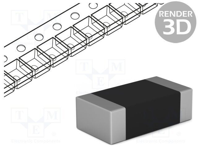
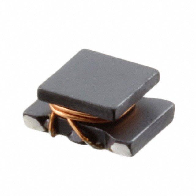
| 产品图片 |
|
| rohs | 符合RoHS无铅 / 符合限制有害物质指令(RoHS)规范要求 |
| 产品系列 | 共模滤波器/扼流器,Murata Electronics DLW31SN222SQ2LEMIFIL®, DLW31S |
| 数据手册 | |
| 产品型号 | DLW31SN222SQ2L |
| 产品 | Common Mode Chokes |
| 产品培训模块 | http://www.digikey.cn/PTM/IndividualPTM.page?site=cn&lang=zhs&ptm=5389 |
| 产品目录绘图 |
|
| 产品目录页面 | |
| 产品种类 | 共模滤波器/扼流器 |
| 其它名称 | 490-1070-1 |
| 包装 | 剪切带 (CT) |
| 单位重量 | 39 mg |
| 商标 | Murata Electronics |
| 外壳宽度 | 1.6 mm |
| 外壳长度 | 3.2 mm |
| 外壳高度 | 1.9 mm |
| 大小/尺寸 | 0.126" 长 x 0.063" 宽(3.20mm x 1.60mm) |
| 安装类型 | 表面贴装 |
| 容差 | 25 % |
| 封装 | Reel |
| 封装/外壳 | 水平式,4 PC 板 |
| 封装/箱体 | 1206 (3216 metric) |
| 尺寸 | 1.6 mm W x 3.2 mm L x 1.9 mm H |
| 屏蔽 | Unshielded |
| 工作温度 | -40°C ~ 85°C |
| 工作温度范围 | - 40 C to + 125 C |
| 工厂包装数量 | 2000 |
| 最大直流电流 | 200 mA |
| 最大直流电阻 | 1.2 Ohms |
| 标准包装 | 1 |
| 测试频率 | 100 MHz |
| 滤波器类型 | 数据,信号线 |
| 电感 | - |
| 电流 | 200mA |
| 端接类型 | SMD/SMT |
| 类型 | Wirewound |
| 系列 | DLW31S |
| 线路数 | 2 |
| 阻抗 | 2.2 kOhms |
| 零件号别名 | PLW3216S222SQ2 |
| 高度(最大值) | 0.083"(2.10mm) |

.jpg)


- 商务部:美国ITC正式对集成电路等产品启动337调查
- 曝三星4nm工艺存在良率问题 高通将骁龙8 Gen1或转产台积电
- 太阳诱电将投资9.5亿元在常州建新厂生产MLCC 预计2023年完工
- 英特尔发布欧洲新工厂建设计划 深化IDM 2.0 战略
- 台积电先进制程称霸业界 有大客户加持明年业绩稳了
- 达到5530亿美元!SIA预计今年全球半导体销售额将创下新高
- 英特尔拟将自动驾驶子公司Mobileye上市 估值或超500亿美元
- 三星加码芯片和SET,合并消费电子和移动部门,撤换高东真等 CEO
- 三星电子宣布重大人事变动 还合并消费电子和移动部门
- 海关总署:前11个月进口集成电路产品价值2.52万亿元 增长14.8%

PDF Datasheet 数据手册内容提取
Reference Only Spec No. JEFL243C-0002U-01 P 1/9 Wire Wound Chip Common Mode Choke Coil DLW31SN□□□SQ2□ Reference Specification 1. Scope This reference specification applies to Chip Common Mode Choke Coil DLW31SN Series. 2. Part Numbering (ex.) DL W 31 S N 222 S Q 2 L (1) (2) (3) (4) (5) (6) (7) (8) (9) (10) (1) Chip Common Mode Choke Coil (6) Impedance (Typ. at 100MHz) (2) Structure (W : Winding Type) (7) Circuit (3) Dimension (L×W) (8) Features (4) Type (9) Number of Line (5) Category (10) Packaging Code L : Taping / B : Bulk 3. Rating Customer Murata Common Mode Impedance Rated Withstanding Rated DC Insulation Part Number Part Number (at 100MHz, Under Voltage Voltage Current Resistance Resistance Standard Testing Condition) V(DC) V(DC) (mA) (Ω max.) (MΩ min.) (Ω ± 25%) DLW31SN222SQ2L 2200 200 1.2 DLW31SN222SQ2B DLW31SN102SQ2L 1000 230 1.0 DLW31SN102SQ2B DLW31SN601SQ2L 600 260 0.8 DLW31SN601SQ2B 50 125 10 DLW31SN261SQ2L 260 310 0.5 DLW31SN261SQ2B DLW31SN161SQ2L 160 340 0.4 DLW31SN161SQ2B DLW31SN900SQ2L 90 370 0.3 DLW31SN900SQ2B Operating Temperature : -40 to +85°C Storage Temperature : -40 to +85°C 4. Standard Testing Condition <Unless otherwise specified> <In case of doubt> Temperature : Ordinary Temperature 15 to 35°C Temperature : 20 ± 2°C Humidity : Ordinary Humidity 25 to 85%(RH) Humidity : 60 to 70%(RH) Atmospheric Pressure : 86 to106kPa 5. Style and Dimensions ■ Equivalent Circuits ) ±0.2 (0.25 (1) (2) 9 1. (4) (3) (0.6) (0.6) No polarity 1.6±0.2 3.2±0.2 ■ Unit Mass (Typical value) 0.039g (1) (2) Electrode (): Referencevalue (4) (3) (inmm) 6. Marking No Marking. MURATA MFG.CO.,LTD
Reference Only Spec No. JEFL243C-0002U-01 P 2/9 7. Electrical Performance No. Item Specification Test Method 7.1 Common Mode Meet item 3. Measuring Equipment : KEYSIGHT 4291A or the Impedance (Zc) equivalent Measuring Frequency :100±1MHz(ref.item 10,11) 7.2 Withstanding Products shall not be Test Voltage : 2.5 times for Rated Voltage Voltage damaged. Time : 1 to 5 seconds Charge Current : 1 mA max. (ref.item 10) 7.3 DC Resistance Meet item 3. Measuring current : 100mA max. (ref.item 10) (Rdc) (In case of doubt in the above mentioned standard condition, measure by 4 terminal method.) 7.4 Insulation Measuring voltage : Rated Voltage Resistance (I.R.) Measuring time : 1 minute max. (ref.item 10) 8. Mechanical Performance No. Item Specification Test Method 8.1 Appearance and Meet item 5. Visual Inspection and measured with Dimensions Slide Calipers. 8.2 Bonding No evidence of coming off It shall be soldered on the substrate. Strength substrate. Applying Force(F) : 9.8N Products shall not be mechanical Applying Time : 5±1 seconds damaged. Pressure Substrate Product Testboardfixture 8.3 Bending Meet Table 1. It shall be soldered on the Glass-epoxy substrate Strength Deflection : 2mm (t=1.0mm) Table 1 Keeping time : 30 seconds Speed of Applying Force : 0.5mm/s Appearance No damaged Pressurejig Common Mode R230 F Impedance within ±20% Change Deflection I.R. 10MΩ min. 45 45 Product 8.4 Drop Withstanding It shall be dropped on concrete or steel board. No damaged Voltage Method : free fall Height : 75 cm The Number of Times : 3 times 8.5 Vibration It shall be soldered on the substrate. Oscillation Frequency : 10 to 55 to 10Hz for 1 minute Total Amplitude : 1.5mm Testing Time : A period of 2 hours in each of 3 mutually perpendicular directions. (Total 6 hours) 8.6 Solderability The electrodes shall be at least Flux : Ethanol solution of rosin,25(wt)% includes 90% covered with new solder activator equivalent to 0.06 to 0.10(wt)% chlorine coating. Pre-Heating : 80 to 120°C 1minute Solder : Sn-3.0Ag-0.5Cu Solder Temperature : 245±3°C Immersion Time : 4±1 s Immersion and emersion rates : 25mm / s Stainlesstweezers Pleaseholdproduct exceptthesepart. 8.7 Resistance to Meet Table 1. Flux : Ethanol solution of rosin,25(wt)% includes Soldering Heat activator equipment to 0.06 to 0.10(wt)% chlorine Pre-Heating : 80 to 120°C ,1minute Solder : Sn-3.0Ag-0.5Cu Solder Temperature : 260±5°C Immersion Time : 5±0.5 seconds Immersion and emersion rates : 25mm / s Then measured after exposure in the room condition for 4 to 48 hours. MURATA MFG.CO.,LTD
Reference Only Spec No. JEFL243C-0002U-01 P 3/9 9. Environmental Performance(Products shall be soldered on the substrate.) No. Item Specification Test Method 9.1 Temperature Meet Table 1. 1 Cycle Cycle Step 1 -40°C(+0°C,-3°C) / 30±3 min Step 2 Ordinary Temp. / 10 to 15 minutes Step 3 +85°C(+3°C,-0°C) / 30±3 min Step 4 Ordinary Temp. / 10 to 15 minutes Total of 10 cycles Then measured after exposure in the room condition for 4 to 48 hours 9.2 Humidity Temperature : 40±2°C Humidity : 90~95%(RH) Time : 1000(+48 hours,-0 hours) Then measured after exposure in the room condition for 4 to 48 hours. 9.3 Heat life Temperature : 85±2°C Applying Voltage : 2times for Rated Voltage Time : 1000(+48 hours,-0 hours) Then measured after exposure in the room condition for 4 to 48 hours. 9.4 Cold Resistance Temperature : -40± 2°C Time : 1000(+48 hours,-0 hours) Then measured after exposure in the room condition for 4 to 48 hours. 10. Terminal to be Tested. When measuring and supplying the voltage,the following terminal is applied. No. Item Terminal to be Tested 10.1 Common Mode Impedance (Measurement Terminal) Terminal Terminal 10.2 Withstanding Voltage Terminal (Measurement Terminal) Terminal 10.3 DC Resistance Terminal Terminal (Measurement Terminal) Terminal Terminal 10.4 Insulation Resistance Terminal (Measurement Terminal) 10.5 Heat Life(Supply Terminal) Terminal 11. Measuring method for common mode impedance. Measured common mode impedance may be included measurement error due to stray capacitance, residual inductance of test fixture. To correct this error, the common mode impedance should be calculate as follows; (1) Measure admittance of the fixture(opened), Go Bo. (2) Measure impedance of the fixture(shorted), Rs Xs. (3) Measure admittance of the specimen, Gm Bm. (4) Calculate corrected impedance Z using the formula below. Z = (Rx2+Xx2) 1/2 Where Gm-GO Rx = - Rs (Gm-Go)2 + (Bm-Bo)2 -(Bm- Bo) Xx = - Xs (Gm-Go) 2 + (Bm-Bo)2 12. P.C.B., Flux, Solder and Soldering condition Test shall be done using P.C.B., Flux, Solder and Soldering condition which are specified in item 16 except the case of being specified special condition. MURATA MFG.CO.,LTD
Reference Only Spec No. JEFL243C-0002U-01 P 4/9 13. Impedance Frequency Characteristics(Typical) 10000 Common Mode DLW31SN222SQ2 DLW31SN102SQ2 DLW31SN601SQ2 1000 DLW31SN261SQ2 DLW31SN161SQ2 ) Ω DLW31SN900SQ2 ( Z | 100 | DLW31SN222SQ2 10 DLW31SN102SQ2 DLW31SN601SQ2 DLW31SN261SQ2 DLW31SN161SQ2 DLW31SN900SQ2 Differential Mode 1 1 10 100 1000 14. Specification of Packaging f (MHz) 14.1 Appearance and Dimensions ( 8mm-wide,Plastic tape) SprocketHole 1 5±0. φ1.5±00.1 4.0±0.1 2.0±0.05 0.3±0.05 1.7 5 8.0±0.2 3.5±0.0 ±0.1 *Dimension of the Cavity is measured 3.6 at the bottom side. 2.1±0.1 2.0±0.1 4.0±0.1 Cavity 14.2 Specification of Taping Directionoffeed (inmm) (1)Packing quantity(Standard quantity) 2000 pcs. / reel (2)Packing Method Products shall be packaged in each embossed cavity of plastic tape and sealed with cover tape. (3) Spliced point The cover tape have no spliced point. (4) Sprocket Hole The sprocket holes are to the right as the tape is pulled toward the user. (5)Missing components number Missing components number within 0.1% of the number per reel or 1 pc., whichever is greater,and are not continuous.The specified quantity per reel is kept. 14.3 Pull Strength of Plastic Tape Plastic Tape 5N min. Cover Tape 10N min. 14.4 Peeling off force of Cover Tape 165to180degree 0.2 to 0.7N(Minimum value is Typical) F Covertape Speed of Peeling off : 300 mm / min Plastictape 14.5 Dimensions of Leader-tape, Trailer and Reel Trailer Leader 2.0±0.5 160min. Label 190min. 210min. Emptytape Toptape φ13.0±0.2 φ60±10 φ21.0±0.8 Directionoffeed 9±1 0 13±1.4 (in:mm) φ180±0 3 MURATA MFG.CO.,LTD
Reference Only Spec No. JEFL243C-0002U-01 P 5/9 14.6 Marking for reel Customer part number, MURATA part number, Inspection number(∗1), RoHS Marking(∗2), Quantity, etc ∗1) « Expression of Inspection No. » □□ OOOO ××× (1) (2) (3) (1) Factory Code (2) Date First digit : Year / Last digit of year Second digit : Month / Jan. to Sep. → 1 to 9, Oct. to Dec. → O,N,D Third, Fourth digit : Day (3) Serial No. ∗2) « Expression of RoHS Marking » ROHS – Y (△) (1) (2) (1) RoHS regulation conformity parts. (2) MURATA classification number 14.7 Marking for Outside package Customer name Purchasing Order Number, Customer Part Number, MURATA part number, RoHS Marking(∗2), Quantity, etc 14.8 Specification of Outer Case Outer Case Dimensions Standard Reel Quantity in Outer Case (mm) (Reel) Label W D H H 186 186 93 5 ∗ Above Outer Case size is typical. It depends on a quantity of an order. D △ W 15. ! Caution 15.1 Mounting Direction Mount products in right direction. Wrong direction which is 90°rotated from right direction causes not only open or short circuit but also flames or other serious trouble. Z Z rightdirection wrongdirection 15.2 Limitation of Applications Please contact us before using our products for the applications listed below which require especially high reliability for the prevention of defects which might directly cause damage to the third party's life,body or property. (1) Aircraft equipment (6) Transportation equipment (vehicles, trains, ships, etc.) (2) Aerospace equipment (7) Traffic signal equipment (3) Undersea equipment (8) Disaster prevention / crime prevention equipment (4) Power plant control equipment (9) Data-processing equipment (5) Medical equipment (10) Applications of similar complexity and /or reliability requirements to the applications listed in the above 16. Notice This product is designed for solder mounting. Please consult us in advance for applying other mounting method such as conductive adhesive. 16.1 Flux and Solder Flux Use rosin-based flux,(with converting chlorine content 0.06 to 0.1(wt)%. ), but not highly acidic flux (with Halogen content exceeding 0.2(wt)% conversion to chlorine). Do not use water-soluble flux. Solder Use Sn-3.0Ag-0.5Cu solder 16.2 Assembling <Exclusive use of Reflow soldering> Products can only be soldered with reflow. Flow soldering may cause deterioration in insulation resistance. So,reflow soldering shall be applied for this product. MURATA MFG.CO.,LTD
Reference Only Spec No. JEFL243C-0002U-01 P 6/9 16.3 Claening Conditions Do not clean after soldering. Some cleaning agents may degrade bonding strength,and characteristics of products by detaching. If cleaning,please contact us. 16.4 Resin coating The impedance value may change due to high cure-stress of resin to be used for coating/molding products. An open circuit issue may occur by mechanical stress caused by the resin, amount/cured shape of resin, or operating condition etc. Some resin contains some impurities or chloride possible to generate chlorine by hydrolysis under some operating condition may cause corrosion of wire of coil, leading to open circuit. So, please pay your careful attention when you select resin in case of coating/molding the products with the resin. Prior to use the coating resin, please make sure no reliability issue is observed by evaluating products mounted on your board. 16.5 Attention regarding P.C.B. bending The following shall be considered when designing and laying out P.C.B.'s. (1) P.C.B. shall be designed so that products are not subject to the mechanical stress due to warping the board. [Products direction] a Products shall be location the sideways b Direction (Length : a<b) to the mechanical Stress. 〈Poorexample〉 〈Goodexample〉 (2)Components location on P.C.B. separation. It is effective to implement the following measures, to reduce stress in separating the board. It is best to implement all of the following three measures; however, implement as many measures as possible to reduce stress. Contents of Measures Stress Level (1) Turn the mounting direction of the component parallel to the board separation surface. A > D *1 (2) Add slits in the board separation part. A > B (3) Keep the mounting position of the component away from the board separation surface. A > C C Perforatio n B *1 A > D is valid when stress is added vertically to the perforation as with Hand Separation. D If a Cutting Disc is used, stress will be diagonal to the PCB, A therefore A > D is invalid. Slit (3) Mounting Components Near Screw Holes When a component is mounted near a screw hole, it may be affected by the board deflection that occurs during the tightening of the screw. Mount the component in a position as far away from the screw holes as possible. Screw Hole Recommended MURATA MFG.CO.,LTD
Reference Only Spec No. JEFL243C-0002U-01 P 7/9 16.6 Attention Regarding P.C.B. Design Portionof < The Arrangement of Products > Perforation P.C.B. shall be designed so that products are × far from the portion of perforation. P.C.B. ○ The portion of perforation shall be designed ○ Product as narrow as possible, and shall be designed Portionof × so as not to be applied the stress in the Perforation case of P.C.B. separation. Products shall not be arranged on the line of a series of holes when there are big P.C.B. ○ × holes in P.C.B. (Because the stress concentrate on the Product line of holes.) Hole < Products Placing > Support pins shall be set under P.C.B . Pick-upnozzle to prevent causing a warp to P.C.B. Product during placing the products on the other side of P.C.B. P.C.B. < P.C.B. Separation > Supportpin P.C.B. shall not be separated with hand. P.C.B. shall be separated with the fixture so as not to cause P.C.B. bending. 16.7 Standard Land Dimensions (Reflow) 4 0. 1 ∗ 6 1. ∗2 Resist 1.6 Copperfoilpattern 3.7 NoPattern (inmm) ∗1 If the pattern is made with wider than 1.6mm. It will result to let component turn around, because melting speed is different. In the worst case, short circuit between lines may be occured. ∗2 If the pattern is made with wider than 1.6mm, the strength of bending will be reduced. ∗3 Do not use gilded pattern. A copper wire may cause open by dissolution of metallization. 16.8 Standard Soldering Condition 1.Reflow Soldering (1) Standard printing pattern of solder paste • Standard thickness of the solder paste should be 100 to 150 µm. 4 6 • Use the solder paste printing pattern of the right pattern. 0. 1. • For the resist and copper foil pattern, use standard land dimensions. • Use the Solder Sn-3.0Ag-0.5Cu for pattern printing. 1.6 • Spread of soldering paste between lines may cause (inmm) 3.7 short circuit of lines. (2) Soldering Temperature Temperature difference between soldering and surface of components must be within 150°C, in preheating. When components are immersed in liquid after soldering, temperature difference should be within 100°C. If preheating is not enough, components may be cracked and cause deterioration in insulation resistance. MURATA MFG.CO.,LTD
Reference Only Spec No. JEFL243C-0002U-01 P 8/9 (3) Soldering Condition Standard soldering profile and the limit soldering profile is as follows. The excessive limit soldering conditions may cause leaching of the electrode and / or resulting in the deterioration of product quality. Temp. 260℃/10s (℃) 245±3℃ 230℃ 220℃ Limit Profile 180 150 Standard Profile 30~60s 60s max. 90s±30s Time(s) Standard Profile Limit Profile Pre-heating 150~180°C 、90s±30s Heating above 220°C、30s~60s above 230°C、60s max. Peak temperature 245±3°C 260°C、10s Cycle of reflow 2 times 2 times 2. Reworking with Soldering iron The following conditions must be strictly followed when using a soldering iron after being mounted by reflow soldering. · Pre-heating: 150°C, 1 min · Soldering iron output: 30W max. · Tip temperature: 350°C max. · Tip diameter:φ3mm max. · Soldering time : 3(+1,-0) seconds. · Times : 2times max. Notes : Do not touch the products directly with the soldering iron. 3. Solder Volume Solder shall be used not to be exceeded the upper limits as shown below. Upperlimit Recommendable t T 1/3T≦t≦T(T:Thicknessofelectrode) Accordingly increasing the solder volume, the mechanical stress to Chip is also increased. Exceeding solder volume may cause the failure of mechanical or electrical performance. 16.9 Caution for use ・When you hold products with a tweezer, please hold tweezer like a figure of the right side, and sharp material, such as a pair of tweezers, shall not be touched to the winding portion to prevent the breaking of wire. ・Mechanical shock should not be applied to the products mounted on the board to prevent the breaking of the core. MURATA MFG.CO.,LTD
Reference Only Spec No. JEFL243C-0002U-01 P 9/9 16.10 Handling of a substrate After mounting products on a substrate, do not apply any stress to the product caused by bending or twisting to the substrate when cropping the substrate, inserting and removing a connector from the substrate or tightening screw to the substrate. Excessive mechanical stress may cause cracking in the product. Bending Twisting 16.11 Brushing of neighborhood of products When you clean the neighborhood of products such as connector pins, bristles of cleaning brush shall not be touched to the winding portion to prevent the breaking of wire. 16.12 Operating Environment Do not use this product under the following environmental conditions, on deterioration of the performance, such as insulation resistance may result from the use. (1) in corrosive gases (acidic gases, alkaline gases, chlorine, sulfur gases, organic gases and etc.) (2) in the atmosphere where liquid such as organic solvent, may splash on the products. 16.13 Storage Condition (1) Storage period Use the products within 12 months after delivered. Solderability should be checked if this period is exceeded. (2) Storage environment conditions ·Products should be stored in the warehouse on the following conditions. Temperature : .-10 ~ +40°C Humidity : 15 to 85% relative humidity No rapid change on temperature and humidity. · Products should not be stored in corrosive gases, such as sulfureous, acid gases, alkaline gases, to prevent the following deterioration. Poor solderability due to the oxidized electrode. · Products should be stored on the palette for the prevention of the influence from humidity,dust and so on. · Products should be stored in the warehouse without heat shock, vibration, direct sunlight and so on. · Products shoud not be stored under the air tights packaged condition. (3) Delivery Care should be taken when transporting or handling product to avoid excessive vibration or mechanical shock. △ 17. ! Note (1)Please make sure that your product has been evaluated in view of your specifications with our product being mounted to your product. (2)You are requested not to use our product deviating from the reference specifications. (3)The contents of this reference specification are subject to change without advance notice. Please approve our product specifications or transact the approval sheet for product specifications before ordering. MURATA MFG.CO.,LTD