ICGOO在线商城 > 开发板,套件,编程器 > 评估板 - 嵌入式 - 复杂逻辑器件(FPGA,CPLD) > DK-SI-4SGX230N
 Datasheet下载
- 型号: DK-SI-4SGX230N
- 制造商: altera
- 库位|库存: xxxx|xxxx
- 要求:
| 数量阶梯 | 香港交货 | 国内含税 |
| +xxxx | $xxxx | ¥xxxx |
查看当月历史价格
查看今年历史价格
DK-SI-4SGX230N产品简介:
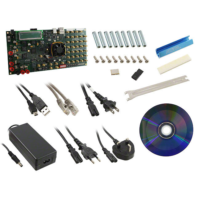
ICGOO电子元器件商城为您提供DK-SI-4SGX230N由altera设计生产,在icgoo商城现货销售,并且可以通过原厂、代理商等渠道进行代购。 DK-SI-4SGX230N价格参考。alteraDK-SI-4SGX230N封装/规格:评估板 - 嵌入式 - 复杂逻辑器件(FPGA,CPLD), EP4SGX230 Stratix® IV GX FPGA Evaluation Board。您可以下载DK-SI-4SGX230N参考资料、Datasheet数据手册功能说明书,资料中有DK-SI-4SGX230N 详细功能的应用电路图电压和使用方法及教程。
Intel 品牌的 DK-SI-4SGX230N 评估板,属于嵌入式复杂逻辑器件(FPGA)类别,主要应用于以下场景:

 1. 工业自动化与控制
   - 实时数据处理:用于工业现场的传感器数据采集、信号处理和实时控制。
   - 运动控制:支持复杂的电机驱动和多轴协调控制,适用于机器人、数控机床等设备。
   - 协议转换:实现不同工业通信协议之间的桥接,如EtherCAT、Profinet、Modbus等。

 2. 通信与网络
   - 信号处理:在通信基站或网络设备中进行高速信号调制解调、编码解码。
   - 数据包处理:用于网络流量分析、路由选择和数据包过滤。
   - 5G基础设施:支持5G NR波形生成、信道编码和大规模MIMO算法。

 3. 图像处理与计算机视觉
   - 视频流处理:对高清或超高清视频流进行实时压缩、解压和格式转换。
   - 边缘计算:在嵌入式系统中实现目标检测、人脸识别等AI推理任务。
   - 医疗成像:用于超声波、CT扫描等医学影像设备的数据处理和图像重建。

 4. 汽车电子
   - ADAS(高级驾驶辅助系统):实现车道偏离预警、自动紧急制动等功能。
   - 自动驾驶:处理来自雷达、激光雷达和摄像头的海量数据,进行环境感知和决策。
   - 车载娱乐系统:支持多媒体解码、显示驱动和音频处理。

 5. 消费电子
   - 智能家居:用于智能家电的嵌入式控制和语音识别。
   - 游戏设备:提供高性能图形渲染和物理仿真功能。
   - 可穿戴设备:实现低功耗传感器融合和健康数据监测。

 6. 科研与教育
   - 原型开发:为研究人员和学生提供一个灵活的硬件平台,用于验证算法和设计。
   - 教学实验:帮助学生学习FPGA编程、数字电路设计和嵌入式系统开发。

DK-SI-4SGX230N 评估板基于 Intel Stratix IV FPGA 系列,具有强大的逻辑资源、丰富的I/O接口和高速串行收发器,适合需要高计算性能和灵活性的应用场景。通过该板,开发者可以快速验证设计、优化性能并加速产品上市时间。
| 参数 | 数值 |
| 产品目录 | 编程器,开发系统嵌入式解决方案 |
| 描述 | KIT DEV STRATIX IV 4SGX230N/C2可编程逻辑 IC 开发工具 FPGA Development Kit For EP4SGX230 |
| 产品分类 | 评估板 - 嵌入式 - 复杂逻辑器件 (FPGA, CPLD)工程工具 |
| 品牌 | Altera Corporation |
| 产品手册 | |
| 产品图片 |
|
| rohs | 符合RoHS无铅 / 符合限制有害物质指令(RoHS)规范要求 |
| 产品系列 | 嵌入式开发工具,可编程逻辑 IC 开发工具,Altera Corporation DK-SI-4SGX230NStratix® IV GX |
| 数据手册 | 点击此处下载产品Datasheet点击此处下载产品Datasheet点击此处下载产品Datasheet点击此处下载产品Datasheet |
| 产品型号 | DK-SI-4SGX230N |
| 产品 | Development Kits |
| 产品培训模块 | http://www.digikey.cn/PTM/IndividualPTM.page?site=cn&lang=zhs&ptm=25450 |
| 产品目录页面 | |
| 产品种类 | 可编程逻辑 IC 开发工具 |
| 其它名称 | 544-2592 |
| 兼容软件 | Quartus II |
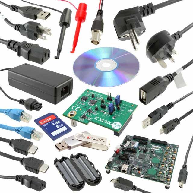
| 内容 | 板,线缆,电源 |
| 商标 | Altera Corporation |
| 商标名 | Stratix |
| 工作电源电压 | 16 V |
| 工具用于评估 | EP4SGX230KF40C2N |
| 接口类型 | Ethernet, JTAG, USB |
| 描述/功能 | Stratix IV GX development kit |
| 标准包装 | 1 |
| 相关产品 | /product-detail/zh/EP4SGX230KF40C3N/EP4SGX230KF40C3N-ND/2057264/product-detail/zh/EP4SGX230KF40C3/EP4SGX230KF40C3-ND/2057263/product-detail/zh/EP4SGX230HF35C3N/EP4SGX230HF35C3N-ND/2057262/product-detail/zh/EP4SGX230HF35C3/EP4SGX230HF35C3-ND/2057261/product-detail/zh/EP4SGX230FF35C3NES/EP4SGX230FF35C3NES-ND/2057260/product-detail/zh/EP4SGX230FF35C3ES/EP4SGX230FF35C3ES-ND/2057259/product-detail/zh/EP4SGX230DF29C3NES/EP4SGX230DF29C3NES-ND/2057258/product-detail/zh/EP4SGX230DF29C3ES/EP4SGX230DF29C3ES-ND/2057257 |
| 类型 | FPGA |
| 系列 | Stratix IV |
| 配套使用产品/相关产品 | EP4SGX230 |


- 商务部:美国ITC正式对集成电路等产品启动337调查
- 曝三星4nm工艺存在良率问题 高通将骁龙8 Gen1或转产台积电
- 太阳诱电将投资9.5亿元在常州建新厂生产MLCC 预计2023年完工
- 英特尔发布欧洲新工厂建设计划 深化IDM 2.0 战略
- 台积电先进制程称霸业界 有大客户加持明年业绩稳了
- 达到5530亿美元!SIA预计今年全球半导体销售额将创下新高
- 英特尔拟将自动驾驶子公司Mobileye上市 估值或超500亿美元
- 三星加码芯片和SET,合并消费电子和移动部门,撤换高东真等 CEO
- 三星电子宣布重大人事变动 还合并消费电子和移动部门
- 海关总署:前11个月进口集成电路产品价值2.52万亿元 增长14.8%


PDF Datasheet 数据手册内容提取
Transceiver Signal Integrity Development Kit, Stratix IV GX Edition User Guide Transceiver Signal Integrity Development Kit, Stratix IV GX Edition User Guide 101 Innovation Drive San Jose, CA 95134 www.altera.com UG-01057-2.1 Subscribe
© 2011 Altera Corporation. All rights reserved. ALTERA, ARRIA, CYCLONE, HARDCOPY, MAX, MEGACORE, NIOS, QUARTUS and STRATIX words and logos are trademarks of Altera Corporation and registered in the U.S. Patent and Trademark Office and in other countries. All other words and logos identified as trademarks or service marks are the property of their respective holders as described at www.altera.com/common/legal.html. Altera warrants performance of its ISO semiconductor products to current specifications in accordance with Altera's standard warranty, but reserves the right to make changes to any products and 9001:2008 services at any time without notice. Altera assumes no responsibility or liability arising out of the application or use of any information, product, or service Registered described herein except as expressly agreed to in writing by Altera. Altera customers are advised to obtain the latest version of device specifications before relying on any published information and before placing orders for products or services. December 2011 Altera Corporation Transceiver Signal Integrity Development Kit, Stratix IV GX Edition User Guide
Contents Chapter1. About This Kit Kit Features . . . . . . . . . . . . . . . . . . . . . . . . . . . . . . . . . . . . . . . . . . . . . . . . . . . . . . . . . . . . . . . . . . . . . . . . . . . . 1–1 Software . . . . . . . . . . . . . . . . . . . . . . . . . . . . . . . . . . . . . . . . . . . . . . . . . . . . . . . . . . . . . . . . . . . . . . . . . . . . . 1–2 Transceiver Signal Integrity Development Kit, Stratix IV GX Edition Installer . . . . . . . . . . . . . . . 1–2 Chapter2. Getting Started Before You Begin . . . . . . . . . . . . . . . . . . . . . . . . . . . . . . . . . . . . . . . . . . . . . . . . . . . . . . . . . . . . . . . . . . . . . . . . 2–1 Check the Kit Contents . . . . . . . . . . . . . . . . . . . . . . . . . . . . . . . . . . . . . . . . . . . . . . . . . . . . . . . . . . . . . . . . 2–1 Inspect the Board . . . . . . . . . . . . . . . . . . . . . . . . . . . . . . . . . . . . . . . . . . . . . . . . . . . . . . . . . . . . . . . . . . . . . 2–1 Hardware Requirements . . . . . . . . . . . . . . . . . . . . . . . . . . . . . . . . . . . . . . . . . . . . . . . . . . . . . . . . . . . . . . . 2–2 Software Requirements . . . . . . . . . . . . . . . . . . . . . . . . . . . . . . . . . . . . . . . . . . . . . . . . . . . . . . . . . . . . . . . . 2–2 Quartus II Programmer System Requirements . . . . . . . . . . . . . . . . . . . . . . . . . . . . . . . . . . . . . . . . . . . . 2–2 References . . . . . . . . . . . . . . . . . . . . . . . . . . . . . . . . . . . . . . . . . . . . . . . . . . . . . . . . . . . . . . . . . . . . . . . . . . . . . . 2–2 Chapter3. Software Installation Installing the Transceiver Signal Integrity Development Kit, StratixIVGX Edition . . . . . . . . . . . . . . . 3–1 Installing the Quartus II Software . . . . . . . . . . . . . . . . . . . . . . . . . . . . . . . . . . . . . . . . . . . . . . . . . . . . . . . . . . 3–2 Installing the USB-Blaster Driver . . . . . . . . . . . . . . . . . . . . . . . . . . . . . . . . . . . . . . . . . . . . . . . . . . . . . . . . . . 3–3 Chapter4. Development Board Setup Powering Up the Board . . . . . . . . . . . . . . . . . . . . . . . . . . . . . . . . . . . . . . . . . . . . . . . . . . . . . . . . . . . . . . . . . . 4–1 Chapter5. Board Update Portal Board Update Portal . . . . . . . . . . . . . . . . . . . . . . . . . . . . . . . . . . . . . . . . . . . . . . . . . . . . . . . . . . . . . . . . . . . . . 5–1 Connecting to the Board Update Portal Web Page . . . . . . . . . . . . . . . . . . . . . . . . . . . . . . . . . . . . . . . . . 5–1 Using the Board Update Portal to Update Designs . . . . . . . . . . . . . . . . . . . . . . . . . . . . . . . . . . . . . . . . . 5–2 Chapter6. Stratix IV GX Transceiver Signal Integrity Demonstration Test Designs . . . . . . . . . . . . . . . . . . . . . . . . . . . . . . . . . . . . . . . . . . . . . . . . . . . . . . . . . . . . . . . . . . . . . . . . . . . . 6–1 Configuring the FPGA Using Quartus II Programmer . . . . . . . . . . . . . . . . . . . . . . . . . . . . . . . . . . . . . . . . 6–1 LCD Information . . . . . . . . . . . . . . . . . . . . . . . . . . . . . . . . . . . . . . . . . . . . . . . . . . . . . . . . . . . . . . . . . . . . . . . . 6–2 Running the Demonstration Application and Test Designs . . . . . . . . . . . . . . . . . . . . . . . . . . . . . . . . . . . . 6–2 Demonstration Application Description . . . . . . . . . . . . . . . . . . . . . . . . . . . . . . . . . . . . . . . . . . . . . . . . . . 6–3 Analog Settings . . . . . . . . . . . . . . . . . . . . . . . . . . . . . . . . . . . . . . . . . . . . . . . . . . . . . . . . . . . . . . . . . . . . 6–3 Resets . . . . . . . . . . . . . . . . . . . . . . . . . . . . . . . . . . . . . . . . . . . . . . . . . . . . . . . . . . . . . . . . . . . . . . . . . . . . . 6–4 Help . . . . . . . . . . . . . . . . . . . . . . . . . . . . . . . . . . . . . . . . . . . . . . . . . . . . . . . . . . . . . . . . . . . . . . . . . . . . . . 6–4 Power Down . . . . . . . . . . . . . . . . . . . . . . . . . . . . . . . . . . . . . . . . . . . . . . . . . . . . . . . . . . . . . . . . . . . . . . . 6–4 Serial Loopback . . . . . . . . . . . . . . . . . . . . . . . . . . . . . . . . . . . . . . . . . . . . . . . . . . . . . . . . . . . . . . . . . . . . 6–4 Autolink Setup . . . . . . . . . . . . . . . . . . . . . . . . . . . . . . . . . . . . . . . . . . . . . . . . . . . . . . . . . . . . . . . . . . . . . 6–5 Autolink Start and Stop . . . . . . . . . . . . . . . . . . . . . . . . . . . . . . . . . . . . . . . . . . . . . . . . . . . . . . . . . . . . . 6–5 Data Patterns . . . . . . . . . . . . . . . . . . . . . . . . . . . . . . . . . . . . . . . . . . . . . . . . . . . . . . . . . . . . . . . . . . . . . . 6–6 Link Statistics Tab . . . . . . . . . . . . . . . . . . . . . . . . . . . . . . . . . . . . . . . . . . . . . . . . . . . . . . . . . . . . . . . . . . 6–6 PCI Express Tab . . . . . . . . . . . . . . . . . . . . . . . . . . . . . . . . . . . . . . . . . . . . . . . . . . . . . . . . . . . . . . . . . . . . 6–7 Power and Temperature Tab . . . . . . . . . . . . . . . . . . . . . . . . . . . . . . . . . . . . . . . . . . . . . . . . . . . . . . . . . 6–7 Channel Reconfig Tab . . . . . . . . . . . . . . . . . . . . . . . . . . . . . . . . . . . . . . . . . . . . . . . . . . . . . . . . . . . . . . . 6–7 EyeQ Tab . . . . . . . . . . . . . . . . . . . . . . . . . . . . . . . . . . . . . . . . . . . . . . . . . . . . . . . . . . . . . . . . . . . . . . . . . . 6–8 AppendixA. Programming the Flash Device December 2011 Altera Corporation Transceiver Signal Integrity Development Kit, Stratix IV GX Edition User Guide
iv ContentsContents Board Update Portal CFI Flash Memory Map . . . . . . . . . . . . . . . . . . . . . . . . . . . . . . . . . . . . . . . . . . . . . . A–1 Parallel Flash Loader . . . . . . . . . . . . . . . . . . . . . . . . . . . . . . . . . . . . . . . . . . . . . . . . . . . . . . . . . . . . . . . . . . . A–2 Custom User Design . . . . . . . . . . . . . . . . . . . . . . . . . . . . . . . . . . . . . . . . . . . . . . . . . . . . . . . . . . . . . . . . . A–2 Creating Flash Files Using the Nios II EDS . . . . . . . . . . . . . . . . . . . . . . . . . . . . . . . . . . . . . . . . . . . . . . . . . A–2 Nios II EDS Flash Programming Instructions . . . . . . . . . . . . . . . . . . . . . . . . . . . . . . . . . . . . . . . . . . . . . . . A–3 Restoring the Factory Design to the Flash Device . . . . . . . . . . . . . . . . . . . . . . . . . . . . . . . . . . . . . . . . . . . A–4 Nios II EDS Recovery Instructions . . . . . . . . . . . . . . . . . . . . . . . . . . . . . . . . . . . . . . . . . . . . . . . . . . . . . . A–4 Additional Information Revision History . . . . . . . . . . . . . . . . . . . . . . . . . . . . . . . . . . . . . . . . . . . . . . . . . . . . . . . . . . . . . . . . . . . . . Info–1 Typographic Conventions . . . . . . . . . . . . . . . . . . . . . . . . . . . . . . . . . . . . . . . . . . . . . . . . . . . . . . . . . . . . . Info–2 Transceiver Signal Integrity Development Kit, December 2011 Altera Corporation Stratix IV GX Edition User Guide
1. About This Kit The Transceiver Signal Integrity Development Kit, Stratix® IV GX Edition provides everything you need for the signal integrity evaluation and interoperability of StratixIV GX transceivers on the Altera® Stratix IV GX EP4SGX230 device. The kit includes a full-featured FPGA development board, hardware and software evaluation tools, documentation, and accessories needed to begin development. With this signal integrity development kit, you can do the following: ■ Evaluate transceiver performance at data rate ranging from 600 Mbps to 8.5 Gbps. ■ Generate and check pseudo-random binary sequence (PRBS) patterns through an easy-to-use demonstration application. ■ Understand the effects of changing differential output voltage (V ), preemphasis, OD and equalization settings. ■ Perform jitter analysis. ■ Verify physical medium attachment (PMA) compliance to PCI Express (Gen 1 and Gen 2), Serial RapidIO®, gigabit Ethernet, 10 gigabit Ethernet XAUI, CEI-6G, high definition serial digital interface (HD-SDI), Fibre Channel 1G/4G/8G, and other major standards. m For a demostration of this development kit, refer to the video Analyze FPGA Transceiver Interoperability & Signal Integrity on the Webcasts and Videos page of the Altera website. Kit Features This section briefly describes the following Stratix IV GX transceiver signal integrity development kit features: ■ Stratix IV GX EP4SGX230 Signal Integrity Transceiver Development Board—a development platform that allows you to develop and prototype hardware designs running on the StratixIVGX FPGA (ordering code: DK-SI-4SGX230N). f For detailed information about board components and interfaces, refer to the Transceiver Signal Integrity Development Kit, Stratix IV GX Edition Reference Manual. December 2011 Altera Corporation Transceiver Signal Integrity Development Kit, Stratix IV GX Edition User Guide
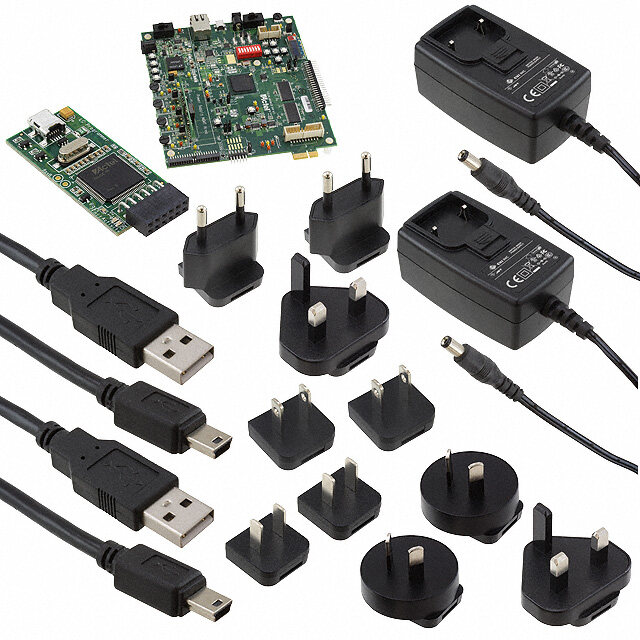
1–2 Chapter 1: About This Kit Kit Features ■ Transceiver Signal Integrity Development Kit, Stratix IV GX Edition includes the following: ■ Schematic and board design files ■ Design examples for the Board Update Portal Embedded Nios® II webserver and the Golden Top Level Project ■ Device data sheets ■ Stratix IV GX Transceiver Signal Integrity Demonstration software ■ Quartus II Stand-Alone Programmer software ■ Stratix IV GX signal integrity development kit application and device driver ■ Complete documentation: ■ Transceiver Signal Integrity Development Kit, Stratix IV GX Edition User Guide (this document)—Describes how to use the kit. ■ Transceiver Signal Integrity Development Kit, Stratix IV GX Edition Reference Manual—Provides specific information about the board components and interfaces, steps for using the board, and pin-outs and signal specifications. ■ Readme.txt—Contains special instructions and refers to the kit documentation. ■ Power Supply and Cable—The following items are included in the development kit: ■ USB cable ■ Ethernet CAT-5/RJ-45 cable ■ Power supply and AC adapters for North America, Japan, Europe, and the United Kingdom Software The software for this kit, described in the following sections, is available on the Altera website for immediate downloading. You can also request to have Altera mail the software to you on DVDs. Transceiver Signal Integrity Development Kit, Stratix IV GX Edition Installer The license-free Transceiver Signal Integrity Development Kit, Stratix IV GX Edition installer includes all the documentation and design examples for the kit. Download the kit installer from the Transceiver Signal Integrity Development Kit, Stratix IV GX Edition page of the Altera website. Alternatively, you can request a Development Kit DVD from the Altera Kit Installations DVD Request Form page of the Altera website. Transceiver Signal Integrity Development Kit, December 2011 Altera Corporation Stratix IV GX Edition User Guide
2. Getting Started This user guide familiarizes you with the contents of the kit and guides you through the Stratix IV GX transceiver signal integrity board setup. Using this user guide, you can do the following: ■ Inspect the contents of the kit ■ Install the Transceiver Signal Integrity Development Kit, Stratix IV GX Edition software ■ Set up, power up, and verify correct operation of the signal integrity board ■ Configure the StratixIV GX FPGA ■ Run the signal integrity software and use the test designs f For complete information about the signal integrity board, refer to the Transceiver Signal Integrity Development Kit, Stratix IV GX Edition Reference Manual. Before You Begin Before using the kit or installing the software, check the kit contents and inspect the board to verify that you received all of the items listed in this section. If any of the items are missing, contact Altera before you proceed. Check the Kit Contents Refer to “Kit Features” on page1–1 for the contents of your kit. f To ensure that you have the most up-to-date information about this product, refer to the Stratix IV GX FPGA Development Kit page. Inspect the Board To inspect the board, perform the following steps: 1. Place the board on an anti-static surface and inspect it to ensure that it has not been damaged during shipment. c Without proper anti-static handling, the Stratix IV GX transceiver signal integrity board can be damaged. 2. Verify that all components are on the board and appear intact. 1 In typical applications with the Stratix IV GX transceiver signal integrity board, a heat sink is not necessary. However, under extreme conditions the board may require additional cooling to stay within operating temperature guidelines. You may wish to perform power consumption and thermal modeling to determine whether your application requires additional cooling. December 2011 Altera Corporation Transceiver Signal Integrity Development Kit, Stratix IV GX Edition User Guide
2–2 Chapter 2: Getting Started References f For more information about power consumption and thermal modeling, refer to AN358: Thermal Management for FPGAs. Hardware Requirements The kit provides all the hardware you need to use the board. Software Requirements The kit requires the following software: ■ Quartus II Subscription Edition software (to run the demonstration GUI) 1 Certain DLLs that are required for the demonstration application (stratixIVGX_si_demo.exe) to function properly are not included with the kit installation software. These needed DLLs are installed with the Quartus II Subscription Edition software, versions 9.1, 9.1sp1, or 9.1sp2. Make sure you successfully display the main Quartus II GUI at least once. If you don’t want to purchase a license, you can uninstall the Quartus II software; the demonstration application will continue to function properly. Refer to “Installing the Quartus II Software” on page3–2. ■ Quartus II Programmer ■ Windows XP operating system or later Quartus II Programmer System Requirements The Quartus II Programmer has some minimum system requirements. f For Quartus II Programmer system requirements, refer to the Altera website at: www.altera.com/products/software/products/quartus2web/sof- quarwebmain.html. References For other related information, refer to the following websites: ■ For additional daughter cards available for purchase: www.altera.com/products/devkits/kit-daughter_boards.jsp ■ For the StratixIV device documentation: www.altera.com/literature/lit-stratix-iv.jsp ■ For the eStore if you want to purchase devices: www.altera.com/buy/devices/buy-devices.html ■ For StratixIV GX OrCAD symbols: www.altera.com/support/software/download/pcb/pcb-pcb_index.html ■ For NiosII 32-bit embedded processor solutions: www.altera.com/technology/embedded/emb-index.html Transceiver Signal Integrity Development Kit, December 2011 Altera Corporation Stratix IV GX Edition User Guide
Chapter 2: Getting Started 2–3 References ■ For NiosII 32-bit embedded processor solutions: www.altera.com/technology/embedded/emb-index.html December 2011 Altera Corporation Transceiver Signal Integrity Development Kit, Stratix IV GX Edition User Guide
2–4 Chapter 2: Getting Started References Transceiver Signal Integrity Development Kit, December 2011 Altera Corporation Stratix IV GX Edition User Guide
3. Software Installation The instructions in this chapter explain how to install the following software: ■ Transceiver Signal Integrity Development Kit, Stratix IV GX Edition software. ■ Quartus II software—Certain DLLs that are required for the demonstration application (stratixIVGX_si_demo.exe) to function properly are not included with the kit installation software. These needed DLLs are installed with the Quartus II Subscription Edition software, versions 9.1, 9.1sp1, or 9.1sp2. Make sure you can successfully display the main Quartus II GUI at least once. If you don’t want to purchase a license, you can uninstall the Quartus II software; the demonstration application will continue to function properly. Refer to “Installing the Quartus II Software” on page3–2. ■ USB-Blaster driver. Before starting the installation, verify that you have complied with the conditions described in “Software Requirements” on page2–2. Installing the Transceiver Signal Integrity Development Kit, Stratix IV GX Edition To install the Transceiver Signal Integrity Development Kit, Stratix IV GX Edition, perform the following steps: 1. Run the kit installer you acquired in “Software” on page1–2. 2. Follow the on-screen instructions to complete the installation process. Be sure that the installation directory you choose is in the same relative location to the QuartusII software installation. December 2011 Altera Corporation Transceiver Signal Integrity Development Kit, Stratix IV GX Edition User Guide
3–2 Chapter 3: Software Installation Installing the Quartus II Software The installation program creates the Transceiver Signal Integrity Development Kit, Stratix IV GX Edition directory structure shown in Figure3–1. Figure3–1. Stratix IV GX Transceiver Signal Integrity Kit Installed Directory Structure <install dir> The default Windows installation directory is C:\altera\<version>\. kits stratixIVGX_4sgx230_si board_design_files demos documents examples factory_recovery Note to Figure3–1: (1) Early-release (engineering silicon) versions might have slightly different directory names. Table3–1 lists the file directory names and a description of their contents. Table3–1. Installed Directory Contents Directory Name Description of Contents Contains schematic, layout, assembly, and bill of material board design files. Use these files as a board_design_files starting point for a new prototype board design. demos Contains demonstration applications that may change from release to release. documents Contains the development kit documentation. examples Contains the sample design files for the StratixIV GX transceiver signal integrity development kit. Contains the original data programmed onto the board before shipment. Use this data to put the factory_recovery board into the original condition. Installing the Quartus II Software The QuartusII software and the Nios II Embedded Design Suite (EDS) are the primary FPGA development tools used to create the reference designs in this development kit. To run the demonstration application or to create new designs, perform the following steps: 1. Go to Altera’s Download Center. 2. Follow the online instructions to complete the installation process to install the Quartus II software. Transceiver Signal Integrity Development Kit, December 2011 Altera Corporation Stratix IV GX Edition User Guide
Chapter 3: Software Installation 3–3 Installing the USB-Blaster Driver 1 Certain DLLs that are required for the demonstration application (stratixIVGX_si_demo.exe) to function properly are not included with the kit installation software. These needed DLLs are installed with the Quartus II Subscription Edition software, versions 9.1, 9.1sp1, or 9.1sp2. Make sure you successfully display the main Quartus II GUI at least once. If you don’t want to purchase a license, you can uninstall the Quartus II software; the demonstration application will continue to function properly. f If you have difficulty installing the Quartus II software, refer to the QuartusII Installation & Licensing for Windows and Linux Workstations. Installing the USB-Blaster Driver The StratixIV GX transceiver signal integrity board includes integrated USB-Blaster circuitry for FPGA programming. However, for the host computer and signal integrity board to communicate, you must install the USB-Blaster driver on the host computer. To download the USB-Blaster driver, go to the Altera support site at www.altera.com/support/software/drivers/dri-index.html. To install it, go to www.altera.com/support/software/drivers/usb-blaster/dri-usb- blaster-xp.html. December 2011 Altera Corporation Transceiver Signal Integrity Development Kit, Stratix IV GX Edition User Guide
3–4 Chapter 3: Software Installation Installing the USB-Blaster Driver Transceiver Signal Integrity Development Kit, December 2011 Altera Corporation Stratix IV GX Edition User Guide
4. Development Board Setup The instructions in this chapter explain how to power up the signal integrity development board. Powering Up the Board To power up the board, perform the following steps: 1. Verify that the MAX/JTAG jumper J26 is OFF, and that the mini-DIP switch SW2 settings located adjacent to jumper J62 match the settings in the following table: Table4–1. Switch Pin SW2.1 SW2.2 SW2.3 SW2.4 Label S0 S1 S2 S3 Position up or 0 down or 1 down or 1 down or 1 1 Maintain these settings as they control the speed of the board oscillator. For more information, refer to the Transceiver Signal Integrity Development Kit, Stratix IV GX Edition Reference Manual. 2. Connect the power cable to the board and plug the other end into a power outlet. 3. Connect the DC adapter (+16V, 3.75A) to the DC power jack (J1). c Use only the supplied 16-V power supply. Power regulation circuitry on the board could be damaged by supplies greater than 16V. 4. Ensure the POWER switch (SW1) is in the ON position. When power is supplied to the board, LED D3 turns on indicating that the board has power. After the board powers up, the on-board flash memory, which ships preprogrammed with the factory design, automatically configures the Stratix IV GX device. The FACTORY LED illuminates, signaling that the Stratix IV GX device is configured with the preprogrammed factory design. December 2011 Altera Corporation Transceiver Signal Integrity Development Kit, Stratix IV GX Edition User Guide
4–2 Chapter 4: Development Board Setup Powering Up the Board Transceiver Signal Integrity Development Kit, December 2011 Altera Corporation Stratix IV GX Edition User Guide
5. Board Update Portal This chapter describes the Board Update Portal which allows you to upload new designs and provides access to useful and relevant information about the kit. Board Update Portal This development kit is shipped with an example design stored in the factory portion of the flash memory on the board. Whenever jumper J62 is set to LOAD FACTORY, the Stratix IV GX FPGA is automatically configured with the Board Update Portal example design. The example design is an embedded web server, which serves the Board Update Portal web page. The web page allows you to upload new FPGA designs to the designated flash memory on your board, and also provides links to useful information, on the Altera website at www.altera.com, including links to kit-specific and design resources. After the Board Update Portal is used to successfully update a design, jumper J62 can be set to LOAD and the design configures upon reset or power up. To do so, set the configuration program select jumper, PGMSEL, (J62) to the position (jump pins 1-2) and power cycle the board. This cycle can be repeated for different designs as long as the factory Board Update Portal is preserved. If the Board Update Portal is corrupted or deleted from the flash memory, refer to “Restoring the Factory Design to the Flash Device” on pageA–4 to restore the board to factory condition. The source for the Board Update Portal design resides in the <install dir\kits\stratixIVGX_4sgx230_si\examples. It consists of a Nios II embedded processor, an Ethernet MAC, and an HTML web server. When the board is connected to the network, the Nios II processor obtains an IP address and allows the browser access to its HTML web page. This section provides instructions on how to connect to the Board Update Portal web page. 1 Before you proceed, ensure that you have the following: ■ A PC with a connection to a working Ethernet port on a DHCP enabled network. ■ A separate working Ethernet port connected to the same network for the board. ■ The Ethernet and power cables that are included in the kit. Connecting to the Board Update Portal Web Page 1. With the board powered down, make sure jumper J62 is in the LOAD FACTORY position (pins 2-3). 2. Attach the Ethernet cable from the board to the LAN. 3. Power up the board. The board connects to the LAN’s gateway router, and obtains an IP address. The LCD on the board displays the IP address. December 2011 Altera Corporation Transceiver Signal Integrity Development Kit, Stratix IV GX Edition User Guide
5–2 Chapter 5: Board Update Portal Board Update Portal 4. Launch a web browser on a PC that is connected to the same network, and enter the IP address from the LCD into the browser address bar. The Board Update Portal web page appears in the browser page. 5. Click Signal Integrity Development Kit to view the latest version of the development kit software. 1 If you download new software, double-click the downloaded .exe file to begin the installation process. 1 Visit the Board Update Portal web page to check for additional new designs and documentation updates. f If the Board Update Portal cannot connect for some reason, then go to www.altera.com/products/devkits/altera/kit-signal_integrity_sivgx.html to ensure that the board has the latest kit software. Using the Board Update Portal to Update Designs The Board Update Portal allows remote update of new FPGA configurations to the flash memory. Perform the following steps to update the memory on your board with a design downloaded from the Altera website. 1. Type the IP address displayed on the LCD into the web browser on the PC or use the browser’s Back button to return to the main Board Update Portal web page. 2. Click the Browse button next to the Hardware File Name field and browse to the new .flash file that was downloaded. If there is a software component to the design, then include it in the same manner in the Software File Name field, otherwise leave the field empty. 3. Click Upload. The progress bar indicates the percent complete. 4. After the upload process is complete, the FPGA can be configured with the new image. To do this, change jumper J62 to LOAD (jump pins 1-2). To enable reconfiguration of the FPGA, power up the board again or press RESET SW8. The design running in flash is the selected .flash file. 1 As long as the factory image is not overwritten, the Board Update Portal can be used to update new images in the same manner. If the factory memory image is overwritten, it can be restored by following the instructions in “Restoring the Factory Design to the Flash Device” on pageA–4. Transceiver Signal Integrity Development Kit, December 2011 Altera Corporation Stratix IV GX Edition User Guide
6. Stratix IV GX Transceiver Signal Integrity Demonstration The kit installs a demonstration application and test designs. The application provides an easy-to-use interface where you can select various transceiver settings and observe the result. Before you run the application and test designs, connect the USB cable to the board and navigate to the Stratix IV GX Transceiver Signal Integrity Demonstration application as explained in “Installing the Transceiver Signal Integrity Development Kit, StratixIVGX Edition” on page3–1. Test Designs Altera provides a set of test designs for the evaluation of the StratixIVGX device transceiver performance and board features. The .sof file names and data rates for each test design are listed in Table6–1. Before you run the application, use the Quartus II Programmer to configure the Stratix IV GX device with one of the .sof files. Table6–1. Data Rates for Test Designs Transceiver Transceiver Transceiver Transceiver Block1 Block1 Block0 Block 2 Channel 1, Channel 3, File Name Channel 0 Channel 7 Clocking scheme Channel 2 Channel 4 Data Rate Data Rate Data Rate Data Rate (Gbps) (Gbps) (Gbps) (Gbps) PCI Express signal_integrity_demo1.sof soc_clk*20 (1) 3.125 soc_clk*20 (1) socket clock (Gen1 or Gen2) signal_integrity_demo2.sof soc_clk*20 (1) soc_clk*20 (1) soc_clk*20 (1) soc_clk*20 (1) socket clock socket clock or Refer to “Channel Reconfig Tab” on page6–7 for the available signal_integrity_demo3.sof external SMA clock transceiver channel data rates and functional modes. (J19 and J20) Note to Table6–1: (1) The clock input is expected from the socketed oscillator (Y3) (soc_clk) on the board. If you are targeting –2 speed grade device on the board, you can use 425 MHz. For –3 speed grade, the maximum data rate limit supported is 6.5 Gbps. Therefore, you must use 312.5 MHz (312.5*20 < 6.5 Gbps) and not the 425-MHz clock crystal. Configuring the FPGA Using Quartus II Programmer It is sometimes necessary to use the Quartus II Programmer to configure the FPGA with specific .sof files, such as the designs in Table6–1. Before configuring the FPGA, ensure that the Quartus II Programmer and the USB-Blaster driver are installed on the host computer and the development board is powered up. To configure the StratixIV GX FPGA, perform the following steps: 1. Start the QuartusII Programmer. 2. Click Add File and select the path to the desired .sof. 3. Turn on the Program/Configure option for the added file. 4. Click Start to download the selected file to the FPGA. The FPGA is configured when the progress bar reaches 100%. December 2011 Altera Corporation Transceiver Signal Integrity Development Kit, Stratix IV GX Edition User Guide
6–2 Chapter 6: Stratix IV GX Transceiver Signal Integrity Demonstration LCD Information 1 To determine if the appropriate test design .sof is programmed, check the LCD for the test design number. Refer to “LCD Information” for more information. LCD Information The LCD shows the following information: ■ The Stratix IV GX device junction temperature in Celsius. ■ The power in watts for the different transceivers (VCCA_L/R, VCCT, VCCR, VCCH_GXB, VCCL_GXB) and core (VCC) voltage supply rails. Turn the rotary switch SW16 to observe the different voltage supply values. To learn more about the switch position for displaying the various supply rail values on the LCD, click the Help button in the demonstration application. ■ The sof/pof number that is programmed is indicated by ‘pof’ followed by the number. The power values shown for the VCCA_L/R and the VCCH_GXB assume that the jumper settings are set to 3.0V and 2.5V, respectively. Click the Help button to see the required jumper settings. Running the Demonstration Application and Test Designs The demonstration application communicates with the set of test designs provided with the kit. You can change the various transceiver parameters that are described in this section. To run the application, make sure that the board is powered up properly and there is a USB cable attached, then go to the <installdir>\kits\stratixIVGX_4sgx230_si\demos\ directory and double-click on stratixIVGX_si_demo.exe file. Ensure that the StratixIV FPGA is programmed with the .sof specified in Table6–1 on page6–1. 1 Certain DLLs are required for the demonstration application (stratixIVGX_si_demo.exe) to function properly that are not included with the kit installation software. These needed DLLs are installed with the Quartus II Subscription Edition software, version 9.1. Once installed, you can immediately uninstall the Quartus II software afterwards if you don’t want to purchase a license. Refer to “Installing the Quartus II Software” on page3–2. To enable the application to communicate with the board, click the Connect button. To close the application, click the Disconnect button (Figure6–1). 1 Because the demonstration application communicates with the board using the same interface as the Quartus II Programmer or SignalTap®II Embedded Logic Analyzer, you can run only one of these applications at a time. 1 The application will not run unless the USB cable is attached, power is applied, and the correct .sof is programmed to the Stratix IV GX FPGA as specified in Table6–1 on page6–1. Transceiver Signal Integrity Development Kit, December 2011 Altera Corporation Stratix IV GX Edition User Guide
Chapter 6: Stratix IV GX Transceiver Signal Integrity Demonstration 6–3 Running the Demonstration Application and Test Designs Demonstration Application Description The demonstration application provides an easy-to-use interface (Figure6–1) to change transceiver parameters and observe the performance. You can customize your board design by choosing transceiver settings from the categories described in this section. Figure6–1. Demonstration Application Control Panel Window Analog Settings You can use the application to dynamically control transceiver PMA settings for the different transceiver blocks. Select the VCCHTX value based on the jumper (J11) settings. Similarly, ensure that the VCCA_L/R supply jumper (J6) is connected according the settings shown in Table6–2. December 2011 Altera Corporation Transceiver Signal Integrity Development Kit, Stratix IV GX Edition User Guide
6–4 Chapter 6: Stratix IV GX Transceiver Signal Integrity Demonstration Running the Demonstration Application and Test Designs c For operating system stability, keep the USB cable connected and the board poweredON when running the demonstration application. Table6–2. Jumper Header Connections (1) Jumper Header Connection Jumper Header Connection VCCHTX (Volt) VCCA_L/R (Volt) Pins 1 and 2 1.4 V Pins 2 and 3 3.0 V Note to Table6–2: (1) Before you power up the board, specify the VCCHTX and the VCCA jumper settings. The following list defines the analog setting parameters in the control panel window: Table6–1. Parameter Description VOD differential output driver voltage. EQ equalization. Gain DC gain. preemphasis/deemphasis. PE pre, 1stpost, and 2ndpost settings represent different taps. Resets The following list describes the available resets: Table6–2. Reset Description System Reset for the transceiver. Error Reset for all the error counters to zero. 1 After the System Reset is asserted, the DataChk Status may show unsynced for some channels due to the asynchronous nature of the reset. Asserting the Data Patrst synchronizes the error checker to the transmitted data. Help The Help button displays the image of the Stratix IV signal integrity board and also highlights the channel locations and their data rates based on the .sof loaded. Power Down Turn on Powerdown to power down the transceiver block. Serial Loopback Serial loopback is available for all the channels and can be controlled during run time. After the serial loopback status in the interface changes, the DataChk Status field may show unsynced for some channels due to the asynchronous nature of the serial loopback signal. The Data Patrst should be asserted in this case to synchronize the error checker with the transmitted data. Transceiver Signal Integrity Development Kit, December 2011 Altera Corporation Stratix IV GX Edition User Guide
Chapter 6: Stratix IV GX Transceiver Signal Integrity Demonstration 6–5 Running the Demonstration Application and Test Designs In the signal_integrity_demo1.sof, internal serial loopback is not enabled for the two channels configured in PCI Express (PIPE) mode. Therefore, you must connect an external SMA cable between the transmit output and the receive input to loopback the data. Autolink Setup This feature provides the following options: Table6–3. Parameter Description You can manually change the preemphasis and equalization to observe the Manual setting that provides an error free link. For more information about DataChkStatus, refer to “Link Statistics Tab” on page6–6. When you select this option and the start button, the hardware finds a PEandEQ preemphasis and equalization setting that meets the bit-error rate (BER) of 10–12. When you select this option and the start button, the hardware finds an EQonly equalization setting that meets the BER of 10–12. When you select this option and the start button, the hardware finds the PEonly preemphasis settings (pre tap and 1stpost tap) to obtain an error free link. 1 The receiver data checker must be active to determine whether the settings attempted by the hardware are successful. Therefore, you must connect the transmitter output to the receiver input through external cable. If you are evaluating the characteristic of a third party upstream transmitter connected to the Stratix IV GX receiver, you must supply the appropriate data pattern as selected in the application, for the data checker to determine the BER for a given setting. Autolink Start and Stop Selecting the start option enables the hardware to perform the operation specified in Autolink setup. After this setup is complete, the stop field gets highlighted in green or red. Set the stop field and record the converged settings. The following explains the color coding of the stop field: Table6–4. Color Code Description green the hardware successfully finds the settings that give an error free link. if the hardware is not able to find the settings, it provides the setting that red yielded the least number of errors. yellow the hardware is finding the PMA settings. The DataChk Status field also shows whether the hardware is in progress, done (successful), or no setting (failure) status. December 2011 Altera Corporation Transceiver Signal Integrity Development Kit, Stratix IV GX Edition User Guide
6–6 Chapter 6: Stratix IV GX Transceiver Signal Integrity Demonstration Running the Demonstration Application and Test Designs Data Patterns The application supports PRBS15i, PRBS7, PRBS23, CJTPAT, compliance pattern (only for specific designs and channels), high frequency, and low frequency patterns. No synchronization patterns are sent prior to sending the PRBS pattern. Therefore, you can use a third party receiver to recognize the PRBS/CJTPAT data. Data verifiers are not available for the high frequency (1010..) and low frequency (5’1s and 5’0s) patterns. Link Statistics Tab The Link Statistics settings include the following options: Table6–5. Parameter Description Displays the BER, number of bits received, number of errors received, and the error slope based on the What statistic to selection from the list. display? The error slope shows the error trend (increase or decrease). You can use this statistic to determine whether the PMA control settings must be increased or decreased to get an error free link. Inject Error Injects errors in the channels. Every time this button is asserted, one-bit error is introduced. Data Patrst Reset for the data pattern generators and checkers. Based on the test design selected, the application displays the serial data rate of the transceiver Data Rate channels. GXB Encoding Displays whether the data sent by the test design is 8B/10B encoded. The DataChk Status field displays the following: ■ synced status displayed in green indicates that the error checker has received the predefined header byte and no errors are detected. ■ unsynced status displayed in gray indicates that the error checker has not received the selected pattern. DataChk Status n If the DataChk Status field shows unsynced, check whether the transmitter of the channel showing unsynced is connected to the receiver channel by external cable or by internal serial loopback. However, when sending the high frequency data pattern, the DataChk Status shows unsynced. This is because the error checker is not provided for high frequency pattern. ■ error status indicates that the error checker is detecting errors in the received pattern. Shows whether the transceiver Clock Recovery Unit (CRU) is locked to the reference clock or to the CDRLock Mode data. When the transceiver locks to the incoming data, this field displays data indicating that the receive PLL has recovered the clock from the incoming data. When you click the Freeze display button, the display field does not change and the counting Freeze Display continues. When you click the Unfreeze display, the current running values are shown. Transceiver Signal Integrity Development Kit, December 2011 Altera Corporation Stratix IV GX Edition User Guide
Chapter 6: Stratix IV GX Transceiver Signal Integrity Demonstration 6–7 Running the Demonstration Application and Test Designs PCI Express Tab This tab is only available when signal_integrity_demo1.sof is loaded. It provides the options to control PCIExpress (PIPE) parameters for channels 3 and 4 in the middle transceiver block. Turning on Switch to Gen2 data rate enables the hardware to change channels 3 and 4 to Gen2 data rate and makes the following options available: Table6–6. Parameter Description Txdeemphasis 0: –6 db; 1: –3.5 db TxMargin 0–7 If you have selected the Switch to Gen2 data rate option, set the pre tap and 2ndposttap to 0 to meet the Gen 2 specification. Power and Temperature Tab The application displays the Stratix IV device junction temperature. It also shows the power or current values for the six supply rails. You can also observe the power and temperature values on the LCD. For more information, refer to “LCD Information” on page6–2. The power values shown for the VCCA_L/R and the VCCH_GXB assumes that the jumper settings are set to 3.0 V and 1.4 V, respectively. Click the Help button to see the required jumper settings. Channel Reconfig Tab This tab is only available when signal_integrity_demo3.sof is loaded. You can dynamically select the input reference clock from the socket clock input or an external SMA clock input (J19 and J20). To receive the input clock from the external SMA, turn on switch to SMA clock. The serial data rate of each transceiver channel can be 16 times or 20 times the clock rate. The Change Data Rate controls configure each transceiver block with one of the following data rates: 5Gbps— Configures the transceiver channel to run at 16 times the input reference clock. If input reference clock is 312.5MHz, the transceiver runs at 5Gbps. 6.25Gbps— Configures the transceiver channel to run at 20 times the input reference clock. If input reference clock is 312.5MHz, the transceiver runs at 6.25Gbps. Reverse serial 5G (Post CDR)— Configures the transceiver channel in reverse serial loop back mode. In this configuration, the output of the RX CDR that is configured to track serial data input at 16 times the input reference clock is looped to the transmitter serializer. The serializer is clocked by the recovered clock generated by the RX CDR. Data checkers are not available for this option. Reverse serial 6.25G (Post CDR)— Configures the transceiver channel in reverse serial loop back mode. In this configuration, the output of the RX CDR that is configured to track serial data input at 20 times the input reference clock is looped to the transmitter serializer. The serializer is clocked by the recovered clock generated by the RX CDR. Data checkers are not available for this option. December 2011 Altera Corporation Transceiver Signal Integrity Development Kit, Stratix IV GX Edition User Guide
6–8 Chapter 6: Stratix IV GX Transceiver Signal Integrity Demonstration Running the Demonstration Application and Test Designs Reverse serial (Pre CDR)— Configures the transceiver channel in reverse serial (Pre CDR) mode. The received serial data input is looped to the transmit buffer before it passes through the RX CDR. Data checkers are not available for this option. EyeQ Tab This tab is only available when signal_integrity_demo3.sof is loaded. The options set the phase step to move the sampling point of the recovered data. For more information about this feature, refer to “EyeQ” in the StratixIV Dynamic Reconfiguration chapter in volume2 of the StratixIV Device Handbook. The following EyeQ features can be used in channels configured up to 6Gbps: Manual— Sets the phase step from 0 to 31. Once the GUI and the hardware computes 3*10E12 bits, the GUI displays the bit error rate (BER) for the phase step, plots the value, and records the BER information for each phase step in a .csv format. The block<block number>stats.csv file is saved in the same folder from which the application is launched. Automatic— Automatically sequences through the phase steps 0-31, plots the value, and records the BER information for each phase step in a .csv format. 1 For proper GUI operation, close all the .csv files previously created by the GUI before launching the GUI. To estimate the eye opening, use the following equation: Eye opening (as a % of unit interval) = N*1/32*100 +/- 3%, where N is the number of phase steps with no errors. Transceiver Signal Integrity Development Kit, December 2011 Altera Corporation Stratix IV GX Edition User Guide
A. Programming the Flash Device There is a common flash interface (CFI) type flash memory device on the StratixIVGX transceiver signal integrity board. When you first receive the kit, the CFIflash device arrives programmed with a default factory FPGA configuration for running the Board Update Portal example design and a default user configuration for running the primary transceiver signal integrity demonstration. There are several other factory software files written to the CFI flash device to support the running of the Board Update Portal. These software files were created using the Nios II EDS just as the hardware design was created using the Quartus II Design application. f For more information about Altera development tools, refer to www.altera.com/products/software/sfw-index.jsp. Board Update Portal CFI Flash Memory Map TableA–1 shows the default memory contents of the 512-Mb (64-MB) single-die CFI flash device. For the Board Update Portal to run correctly and update designs in the user memory, this memory map must not be altered. TableA–1. Byte Address Flash Memory Map Block Description Size Address Range Unused 32 KB 0x03FF8000 - 0x03FFFFFF Unused 32 KB 0x03FF0000 - 0x03FF7FFF Unused 32 KB 0x03FE8000 - 0x03FEFFFF Unused 32 KB 0x03FE0000 - 0x03FE7FFF User software 24,320 KB 0x02820000 - 0x03FDFFFF Factory software 8,192 KB 0x02020000 - 0x0281FFFF zipfs (html, web content) 8,192 KB 0x01820000 - 0x0201FFFF User hardware 12,288 KB 0x00C20000 - 0x0181FFFF Factory hardware 12,288 KB 0x00020000 - 0x00C1FFFF PFL option bits 32 KB 0x00018000 - 0x0001FFFF Reserved 32 KB 0x00010000 - 0x00017FFF Ethernet option bits 32 KB 0x00008000 - 0x0000FFFF User design reset vector 32 KB 0x00000000 - 0x00007FFF Using the Board Update Portal or Nios II EDS tools, you can update the user flash configuration with designs provided on Altera’s website for demonstration and evaluation. For more information, refer to “Board Update Portal” on page5–1. c Altera advises against overwriting the FACTORY HW or SW images unless you are expert with the Altera tools or overwriting the factory design is deliberate. If you unintentionally overwrite the FACTORY HW or SW images, refer to “Restoring the Factory Design to the Flash Device” on pageA–4. December 2011 Altera Corporation Transceiver Signal Integrity Development Kit, Stratix IV GX Edition User Guide
A–2 Appendix A: Programming the Flash Device Parallel Flash Loader Parallel Flash Loader The development kit features a MAX II configuration design in the <install dir>\kits\stratixIVGX_4sgx230_si\examples\maxII_epm1270_si directory that includes a PFL megafunction. The Parallel Flash Loader (PFL) on the MAX II device is used to configure from CFIflash when the RESET SW8 is pressed or the board is powered up. f For more information about the PFL megafunction, refer to AN 386: Using the Parallel Flash Loader with the Quartus II Software. Custom User Design As you develop your own project using the Altera tools, you may wish to program the flash device so that, upon power up, it loads the FPGA with your own user design. With the Nios II EDS tool sof2flash, your Quartus II compiled .sof can be converted to a .flash file. The .flash file can then be written to the user hardware location of the flash memory using either the Board Update Portal or the Nios II EDS nios2-flash-programmer from a Nios II command-line shell. If you used the Nios II EDS to derive your software design, you can use the Nios II EDS tools to convert your compiled and linked software Executable and Linkable Format File (.elf) design to .flash files. After your design files are in the .flash format, then both hardware and software files can be written using the Board Update Portal or using the Nios II EDS nios2-flash-programmer. 1 For more information about Nios II EDS software tools and practices, refer to www.altera.com/products/ip/processors/nios2/tools/ni2-development_tools.html The following sections describe how to program the flash device using first the Board Update Portal, then using only the Nios II EDS command-line tools. Creating Flash Files Using the Nios II EDS If you have hardware developed using the Quartus II application, and software developed using the NiosII EDS, follow these instructions: 1. On the Windows Start Menu, go to All Programs> altera> Nios II EDS> Nios II Command Shell. 2. In the Nios II Command Shell, navigate to the directory where your design files are located and type the following Nios II EDS commands: ■ For .sof Quartus II hardware files: sof2flash --input=yourfile_hw.sof --output=yourfile_hw.flash --offset=0xC20000 r ■ For .elf Nios II software files: elf2flash --base=0x08000000 --end=0x0BFFFFFF --reset=0x08820000 --input=yourfile_sw.elf -–output=yourfile_sw.flash --boot=$SOPC_KIT_NIOS2/components/altera_nios2/boot_loader_cfi.srec r Transceiver Signal Integrity Development Kit, December 2011 Altera Corporation Stratix IV GX Edition User Guide
Appendix A: Programming the Flash Device A–3 Nios II EDS Flash Programming Instructions 1 For boards with dual-die CFI flash devices, use --base=0x0A000000 and --offset=0x00020000. For more information, refer to the Board Revision History appendix of the Transceiver Signal Integrity Development Kit, Stratix IV GX Edition Reference Manual. These steps result in a set of .flash files suitable for Board Update Portal writing to the user flash memory. For more information, refer to “Board Update Portal” on page5–1. 1 If your own design uses additional software files such as files used by the runtime program or image data, you must first convert the files to .flash format and concatenate them into one your_sw.flash file before using the Board Update Portal to upload them. 1 The Board Update Portal standard .flash format conventionally uses either <filename>_hw.flash for hardware design files or <filename>_sw.flash for software design files. If you have a hardware .sof developed using the Quartus II application that operates without a software design file, you should still use the Nios II EDS tool sof2flash to convert the .sof to .flash file, as described earlier for the hardware files. When the Board Update Portal is implemented in this case, only the yourfile_hw.flash file is selected without the yourfile_sw.flash file. You can program the .flash files using the Nios II EDS nios2-flash-programmer instead of the Board Update Portal as described in the next section. Nios II EDS Flash Programming Instructions To program the .flash files or any compatible S-Record File (.srec) to the board using nios2-flash-programmer, perform the following steps: Firstly, configure the FPGA with a compatible .sof for flash-programming: 1. Move jumper J62 from LOAD FACTORY to LOAD USER (jump pins 1-2). 2. With the board powered up and the USB cable attached, as described in “Configuring the FPGA Using Quartus II Programmer” on page6–1, start the Quartus II Programmer. 3. Click Add File and select the following path: <install dir>\kits\stratixIVGX_4sgx230_si\factory_recovery\s4gx230_si_bup.sof 4. Turn on the Program/Configure option for the added file. 5. Click Start to download the selected configuration file to FPGA. The FPGA is configured when the progress bar reaches 100%, after which the user LEDs flash repeatedly on and off indicating that the flash device is ready for programming. Secondly, run the Nios II EDS nios2-flash-programmer: 1. On the Windows Start Menu, go to All Programs> altera> Nios II EDS> Nios II Command Shell. December 2011 Altera Corporation Transceiver Signal Integrity Development Kit, Stratix IV GX Edition User Guide
A–4 Appendix A: Programming the Flash Device Restoring the Factory Design to the Flash Device 2. In the Nios II Command Shell, navigate to the <install dir>\kits\stratixIVGX_4sgx230_si\factory_recovery directory and type the following Nios II EDS command: nios2-flash-programmer --base=0x08000000 yourfile_hw.flash r and after programming completes and if there is a software component, type the following Nios II EDS command: nios2-flash-programmer --base=0x08000000 yourfile_sw.flash r 1 For boards with dual-die CFI flash devices, use --base=0x0A000000 when programming the sw.flash. Continue to use base=0x08000000 for the hw.flash. For more information, refer to the Board Revision History appendix of the Transceiver Signal Integrity Development Kit, Stratix IV GX Edition Reference Manual. This step results in writing the .flash file or files to their appropriate user locations. 3. Click the Quartus II Programmer Start button to download the configuration file to the FPGA. The FPGA is configured when the progress bar reaches 100%, after which the user LEDs flash repeatedly on and off indicating that the flash is written. 4. Repower the board so that the new user design runs on the board. f For more information about the nios2-flash-programmer utility, refer to the Nios II Flash Programmer User Guide. Restoring the Factory Design to the Flash Device To restore the development board to factory condition, the contents of the flash device must be rewritten and the board repowered. Make sure you have the Nios II EDS installed, and perform the instructions in this section. 1 For boards with dual-die CFI flash devices, use <install dir>\kits\stratixIVGX_4sgx230_si\factory_recovery\dual_die_flash directory. For more information, refer to the Board Revision History appendix of the Transceiver Signal Integrity Development Kit, Stratix IV GX Edition Reference Manual. Nios II EDS Recovery Instructions 1. Set the board switches to the factory default settings described in “Powering Up the Board” on page4–1. 2. Start the QuartusII Programmer. 3. Click Add File and select the following path: <install dir>\kits\stratixIVGX_4sgx230_si\factory_recovery\s4gx230_si_bup .sof 4. Turn on the Program/Configure option for the added file. 5. Click Start to download the selected configuration file to FPGA. The FPGA is configured when the progress bar reaches 100%, after which the user LEDs flash repeatedly on and off indicating that the flash device is ready for programming. Transceiver Signal Integrity Development Kit, December 2011 Altera Corporation Stratix IV GX Edition User Guide
Appendix A: Programming the Flash Device A–5 Restoring the Factory Design to the Flash Device 6. On the Windows Start Menu, go to All Programs> altera> Nios II EDS> Nios II Command Shell. 7. In the Nios II Command Shell, navigate to the <install dir>\kits\stratixIVGX_4sgx230_si\factory_recovery directory and type the following Nios II EDS commands: nios2-flash-programmer --base=0x08000000 restore_0_s4gx230_si_bup.flash r 1 For boards with dual-die CFI flash devices, use --base=0x0A000000. For more information, refer to the Board Revision History appendix of the Transceiver Signal Integrity Development Kit, Stratix IV GX Edition Reference Manual. 8. After all flash programming completes, cycle POWER switch SW1 OFF then ON again. 9. Using the Quartus II Programmer, click Add File and select <install dir>\kits\stratixIVGX_4sgx230_si\factory_recovery\s4gx230_si_bup.sof. 10.Turn on the Program/Configure option for the added file. 11. Click Start to download the selected configuration file to FPGA. The FPGA is configured when the progress bar reaches 100%, after which the user LEDs flash repeatedly on and off indicating that the flash device is now restored to factory condition. 12.Cycle POWER switch SW1 OFF then ON to load and run the restored factory design. 13.The restore script cannot restore the board’s MAC address automatically. In the NiosII command shell, type the following NiosII EDS command: nios2-terminal r and follow the instructions in the terminal window to generate a unique MAC address. f To ensure that you have the most up-to-date factory restore files and information about this product, go to the Altera website at www.altera.com/products/devkits/kit-dev_platforms.jsp. December 2011 Altera Corporation Transceiver Signal Integrity Development Kit, Stratix IV GX Edition User Guide
A–6 Appendix A: Programming the Flash Device Restoring the Factory Design to the Flash Device Transceiver Signal Integrity Development Kit, December 2011 Altera Corporation Stratix IV GX Edition User Guide
Additional Information This chapter provides additional information about the document and Altera. Revision History The following table displays the revision history for this user guide. Date Version Changes Made ■ Removed content about the kit CD ROM. CD ROM is no longer included in the kit. ■ Add notes about installing Quartus II to make sure needed files are present to run the December 2011 2.1 demonstration application. ■ Made changes because of the dual-die flash to single-die flash replacement. ■ Add further content explaining how to use configuration jumper J62. ■ Added a third test design (signal_integrity_demo3.sof) and two new tabs to control it. signal_integrity_demo3.sof is only available for the production silicon version of the board. ■ Moved power and temperature information to a separate tab. December 2009 2.0 ■ Changed directory path name from stratixIVGX_4sgx230es_si to stratixIVGX_4sgx230_si. ■ Changed flash programming .sof name from stratixIVGX_4sgx230es_si_flash_prog.sof to s4gx230_si_bup.sof. February 2009 1.0 Initial release. To locate the most up-to-date information about Altera products, refer to the following table. Contact(1) Contact Method Address Technical support Website www.altera.com/support Website www.altera.com/training Technical training Email custrain@altera.com Product literature Website www.altera.com/literature Nontechnical support (general) Email nacomp@altera.com (software licensing) Email authorization@altera.com Note to Table: (1) You can also contact your local Altera sales office or sales representative. December 2011 Altera Corporation Transceiver Signal Integrity Development Kit, Stratix IV GX Edition User Guide
Info–2 Additional InformationAdditional Information Typographic Conventions Typographic Conventions The following table shows the typographic conventions this document uses. Visual Cue Meaning Indicate command names, dialog box titles, dialog box options, and other GUI Bold Type with Initial Capital labels. For example, Save As dialog box. For GUI elements, capitalization matches Letters the GUI. Indicates directory names, project names, disk drive names, file names, file name bold type extensions, software utility names, and GUI labels. For example, \qdesigns directory, D: drive, and chiptrip.gdf file. Italic Type with Initial Capital Letters Indicate document titles. For example, Stratix IV Design Guidelines. Indicates variables. For example, n + 1. italic type Variable names are enclosed in angle brackets (< >). For example, <file name> and <project name>.pof file. Indicate keyboard keys and menu names. For example, the Delete key and the Initial Capital Letters Options menu. Quotation marks indicate references to sections in a document and titles of “Subheading Title” QuartusII Help topics. For example, “Typographic Conventions.” Indicates signal, port, register, bit, block, and primitive names. For example, data1, tdi, and input. The suffix n denotes an active-low signal. For example, resetn. Indicates command line commands and anything that must be typed exactly as it Courier type appears. For example, c:\qdesigns\tutorial\chiptrip.gdf. Also indicates sections of an actual file, such as a Report File, references to parts of files (for example, the AHDL keyword SUBDESIGN), and logic function names (for example, TRI). r An angled arrow instructs you to press the Enter key. 1., 2., 3., and Numbered steps indicate a list of items when the sequence of the items is important, a., b., c., and so on such as the steps listed in a procedure. ■ ■ ■ Bullets indicate a list of items when the sequence of the items is not important. 1 The hand points to information that requires special attention. h The question mark directs you to a software help system with related information. f The feet direct you to another document or website with related information. m The multimedia icon directs you to a related multimedia presentation. A caution calls attention to a condition or possible situation that can damage or c destroy the product or your work. A warning calls attention to a condition or possible situation that can cause you w injury. The envelope links to the Email Subscription Management Center page of the Altera website, where you can sign up to receive update notifications for Altera documents. Transceiver Signal Integrity Development Kit, December 2011 Altera Corporation Stratix IV GX Edition User Guide
Mouser Electronics Authorized Distributor Click to View Pricing, Inventory, Delivery & Lifecycle Information: I ntel: DK-SI-4SGX230N