ICGOO在线商城 > 开发板,套件,编程器 > 评估板 - 嵌入式 - 复杂逻辑器件(FPGA,CPLD) > ICE40HX1K-BLINK-EVN

 Datasheet下载
- 型号: ICE40HX1K-BLINK-EVN
- 制造商: Lattice
- 库位|库存: xxxx|xxxx
- 要求:
| 数量阶梯 | 香港交货 | 国内含税 |
| +xxxx | $xxxx | ¥xxxx |
查看当月历史价格
查看今年历史价格
ICE40HX1K-BLINK-EVN产品简介:
ICGOO电子元器件商城为您提供ICE40HX1K-BLINK-EVN由Lattice设计生产,在icgoo商城现货销售,并且可以通过原厂、代理商等渠道进行代购。 ICE40HX1K-BLINK-EVN价格参考。LatticeICE40HX1K-BLINK-EVN封装/规格:评估板 - 嵌入式 - 复杂逻辑器件(FPGA,CPLD), iCE40HX HX FPGA Evaluation Board。您可以下载ICE40HX1K-BLINK-EVN参考资料、Datasheet数据手册功能说明书,资料中有ICE40HX1K-BLINK-EVN 详细功能的应用电路图电压和使用方法及教程。
Lattice Semiconductor Corporation的ICE40HX1K-BLINK-EVN评估板是一款用于嵌入式复杂逻辑器件(FPGA)开发和测试的工具,主要针对低功耗、小型化应用设计。以下是该型号的应用场景:

1. 物联网(IoT)设备开发
   ICE40HX1K系列FPGA具有低功耗特性,适合用于电池供电的IoT设备,例如智能家居传感器、可穿戴设备或工业监控节点。评估板可用于验证传感器数据采集、信号处理和通信协议实现等功能。

2. 便携式电子设备
   由于其小尺寸和低功耗特点,该评估板适用于开发便携式医疗设备(如脉搏血氧仪、心率监测器)或消费类电子产品(如手持游戏设备)。开发者可以利用它来设计高效的信号处理算法或接口逻辑。

3. 嵌入式视觉系统
   ICE40HX1K FPGA支持图像信号处理任务,评估板可用于开发简单的嵌入式视觉应用,例如手势识别、物体检测或LED显示屏控制。它还可以用作摄像头与主处理器之间的桥接逻辑。

4. 原型验证和学习平台
   对于初学者或工程师来说,ICE40HX1K-BLINK-EVN是一个理想的FPGA学习和原型验证平台。用户可以通过该板熟悉Lattice FPGA架构,并尝试编写Verilog或VHDL代码以实现各种数字电路功能。

5. 边缘计算和实时控制
   在需要快速响应和低延迟的应用中,例如机器人控制、电机驱动或自动化系统,此评估板可以帮助开发人员设计实时控制逻辑,同时保持低功耗运行。

6. 音频和视频处理
   该板支持基本的音频和视频信号处理任务,例如音量调节、音频格式转换或简单视频流编码/解码。这些功能在多媒体播放器或教育项目中非常有用。

7. 加密和安全模块开发
   ICE40HX1K FPGA具备一定的逻辑资源,适合开发轻量级加密算法或安全通信协议,应用于数据保护或身份认证场景。

总之,ICE40HX1K-BLINK-EVN评估板以其低功耗、紧凑设计和灵活配置能力,成为开发小型化、低功耗嵌入式系统的理想选择,广泛适用于从消费电子到工业自动化等多个领域。
| 参数 | 数值 |
| 产品目录 | 编程器,开发系统半导体 |
| 描述 | BOARD EVAL ICEBLINK40-HX1K可编程逻辑 IC 开发工具 iCEblink40-HX1K Evaluation Kit |
| 产品分类 | 评估板 - 嵌入式 - 复杂逻辑器件 (FPGA, CPLD)工程技术开发工具 |
| 品牌 | Lattice |
| 产品手册 | http://www.latticesemi.com/products/developmenthardware/developmentkits/iceblink40hx1kevaluationk.cfm |
| 产品图片 |
|
| rohs | 符合RoHS无铅 / 符合限制有害物质指令(RoHS)规范要求 |
| 产品系列 | 可编程逻辑 IC 开发工具,Lattice ICE40HX1K-BLINK-EVNHX |
| 数据手册 | |
| 产品型号 | ICE40HX1K-BLINK-EVN |
| 产品 | Evaluation Kits |
| 产品种类 | 可编程逻辑 IC 开发工具 |
| 其它名称 | 220-1581 |
| 内容 | 板,线缆 |
| 商标 | Lattice |
| 工作电源电压 | 3.3 V |
| 工具用于评估 | ICE40HX1K |
| 工厂包装数量 | 1 |
| 接口类型 | SPI |
| 标准包装 | 1 |
| 特色产品 | http://www.digikey.cn/product-highlights/cn/zh/lattice-ice40/2332http://www.digikey.cn/product-highlights/zh/lattice-ice40-fpga-family-developmental-solutions/52081 |
| 相关产品 | /product-detail/zh/ICE40LP640-CM81/220-1556-ND/3083566/product-detail/zh/ICE40LP640-CM49/220-1557-ND/3083567/product-detail/zh/ICE40LP640-CM36/220-1558-ND/3083568/product-detail/zh/ICE40HX640-VQ100/220-1559-ND/3083569/product-detail/zh/ICE40LP1K-CM121/220-1560-ND/3083570/product-detail/zh/ICE40LP1K-QN84/220-1561-ND/3083571/product-detail/zh/ICE40LP1K-CM81/220-1562-ND/3083572/product-detail/zh/ICE40LP1K-CM49/220-1563-ND/3083573/product-detail/zh/ICE40LP1K-CM36/220-1564-ND/3083574/product-detail/zh/ICE40HX1K-TQ144/220-1565-ND/3083575/product-detail/zh/ICE40HX1K-CB132/220-1566-ND/3083576/product-detail/zh/ICE40HX1K-VQ100/220-1567-ND/3083577/product-detail/zh/ICE40LP4K-CM225/220-1568-ND/3083578/product-detail/zh/ICE40LP4K-CM121/220-1569-ND/3083579/product-detail/zh/ICE40LP4K-CM81/220-1570-ND/3083580/product-detail/zh/ICE40HX4K-CB132/220-1571-ND/3083581/product-detail/zh/ICE40HX4K-TQ144/220-1572-ND/3083582/product-detail/zh/ICE40LP8K-CM225/220-1573-ND/3083583/product-detail/zh/ICE40LP8K-CM121/220-1574-ND/3083584/product-detail/zh/ICE40HX8K-CT256/220-1575-ND/3083585/product-detail/zh/ICE40HX8K-CM225/220-1576-ND/3083586/product-detail/zh/ICE40HX8K-CB132/220-1577-ND/3083587 |
| 类型 | FPGA |
| 系列 | iCE40HX1K Dev Tool |
| 配套使用产品/相关产品 | iCE40HX |


- 商务部:美国ITC正式对集成电路等产品启动337调查
- 曝三星4nm工艺存在良率问题 高通将骁龙8 Gen1或转产台积电
- 太阳诱电将投资9.5亿元在常州建新厂生产MLCC 预计2023年完工
- 英特尔发布欧洲新工厂建设计划 深化IDM 2.0 战略
- 台积电先进制程称霸业界 有大客户加持明年业绩稳了
- 达到5530亿美元!SIA预计今年全球半导体销售额将创下新高
- 英特尔拟将自动驾驶子公司Mobileye上市 估值或超500亿美元
- 三星加码芯片和SET,合并消费电子和移动部门,撤换高东真等 CEO
- 三星电子宣布重大人事变动 还合并消费电子和移动部门
- 海关总署:前11个月进口集成电路产品价值2.52万亿元 增长14.8%


PDF Datasheet 数据手册内容提取
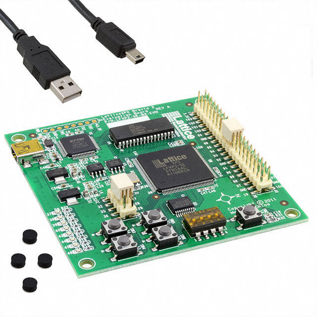
iCEblink40-HX1K Evaluation Kit User’s Guide September 2012 Revision: EB73_01.1
iCEblink40-HX1K Evaluation Kit User’s Guide Introduction Thank you for choosing the Lattice Semiconductor iCEblink™40-HX1K Evaluation Kit. This guide describes how to begin using the iCEblink40-HX1K Evaluation Kit, an easy-to-use platform for rapidly prototyping designs using the iCE40 FPGA. Features (cid:129) High-performance, low-power iCE40HX1K FPGA (cid:129) USB programming, debugging, virtual I/O functions, and power supply (cid:129) Four user LEDs (cid:129) Four capacitive-touch buttons (cid:129) 3.3 MHz clock source (cid:129) 1Mbit SPI serial configuration PROM (cid:129) Supported by Lattice iCEcube2™ design software (cid:129) 68 LVCMOS/LVTTL (3.3V) digital I/O connections on 0.1” through-hole connections (cid:129) Supports third-party I/O expansion boards and modules, including 3.3V Arduino Shield boards (requires addi- tional sockets, not supplied) Figure 1. iCEblink40-HX1K Evaluation Board and Major Hardware Features USB Programming, Low Power iCE40 68 User I/O Pins Debug and Power FPGA (3.3V) Capacitive Touch Buttons User LEDs Software Requirements Before using the iCEblink40 board, please be sure to download and install iCEcube2 release 2011.12 or later. This and later versions include the programming software for the iCEblink40 board. Currently, the programming software is only available for the Windows operating system. http://www.latticesemi.com/products/designsoftware/icecube2/downloads.cfm During the installation process, be sure to install the Adept USB Programming Software, as shown in Figure 2. 1. Make sure that Adept USB Programming Software is checked. This is the default setting. 2. Click Next. 2
iCEblink40-HX1K Evaluation Kit User’s Guide Figure 2. Select the Adept Programming Software for Installation 1 2 A few steps later, select the installation for the Adept programming software, as shown in Figure 3. 3. Make sure that both the Adept Runtime and Adept Application options are checked, which are the default settings. 4. Click Next. Figure 3. Adept Setup Options 3 4 Connecting to the iCEblink40 Evaluation Board Before connecting the iCEblink40 board, be sure to download and install a supported version of the iCEcube2 soft- ware. Connect the iCEblink40 evaluation board to your PC using the USB cable provided. The USB connector on the board is labeled with reference designator J3 and is located in the upper left corner. Once connected, the red power-good LED (LD1) adjacent to the USB connector illuminates. See Figure 4 to locate the power-good LED. 3
iCEblink40-HX1K Evaluation Kit User’s Guide Power and Configuration Status LEDs The iCEblink40 evaluation board has two status LEDs, as shown in Figure 4. These two status LEDs indicate the current status of the iCEblink40 board, as listed in Table 1. The red LED, LD1, located near the USB connector indi- cates if the USB power supply, the 3.3V supply, and the 1.2V supply are within the specified ranges. The yellow LED, LD6, located below the FPGA indicates whether the FPGA is configured properly. This LED lights up when the FPGA is correctly loaded with a valid bitstream. Figure 4. iCEblink40 Status LEDs Power-Good LED (LD1) (Red LED) iCE40HX1K VQ100 FPGA Configuration Done LED (LD6) (Yellow LED) Table 1. iCEblink40 Status LED Descriptions Power-Good Configuration DONE LED (LD1) LED (LD6) Description The board is powered, the FPGA successfully configured and the FPGA On On application is operating. Board is unpowered. Connect the board to a computer USB port, a pow- ered hub, or a USB-based wall plug. Off Off If board is plugged in and previously operating, indicates that an SPI Flash programming operation is in progress The board is powered but the FPGA is not yet configured. On Off ACTION: Program the onboard SPI Flash PROM with a valid FPGA configuration bitstream. ERROR: The board is powered but there is a problem with the USB Off On power supply or with the on-board regulator. 4
iCEblink40-HX1K Evaluation Kit User’s Guide Pre-programmed Demonstration Design The iCEblink40 board comes preprogrammed with a demonstration application. The application supports two inter- faces. 1. Control the LEDs from the four capacitive touch buttons on the board itself. 2. Control the LEDs and other internal logic using the USB-based I/O expansion interface. Operating the Capacitive Touch Buttons Upon power up, the green LEDs on the board scroll in an upward pattern, as described in Figure 5. Pressing any of the capacitive touch buttons stops the LEDs from scrolling and places the board in a different operating mode. Figure 5. Preprogrammed Demonstration Design LEDs Scroll Upward 1. Power On Green LEDs scroll upward. 2. Press any button to enter LED Toggle Mode. Toggle LED with Button Press 3. Press a button to toggle the associated LED on or off. If no button is pressed within five seconds, the board returns to Scroll LEDs Mode. In the second operating mode, toggle individual LEDs on and off by pressing the associated capacitive touch but- ton. If no button was pressed during the last five seconds, the board returns to scrolling the LEDs. The demonstration application is available for download from the Lattice website at: www.latticesemi.com/iceblink40-hx1k. Virtual I/O Expansion Debugging Interface The iCEblink40 board is powered and programmed via the USB interface. Additionally, the USB interface also pro- vides a convenient means to monitor and control logic inside the FPGA, as shown in Figure 6. The USB controller drives a byte-wide parallel port expander implemented within the FPGA, controlled by software running on the PC. The Digilent ADEPT2 I/O Expansion screen, shown in Figure 7, provides a mix of virtual switches, pushbuttons, LEDs, light bars, and 32-bit input and outputs. 5
iCEblink40-HX1K Evaluation Kit User’s Guide Figure 6. iCEblink40 Board Supports Virtual I/O Connections over USB Debug I/O E xpansion Core Debug I/O Expansion Core DB LEDs[7:0] Data[7:0] LightBar[23:0] ASTB Address Strobe USB DSTB FromFPGA[31:0] To/From Data Strobe Controller Switches[15:0] FPGA WRITE Read/#Write Buttons[15:0] WAIT Wait ToFPGA[31:0] FPGA Control and monitor FPGA logic values in real-time, over USB, from PC graphical interface Digilent Adept 2 Figure 7. Digilent Adept 2 I/O Expansion Interface and FPGA Connections VLightBar To FPGA [31:0] From FPGA [31:0] 23 0 VLEDs 7 6 5 4 3 2 1 0 15 14 13 12 11 10 9 8 15 14 13 12 11 10 9 8 VButtons VSwitches 7 6 5 4 3 2 1 0 7 6 5 4 3 2 1 0 Using the Virtual I/Os in the Demo Application By default, the virtual I/Os are disconnected and the USB controller’s I/O connections to the FPGA are high-imped- ance (Hi-Z). To connect the virtual I/O, perform the following steps outlined in Figure 8. 1. From the Windows Start menu, select Start > All Program > Digilent > Adept > Adept. 2. Ensure that the Adept interface connects to the iCE40. 3. Click the I/O Ex tab. 6
iCEblink40-HX1K Evaluation Kit User’s Guide 4. Click Start I/O. Remember, the associated I/O Expander design must be part of the compiled FPGA design before the Virtual I/Os work. 5. If the virtual I/O expansion design is functioning correctly, the green virtual status LED will turn from red to green. Figure 8. Starting the Digilent Adept Virtual I/O Expansion Application 2 3 4 5 To disconnect the virtual I/O interface, simply click the Stop I/O button in the graphical interface. Controlling the Physical LEDs from Virtual I/Os in the Demonstration Design When active, the virtual I/Os optionally control the physical LEDs on the board, as shown in Figure 9. For example, with the virtual I/Os active, change the position of virtual switch [7] (the bottom left switch in the graphical interface). Note how the physical LEDs on the board change direction. Change virtual switch [6] to the up position. Now, the physical LEDs are controlled by the virtual switches [3:0] and virtual pushbuttons [3:0]. The values of the virtual switches are XORed together inside the FPGA. The virtual slide switches set a specific value for the physical LEDs. The pushbutton momentarily inverts the value while the virtual pushbutton is pressed in the graphical interface. 7
iCEblink40-HX1K Evaluation Kit User’s Guide Figure 9. Controlling the Physical LEDs from Virtual I/O Virtual Switches Virtual Pushbuttons [7] [3] [2] [1] [0] [6] 1: Scroll down [3] [2] [1] [0] 1: Control LEDs from Virtual I/Os 0: Scroll up 0: Control LEDs from FPGA LD2 BTN1 LD3 BTN2 Physical Buttons and LEDs LD4 BTN3 LD5 BTN4 Direction Controlling the Virtual Light Bar in the Demonstration Design When the virtual I/Os are active, the virtual light bar lights up from left to right, controlled by logic inside the FPGA. The virtual pushbuttons [15] and [14] control the light bar. Pushbutton [15] resets the light bar, clearing all the lights. Pushbutton [14] forces the light bar to hold its current value. Figure 10. Controlling the Virtual Light Bar Lights Up from Left to Right Light Bar [15] [14] Reset Hold Light Value Bar Controlling the Virtual LEDs in the Demonstration Design The virtual I/O interface includes eight, round, green LEDs, as shown in Figure 11. The values displayed on these virtual LEDs depends on the settings of virtual switches [9] and [8]. The eight LEDs are separated into left and right halves. When both virtual switches [9] and [8] are Low—the down position—the left LEDs echo the scrolling pattern of the LEDs, regardless if a physical cap-sense button was pressed. Use virtual switch [7] to reverse the direction of these LEDs. The right-most LEDs show the current toggle status of the four physical cap-sense buttons. Changing virtual switch [8] to High—the up position—the four left-most LEDs then show the current value of the time-out counter than marks the five seconds after pressing a cap-sense button. Press a cap-sense button to reset the timer and note that the toggle status of the physical button changes on the right-most LEDs. The timer resets each time a physical button is pressed. Wait five seconds and the physical LEDs change back to the scrolling pat- tern. 8
iCEblink40-HX1K Evaluation Kit User’s Guide Figure 11. Controlling the Virtual LEDs LEDs [9] [8] Scrolling LED Toggle value pattern of physical cap-sense buttons [9] [8] (push button to Cap-sense change) time-out counter [9] [8] [3] [2] [1] [0] [3] [2] [1] [0] When virtual switch [9] is High—in the up position—then the left LEDs are controlled by virtual switches [3:0] and the right LEDs are controlled by virtual pushbuttons [3:0]. Virtual Values to and from FPGA in the Demonstration Design The virtual I/O interface also includes a 32-bit value from the FPGA logic and a 32-bit value to the FPGA logic, as shown in Figure 12. Two virtual switches, [14] and [15], control the behavior in of the virtual 32-bit values in the demonstration design. Figure 12. Virtual Values To and From the FPGA To FPGA From FPGA [13] 0x1000ffff efff0000 Send Format: Hexadecimal Reset [15] [14] Continuously No function increment [15] [14] Continuously No function decrement [15] [14] One’s complement Input value of input value [15] [14] Reverse bit order Input value of input value Clocking Resources The iCEblink40 board includes a Linear Technology LT1799 oscillator (X1 on the board and in the schematic) to generate a 3.33 MHz clock. FPGA Input The output from the LT1799 oscillator feeds pin 13 of the iCE40HX1K FPGA. FPGA pin 13 is also the global buffer input GBIN7. 9
iCEblink40-HX1K Evaluation Kit User’s Guide Supporting Other Frequencies On the iCEblink40 board, the LT1799 produces a 3.3 MHz clock output by default. Other frequencies are possible via simple modifications of the board using the 1x3 connections on JP2, as listed in Table 2. Table 2. Selecting Other Oscillator Frequencies Using Jumper JP2 Clock Frequency JP2 Setting Jumper Position 3.33 MHz (default) None 333 kHz Upper Position 33.3 MHz Lower Position User LEDs The iCEblink40 iCE40HX1K evaluation board includes four green user LEDs, located along the left side of the board, as shown in Figure 1. Operation To light a user LED, drive the associated FPGA pin High, as shown in Table 3. To darken the LED, drive the associ- ated FPGA pin Low. Table 3. User LED Operation Operation FPGA Action Light LED Drive High (1) Darken LED Drive Low (0) The LEDs may appear to glow slightly before the FPGA is configured or if the FPGA pin is unused. This is because the FPGA I/Os have a soft pull-up resistor which may provide just enough current for the LED to glow dimly. To completely turn off an LED, drive it Low. FPGA Connections The FPGA drives the user LEDs using the FPGA pins listed in Table 4. These same signals also connect to the J12 header located in the lower left corner. 10
iCEblink40-HX1K Evaluation Kit User’s Guide Table 4. User LED Connections Designator Location FPGA Pin Header Connections LD2 LD2 [59] 59 J12.1 LD3 LD3 [56] 56 J12.2 LD4 LD4 [53] 53 J12.3 LD5 LD5 [51] 51 J12.4 Capacitive Touch Buttons The iCEblink40 iCE40HX1K evaluation board has four capacitive-touch buttons, located toward the left side of the board, as shown in Figure 1. These buttons have dedicated connections only to the FPGA. These signals go nowhere else on the board and are not available on any of the breakout headers. FPGA Connections Table 5 lists the four capacitive touch buttons on the iCEblink40 board and the associated FPGA pins. Table 5. Capacitive Touch Buttons Designator Location FPGA Pin BTN1 BTN1 [60] 60 BTN2 BTN2 [57] 57 BTN3 BTN3 [54] 54 BTN4 BTN4 [52] 52 Operation Figure 13 shows the circuit used for each capacitive-touch button. Each button is attached to one I/O pin on the FPGA. Each signal line includes a 100 k pull-up resistor to 3.3V and a 100 pF capacitor down to ground. Figure 13. Example Capacitive Touch Button Circuit I/O Pin Capacitive Sample Touch Button 100 kΩ Value 100 pF Figure 15 shows the general overall flowchart for the demonstration design to read the value on a capacitive touch button. The sampling signal drives the voltage on the capacitive-touch button to ground in order to bleed of any residual charge as shown in Figure 14. After a period of time, depending on the button sample frequency, the button is allowed to float High. Once the FPGA output goes to Hi-Z (high-impedance, floating, three-state), the 100k pull-up resistor to 3.3V charges the 100 pF capacitor. After about an RC time constant ( or tau), the voltage on the pad exceeds the input switching threshold of the FPGA. A finger pressed against the capacitive-touch button adds about another 5 pF of capacitance, increasing the RC constant and delaying the Low-to-High transition for a pressed button. 11
iCEblink40-HX1K Evaluation Kit User’s Guide Figure 14. Capacitive Touch Timing Examples Sampling Allow pad to Signal Drive pad to ground float High Button: No Finger SThwrietcshhionlgd τ = RCBUTTON Button Value: Time delta between No Finger pressed and unpressed button ~300-500 ns Button: Finger Press SThwrietcshhionlgd τ = R(CBUTTON + CFINGER) Button Value: Finger Press The switching time difference between an unpressed and one or more pressed buttons is roughly 300 to 500 ns. Using the 3.33 MHz input, this amounts to a one clock delay difference between an unpressed and pressed but- tons. The simple circuit used on the iCEblink40 board detects simultaneous button presses on up to three of the capaci- tive-touch buttons. Pressing all four buttons is the same as pressing no buttons. 12
iCEblink40-HX1K Evaluation Kit User’s Guide Figure 15. iCEblink40 Demo Application Capacitive Touch Button Flowchart Start Drive pin connected to capacitive button Low long enough to guarantee that the pin is at GND, despite the attached RC network. Force pin to Hi-Z. The external pull-up resistor pulls the pin High and charges the capacitor. Did any pin go High? Yes Wait one 3.3 MHz clock period (300 ns). Sample all pin values. Are all Yes buttons High? Did pin No value change from last sample? Yes Toggle pin value 13
iCEblink40-HX1K Evaluation Kit User’s Guide User I/O Connections Figure 16 shows the location of the 3.3V-compatible digital I/O connections on the iCEblink40 board. Each connec- tion shows the pin number of the FPGA I/O pin that attaches to the connection. Likewise, Table 6 lists the various I/O headers and their designed usage. Figure 16. Location of the 3.3V Digital I/O Connections and the FPGA Pin Number Digital I/O (3.3V) 3.3V Arduino Shield Compatible 8]ND2]9]6]4]1]9] 6]3]1]9]4]2]9] 6] 1G199998 8887776 6 [ [[[[[[ [[[[[[[ [ Digital I/O (3.3V) 3.3V 9]6]5]0]7]5]3]0] 7]5]2]0]8]3]1]8] 11109999 88887776 GND [[[1[[[[ [[[[[[[[ SPI PROM [1] [7] [ Connections [2] [8] [3] [9] [49] [4] [10] [45] 2 [46] 1 PMOD PMOD D [48] O PMOD12 M GND P ble 3.3V 3.3V u o GND PMOD D [33] [20] [28] [21] [27] [24] [26] [25] PMOD PMOD PMOD12 ND3V1]3]6]9] D [13] 0]6]0]2]2]4]ND3V D G3.[5[5[5[5 MO [33] [3[3[4[4[6[6G3. MO 2 P P 1 D Clocks O M User LEDs D P ]]]]]] O 947135 M 233466 P Double PMOD 12 Double-wide Digilent 2x6 Header [[[[[[ PMOD12 Digilent 2x6 Header Digital I/O (3.3V) PMOD Digilent 1x6 Header 14
iCEblink40-HX1K Evaluation Kit User’s Guide Table 6. Digital I/O Headers and Their Functions I/O Header Header Group Type Location Function J2 2x8 0.1” centers Top edge, middle 3.3V digital I/O. Compatible with 3.3V Arduino Shield boards. J4 2x8 0.1” centers Top edge, left side 3.3V digital I/O. Compatible with 3.3V Arduino Shield boards. 3.3V digital I/O. 3.3V digital I/O. Compatible with Digilent 1x6 and J1 2x6 0.1 centers Left edge, top 2x6 PMod modules. Also supports double PMod12 modules when used with header J6. 3.3V digital I/O. Compatible with Digilent 1x6 and 2x6 PMod mod- J6 2x6 0.1 centers Left edge bottom ules. Also supports double PMod12 modules when used with header J1. J7 1x6 0.1 centers offset Left edge, top Production programming of USB controller. 3.3V digital I/O. Connections between the mobile FPGA and the J11 1x6 0.1 centers offset Middle, toward left SPI PROM. Compatible with Digilent 1x6 PMod modules. 3.3V digital I/O. Portions compatible with Digilent 1x6 and 2x6 J5 2x8 0.1” centers Bottom edge, right side PMod modules. Portions also compatible with 3.3V Arduino Shield boards. Middle, to left of 3.3V digital I/O. Clock connections from the LTC1799 oscillator JP3 1x2 0.1” centers FPGA (GBIN7) and possible into GBIN2. 3.3V digital I/O. Connections to the user LED I/O. Compatible J12 1x6 0.1” centers Bottom edge, left side with Digilent 1x6 Pmod modules. Supported Pmod Peripheral Modules As shown in Figure 16, the iCEblink40 board supports a variety of Pmod peripheral modules for easy I/O expan- sion. Table 7 lists the 0.1” through-hole headers on the iCEblink40 board that support Pmod modules. Pmod mod- ules come in a few different form factors and each Pmod header includes power and ground supplies. Figure 17 shows the how the different Pmod form factors interrelate. The easiest way to support a Pmod module is to add the appropriate female socket listed, or an equivalent. Straight-through or right-angle through-hole sockets are listed. Male headers are also possible solutions when using the interface cable provided with most Pmod modules. Table 7. Pmod Module Headers Female Socket (Manufacturer/Part Number) Header Type Straight-through Right-angle 2x6 header on 0.1” centers. Each is a Pmod12 header that Sullins Connector Sullins Connector J1, J12 supports two six-pin Pmod modules. Both together form a Solutions Solutions double-wide Pmod connection. PPPC062LFBN-RC PPPC062LJBN-RC 2x8 header on 0.1” centers. The left side of header J5 forms Sullins Connector Sullins Connector a Pmod12 header, as shown in Figure 16. A 2x6 header sim- J5 Solutions Solutions ilar to J1, J12 can also be used but must be mounted toward PPPC082LFBN-RC PPPC082LJBN-RC the right end of the holes as marked. As shown in Figure 17, a Pmod module has six connections—four I/O plus power and ground. A Pmod12 module has 12 connections and the module is effectively two six-pin Pmod modules stacked together. Finally, a double- wide Pmod12 consists of two Pmod12 headers spaced apart. Most of the Pmod modules also include interface cables to allow easy connection to other header types. 15
iCEblink40-HX1K Evaluation Kit User’s Guide Figure 17. Pmod Module Types Pmod12 Pmod D V N 3 I/O G 3. d D V o I/O N 3 m 2 G 3. P d1 o 1 1 d m mo P P Double-wide Pmod12 D V D V N 3 N 3 I/O G 3. d I/O G 3. d o o m 2 m 2 P d1 P d1 1 d mo 1 d mo mo P mo P P P For a complete list of Pmod peripheral modules, visit the Digilent web site. www.digilentinc.com/Products/Catalog.cfm?NavPath=2,401&Cat=9 Arduino Shield Board Support The iCEblink40 board also mechanically and electrically supports select 3.3V Arduino Shield boards popular in the microcontroller development community. The Shield connections are located on headers J4, J2, J8 and a portion of J5 as shown in Figure 18. Headers jumper J4 and J2 are 3.3V digital I/O connections. Header J8 provides power connections to the Shield board. The left side of header J5 also provides 3.3V digital I/O but the 3.3V and GND connections do not connect to the Shield board. Figure 18. Arduino Shield Board Connections Arduino Shield Connections iCE40HX1K VQ100 Required Header Sockets To support Arduino Shield boards, the indicated headers must be loaded with female socket headers on 0.1” head- ers, as listed in Table 19. 16
iCEblink40-HX1K Evaluation Kit User’s Guide Table 8. Sockets to Support Arduino Shield Boards Header(s) Description Quantity Manufacturer/Part Number Sullins Connector Solutions J2, J4, J5 2x8 female header socket on 0.1” centers 3 PPPC082LFBN-RC Sullins Connector Solutions J8 1x6 female header socket on 0.1” centers 1 PPPC061LFBN-RC Tested Arduino Boards Figure 19 shows the Arduino Shield boards have been tested for basic compatibility. Other Arduino Shield boards may also be compatible. Figure 19. Compatible Arduino Shield Boards chipKITBasic I/O Shield chipKIT Pmod Shield-Uno USB Interface The iCEblink40 board is powered by connecting the board to a computer USB port, a power USB hub, or a USB- based AC adapter, commonly used in consumer electronics. A typical USB port provides up to 500 mA at 5V, pro- viding up to 2.5W of total power. The iCE40HX1K consumes SIGNIFICANTLY LESS power, even when operating at full performance. However, be careful when using the board to power off-board peripheral funds. Connector The USB connector to the board is located in the upper left corner, labeled J3. The board connects using a stan- dard USB cable with a male mini-B connector. Power Supply Figure 20 shows the iCEblink40 power supply circuit that derives power from the USB mini-B connector (J3). The USB connector provides up to 500 mA at +5V DC. An Analog Devices ADP2140 regulator generates +1.2V for the FPGA core VCC and +3.3V for all I/O connections. The regulator also indicates when power is good and lights up the red power-good LED (LD1). 17
iCEblink40-HX1K Evaluation Kit User’s Guide Figure 20. iCEblink40 USB Power Supply Circuit Power-Good LED (LD1) Mini-B USB +5V Connector (J3) (500 mA) Analog Devices (JP1) iCE40HX1K ADP2140 +1.2V VCC Voltage (300 mA) FPGA Regulator +3.3V VCCIO (600 mA) Configuration Done LED (LD6) Jumper JP1 provides a convenient location from which to measure core power to the FPGA. SPI Flash Programming The USB interface also provides Flash programming for the on-board SPI PROM, as described in “Programming the iCEblink40 Board” below. Digilent Parallel Port (DPP) The Digilent Parallel Port (DPP) interface is used for virtual I/O and debugging using a USB connection to the board from a Windows PC. See “Virtual I/O Expansion Debugging Interface” on page 5 for additional information. 1Mbit SPI Configuration PROM The configuration bitstream for the iCE40 FPGA is stored in a M25P10A 1Mbit SPI serial Flash PROM. The PROM is large enough to hold two configuration images and supports the iCE40 WarmBoot feature, if so enabled within the FPGA application. The PROM is physically located on the back side of the board. Programming the iCEblink40 Board The iCEblink40 board includes on-board USB-based programming support either from the Lattice iCEcube2 soft- ware or using a command from a console window or DOS box. From iCEcube2 Figure 21 shows the command sequence for programming the SPI Flash PROM on the iCEblink40 board using the iCEcube2 development software. 18
iCEblink40-HX1K Evaluation Kit User’s Guide Figure 21. Programming the iCEblink40 Board from iCEcube2 3 1 4 2 5 6 1. Select Tool > Programmer from the iCEcube2 menu bar. 2. Click the dropdown button ( ) under Programming Hardware. 3. Select iCEblink40. 4. The bitstream file should already be set appropriately based on the iCEcube2 project settings. If not, click Image Files Settings to select the configuration bitstream file. 5. Click Execute to program the iCEblink40 board. If all is working correctly, the power-on LED and the configuration done LED will both go out momentarily as iCEcube2 programs the on-board SPI Flash PROM. After programming is complete, both LEDs should light up again and the FPGA will execute the new configuration image. From Command Line The iCEblink40 programming software can also be executed from a console window or DOS box. To open a con- sole window or DOS box, click the Start button and type cmd in the textbox immediately above the Start button. Executable Location After installation, the programming software executable is called iceutil.exe and is located in the \Sbt- Tools\sbt_backend\bin\win32\opt directory. The iecutil.exe executable can be copied into the same directory as the FPGA bitstream image or can be pointed to on the command line. FPGA Bitstream Configuration File The required bitstream image is part of the iCEcube2 project. Multiple versions of the bitstream are stored in the <projname>_Implmnt\sbt\outputs\bitmap directory. The raw hexadecimal version of the bitstream is called <projname>_bitmap.hex. The alternate format of the same information is an Intel hexadecimal file called <proj- name>_bitmap_int.hex. Raw Hexadecimal Command Example <path>/iceutil -d iCE40 -res -cr -m M25P10A -fh -w <path/projname>_bitmap.hex Intel Hexadecimal Command Example <path>/iceutil -d iCE40 -res -cr -m M25P10A -fi -w <path/projname>_bitmap_int.hex 19
iCEblink40-HX1K Evaluation Kit User’s Guide Help <path>/iceutil -help Testing Core Power Jumper JP1 provides the ability to measure core power consumption by the FPGA. Two power measurement meth- ods are supported. Note: The iCEblink40 HX1K evaluation board uses an early version of the iCE40HX1K silicon that has higher than expected static current consumption. Although the demonstration application consumes less than 500 µA, the pro- duction silicon will consume even less current. Similarly, the lower power iCE40LP1K devices use even less power than the iCE40HX1K FPGA. Easy Method Using a Multimeter Connect the iCEblink40 board through your high-accuracy multimeter. Use a meter with a minimum of 10,000 counts; 50,000 counts or more is recommended for better accuracy. To take a quick measurement, follow these steps. 1. Disconnect power to the iCEblink40 board by removing the USB cable connection, either at the board or at the computer. 2. Remove the jumper JP1, which isolates the FPGA’s core supply from the 1.2V supply on the board. 3. Connect your multimeter’s alligator or test clips to the stake pins on header JP1. 4. Configure the multimeter to measure current using its highest mA or Amp range. This setting typically has the lowest voltage drop internally within the meter. 5. Re-connect the USB cable that supplies power to the iCEblink40 board and configure the FPGA device if nec- essary. 6. Observe the power reading on the multimeter. At low clock rates, which results in lower power consumption, switch the meter to a lower amperage setting for better accuracy. However, this also may increase the resis- tance across the meter leads. Using too low of a meter setting causes a large voltage drop within the meter, potentially violating the minimum input voltage specification to the FPGA device. 7. The value measured by the multimeter is a current. Convert the measurement to power using Equation 1. The voltage is the operating voltage, the voltage across the jumper. This value can be accurately measured with a second multimeter to show the voltage drop across the first. However, just measuring the initial voltage, before taking any current readings, usually provides acceptable accuracy and the voltage drop across the meter is generally small. Power = CurrentVoltage (1) Although this method is easy, here are a few caveats and pointers. (cid:129) Always start at the highest current setting for your meter. Using too small a setting may damage your meter! After determining the maximum current range for your measurement, then you can safely use the appro- priate lower current setting. (cid:129) The voltage drop across the meter leads may violate the minimum supply voltage specification for the mobile- FPGA device. To determine the voltage drop, use a second multimeter to measure either the voltage across the first meter’s leads during a test or the resistance between the first meter’s leads. (cid:129) Using the highest current measurement setting typically results in the lowest voltage drop. 20
iCEblink40-HX1K Evaluation Kit User’s Guide Using High-Precision, Small-Value Resistors For more-accurate, time-sensitive measurements, place a low-value resistor across the jumper test point. Accord- ing to Ohm’s Law, the current passing through the resistor produces a voltage drop. Measure the voltage differen- tial across the resistor during expected operation. Convert the measurement to power using Equation 2. The voltage is the measured voltage across the resistor; the resistance is the value of the resistor. 2 Voltage Power = ---------------------------- (2) Resistance The following are a few guidelines on selecting a resistor. (cid:129) Use a high-precision resistor. (cid:129) The resistor must handle the power dissipated under the anticipated test conditions. (cid:129) Too small a resistor value may result in too small a voltage difference across the resistor to measure with your test equipment. (cid:129) Too large a resistor value may result in too large of a voltage difference across the resistor. Too large a voltage drop might violate the minimum voltage specifications for the FPGA device. Figure 22 shows an example header block designed to fit over one of the jump locations. Measure the voltage drop across the low-value resistor, either with a voltmeter or with data acquisition equipment. Figure 22. Resistor Header Block Voltmeter Low Ω, High Precision Resistor This method is recommended for taking power measurements over time. Mechanical Specifications Figure 23 shows the mechanical dimensions for the iCEblink40 board, including the location of the four mounting holes. With a jumper installed on JP1, the board height is approximately 0.700 inches high, including the four rub- ber feet mounted on the bottom side of the board. 21
iCEblink40-HX1K Evaluation Kit User’s Guide Figure 23. iCEblink40 HX1K Board Mechanical Dimension iCE40HX1K VQ100 Ordering Information China RoHS Environment-Friendly Description Ordering Part Number Use Period (EFUP) iCEblink40-HX1K Evaluation Kit ICE40HX1K-BLINK-EVN Technical Support Assistance Hotline: 1-800-LATTICE (North America) +1-503-268-8001 (Outside North America) e-mail: techsupport@latticesemi.com Internet: www.latticesemi.com Revision History Date Version Change Summary May 2012 01.0 Initial release. September 2012 01.1 Nomenclature change from “mobileFPGA” to “FPGA”. © 2012 Lattice Semiconductor Corp. All Lattice trademarks, registered trademarks, patents, and disclaimers are as listed at www.latticesemi.com/legal. All other brand or product names are trademarks or registered trademarks of their respective holders. The specifications and information herein are subject to change without notice. 22
iCEblink40-HX1K Evaluation Kit User’s Guide Appendix A. Schematic Figure 24. Schematic A B C D 123456 Mechanically compatible with Basic I/O shield.USB Mini ABUSB5V0VCC_3V3Power Measurement Test PointS1S3NOT STUFFEDNOT STUFFEDSHUNTNOT STUFFEDS1S3VCC_1V2VCC_CORE5GNDG1x6R40iCE40-CRESET4No LoadR1ID1C113559731559713140263D+USB5V0VCC_3V3VCC_3V3ADP2140ACPZ3312R7111000001000100D4.7KBBBB0D+8.2uF2---------------EDD2D2D222222111111124D-2106VCC_3V3DF--CCCCCCCCCCCCCCC----D-VIN1VOUT2VIN1VOUT23DD0000NFSSSSSSSSSSSSSSS15USB5V0DL14444UOODDDDDDDDDDDDDDDGVVIN2VIN24JP1EEEENS2S429iCE40-CRESETGNDMMTCCCCGS2S4SWPGSWPG5SDDIIiiiiUSB5V08DDUSB-ON 1uHTEN1EN16DDNNNNOJ347NNGGR3GGJ4J2J5FBEN2FBEN2NJ8357913713595135913571351GGAAPP11111111110888IC1xxxR4044246206062C3C4C222213P611111218111248624116418GND1M1nF/250V10uF1uFPower-On LEDLD1VCC_3V3VCC_3V3D436201845974366209285104826648204621357NGND10110100000010111000101001111101000BBBBG-----------------------------------22122111222211222221121122211111111DDDD13--CCCCCCCCCCCCCCCCCCCCCCCCCCCCCCCCCCC----DD0000SSSSSSSSSSSSSSSSSSSSSSSSSSSSSSSSSSS4444OODDDDDDDDDDDDDDDDDDDDDDDDDDDDDDDDDDDEEEEGNDGNDMMCCCCIIiiiiBTN1R2C8C6C7C90100K957670134801256909310nF1uF0.1uF10nF89889997788889999185%R6iCE40-SS_B1CapButtonCapButtonoo00000000000000000000000000000000000000CAPBTN1AT90USB2OOOOOOOOOOOOOOOOOOOOOOOOOOOOOOOOOOOOOO75R7IIIIIIIIIIIIIIIIIIIIIIIIIIIIIIIIIIIIII14iCE40-SCKUSB-SS_BPPPPPPPPPPPPPPPPPPPPPPPPPPPPPPPPPPPPPPPB0/SS/PCINT0////01101588USB-SCKVCC_3V3GND75NNNNPB1/SCLK/PCINT1C5VCCIO_0VCCIO_0R5R8iCE40-SONo LoadUSB-MOSILED11692IIIIBBBBPB2/PDI/MOSI/PCINT2100pFVCCIO_0VCCIO_017USB-MISOGGGG200390PB3/PDO/MISO/PCINT3C12C10C13C14C11C15C17C18C16R10LD2iCE40-SI18IC2EPB4/T1/PCINT410nF1uF10nF10nF0.1uF1uF10nF10nF0.1uFiCE40VQ10019200PB5/PCINT520iCE40-CRESETGNDVCC_COREPB6/PCINT621PB7/OC0A/OC1C/PCINT7iCE40-CDONENOT STUFFEDIC3AAT90USB2-16MUGNDGND421x6C19C20C24C25C21C26C23C22612LED1781uF1uF10nF10nF0.1uF10nF10nF0.1uF1651VCC_3V3AT90USB2LED2PMOD2-4PIO3/DP00APIO3/DP00A2333333274LED3DSC2-07PMOD2-3______PIO3/DP00BPIO3/DP00BPIO1PIO13OOOOOO1111LED4DSC2-06PMOD2-2IC2FVCC_3V3373____IIIIIIPIO3/DP01APIO3/DP01APIO1PIO14R12OOOOCCCCCC5472115DSC2-05PMOD2-1iCE40-ASTBGNDUSB-ONCCCCCCIIIIPC2/PCINT11PIO3/DP01BPIO3/DP01BPIO1PIO1VCCGNDVCCGND5CCCCVVVVVVDSC2-04PMOD1-47713517CCCC200PIO3/DP02APIO3/DP02APIO1PIO1VCCGNDVCCGND6R13VVVVDSC2-03iCE40-DSTBUSB-ASTBBTN2268696123PMOD1-3R9PC4/PCINT10PIO3/DP02BPIO3/DP02BPIO1PIO1VCCGNDVCCGNDJ12DSC2-02USB-DSTBPMOD1-2259687732100K200PC5/OC1B/PCINT9PIO3/DP03APIO3/DP03APIO1PIO1VCCGNDVCCGNDR14DSC2-01iCE40-WRITE23USB-WRITE1066395%PMOD1-1PC6/OC1A/PCINT8PIO3/DP03BPIO3/DP03BPIO1PIO1GNDGND22USB-WAIT1126547GNDIMOD-1DSC1-11200PC7/INT4/ICP1/CLK0CapButtonCapButtonooPIO3/DP04APIO3/DP04APIO1PIO1GNDGNDR15iCE40-WAITCAPBTN2136455SYSCLKIMOD-2GBIN7/PIO3/DP04BGBIN7/PIO3/DP04BPIO1PIO1GNDGNDIC3BAT90USB2-16MU156370IMOD-3DSC1-12200D1GBIN6/PIO3/DP05AGBIN6/PIO3/DP05AGBIN2/PIO1GBIN2/PIO1GNDGNDR16iCE40-DB016627584IMOD-4DSC1-14PIO3/DP05BPIO3/DP05BGBIN3/PIO1GBIN3/PIO1VPP_2V5GNDVPP_2V5GNDC27R11No LoadLED218607698DSC1-15CAPBTN1200100pFPIO3/DP06APIO3/DP06APIO1PIO1VPP_FASTGNDVPP_FASTGNDR17SB0503EC-TRiCE40-DB11959DSC1-16LED1390PIO3/DP06BPIO3/DP06BPIO1PIO1LD3iCE40VQ100AT90USB2GND2057PMOD3-4CAPBTN2200PIO3/DP07APIO3/DP07APIO1PIO1R19iCE40-DB2USB-DB0PMOD3-362156LED2iCE40HX1KPD0/OC0B/INT0PIO3/DP07BPIO3/DP07BPIO1PIO1USB-DB1GND72454PMOD3-2CAPBTN3200PD1/AIN0/INT1PIO3/DP08APIO3/DP08APIO1PIO1R20iCE40-DB3USB-DB2GND82553PMOD3-1LED3PD2/RXD1/AIN1/INT2PIO3/DP08BPIO3/DP08BPIO1PIO1USB-DB3952CAPBTN4200PD3/TXD1/INT3PIO1PIO1R21iCE40-DB4USB-DB410IC2AiCE40VQ10051LED4PD4/INT4PIO1PIO1USB-DB511200PD5/XCK/PCINT12R23iCE40-DB5USB-DB6VCC_3V312IC2DiCE40VQ100PD6/RTS/INT6USB-DB713200PD7/CTS/HWB/T0/INT7R24iCE40-DB6C29C31C32C30IC3CAT90USB2-16MUIC2CiCE40VQ1002001uF10nF10nF0.1uFR25iCE40-DB750SPI_VCCSPI_VCCBTN3IC2BiCE40VQ100R18200NOT STUFFED31100KBB1x6VCCIO_2VCCIO_2KK0101__38ISP-RESET5%OOCCSS1VCCIO_2VCCIO_2LLLL2222IISSSSSSSSVCC_3V31GNDUSB-MOSIOOOOEEEEBBBasic oscillator________2CapButtonCapButtonoo__SSSSIIIIIIIIIIIICAPBTN3X1USB-MISOPPPPTTBBBBPPPPPPPPR26R27EE////3EECCCC5454SSSSSSSSNN15SYSCLKUSB-SCK////////////////////////SSNNNN4.7K4.7K22222222222222222222SSSSSSSSC34C334V+OUTV+OUTOOEEIIIIOOOOOOOOOOOOOOOOOOOOOOOOOOOOGNDNOT STUFFEDDDBBBBRR510nF1uFC28R22R28IIIIIIIIIIIIIIIIIIIIIIIIIIIIGGGGCCCCPPPPPPPPPPPPPPPPPPPPPPPPPPPPNOT STUFFEDNo LoadLED3USB3V336C35100pFSETSETVCC_3V3iCE40-WAIT3903.0K0.1uFLD4J7685879361349047026DIV24SYSCLK444222333344444234GNDDIVGNDDIVGNDJP3LTC1799CS5#TRPBFGNDGNDiCE40-SS_BJP2Atmel USB Programming BlockiCE40-SIDIV=OPEN3.33 MHz (DEFAULT)NOT STUFFEDTEEENGNDDIV=VCC_3V333.33 MHzM25P10-SS_BTTSR30BBO01437526IIETTDIV=GND333 kHzARD10BBBBBBBBSSR1x2WWDDDDDDDDDACCVCC_3V3USB5V0R391--------------00000000000000USB3V34444444444444402EEEEEEEEEEEEEECCCCCCCCCCCCCCLD6J10iiiiiiiiiiiiiiiCE40-SS_BR33C37C38C44C39C40R3210K0.1uF1uF10nF0.1uF0.1uFOptional SPI PMOD support requested by SiliconBlue field sales.GNDGNDBTN4Mechanically compatible with Double Wide PMOD10kR29R348IC4100K10K21R35343iCE40-SOISP-RESETNOT STUFFED5%521x6SDISDOEC1IC3DiCE40-SS_BT2341TBB200C1CapButtonCapButtonoo----IICCCTTCAPBTN4AT90USB2-16MUiCE40-SCKiCE40-SO6VCC_3V3VCC_3V32222ARVR36SSCCC2SCKDDDDWWDAiCE40-SIVVVOOOO10K3----R37UA0000MMMM1303D-WPNOT STUFFEDiCE40-SCKDD4444XTAL1D-/SDATA4C36WPR31PPPPEEEENNNo LoadLED4GNDX2CCCC225100pFDGGR38iiiiD+M25P10-SS_BHLDVCC_3V322917N390J1J6PC0/XTAL2D+/SCK6CSHOLDLD5G66xx22J11289017890172228MHzM25P10-AVMN62427USB3V3111111 ddPC1/RESETVCAPoo4345134612625GNDmmDPPDNDNGDDAFootC41C42C43FootUGNNPTitle1243412315pF1uF15pFGGF1F2--------iCEblink40HX1 Evaluation KitAT90USB211113333DDDDDDDD38PGNDOOOOOOOO2MMMMMMMMNumberRevisionSizeGNDGNDFootFootPPPPPPPP6013-500-002B.0TabloidF3F4Date:5/3/2012Sheet of1/1Chinese ROHSROHSSK/GACELattice SemiFile:C:\Users\..\iCE40_Eval_Board.SchDocDrawn By:123456 A B C D 23
iCEblink40-HX1K Evaluation Kit User’s Guide Appendix B. Bill of Materials (Major Components) Table 9. Bill of Materials Reference Vendor Part Number Description IC2 Lattice Semiconductor iCE40HX1K-VQ100 iCE40 HX-series FPGA IC1 Analog Devices ADP2140ACPZ3312R7 Low-quiescent buck/LDO regulator (1.2V, 3.3V) X1 Linear Technology LTC1799CS5#TRPBF Oscillator IC4 Micron Technology M25P10-AVMN6 1Mbit SPI serial configuration Flash PROM IC3 Atmel Corporation AT90USB162-16MU USB programming and debugging interface 24