ICGOO在线商城 > 开发板,套件,编程器 > 评估板 - 嵌入式 - MCU,DSP > DK-DEV-5SGSMD5N
 Datasheet下载
- 型号: DK-DEV-5SGSMD5N
- 制造商: altera
- 库位|库存: xxxx|xxxx
- 要求:
| 数量阶梯 | 香港交货 | 国内含税 |
| +xxxx | $xxxx | ¥xxxx |
查看当月历史价格
查看今年历史价格
DK-DEV-5SGSMD5N产品简介:
ICGOO电子元器件商城为您提供DK-DEV-5SGSMD5N由altera设计生产,在icgoo商城现货销售,并且可以通过原厂、代理商等渠道进行代购。 DK-DEV-5SGSMD5N价格参考¥51015.37-¥51015.37。alteraDK-DEV-5SGSMD5N封装/规格:评估板 - 嵌入式 - MCU,DSP, 5SGSMD5K2F40C2N Stratix® V GS DSP Embedded Evaluation Board。您可以下载DK-DEV-5SGSMD5N参考资料、Datasheet数据手册功能说明书,资料中有DK-DEV-5SGSMD5N 详细功能的应用电路图电压和使用方法及教程。
Intel品牌下的DK-DEV-5SGSMD5N是一款评估板,属于嵌入式MCU(微控制器)和DSP(数字信号处理器)类别。该型号主要应用于以下场景:

1. 工业自动化:用于控制工业设备、机器人和自动化系统中的复杂算法处理,支持实时数据采集与分析。

2. 物联网(IoT)设备:适用于需要高性能计算能力的智能边缘设备,例如智能家居、智能城市中的传感器节点或网关设备。

3. 医疗设备:可用于便携式医疗仪器,如超声波设备、心电图机等,提供快速的数据处理和高精度信号分析。

4. 通信设备:支持无线通信模块,适用于基站、路由器或其他网络基础设施中,确保高效的数据传输和处理能力。

5. 汽车电子:在高级驾驶辅助系统(ADAS)、车载娱乐系统或动力总成控制单元中发挥重要作用,提升车辆智能化水平。

6. 音频/视频处理:适合多媒体应用,例如音视频编解码、图像识别和增强现实(AR)技术,具备强大的信号处理功能。

7. 科学计算与研究:为科研领域提供灵活的开发平台,用于实验数据处理、模拟仿真等任务。

这款评估板集成了Intel先进的处理器架构,结合了MCU的低功耗特性和DSP的高效运算能力,能够满足多种复杂应用场景的需求。开发者可以通过此平台进行原型设计、功能验证和技术探索,加速产品上市进程。
| 参数 | 数值 |
| 产品目录 | 编程器,开发系统嵌入式解决方案 |
| 描述 | STRATIX V DSP DEV KIT可编程逻辑 IC 开发工具 FPGA Development Kit For 5SGSMD5K2 |
| 产品分类 | 评估板 - 嵌入式 - MCU, DSP工程工具 |
| 品牌 | Altera Corporation |
| 产品手册 | |
| 产品图片 |
|
| rohs | 符合RoHS无铅 / 符合限制有害物质指令(RoHS)规范要求 |
| 产品系列 | 嵌入式开发工具,可编程逻辑 IC 开发工具,Altera Corporation DK-DEV-5SGSMD5NStratix® V GS |
| 数据手册 | 点击此处下载产品Datasheet点击此处下载产品Datasheet点击此处下载产品Datasheet点击此处下载产品Datasheet点击此处下载产品Datasheet |
| 产品型号 | DK-DEV-5SGSMD5N |
| 产品 | Development Kits |
| 产品种类 | 可编程逻辑 IC 开发工具 |
| 其它名称 | 544-2744 |
| 兼容软件 | Quartus II |
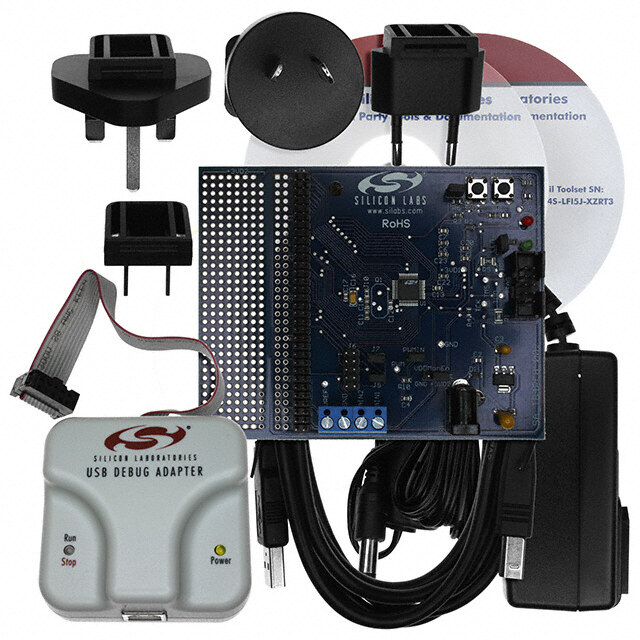
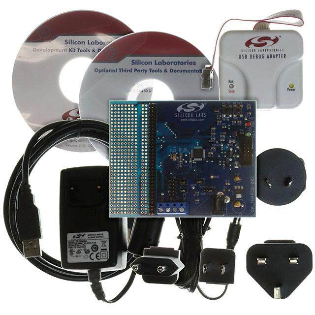
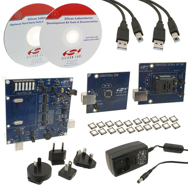
| 内容 | 板,电缆,LCD,电源 |
| 商标 | Altera Corporation |
| 商标名 | Stratix |
| 安装类型 | 固定 |
| 工作电源电压 | 19 V |
| 工具用于评估 | 5SGSMD5K2F40C2N |
| 平台 | - |
| 接口类型 | Ethernet, HSMC, JTAG, QSFP |
| 描述/功能 | Stratix V development kit |
| 操作系统 | - |
| 板类型 | 评估平台 |
| 标准包装 | 1 |
| 核心处理器 | - |
| 类型 | FPGA |
| 系列 | Stratix V |
| 配套使用产品/相关产品 | 5SGSMD5K2F40C2N |


- 商务部:美国ITC正式对集成电路等产品启动337调查
- 曝三星4nm工艺存在良率问题 高通将骁龙8 Gen1或转产台积电
- 太阳诱电将投资9.5亿元在常州建新厂生产MLCC 预计2023年完工
- 英特尔发布欧洲新工厂建设计划 深化IDM 2.0 战略
- 台积电先进制程称霸业界 有大客户加持明年业绩稳了
- 达到5530亿美元!SIA预计今年全球半导体销售额将创下新高
- 英特尔拟将自动驾驶子公司Mobileye上市 估值或超500亿美元
- 三星加码芯片和SET,合并消费电子和移动部门,撤换高东真等 CEO
- 三星电子宣布重大人事变动 还合并消费电子和移动部门
- 海关总署:前11个月进口集成电路产品价值2.52万亿元 增长14.8%

PDF Datasheet 数据手册内容提取
DSP Development Kit, StratixV Edition User Guide DSP Development Kit, Stratix V Edition User Guide 101 Innovation Drive San Jose, CA 95134 www.altera.com UG-01119-1.1 Feedback Subscribe
© 2013 Altera Corporation. All rights reserved. ALTERA, ARRIA, CYCLONE, HARDCOPY, MAX, MEGACORE, NIOS, QUARTUS and STRATIX words and logos are trademarks of Altera Corporation and registered in the U.S. Patent and Trademark Office and in other countries. All other words and logos identified as trademarks or service marks are the property of their respective holders as described at www.altera.com/common/legal.html. Altera warrants performance of its ISO semiconductor products to current specifications in accordance with Altera's standard warranty, but reserves the right to make changes to any products and 9001:2008 services at any time without notice. Altera assumes no responsibility or liability arising out of the application or use of any information, product, or service Registered described herein except as expressly agreed to in writing by Altera. Altera customers are advised to obtain the latest version of device specifications before relying on any published information and before placing orders for products or services. July 2013 Altera Corporation DSP Development Kit, StratixV Edition User Guide
Contents Chapter1. About This Kit Kit Features . . . . . . . . . . . . . . . . . . . . . . . . . . . . . . . . . . . . . . . . . . . . . . . . . . . . . . . . . . . . . . . . . . . . . . . . . . . . 1–1 Hardware . . . . . . . . . . . . . . . . . . . . . . . . . . . . . . . . . . . . . . . . . . . . . . . . . . . . . . . . . . . . . . . . . . . . . . . . . . . . 1–2 Software . . . . . . . . . . . . . . . . . . . . . . . . . . . . . . . . . . . . . . . . . . . . . . . . . . . . . . . . . . . . . . . . . . . . . . . . . . . . . 1–2 Quartus II Software . . . . . . . . . . . . . . . . . . . . . . . . . . . . . . . . . . . . . . . . . . . . . . . . . . . . . . . . . . . . . . . . . 1–2 The Development Kit Installer . . . . . . . . . . . . . . . . . . . . . . . . . . . . . . . . . . . . . . . . . . . . . . . . . . . . . . . . 1–3 Chapter2. Getting Started Before You Begin . . . . . . . . . . . . . . . . . . . . . . . . . . . . . . . . . . . . . . . . . . . . . . . . . . . . . . . . . . . . . . . . . . . . . . . . 2–1 Inspect the Board . . . . . . . . . . . . . . . . . . . . . . . . . . . . . . . . . . . . . . . . . . . . . . . . . . . . . . . . . . . . . . . . . . . . . 2–1 References . . . . . . . . . . . . . . . . . . . . . . . . . . . . . . . . . . . . . . . . . . . . . . . . . . . . . . . . . . . . . . . . . . . . . . . . . . . . . . 2–2 Chapter3. Software Installation Installing the Quartus II Subscription Edition Software . . . . . . . . . . . . . . . . . . . . . . . . . . . . . . . . . . . . . . . 3–1 Licensing Considerations . . . . . . . . . . . . . . . . . . . . . . . . . . . . . . . . . . . . . . . . . . . . . . . . . . . . . . . . . . . . . . 3–1 Installing the Development Kit . . . . . . . . . . . . . . . . . . . . . . . . . . . . . . . . . . . . . . . . . . . . . . . . . . . . . . . . . . . . 3–2 Installing the USB-Blaster II Driver . . . . . . . . . . . . . . . . . . . . . . . . . . . . . . . . . . . . . . . . . . . . . . . . . . . . . . . . 3–3 Chapter4. Development Board Setup Setting Up the Board . . . . . . . . . . . . . . . . . . . . . . . . . . . . . . . . . . . . . . . . . . . . . . . . . . . . . . . . . . . . . . . . . . . . . 4–1 Factory Default Switch Settings . . . . . . . . . . . . . . . . . . . . . . . . . . . . . . . . . . . . . . . . . . . . . . . . . . . . . . . . . . . 4–2 Chapter5. Board Update Portal Connecting to the Board Update Portal Web Page . . . . . . . . . . . . . . . . . . . . . . . . . . . . . . . . . . . . . . . . . . . 5–1 Using the Board Update Portal to Update User Designs . . . . . . . . . . . . . . . . . . . . . . . . . . . . . . . . . . . . . . 5–2 Chapter6. Board Test System Preparing the Board . . . . . . . . . . . . . . . . . . . . . . . . . . . . . . . . . . . . . . . . . . . . . . . . . . . . . . . . . . . . . . . . . . . . . 6–2 Running the Board Test System . . . . . . . . . . . . . . . . . . . . . . . . . . . . . . . . . . . . . . . . . . . . . . . . . . . . . . . . . . . 6–2 Using the Board Test System . . . . . . . . . . . . . . . . . . . . . . . . . . . . . . . . . . . . . . . . . . . . . . . . . . . . . . . . . . . . . . 6–3 The Configure Menu . . . . . . . . . . . . . . . . . . . . . . . . . . . . . . . . . . . . . . . . . . . . . . . . . . . . . . . . . . . . . . . . . . 6–3 The System Info Tab . . . . . . . . . . . . . . . . . . . . . . . . . . . . . . . . . . . . . . . . . . . . . . . . . . . . . . . . . . . . . . . . . . . 6–3 Board Information . . . . . . . . . . . . . . . . . . . . . . . . . . . . . . . . . . . . . . . . . . . . . . . . . . . . . . . . . . . . . . . . . . 6–3 MAXV Registers . . . . . . . . . . . . . . . . . . . . . . . . . . . . . . . . . . . . . . . . . . . . . . . . . . . . . . . . . . . . . . . . . . . 6–4 JTAG Chain . . . . . . . . . . . . . . . . . . . . . . . . . . . . . . . . . . . . . . . . . . . . . . . . . . . . . . . . . . . . . . . . . . . . . . . . 6–5 Flash Memory Map . . . . . . . . . . . . . . . . . . . . . . . . . . . . . . . . . . . . . . . . . . . . . . . . . . . . . . . . . . . . . . . . . 6–5 The GPIO Tab . . . . . . . . . . . . . . . . . . . . . . . . . . . . . . . . . . . . . . . . . . . . . . . . . . . . . . . . . . . . . . . . . . . . . . . . 6–6 Character LCD . . . . . . . . . . . . . . . . . . . . . . . . . . . . . . . . . . . . . . . . . . . . . . . . . . . . . . . . . . . . . . . . . . . . . 6–6 User DIP Switches . . . . . . . . . . . . . . . . . . . . . . . . . . . . . . . . . . . . . . . . . . . . . . . . . . . . . . . . . . . . . . . . . . 6–6 User LEDs . . . . . . . . . . . . . . . . . . . . . . . . . . . . . . . . . . . . . . . . . . . . . . . . . . . . . . . . . . . . . . . . . . . . . . . . . 6–7 Push Button Switches . . . . . . . . . . . . . . . . . . . . . . . . . . . . . . . . . . . . . . . . . . . . . . . . . . . . . . . . . . . . . . . 6–7 The Flash Tab . . . . . . . . . . . . . . . . . . . . . . . . . . . . . . . . . . . . . . . . . . . . . . . . . . . . . . . . . . . . . . . . . . . . . . . . 6–7 Read . . . . . . . . . . . . . . . . . . . . . . . . . . . . . . . . . . . . . . . . . . . . . . . . . . . . . . . . . . . . . . . . . . . . . . . . . . . . . . 6–8 Write . . . . . . . . . . . . . . . . . . . . . . . . . . . . . . . . . . . . . . . . . . . . . . . . . . . . . . . . . . . . . . . . . . . . . . . . . . . . . 6–8 Random Test . . . . . . . . . . . . . . . . . . . . . . . . . . . . . . . . . . . . . . . . . . . . . . . . . . . . . . . . . . . . . . . . . . . . . . . 6–8 CFI Query . . . . . . . . . . . . . . . . . . . . . . . . . . . . . . . . . . . . . . . . . . . . . . . . . . . . . . . . . . . . . . . . . . . . . . . . . 6–8 Increment Test . . . . . . . . . . . . . . . . . . . . . . . . . . . . . . . . . . . . . . . . . . . . . . . . . . . . . . . . . . . . . . . . . . . . . 6–8 Reset . . . . . . . . . . . . . . . . . . . . . . . . . . . . . . . . . . . . . . . . . . . . . . . . . . . . . . . . . . . . . . . . . . . . . . . . . . . . . . 6–8 July 2013 Altera Corporation DSP Development Kit, StratixV Edition User Guide
iv Contents Erase . . . . . . . . . . . . . . . . . . . . . . . . . . . . . . . . . . . . . . . . . . . . . . . . . . . . . . . . . . . . . . . . . . . . . . . . . . . . . . 6–8 Flash Memory Map . . . . . . . . . . . . . . . . . . . . . . . . . . . . . . . . . . . . . . . . . . . . . . . . . . . . . . . . . . . . . . . . . 6–8 The DDR3 Tab . . . . . . . . . . . . . . . . . . . . . . . . . . . . . . . . . . . . . . . . . . . . . . . . . . . . . . . . . . . . . . . . . . . . . . . . 6–9 Start . . . . . . . . . . . . . . . . . . . . . . . . . . . . . . . . . . . . . . . . . . . . . . . . . . . . . . . . . . . . . . . . . . . . . . . . . . . . . . 6–9 Stop . . . . . . . . . . . . . . . . . . . . . . . . . . . . . . . . . . . . . . . . . . . . . . . . . . . . . . . . . . . . . . . . . . . . . . . . . . . . . . 6–9 Performance Indicators . . . . . . . . . . . . . . . . . . . . . . . . . . . . . . . . . . . . . . . . . . . . . . . . . . . . . . . . . . . . . . 6–9 Error Control . . . . . . . . . . . . . . . . . . . . . . . . . . . . . . . . . . . . . . . . . . . . . . . . . . . . . . . . . . . . . . . . . . . . . 6–10 Number of Addresses to Write and Read . . . . . . . . . . . . . . . . . . . . . . . . . . . . . . . . . . . . . . . . . . . . . 6–10 Data Type . . . . . . . . . . . . . . . . . . . . . . . . . . . . . . . . . . . . . . . . . . . . . . . . . . . . . . . . . . . . . . . . . . . . . . . . 6–10 Read and Write Control . . . . . . . . . . . . . . . . . . . . . . . . . . . . . . . . . . . . . . . . . . . . . . . . . . . . . . . . . . . . 6–10 The QDRII+ Tab . . . . . . . . . . . . . . . . . . . . . . . . . . . . . . . . . . . . . . . . . . . . . . . . . . . . . . . . . . . . . . . . . . . . . 6–11 Start . . . . . . . . . . . . . . . . . . . . . . . . . . . . . . . . . . . . . . . . . . . . . . . . . . . . . . . . . . . . . . . . . . . . . . . . . . . . . 6–11 Stop . . . . . . . . . . . . . . . . . . . . . . . . . . . . . . . . . . . . . . . . . . . . . . . . . . . . . . . . . . . . . . . . . . . . . . . . . . . . . 6–11 Performance Indicators . . . . . . . . . . . . . . . . . . . . . . . . . . . . . . . . . . . . . . . . . . . . . . . . . . . . . . . . . . . . . 6–12 Error Control . . . . . . . . . . . . . . . . . . . . . . . . . . . . . . . . . . . . . . . . . . . . . . . . . . . . . . . . . . . . . . . . . . . . . 6–12 Number of Addresses to Write and Read . . . . . . . . . . . . . . . . . . . . . . . . . . . . . . . . . . . . . . . . . . . . . 6–12 Data Type . . . . . . . . . . . . . . . . . . . . . . . . . . . . . . . . . . . . . . . . . . . . . . . . . . . . . . . . . . . . . . . . . . . . . . . . 6–12 The XCVR1 Tab . . . . . . . . . . . . . . . . . . . . . . . . . . . . . . . . . . . . . . . . . . . . . . . . . . . . . . . . . . . . . . . . . . . . . . 6–13 Status . . . . . . . . . . . . . . . . . . . . . . . . . . . . . . . . . . . . . . . . . . . . . . . . . . . . . . . . . . . . . . . . . . . . . . . . . . . . 6–13 Port . . . . . . . . . . . . . . . . . . . . . . . . . . . . . . . . . . . . . . . . . . . . . . . . . . . . . . . . . . . . . . . . . . . . . . . . . . . . . . 6–14 PMA Setting . . . . . . . . . . . . . . . . . . . . . . . . . . . . . . . . . . . . . . . . . . . . . . . . . . . . . . . . . . . . . . . . . . . . . . 6–14 Data Type . . . . . . . . . . . . . . . . . . . . . . . . . . . . . . . . . . . . . . . . . . . . . . . . . . . . . . . . . . . . . . . . . . . . . . . . 6–14 Error Control . . . . . . . . . . . . . . . . . . . . . . . . . . . . . . . . . . . . . . . . . . . . . . . . . . . . . . . . . . . . . . . . . . . . . 6–15 Start . . . . . . . . . . . . . . . . . . . . . . . . . . . . . . . . . . . . . . . . . . . . . . . . . . . . . . . . . . . . . . . . . . . . . . . . . . . . . 6–15 Stop . . . . . . . . . . . . . . . . . . . . . . . . . . . . . . . . . . . . . . . . . . . . . . . . . . . . . . . . . . . . . . . . . . . . . . . . . . . . . 6–15 Performance Indicators . . . . . . . . . . . . . . . . . . . . . . . . . . . . . . . . . . . . . . . . . . . . . . . . . . . . . . . . . . . . . 6–15 The XCVR2 Tab . . . . . . . . . . . . . . . . . . . . . . . . . . . . . . . . . . . . . . . . . . . . . . . . . . . . . . . . . . . . . . . . . . . . . . 6–16 Status . . . . . . . . . . . . . . . . . . . . . . . . . . . . . . . . . . . . . . . . . . . . . . . . . . . . . . . . . . . . . . . . . . . . . . . . . . . . 6–16 Port . . . . . . . . . . . . . . . . . . . . . . . . . . . . . . . . . . . . . . . . . . . . . . . . . . . . . . . . . . . . . . . . . . . . . . . . . . . . . . 6–17 PMA Setting . . . . . . . . . . . . . . . . . . . . . . . . . . . . . . . . . . . . . . . . . . . . . . . . . . . . . . . . . . . . . . . . . . . . . . 6–17 Data Type . . . . . . . . . . . . . . . . . . . . . . . . . . . . . . . . . . . . . . . . . . . . . . . . . . . . . . . . . . . . . . . . . . . . . . . . 6–17 Error Control . . . . . . . . . . . . . . . . . . . . . . . . . . . . . . . . . . . . . . . . . . . . . . . . . . . . . . . . . . . . . . . . . . . . . 6–18 Start . . . . . . . . . . . . . . . . . . . . . . . . . . . . . . . . . . . . . . . . . . . . . . . . . . . . . . . . . . . . . . . . . . . . . . . . . . . . . 6–18 Stop . . . . . . . . . . . . . . . . . . . . . . . . . . . . . . . . . . . . . . . . . . . . . . . . . . . . . . . . . . . . . . . . . . . . . . . . . . . . . 6–18 Performance Indicators . . . . . . . . . . . . . . . . . . . . . . . . . . . . . . . . . . . . . . . . . . . . . . . . . . . . . . . . . . . . . 6–18 The XCVR3 Tab . . . . . . . . . . . . . . . . . . . . . . . . . . . . . . . . . . . . . . . . . . . . . . . . . . . . . . . . . . . . . . . . . . . . . . 6–19 Status . . . . . . . . . . . . . . . . . . . . . . . . . . . . . . . . . . . . . . . . . . . . . . . . . . . . . . . . . . . . . . . . . . . . . . . . . . . . 6–19 Port . . . . . . . . . . . . . . . . . . . . . . . . . . . . . . . . . . . . . . . . . . . . . . . . . . . . . . . . . . . . . . . . . . . . . . . . . . . . . . 6–20 PMA Setting . . . . . . . . . . . . . . . . . . . . . . . . . . . . . . . . . . . . . . . . . . . . . . . . . . . . . . . . . . . . . . . . . . . . . . 6–20 Data Type . . . . . . . . . . . . . . . . . . . . . . . . . . . . . . . . . . . . . . . . . . . . . . . . . . . . . . . . . . . . . . . . . . . . . . . . 6–20 Error Control . . . . . . . . . . . . . . . . . . . . . . . . . . . . . . . . . . . . . . . . . . . . . . . . . . . . . . . . . . . . . . . . . . . . . 6–21 Start . . . . . . . . . . . . . . . . . . . . . . . . . . . . . . . . . . . . . . . . . . . . . . . . . . . . . . . . . . . . . . . . . . . . . . . . . . . . . 6–21 Stop . . . . . . . . . . . . . . . . . . . . . . . . . . . . . . . . . . . . . . . . . . . . . . . . . . . . . . . . . . . . . . . . . . . . . . . . . . . . . 6–21 Performance Indicators . . . . . . . . . . . . . . . . . . . . . . . . . . . . . . . . . . . . . . . . . . . . . . . . . . . . . . . . . . . . . 6–21 The Power Monitor . . . . . . . . . . . . . . . . . . . . . . . . . . . . . . . . . . . . . . . . . . . . . . . . . . . . . . . . . . . . . . . . . . . . . 6–21 General Information . . . . . . . . . . . . . . . . . . . . . . . . . . . . . . . . . . . . . . . . . . . . . . . . . . . . . . . . . . . . . . . 6–22 Temperature Information . . . . . . . . . . . . . . . . . . . . . . . . . . . . . . . . . . . . . . . . . . . . . . . . . . . . . . . . . . . 6–23 Power Information . . . . . . . . . . . . . . . . . . . . . . . . . . . . . . . . . . . . . . . . . . . . . . . . . . . . . . . . . . . . . . . . . 6–23 Power Graph . . . . . . . . . . . . . . . . . . . . . . . . . . . . . . . . . . . . . . . . . . . . . . . . . . . . . . . . . . . . . . . . . . . . . 6–23 Graph Settings . . . . . . . . . . . . . . . . . . . . . . . . . . . . . . . . . . . . . . . . . . . . . . . . . . . . . . . . . . . . . . . . . . . . 6–23 Reset . . . . . . . . . . . . . . . . . . . . . . . . . . . . . . . . . . . . . . . . . . . . . . . . . . . . . . . . . . . . . . . . . . . . . . . . . . . . . 6–23 The Clock Control . . . . . . . . . . . . . . . . . . . . . . . . . . . . . . . . . . . . . . . . . . . . . . . . . . . . . . . . . . . . . . . . . . . . . . 6–23 Read . . . . . . . . . . . . . . . . . . . . . . . . . . . . . . . . . . . . . . . . . . . . . . . . . . . . . . . . . . . . . . . . . . . . . . . . . . . . . 6–24 Default . . . . . . . . . . . . . . . . . . . . . . . . . . . . . . . . . . . . . . . . . . . . . . . . . . . . . . . . . . . . . . . . . . . . . . . . . . . 6–25 DSP Development Kit, StratixV Edition July 2013 Altera Corporation User Guide
Contents v Set New Frequency . . . . . . . . . . . . . . . . . . . . . . . . . . . . . . . . . . . . . . . . . . . . . . . . . . . . . . . . . . . . . . . . 6–25 Configuring the FPGA Using the QuartusII Programmer . . . . . . . . . . . . . . . . . . . . . . . . . . . . . . . . . . . . 6–25 AppendixA. Programming the Flash Memory Device CFI Flash Memory Map . . . . . . . . . . . . . . . . . . . . . . . . . . . . . . . . . . . . . . . . . . . . . . . . . . . . . . . . . . . . . . . . . A–1 Preparing Design Files for Flash Programming . . . . . . . . . . . . . . . . . . . . . . . . . . . . . . . . . . . . . . . . . . . . . A–2 Creating Flash Files Using the NiosII EDS . . . . . . . . . . . . . . . . . . . . . . . . . . . . . . . . . . . . . . . . . . . . . . A–2 Programming Flash Memory Using the Board Update Portal . . . . . . . . . . . . . . . . . . . . . . . . . . . . . . . . . A–3 Programming Flash Memory Using the NiosII EDS . . . . . . . . . . . . . . . . . . . . . . . . . . . . . . . . . . . . . . . . . A–3 Restoring the Flash Device to the Factory Settings . . . . . . . . . . . . . . . . . . . . . . . . . . . . . . . . . . . . . . . . . . A–4 Restoring the MAXV CPLD to the Factory Settings . . . . . . . . . . . . . . . . . . . . . . . . . . . . . . . . . . . . . . . . . A–5 Additional Information Document Revision History . . . . . . . . . . . . . . . . . . . . . . . . . . . . . . . . . . . . . . . . . . . . . . . . . . . . . . . . . . . Info–1 How to Contact Altera . . . . . . . . . . . . . . . . . . . . . . . . . . . . . . . . . . . . . . . . . . . . . . . . . . . . . . . . . . . . . . . . Info–1 Typographic Conventions . . . . . . . . . . . . . . . . . . . . . . . . . . . . . . . . . . . . . . . . . . . . . . . . . . . . . . . . . . . . . Info–1 July 2013 Altera Corporation DSP Development Kit, StratixV Edition User Guide
vi Contents DSP Development Kit, StratixV Edition July 2013 Altera Corporation User Guide
1. About This Kit The Altera® DSP Development Kit,Stratix®V Edition, is a complete design environment that includes both the hardware and software you need to develop StratixVGS FPGA designs. The following list describes what you can accomplish with the kit: ■ Test Altera's optimized variable-precision digital signal processing (DSP) block (part of the Stratix V FPGA architecture), which supports various datapath precisions ranging from 9-bit x 9-bit up to single-precision floating point within a single block (while maintaining performance and low power). ■ Develop DSP algorithms in a high-level model-based flow using Altera's DSP Builder Advanced Blockset with MathWorks' MATLAB & Simulink tools. 1 For more information on the DSP-specific aspects of this board, refer to “References” on page2–2. ■ Test signal quality of the FPGA transceiver I/Os (10 Gbps+). ■ Develop and test PCI Express® (PCIe) 3.0 designs. ■ Develop and test memory subsystems consisting of SyncFlash, DDR3, and QDRII+. ■ Develop and test SDI with the embedded 75-ohm 3G SDI transceivers. ■ Develop embedded designs utilizing the Nios®II processor and external memory. ■ Develop and test network designs utilizing Triple Speed Ethernet MegaCore® and external RJ-45 jack. ■ Develop and test optical networking designs using the 10-Gbps and 40-Gbps Ethernet MAC MegaCores and the QSFP Optical Interface. ■ Take advantage of the modular and scalable design by using the high-speed mezzanine card (HSMC) connectors to interface to over 40 different HSMCs provided by Altera partners, supporting protocols such as Serial RapidIO®, 10Gigabit Ethernet, SONET, Common Public Radio Interface (CPRI), Open Base Station Architecture Initiative (OBSAI) and others. ■ Measure the FPGA's power consumption. ■ Control twelve different programmable clock oscillators using the Clock Control GUI. Kit Features This section briefly describes the DSP Development Kit, StratixV Edition, contents. July 2013 Altera Corporation DSP Development Kit, StratixV Edition User Guide
1–2 Chapter 1: About This Kit Kit Features Hardware The DSP Development Kit, StratixV Edition, includes the following hardware: ■ StratixVGS development board—A development platform that allows you to develop and prototype hardware designs running on the StratixVGS 5SGSMD5K2F40C2N device. f For detailed information about the board components and interfaces, refer to the DSP Development Kit, StratixV EditionReference Manual. ■ HSMC loopback board—A daughtercard that allows for loopback testing all signals on the HSMC interface using the Board Test System. ■ Power supply and cables—The kit includes the following items: ■ Power supply and AC adapters for North America/Japan, Europe, and the United Kingdom ■ Standard USB A to micro-USB cable ■ Ethernet cable ■ 75Ω SMB video cable Software The software for this kit, described in the following sections, is available on the Altera website for immediate downloading. You can also request to have Altera mail the software to you on DVDs. Quartus II Software Your kit includes a license for the Development Kit Edition (DKE) of the Quartus II software (Windows platform only). For one year, this license entitles you to most of the features of the Subscription Edition (excluding the IP Base Suite). 1 After the year, your DKE license will no longer be valid and you will not be permitted to use this version of the Quartus II software. To continue using the Quartus II software, you should download the free Quartus II Web Edition or purchase a subscription to Quartus II software. For more information, refer to the Design Software page of the Altera website. The Quartus II Development Kit Edition (DKE) software includes the following items: ■ QuartusII Software—The QuartusII software, including the Qsys system integration tool, provides a comprehensive environment for network on a chip (NoC) design. The QuartusII software integrates into nearly any design environment and provides interfaces to industry-standard EDA tools. DSP Development Kit, StratixV Edition July 2013 Altera Corporation User Guide
Chapter 1: About This Kit 1–3 Kit Features ■ MegaCore® IP Library—A library that contains Altera IP MegaCore functions. You can evaluate MegaCore functions by using the OpenCore Plus feature to do the following: ■ Simulate behavior of a MegaCore function within your system. ■ Verify functionality of your design, and quickly and easily evaluate its size and speed. ■ Generate time-limited device programming files for designs that include MegaCore functions. ■ Program a device and verify your design in hardware. 1 The OpenCore Plus hardware evaluation feature is an evaluation tool for prototyping only. You must purchase a license to use a MegaCore function in production. f For more information about OpenCore Plus, refer to AN 320: OpenCore Plus Evaluation of Megafunctions. ■ Nios®II Embedded Design Suite (EDS)—A full-featured set of tools that allows you to develop embedded software for the NiosII processor that you can include in your Altera FPGA designs. The Development Kit Installer The license-free DSP Development Kit, StratixV Edition, installer includes all the documentation and design examples for the kit. For information on installing the Development Kit Installer, refer to “Software Installation” on page3–1. July 2013 Altera Corporation DSP Development Kit, StratixV Edition User Guide
1–4 Chapter 1: About This Kit Kit Features DSP Development Kit, StratixV Edition July 2013 Altera Corporation User Guide
2. Getting Started The remaining chapters in this user guide lead you through the following StratixVGS development board setup steps: ■ Inspecting the contents of the kit ■ Installing the design and kit software ■ Setting up, powering up, and verifying correct operation of the development board ■ Configuring the StratixVGS FPGA ■ Running the Board Test System designs f For complete information about the development board, refer to the DSP Development Kit, StratixV EditionReference Manual. Before You Begin Before using the kit or installing the software, check the kit contents and inspect the board to verify that you received all of the items listed in “Kit Features” on page1–1. If any of the items are missing, contact Altera before you proceed. Inspect the Board To inspect the board, perform the following steps: 1. Place the board on an anti-static surface and inspect it to ensure that it has not been damaged during shipment. c Without proper anti-static handling, you can damage the board. 2. Verify that all components are on the board and appear intact. 1 In typical applications with the StratixVGS development board, a heat sink is not necessary. However, under extreme conditions or for engineering sample silicon the board might require additional cooling to stay within operating temperature guidelines. The board has two holes near the FPGA that accommodate many different heat sinks, including the Dynatron CHR-152. You can perform power consumption and thermal modeling to determine whether your application requires additional cooling. For information about measuring board and FPGA temperature in real time, refer to “The Power Monitor” on page6–21. f For more information about power consumption and thermal modeling, refer to AN358: Thermal Management for FPGAs. July 2013 Altera Corporation DSP Development Kit, StratixV Edition User Guide
2–2 Chapter 2: Getting Started References References Use the following links to check the Altera website for other related information: ■ To learn how Altera FPGAs have overcome traditional FPGA floating-point challenges, refer to the An independent Analysis of Altera's FPGA Floating-point DSP Design Flow white paper by the staff of Berkeley Design Technology, Inc. ■ To learn how it is possible to achieve one teraFLOPS performance with Stratix V devices, refer to the Achieving One TeraFLOPS with 28-nm FPGAs white paper. ■ For information on the DSP Builder, refer to the DSP Builder page. ■ For a free trial of the MATLAB & Simulink for use with DSP Builder, refer to the MathWorks website (www.mathworks.com). ■ For DSP Builder design examples, refer to the DSP Designs Examples page. ■ For the latest board design files and reference designs, refer to the DSP Development Kit, StratixV Edition page. ■ For additional daughter cards available for purchase, refer to the Development Board Daughtercards page. ■ For the StratixVGS device documentation, refer to the Documentation: Stratix V Devices page. ■ To purchase devices from the eStore, refer to the Devices page. ■ For StratixVGS OrCAD symbols, refer to the Capture CIS Symbols page. ■ For NiosII 32-bit embedded processor solutions, refer to the Embedded Processing page. DSP Development Kit, StratixV Edition July 2013 Altera Corporation User Guide
3. Software Installation This chapter explains how to install the following software: ■ Quartus II Subscription Edition Software ■ DSP Development Kit, StratixV Edition ■ USB-Blaster™ II driver Installing the Quartus II Subscription Edition Software Included in the QuartusII Subscription Edition Software are the QuartusII software (including Qsys), the NiosII EDS, and the MegaCore IP Library. To install the Altera development tools, perform the following steps: 1. Download the QuartusII Subscription Edition Software from the QuartusII Subscription Edition Software page of the Altera website. Alternatively, you can request a DVD from the Altera IP and Software DVD Request Form page of the Altera website. 2. Follow the on-screen instructions to complete the installation process. f If you have difficulty installing the QuartusII software, refer to the Altera Software Installation and Licensing Manual. Licensing Considerations Purchasing this kit entitles you to a one-year license for the Development Kit Edition (DKE) of the QuartusII software. 1 After the year, your DKE license will no longer be valid and you will not be permitted to use this version of the Quartus II software. To continue using the Quartus II software, you should download the free Quartus II Web Edition or purchase a subscription to Quartus II software. Before using the QuartusII software, you must activate your license, identify specific users and computers, and obtain and install a license file. If you already have a licensed version of the subscription edition, you can use that license file with this kit. If not, you need to obtain and install a license file. To begin, go to the Self Service Licensing Center page of the Altera website, log into or create your myAltera account, and take the following actions: 1. On the Activate Products page, enter the serial number provided with your development kit in the License Activation Code box. 1 Your serial number is printed on the side of the development kit box below the bottom bar code. The number is consists of alphanumeric characters, such as 5SDSPxxxxxxxxx, and does not contain hyphens. July 2013 Altera Corporation DSP Development Kit, StratixV Edition User Guide
3–2 Chapter 3: Software Installation Installing the Development Kit 2. Consult the Activate Products table, to determine how to proceed. a. If the administrator listed for your product is someone other than you, skip the remaining steps and contact your administrator to become a licensed user. b. If the administrator listed for your product is you, proceed to step 3. c. If the administrator listed for your product is Stocking, activate the product, making you the administrator, and proceed to step 3. 3. Use the Create New License page to license your product for a specific user (you) on specific computers. The Manage Computers and Manage Users pages allow you to add users and computers not already present in the licensing system. 1 To license the QuartusII software, you need your computer’s network interface card (NIC) ID, a number that uniquely identifies your computer. On the computer you use to run the QuartusII software, type ipconfig /all at a command prompt to determine the NIC ID. Your NIC ID is the 12-digit hexadecimal number on the Physical Address line. 4. When licensing is complete, Altera emails a license.dat file to you. Store the file on your computer and use the License Setup page of the Options dialog box in the Quartus_II software to enable the software. f For complete licensing details, refer to the Altera Software Installation and Licensing Manual. Installing the Development Kit To install the DSP Development Kit, StratixV Edition, perform the following steps: 1. Download the DSP Development Kit, StratixV Edition, installer from the DSP Development Kit, StratixV Edition page of the Altera website. Alternatively, you can request a development kit DVD from the Altera Kit Installations DVD Request Form page of the Altera website. 2. Run the DSP Development Kit, StratixV Edition, installer. 3. Follow the on-screen instructions to complete the installation process. Be sure that the installation directory you choose is in the same relative location to the QuartusII software installation. DSP Development Kit, StratixV Edition July 2013 Altera Corporation User Guide
Chapter 3: Software Installation 3–3 Installing the USB-Blaster II Driver The installation program creates the DSP Development Kit, StratixV Edition, directory structure shown in Figure3–1. Figure3–1. DSP Development Kit, StratixV Edition Installed Directory Structure (1) <install dir> The default Windows installation directory is C:\altera\<version>\. kits stratixVGS_5sgsmd5kf40_dsp board_design_files demos documents examples factory_recovery Note to Figure3–1: (1) Early-release versions might have slightly different directory names. Table3–1 lists the file directory names and a description of their contents. Table3–1. Installed Directory Contents Directory Name Description of Contents Contains schematic, layout, assembly, and bill of material board design files. Use these files as a board_design_files starting point for a new prototype board design. demos Contains demonstration applications when available. documents Contains the kit documentation. examples Contains the sample design files for the DSP Development Kit, StratixV Edition. Contains the original data programmed onto the board before shipment. Use this data to restore factory_recovery the board with its original factory contents. Installing the USB-Blaster II Driver The StratixVGS development board includes integrated On-Board USB-Blaster II circuitry for FPGA programming. However, for the host computer and board to communicate, you must install the USB-Blaster II driver on the host computer. f Installation instructions for the USB-Blaster II driver for your operating system are available on the Altera website. On the Altera Programming Cable Driver Information page of the Altera website, locate the table entry for your configuration and click the link to access the instructions. f For USB-Blaster II configuration details, refer to the On-Board USB-Blaster II page. July 2013 Altera Corporation DSP Development Kit, StratixV Edition User Guide
3–4 Chapter 3: Software Installation Installing the USB-Blaster II Driver DSP Development Kit, StratixV Edition July 2013 Altera Corporation User Guide
4. Development Board Setup The instructions in this chapter explain how to set up the StratixVGS development board. Setting Up the Board To prepare and apply power to the board, perform the following steps: 1. The StratixVGS development board ships with its board switches preconfigured to support the design examples in the kit. If you suspect your board might not be currently configured with the default settings, follow the instructions in “Factory Default Switch Settings” on page4–2 to return the board to its factory settings before proceeding. 2. The development board ships with design examples stored in the flash memory device. Verify the DIP switch SW5.3 is set to the off position to load the design stored in the factory portion of flash memory. Figure4–2 shows the DIP switch location on the back of the StratixVGS development board. 3. Verify that the HSMC card is installed on port A (connector J1) of the board. 4. Verify that the HSMC card is installed on port B (connector J2) of the board. 5. Ensure that the power switch SW2 is in the off position. 6. Connect the Power Adpater +19 V, 6.32 A to the DC Power Jack (J4) on the FPGA board and plug the cord into a power outlet. c Use only the supplied power supply. Power regulation circuitry on the board can be damaged by power supplies with greater voltage. 7. Set the POWER switch (SW2) to the on position. When power is supplied to the board, Power blue LED (D24) illuminates indicating that the board has power. The MAXV device on the board contains (among other things) a parallel flash loader (PFL) megafunction. When the board powers up, the PFL reads a design from flash memory and configures the FPGA. The DIP switch SW5.3 controls which design to load. When the switch is in the off position, the PFL loads the design from the factory portion of flash memory. 1 The kit includes a MAXV design which contains the MAXV PFL megafunction. The design resides in the <install dir>\kits\stratixVGS_5sgsmd5kf40_dsp\examples\max5 directory. When configuration is complete, the Config Done LED (D17) illuminates, signaling that the StratixVGS device configured successfully. f For more information about the PFL megafunction, refer to AN 386: Parallel Flash Loader Megafunction User Guide. July 2013 Altera Corporation DSP Development Kit, StratixV Edition User Guide
4–2 Chapter 4: Development Board Setup Factory Default Switch Settings Factory Default Switch Settings This section shows the factory switch settings for the StratixVGS development board. Figure4–1 shows the switch locations and the default position of each switch on the top side of the board. Figure4–1. Switch Locations and Default Settings on the Board Top SW1 87654321 OFF = 1 ON = 0 ON User DIP Switch Default: no jumper installed for 2.5 V VCCIO J8 2.5 V 1.8 V 1.5 V HSMB VCCIO DSP Development Kit, StratixV Edition July 2013 Altera Corporation User Guide
Chapter 4: Development Board Setup 4–3 Factory Default Switch Settings Figure4–2 shows the switch locations and the default position of each switch on the bottom side of the board. Figure4–2. Switch Locations and Default Settings on the Board Bottom AXVSMASMBCIE MHHP SW3 ON ON SW4 ON = 0 OFF = 1 1 2 3 4 1 2 3 4 5 6 JTAG MSEL CURITYCTORYK_ENK_SEL SEFACLCL SW6 4 3 2 1 ON ON = 0 OFF = 1 ON 1 2 3 4 SW5 x1 x4 x8 To restore the switches to their factory default settings, perform the following steps: 1. Set jumper block (J8) to match Table4–1 and Figure4–1. Table4–1. J8 Jumper Block (1) Jumper HSMB VCCIO Position Pins 1-2 1.8 V Not installed Pins 3-4 1.5 V Not installed Pins 5-6 1.2 V Not installed No pins 2.5 V Default Note to Table4–1: (1) Adding a single jumper between the pins sets the voltage as described in the table. Install only one jumper location at a time. July 2013 Altera Corporation DSP Development Kit, StratixV Edition User Guide
4–4 Chapter 4: Development Board Setup Factory Default Switch Settings 2. Set the DIP switch bank (SW3) to match Table4–2 and Figure4–2. Table4–2. SW3 JTAG DIP Switch Settings (1) Switc Board Default Function h Label Position Switch 1 has the following options: ■ When on (0), removes the MAX V system controller in 1 MAX_JTAG_EN the JTAG chain. Off ■ When off (1), includes the MAX V system controller from the JTAG chain. Switch 2 has the following options: ■ When on (0), removes the HSMC Port A in the JTAG 2 HSMA_JTAG_EN chain. On ■ When off (1), includes the HSMC Port A from the JTAG chain. Switch 3 has the following options: ■ When on (0), removes the HSMC Port B in the JTAG 3 HSMB_JTAG_EN chain. On ■ When off (1), includes the HSMC Port B from the JTAG chain. Switch 4 has the following options: ■ When on (0), removes the PCI Express Edge connector 4 PCIE_JTAG_EN from the JTAG chain. On ■ When off (1), includes the PCI Express Edge connector in the JTAG chain. Note to Table4–2: (1) If you plug in an external USB-Blaster cable to the JTAG header (J10), the On Board USB-Blaster II is disabled. The JTAG chain is normally mastered by the on-board USB-Blaster II. f For details on the JTAG chain, refer to the DSP Development Kit, StratixV EditionReference Manual. For USB-Blaster II configuration details, refer to the On-Board USB-Blaster II page. 3. Set DIP switch bank (SW4) to match Table4–3 and Figure4–2. Table4–3. SW4 MSEL DIP Switch Settings (1) Board Default Switch Function Label Position 1 MSEL0 Configuration Setting 0 On (0) 2 MSEL1 Configuration Setting 1 On (0) 3 MSEL2 Configuration Setting 2 On (0) 4 MSEL3 Configuration Setting 3 Off (1) 5 MSEL4 Configuration Setting 4 On (0) 6 — — On (0) Note to: Table4–3 (1) Set MSEL[4:0] to valid configuration schemes as listed in the Stratix V Device Handbook. DSP Development Kit, StratixV Edition July 2013 Altera Corporation User Guide
Chapter 4: Development Board Setup 4–5 Factory Default Switch Settings f For more information, refer to the Configuration Schemes section in volume 2, Chapter 9, of the Stratix V Device Handbook. 4. Set DIP switch bank (SW5) to match Table4–4 and Figure4–2. 1 If you use an external USB Blaster, Altera recommends that you disable the power-up configuration of the FPGA by changing the MSEL(4:0) DIP switch (SW4) from 01000 to 11000. This will prevent power-up FPGA configuration from flash in the default FPPx32 mode. The On-Board USB-Blaster II is disabled when you plug in an external USB Blaster, which prevents the JTAG FACTORY command from being sent to disable the security mode JTAG lockout prior to configuring the Stratix V. The On-Board USB-Blaster II issues the JTAG FACTORY command when the SECURITY switch (SW5.4) is set to 1. For more information on the Stratix V ES JTAG Port Access Limitation After Configuration, refer to the Errata Sheet and Guidelines for Stratix V ES Devices. Table4–4. SW5 DIP Switch Settings Switc Board Default Function h Label Position Switch 1 has the following options: ■ When on (0), the SMA input clock is selected. 1 CLK_SEL Off ■ When off (1), the programmable oscillator clock is selected. Switch 2 has the following options: 2 CLK_EN (1) ■ When on (0), the on-board oscillator is enabled. On ■ When off (1), the on-board oscillator is disabled. Switch 3 has the following options: ■ When on (0), loads the user design from flash at power 3 FACTORY (1) up. Off ■ When off (1), loads the factory design from flash at power up. Switch 4 has the following options: ■ When on (0), does not send factory command at power 4 SECURITY (1) Off up. ■ When off (1), sends factory command at power up. Note to Table4–4: (1) Functionality of the CLK_EN, FACTORY and SECURITY settings are dependent on the MAX V system controller CPLD. In order to function properly, the MAX V CPLD must be programmed with the required MAX V design. July 2013 Altera Corporation DSP Development Kit, StratixV Edition User Guide
4–6 Chapter 4: Development Board Setup Factory Default Switch Settings 5. Set DIP switch bank (SW6) to match Table4–5 and Figure4–2. Table4–5. SW6 DIP Switch Settings Switc Board Default Function h Label Position Switch 1 has the following options: PCIE_PRSNT2 1 ■ When on (0), x1 presence detect is enabled. On n_x1 ■ When off (1), x1 presence detect is disabled. Switch 2 has the following options: PCIE_PRSNT2 2 ■ When on (0), x4 presence detect is enabled. On n_x4 ■ When off (1), x4 presence detect is disabled. Switch 3 has the following options: PCIE_PRSNT2 3 ■ When on (0), x8 presence detect is enabled. On n_x8 ■ When off (1), x8 presence detect is disabled. 4 — — Off f For more information about the FPGA board settings, refer to the DSP Development Kit, StratixV EditionReference Manual. DSP Development Kit, StratixV Edition July 2013 Altera Corporation User Guide
5. Board Update Portal The DSP Development Kit, StratixV Edition, ships with the Board Update Portal design example stored in the factory portion of the flash memory on the board. The design consists of a NiosII embedded processor, an Ethernet MAC, and an HTML web server. When you power up the board with the DIP switch SW5.3 in the off position, the StratixVGS FPGA configures with the Board Update Portal design example. The design can obtain an IP address from any DHCP server and serve a web page from the flash on your board to any host computer on the same network. The web page allows you to upload new FPGA designs to the user hardware 1 portion of flash memory and provides useful kit-specific links and design resources. 1 After successfully updating the user hardware 1 flash memory, you can load the design from flash memory into the FPGA. To do so, set the DIP switch SW5.3 to the on position and power cycle the board, which loads the user 1 design into flash. The source code for the Board Update Portal design resides in the <install dir>\kits\stratixVGS_5sgsmd5kf40_dsp\examples directory. If the Board Update Portal is corrupted or deleted from the flash memory, refer to “Restoring the Flash Device to the Factory Settings” on pageA–4 to restore the board with its original factory contents. Connecting to the Board Update Portal Web Page This section provides instructions to connect to the Board Update Portal web page. 1 Before you proceed, ensure that you have the following: ■ A PC with a connection to a working Ethernet port on a DHCP enabled network. ■ A separate working Ethernet port connected to the same network for the board. ■ The Ethernet and power cables that are included in the kit. To connect to the Board Update Portal web page, perform these steps: 1. With the board powered down, set the DIP switch SW5.3 to the off position, which loads the factory design into flash. 2. Attach the Ethernet cable from the board to your LAN. 3. Power up the board. The board connects to the LAN’s gateway router and obtains an IP address. The LCD on the board displays the IP address. 4. Launch a web browser on a PC that is connected to the same network, and enter the IP address from the LCD into the browser address bar. The Board Update Portal web page appears in the browser. July 2013 Altera Corporation DSP Development Kit, StratixV Edition User Guide
5–2 Chapter 5: Board Update Portal Using the Board Update Portal to Update User Designs 1 You can click DSP Development Kit, StratixV Edition on the Board Update Portal web page to access the kit’s home page for documentation updates and additional new designs. f You can also navigate directly to the DSP Development Kit, StratixV Edition page of the Altera website to determine if you have the latest kit software. Using the Board Update Portal to Update User Designs The Board Update Portal allows you to write new designs to the user hardware 1 portion of flash memory. Designs must be in the NiosII Flash Programmer File (.flash) format. 1 Design files available from the DSP Development Kit, StratixV Edition page include .flash files. You can also create .flash files from your own custom design. Refer to “Preparing Design Files for Flash Programming” on pageA–2 for information about preparing your own design for upload. To upload a design over the network into the user portion of flash memory on your board, perform the following steps: 1. Perform the steps in “Connecting to the Board Update Portal Web Page” to access the Board Update Portal web page. 2. In the Hardware File Name field, specify the .flash file that you either downloaded from the Altera website or created on your own. If there is a software component to the design, specify it in the same manner using the Software File Name field. Otherwise, leave the Software File Name field blank. 3. Click Upload, and a progress bar indicates the percent complete. 4. To configure the FPGA with the new design after the flash memory upload process is complete, set the DIP switch SW5.3 to the on position, and power cycle the board. Refer to Table6–1 on page6–4 for an alternative method of programming the FPGA using push-buttons. 1 As long as you don’t overwrite the factory image in the flash memory device, you can continue to use the Board Update Portal to write new designs to the user hardware 1 portion of flash memory. If you do overwrite the factory image, you can restore it by following the instructions in “Restoring the Flash Device to the Factory Settings” on pageA–4. DSP Development Kit, StratixV Edition July 2013 Altera Corporation User Guide
6. Board Test System The development kit includes an application called the Board Test System and related design examples. The application provides an easy-to-use interface to alter functional settings and observe the results. You can use the application to test board components, modify functional parameters, observe performance, and measure power usage. While using the application, you reconfigure the FPGA several times with test designs specific to the functionality you are testing. 1 The Board Test System is also useful as a reference for designing systems. The Board Test System communicates over the JTAG bus to a test design running in the StratixVGS device. Figure6–1 shows the initial GUI for a board that is in the factory configuration. Figure6–1. Board Test System Graphical User Interface Several designs are provided to test the major board features. Each design provides data for one or more tabs in the application. The Configure menu identifies the appropriate design to download to the FPGA for each tab. July 2013 Altera Corporation DSP Development Kit, StratixV Edition User Guide
6–2 Chapter 6: Board Test System Preparing the Board After successful FPGA configuration, the appropriate tab appears and allows you to exercise the related board features. Highlights appear in the board picture around the corresponding components. The Power Monitor button starts the Power Monitor application that measures and reports current power and temperature information for the board. Because the application communicates over the JTAG bus to the MAXV device, you can measure the power of any design in the FPGA, including your own designs. 1 The Board Test System and Power Monitor share the JTAG bus with other applications like the NiosII debugger and the SignalTap®II Embedded Logic Analyzer. Because the QuartusII programmer uses most of the bandwidth of the JTAG bus, other applications using the JTAG bus might time out. Be sure to close the other applications before attempting to reconfigure the FPGA using the Quartus II Programmer. Preparing the Board With the power to the board off, following these steps: 1. Connect the USB cable to the board. 2. Ensure that the board DIP switches are set to default positions as shown in the “Factory Default Switch Settings” section starting on page4–2, except for DIP switch SW5.3. 3. Set the DIP switch SW5.3 to the on (user) position. f For more information about the board’s DIP switch and jumper settings, refer to the DSP Development Kit, StratixV EditionReference Manual. 4. Turn on the power to the board. The board loads the design stored in the user hardware 1 portion of flash memory into the FPGA. If your board is still in the factory configuration, or if you have downloaded a newer version of the Board Test System to flash memory through the Board Update Portal, the design loads the GPIO and flash memory tests. c To ensure operating stability, keep the USB cable connected and the board powered on when running the demonstration application. The application cannot run correctly unless the USB cable is attached and the board is on. Running the Board Test System To run the application, navigate to the <install dir>\kits\stratixVGS_5sgsmd5kf40_dsp\examples\board_test_system directory and run the BoardTestSystem.exe application. 1 On Windows, click Start > All Programs > Altera > DSP Development Kit, StratixV Edition <version> > Board Test System to run the application. A GUI appears, displaying the application tab that corresponds to the design running in the FPGA. The StratixVGS development board’s flash memory ships preconfigured with the design that corresponds to the GPIO and Flash tabs. DSP Development Kit, StratixV Edition July 2013 Altera Corporation User Guide
Chapter 6: Board Test System 6–3 Using the Board Test System 1 If you power up your board with the DIP switch SW5.3 in a position other than the on (user hardware 1) position, or if you load your own design into the FPGA with the QuartusII Programmer, you receive a message prompting you to configure your board with a valid Board Test System design. Refer to “The Configure Menu” for information about configuring your board. Using the Board Test System This section describes each control in the Board Test System application. The Configure Menu Use the Configure menu (Figure6–2) to select the design you want to use. Each design example tests different functionality that corresponds to one or more application tabs. Figure6–2. The Configure Menu To configure the FPGA with a test system design, perform the following steps: 1. On the Configure menu, click the configure command that corresponds to the functionality you wish to test. 2. When configuration finishes, close the QuartusII Programmer if open. The design begins running in the FPGA. The corresponding GUI application tabs that interface with the design are enabled. 1 If you use the Quartus II Programmer for configuration, rather than from the Board Test System GUI, you may need to restart the Board Test System. The System Info Tab The System Info tab shows information about the board’s current configuration. Figure6–1 on page6–1 shows the System Info tab. The tab displays the contents of the MAXV registers, the JTAG chain, the board’s MAC address, the flash memory map, and other details stored on the board. The following sections describe the controls on the System Info tab. Board Information The Board information control displays static information about your board. July 2013 Altera Corporation DSP Development Kit, StratixV Edition User Guide
6–4 Chapter 6: Board Test System Using the Board Test System ■ Board Name—Indicates the official name of the board. ■ Board P/N—Indicates the part number of the board. ■ Serial number—Indicates the serial number of the board. ■ Factory test version—Indicates the version of the Board Test System currently running on the board. ■ MAXV ver—Indicates the version of MAXV code currently running on the board. The MAXV code resides in the <install dir>\kits\stratixVGS_5sgsmd5kf40_dsp\examples directory. Newer revisions of this code might be available on the DSP Development Kit, StratixV Edition page of the Altera website. ■ MAC—Indicates the MAC address of the board. MAXV Registers The MAXV registers control allows you to view and change the current MAXV register values as described in Table6–1. Changes to the register values with the GUI take effect immediately. Table6–1. MAXV Registers Read/Write Register Name Description Capability System Reset Write only Set to 0 to initiate an FPGA reconfiguration. (SRST) When set to 0, the value in PSR determines the page of Page Select Override flash memory to use for FPGA reconfiguration. When set to Read / Write (PSO) 1, the value in PSS determines the page of flash memory to use for FPGA reconfiguration. Holds the current value of the illuminated PGM LED (D4-D6) based on the following encoding: ■ 0 = PGM LED (D6) and corresponds to the flash memory Page Select Switch page for the factory hardware design Read only (PSS) ■ 1 = PGM LED (D5) and corresponds to the flash memory page for the user hardware 1 design ■ 2 = PGM LED (D4) and corresponds to the flash memory page for the user hardware 2 design Determines which of the up to eight (0-7) pages of flash Page Select Register Read / Write memory to use for FPGA reconfiguration. The flash memory (PSR) ships with pages 0 and 1 preconfigured. ■ SRST—Resets the system and reloads the FPGA with a design from flash memory based on the other MAXV register values. Refer to Table6–1 for more information. ■ PSO—Sets the MAXV PSO register. The following options are available: ■ Use PSR—Allows the PSR to determine the page of flash memory to use for FPGA reconfiguration. ■ Use PSS—Allows the PSS to determine the page of flash memory to use for FPGA reconfiguration. DSP Development Kit, StratixV Edition July 2013 Altera Corporation User Guide
Chapter 6: Board Test System 6–5 Using the Board Test System ■ PSS—Displays the MAXV PSS register value. Refer to Table6–1 for the list of available options. ■ PSR—Sets the MAXV PSR register. The numerical values in the list corresponds to the page of flash memory to load during FPGA reconfiguration. Refer to Table6–1 for more information. 1 Because the System Info tab requires that a specific design is running in the FPGA at a specific clock speed, writing a 0 to SRST or changing the PSO value can cause the Board Test System to stop running. JTAG Chain The JTAG chain control shows all the devices currently in the JTAG chain. The StratixVGS device is always the first device in the chain. The JTAG chain is normally mastered by the On-board USB-Blaster II. 1 If you plug in an external USB-Blaster cable to the JTAG header (J10), the On Board USB-Blaster II is disabled. 1 DIP switch SW3 selects which interfaces are in the chain. Set SW3 switch positions in the off position to include the interface in the JTAG chain. Refer to Table4–2 for detailed settings. f For details on the JTAG chain, refer to the DSP Development Kit, StratixV EditionReference Manual. For USB-Blaster II configuration details, refer to the On-Board USB-Blaster II page. Flash Memory Map The Flash memory map control shows the memory map of the flash memory device on your board. July 2013 Altera Corporation DSP Development Kit, StratixV Edition User Guide
6–6 Chapter 6: Board Test System Using the Board Test System The GPIO Tab The GPIO tab allows you to interact with all the general purpose user I/O components on your board. You can write to the character LCD, read DIP switch settings, turn LEDs on or off, and detect push button presses. Figure6–3 shows the GPIO tab. Figure6–3. The GPIO Tab The following sections describe the controls on the GPIO tab. Character LCD The Character LCD control allows you to display text strings on the character LCD on your board. Type text in the text boxes and then click Write. 1 If you exceed the 16 character display limit on either line, a warning message appears. User DIP Switches The read-only User DIP switch control displays the current positions of the switches in the user DIP switch bank (SW1). Change the switches on the board to see the graphical display change accordingly. DSP Development Kit, StratixV Edition July 2013 Altera Corporation User Guide
Chapter 6: Board Test System 6–7 Using the Board Test System User LEDs The User LEDs control displays the current state of the user LEDs. To toggle the board LEDs, click the 0 to 7 buttons to toggle red or green LEDs, the All button, and the graphical representation of the LEDs. Push Button Switches The read-only Push button switches control displays the current state of the board user push buttons. Press a push button on the board to see the graphical display change accordingly. The Flash Tab The Flash tab allows you to read and write flash memory on your board. Figure6–4 shows the Flash tab. Figure6–4. The Flash Tab The following sections describe the controls on the Flash tab. July 2013 Altera Corporation DSP Development Kit, StratixV Edition User Guide
6–8 Chapter 6: Board Test System Using the Board Test System Read The Read control reads the flash memory on your board. To see the flash memory contents, type a starting address in the text box and click Read. Values starting at the specified address appear in the table. The flash memory addresses display in the format the NiosII processor within the FPGA uses, that is, each flash memory address is offset by 0x0800.0000. Thus, the first location in flash memory appears as 0x0800.0000 in the GUI. 1 If you enter an address outside of 0x0000.0000 to 0x07FF.FFFF flash memory address space, a warning message identifies the valid flash memory address range. Write The Write control writes the flash memory on your board. To update the flash memory contents, change values in the table and click Write. The application writes the new values to flash memory and then reads the values back to guarantee that the graphical display accurately reflects the memory contents. 1 To prevent overwriting the dedicated portions of flash memory, the application limits the writable flash memory address range to 0x0FF8.0000 to 0x0FFF.FFFF (which corresponds to address range 0x07F8.0000 - 0x07FF.FFFF in the uppermost portion of the user software memory block, as shown in Figure6–1 on page6–1 and TableA–1 on pageA–1). Random Test Starts a random data pattern test to flash memory, which is limited to a scratch page in the upper 128K block. CFI Query The CFI Query control updates the memory table, displaying the CFI ROM table contents from the flash device. Increment Test Starts an incrementing data pattern test to flash memory, which is limited to scratch page in the upper 128K block. Reset The Reset control executes the flash device’s reset command and updates the memory table displayed on the Flash tab. Erase Erases flash memory, which is limited to a scratch page in the upper 128K block. Flash Memory Map Displays the flash memory map for the DSP Development Kit, StratixV Edition. DSP Development Kit, StratixV Edition July 2013 Altera Corporation User Guide
Chapter 6: Board Test System 6–9 Using the Board Test System The DDR3 Tab The DDR3 tab allows you to read and write the DDR3 memory on your board. Figure6–5 shows the DDR3 tab. Figure6–5. The DDR3 Tab The following sections describe the controls on the DDR3 tab. Start The Start control initiates DDR3 memory transaction performance analysis. Stop The Stop control terminates transaction performance analysis. Performance Indicators These controls display current transaction performance analysis information collected since you last pressed Start: ■ Write, Read, and Total performance bars—Show the percentage of maximum theoretical data rate that the requested transactions are able to achieve. July 2013 Altera Corporation DSP Development Kit, StratixV Edition User Guide
6–10 Chapter 6: Board Test System Using the Board Test System ■ Write (MBps), Read (MBps), and Total (MBps)—Show the number of bytes of data analyzed per second. The data bus is 72 bits wide and the frequency is 800MHz double data rate (1600 Mbps per pin), equating to a theoretical maximum bandwidth of 14.4 G. Error Control The Error control controls display data errors detected during analysis and allow you to insert errors: ■ Detected errors—Displays the number of data errors detected in the hardware. ■ Inserted errors—Displays the number of errors inserted into the transaction stream. ■ Insert Error—Inserts a one-word error into the transaction stream each time you click the button. Insert Error is only enabled during transaction performance analysis. ■ Clear—Resets the Detected errors and Inserted errors counters to zeros. Number of Addresses to Write and Read The Number of addresses to write and read control determines the number of addresses to use in each iteration of reads and writes. Data Type The Data type control specifies the type of data contained in the transactions. The following data types are available for analysis: ■ PRBS—Selects pseudo-random bit sequences. ■ Memory—Selects a generic data pattern stored in the on chip memory of the StratixVGS device. ■ Math—Selects data generated from a simple math function within the FPGA fabric. Read and Write Control The Read and write control control specifies the type of transactions to analyze. The following transaction types are available for analysis: ■ Write then read—Selects read and write transactions for analysis. ■ Read only—Selects read transactions for analysis. ■ Write only—Selects write transactions for analysis. DSP Development Kit, StratixV Edition July 2013 Altera Corporation User Guide
Chapter 6: Board Test System 6–11 Using the Board Test System The QDRII+ Tab The QDRII+ tab allows you to read and write the QDR II+ memory on your board and independently test each QDRII+ port. Figure6–6 shows the QDRII+ tab. Figure6–6. The QDRII+ Tab The following sections describe the controls on the QDRII+ tab. Start The Start control initiates QDRII+ memory transaction performance analysis. Stop The Stop control terminates transaction performance analysis. July 2013 Altera Corporation DSP Development Kit, StratixV Edition User Guide
6–12 Chapter 6: Board Test System Using the Board Test System Performance Indicators These controls display current transaction performance analysis information collected since you last clicked Start: ■ Write and Read performance bars—Show the percentage of maximum theoretical data rate that the requested transactions are able to achieve. ■ Write (MBps) and Read (MBps)—Show the number of bytes of data analyzed per second. The QDRII+ buses are 18bits wide for both read and write, and the frequency is 550MHz double data rate (1100Mbps per pin), equating to a theoretical maximum bandwidth of 2475MBps, and 4950MBps for simultaneous read and write. 1 Performance figures are based on a 125-MHz input clock from programmable oscillator U46. Using the “The Clock Control” on page6–23 to adjust the frequency changes the circuit speed in real time and the QDRII+ tab performance indicators, which are capped at 100% for increased frequencies. Physical layer speeds equal the oscillator U46 CLK0 frequency times the input PLL multiplier ratio. The default is 550MHz (125MHz × 4040) or 1100Mbps per pin. Changing the oscillator U46 CLK0 frequency to 100MHz changes the circuit speed to 440MHz or 880Mbps per pin. Typically you need to reset the QDRII+ design after changing the clock frequency. Error Control The Error control controls display data errors detected during analysis and allow you to insert errors: ■ Detected errors—Displays the number of data errors detected in the hardware. ■ Inserted errors—Displays the number of errors inserted into the transaction stream. ■ Insert Error—Inserts a one-word error into the transaction stream each time you click the button. Insert Error is only enabled during transaction performance analysis. ■ Clear—Resets the Detected errors and Inserted errors counters to zeros. Number of Addresses to Write and Read The Number of addresses to write and read control determines the number of addresses to use in each iteration of reads and writes. Data Type The Data type control specifies the type of data contained in the transactions. The following data types are available for analysis: ■ PRBS—Selects pseudo-random bit sequences. ■ Memory—Selects a generic data pattern stored in the on chip memory of the StratixVGS device. ■ Math—Selects data generated from a simple math function within the FPGA fabric. DSP Development Kit, StratixV Edition July 2013 Altera Corporation User Guide
Chapter 6: Board Test System 6–13 Using the Board Test System The XCVR1 Tab The XCVR1 tab allows you to perform loopback tests on the SDI, HSMA Transceivers, HSMA LVDS, and HSMA CMOS Parallel interfaces. Figure6–7 shows the XCVR1 tab. Figure6–7. The XCVR1 Tab 1 You must have the loopback HSMC installed on the HSMC connector Port A and the SDI loopback cable for all tests to function in external loopback mode. Otherwise, set the PMA setting tab to test internal loopback mode (serial loopback = 1). The following sections describe the controls on the XCVR1 tab. Status The Status control displays the following status information during the loopback test: ■ PLL lock—Shows the PLL locked or unlocked state. ■ Channel lock—Shows the channel locked or unlocked state. When locked, all lanes are word aligned and channel bonded, and all TX and RX PLL lanes are phase locked to data; RX lanes are word aligned and deskewed. July 2013 Altera Corporation DSP Development Kit, StratixV Edition User Guide
6–14 Chapter 6: Board Test System Using the Board Test System ■ Pattern sync—Shows the pattern synced or not synced state. The pattern is considered synced when the start of the data sequence is detected after channel lock is acquired. Port The Port control allows you to specify which interface to test. The following port tests are available: ■ SDI (2.97 Gbps) ■ HSMA Transceivers x8 (10 Gbps+) ■ HSMA x3 CMOS ■ HSMA x17 LVDS PMA Setting The PMA Setting button allows you to make changes to the PMA parameters that affect the active transceiver interface. The following settings are available for analysis: ■ Serial Loopback—Routes signals between the transmitter and the receiver. Enter the following values to enable the serial loopbacks: 0 = High speed serial transceiver signals to loopback on the board 1 = Serial loopback (internal loopback) 2 = Reverse serial loopback pre-CDR 4 = Reverse serial loopback post-CDR ■ VOD—Specifies the voltage output differential of the transmitter buffer. ■ Pre-emphasis tap ■ Pre—Specifies the amount of pre-emphasis on the pre-tap of the transmitter buffer. ■ First post—Specifies the amount of pre-emphasis on the first post tap of the transmitter buffer. ■ Second post—Specifies the amount of pre-emphasis on the second post tap of the transmitter buffer. ■ Equalizer—Specifies the setting for the receiver equalizer. ■ DC gain—Specifies the DC portion of the receiver equalizer. Data Type The Data type control specifies the type of data contained in the transactions. The following data types are available for analysis: ■ PRBS 7—Selects pseudo-random 7-bit sequences. ■ PRBS 15—Selects pseudo-random 15-bit sequences. ■ PRBS 23—Selects pseudo-random 23-bit sequences. ■ PRBS 31—Selects pseudo-random 31-bit sequences. ■ HF—Selects highest frequency divide-by-2 data pattern "10101010" ■ HF1—Selects next highest frequency divide-by-6 data pattern "111000111000" DSP Development Kit, StratixV Edition July 2013 Altera Corporation User Guide
Chapter 6: Board Test System 6–15 Using the Board Test System ■ HF2—Selects second lowest frequency divide-by-22 data pattern ■ LF—Selects lowest frequency divide by 33 data pattern Error Control The Error control controls display data errors detected during analysis and allow you to insert errors: ■ Detected errors—Displays the number of data errors detected in the hardware. ■ Inserted errors—Displays the number of errors inserted into the transmit data stream. ■ Insert Error—Inserts a one-word error into the transmit data stream each time you click the button. Insert Error is only enabled during transaction performance analysis. ■ Clear—Resets the Detected errors and Inserted errors counters to zeros. Start The Start control initiates the active port transaction performance analysis. 1 Always click Clear before Start. Stop The Stop control terminates transaction performance analysis. Performance Indicators These controls display current transaction performance analysis information collected since you last clicked Start: ■ TX and RX performance bars—Show the percentage of maximum theoretical data rate that the requested transactions are able to achieve. ■ Tx (MBps) and Rx (MBps)—Show the number of bytes of data analyzed per second. July 2013 Altera Corporation DSP Development Kit, StratixV Edition User Guide
6–16 Chapter 6: Board Test System Using the Board Test System The XCVR2 Tab The XCVR2 tab allows you to perform loopback tests on the QSFP, HSMB Transceivers, and HSMB Parallel interfaces. Figure6–8 shows the XCVR2 tab. Figure6–8. The XCVR2 Tab 1 You must have the loopback HSMC installed on the HSMC port B connector that you are testing for this test to work correctly. Unless you have a QSFP loopback module, you will need test the QSFP in the internal loopback mode (serial loopback = 1). The following sections describe the controls on the XCVR2 tab. Status The Status control displays the following status information during the loopback test: ■ PLL lock—Shows the PLL locked or unlocked state. ■ Channel lock—Shows the channel locked or unlocked state. When locked, all lanes are word aligned and channel bonded, and all TX and RX PLL lanes are phase locked to data; RX lanes are word aligned and deskewed. DSP Development Kit, StratixV Edition July 2013 Altera Corporation User Guide
Chapter 6: Board Test System 6–17 Using the Board Test System ■ Pattern sync—Shows the pattern synced or not synced state. The pattern is considered synced when the start of the data sequence is detected after channel lock is acquired. Port The Port control allows you to specify which interface to test. The following port tests are available: ■ QSFP x4 (10.3 Gbps+) ■ HSMB x4 Transceivers (10 Gbps+) ■ HSMB x41 Parallel PMA Setting The PMA Setting button allows you to make changes to the PMA parameters that affect the active transceiver interface. The following settings are available for analysis: ■ Serial Loopback—Routes signals between the transmitter and the receiver. Enter the following values to enable the serial loopbacks: 0 = High speed serial transceiver signals to loopback on the board 1 = Serial loopback 2 = Reverse serial loopback pre-CDR 4 = Reverse serial loopback post-CDR ■ VOD—Specifies the voltage output differential of the transmitter buffer. ■ Pre-emphasis tap ■ Pre—Specifies the amount of pre-emphasis on the pre-tap of the transmitter buffer. ■ First post—Specifies the amount of pre-emphasis on the first post tap of the transmitter buffer. ■ Second post—Specifies the amount of pre-emphasis on the second post tap of the transmitter buffer. ■ Equalizer—Specifies the setting for the receiver equalizer. ■ DC gain—Specifies the DC portion of the receiver equalizer. Data Type The Data type control specifies the type of data contained in the transactions. The following data types are available for analysis: ■ PRBS 7—Selects pseudo-random 7-bit sequences. ■ PRBS 15—Selects pseudo-random 15-bit sequences. ■ PRBS 23—Selects pseudo-random 23-bit sequences. ■ PRBS 31—Selects pseudo-random 31-bit sequences. ■ HF—Selects highest frequency divide-by-2 data pattern "10101010" ■ HF1—Selects next highest frequency divide-by-6 data pattern "111000111000" ■ HF2—Selects second lowest frequency divide-by-22 data pattern July 2013 Altera Corporation DSP Development Kit, StratixV Edition User Guide
6–18 Chapter 6: Board Test System Using the Board Test System ■ LF—Selects lowest frequency divide by 33 data pattern Error Control The Error control controls display data errors detected during analysis and allow you to insert errors: ■ Detected errors—Displays the number of data errors detected in the hardware. ■ Inserted errors—Displays the number of errors inserted into the transmit data stream. ■ Insert Error—Inserts a one-word error into the transmit data stream each time you click the button. Insert Error is only enabled during transaction performance analysis. ■ Clear—Resets the Detected errors and Inserted errors counters to zeros. Start The Start control initiates the selected ports transaction performance analysis. 1 Always click Clear before Start. Stop The Stop control terminates transaction performance analysis. Performance Indicators These controls display current transaction performance analysis information collected since you last clicked Start: ■ TX and RX performance bars—Show the percentage of maximum theoretical data rate that the requested transactions are able to achieve. ■ Tx (MBps) and Rx (MBps)—Show the number of bytes of data analyzed per second. DSP Development Kit, StratixV Edition July 2013 Altera Corporation User Guide
Chapter 6: Board Test System 6–19 Using the Board Test System The XCVR3 Tab The XCVR3 tab allows you to perform loopback tests on the SMA port. Figure6–9 shows the XCVR3 tab. Figure6–9. The XCVR3 Tab 1 The external loopback mode will not pass due to only having a transmit port available. To test in internal loopback, adjust the setting using the PMA button (serial loopback = 1). The following sections describe the controls on the XCVR3 tab. Status The Status control displays the following status information during the loopback test: ■ PLL lock—Shows the PLL locked or unlocked state. ■ Channel lock—Shows the channel locked or unlocked state. When locked, all lanes are word aligned and channel bonded, and all TX and RX PLL lanes are phase locked to data; RX lanes are word aligned and deskewed. July 2013 Altera Corporation DSP Development Kit, StratixV Edition User Guide
6–20 Chapter 6: Board Test System Using the Board Test System ■ Pattern sync—Shows the pattern synced or not synced state. The pattern is considered synced when the start of the data sequence is detected after channel lock is acquired. Port The Port control allows you to specify which interface to test. The following port tests are available: ■ SMA x1 (10 Gbps+) PMA Setting The PMA Setting button allows you to make changes to the PMA parameters that affect the active transceiver interface. 1 For loopback testing, use the PMA button to place the Stratix V FPGA in serial loopback mode. The following settings are available for analysis: ■ Serial Loopback—Routes signals between the transmitter and the receiver. Enter the following values to enable the serial loopbacks: 0 = High speed serial transceiver signals to observe to 10 Gbps+ high-speed transmit data signal 1 = Serial loopback ■ VOD—Specifies the voltage output differential of the transmitter buffer. ■ Pre-emphasis tap ■ Pre—Specifies the amount of pre-emphasis on the pre-tap of the transmitter buffer. ■ First post—Specifies the amount of pre-emphasis on the first post tap of the transmitter buffer. ■ Second post—Specifies the amount of pre-emphasis on the second post tap of the transmitter buffer. ■ Equalizer—Specifies the setting for the receiver equalizer. ■ DC gain—Specifies the DC portion of the receiver equalizer. Data Type The Data type control specifies the type of data contained in the transactions. The following data types are available for analysis: ■ PRBS 7—Selects pseudo-random 7-bit sequences. ■ PRBS 15—Selects pseudo-random 15-bit sequences. ■ PRBS 23—Selects pseudo-random 23-bit sequences. ■ PRBS 31—Selects pseudo-random 31-bit sequences. ■ HF—Selects highest frequency divide-by-2 data pattern "10101010" ■ HF1—Selects next highest frequency divide-by-6 data pattern "111000111000" DSP Development Kit, StratixV Edition July 2013 Altera Corporation User Guide
Chapter 6: Board Test System 6–21 The Power Monitor ■ HF2—Selects second lowest frequency divide-by-22 data pattern ■ LF—Selects lowest frequency divide by 33 data pattern Error Control The Error control controls display data errors detected during analysis and allow you to insert errors: ■ Detected errors—Displays the number of data errors detected in the hardware. ■ Inserted errors—Displays the number of errors inserted into the transmit data stream. ■ Insert Error—Inserts a one-word error into the transmit data stream each time you click the button. Insert Error is only enabled during transaction performance analysis. ■ Clear—Resets the Detected errors and Inserted errors counters to zeros. Start The Start control initiates SMA transaction performance analysis. 1 Always click Clear before Start. Stop The Stop control terminates transaction performance analysis. Performance Indicators These controls display current transaction performance analysis information collected since you last clicked Start: ■ TX and RX performance bars—Show the percentage of maximum theoretical data rate that the requested transactions are able to achieve. ■ Tx (MBps) and Rx (MBps)—Show the number of bytes of data analyzed per second. The Power Monitor The Power Monitor measures and reports current power and temperature information for the board. To start the application, click Power Monitor in the Board Test System application. 1 You can also run the Power Monitor as a stand-alone application. PowerMonitor.exe resides in the <install dir>\kits\stratixVGS_5sgsmd5kf40_dsp\examples\board_test_system directory. On Windows, click Start > All Programs > Altera > DSP Development Kit, StratixV Edition <version> > Power Monitor to start the application. July 2013 Altera Corporation DSP Development Kit, StratixV Edition User Guide
6–22 Chapter 6: Board Test System The Power Monitor The Power Monitor communicates with the MAXV device on the board through the JTAG bus. A power monitor circuit attached to the MAXV device allows you to measure the power that the StratixVGS FPGA device is consuming regardless of the design currently running. Figure6–10 shows the Power Monitor. Figure6–10. The Power Monitor The following sections describe the Power Monitor controls. General Information The General information controls display the following information about the MAXV device: ■ MAXV version—Indicates the version of MAXV code currently running on the board. The MAXV code resides in the <install dir>\kits\stratixVGS_5sgsmd5kf40_dsp\factory_recovery and <install dir>\kits\stratixVGS_5sgsmd5kf40_dsp\examples\max5 directories. Newer revisions of this code might be available on the DSP Development Kit, StratixV Edition page of the Altera website. ■ Power rail—Selects the power rail to measure. After setting the Power rail list to the desired rail, click Reset to refresh the screen with new board readings. 1 All rails use a 0.003 ohm resistor, except S5_VCCINT that uses 0.001 ohms. DSP Development Kit, StratixV Edition July 2013 Altera Corporation User Guide
Chapter 6: Board Test System 6–23 The Clock Control f A table with the power rail information is available in the DSP Development Kit, StratixV EditionReference Manual. Temperature Information The Temperature information controls display the following temperature readings for the board and the FPGA on the board: ■ FPGA—Indicates the temperature of the FPGA device. ■ Board—Indicates the overall board temperature. Power Information The Power information control displays current, maximum, and minimum power readings for the following units: ■ mAmp Power Graph The power graph displays the mA power consumption of your board over time. The green line indicates the current value. The red line indicates the maximum value read since the last reset. The yellow line indicates the minimum value read since the last reset. Graph Settings The following Graph settings controls allow you to define the look and feel of the power graph: ■ Scale select—Specifies the amount to scale the power graph. Select a smaller number to zoom in to see finer detail. Select a larger number to zoom out to see the entire range of recorded values. ■ Update speed—Specifies how often to refresh the graph. Reset This Reset control clears the graph, resets the minimum and maximum values, and restarts the Power Monitor. The Clock Control The Clock Control application sets the Si570, Si571, and the two Si5338 programmable oscillators. The Si570 and Si571 can be set between 10 MHz and 810 MHz. The Si570 drives a 2-to-4 buffer that drives a copy of the clock to all four edges of the FPGA. The two Si5338 devices each have four independently programmable outputs. All four outputs are programmable between 16 KHz and 350 MHz. All four outputs can support the higher frequencies, but they cannot be programmed for multiple frequencies above 350 MHz. If you want multiple outputs above 350 MHz, all outputs above 350 MHz must be the same frequency, and must be frequencies from 367 MHz to 473.33 MHz or from 550 MHz to 710 MHz. July 2013 Altera Corporation DSP Development Kit, StratixV Edition User Guide
6–24 Chapter 6: Board Test System The Clock Control The Clock Control application runs as a stand-alone application. ClockControl.exe resides in the <install dir>\kits\stratixVGS_5sgsmd5kf40_dsp\examples\board_test_system directory. On Windows, click Start > All Programs > Altera > DSP Development Kit, StratixV Edition <version> > Clock Control to start the application. f For more information about the Si570, Si571, or Si5338 oscillators and the StratixVGS development board’s clocking circuitry and clock input pins, refer to the DSP Development Kit, StratixV EditionReference Manual. The Clock Control communicates with the MAXV device on the board through the JTAG bus. The Si570, Si571, Si5338 (U38, U46) programmable oscillators are connected to the MAXV device through a 2-wire serial bus. Clock frequencies will return to the default values after power cycling the board. Figure6–11 shows the Clock Control. Figure6–11. The Clock Control The following sections describe the Clock Control controls. Read This control reads the current frequency setting for the oscillator associated with the active tab. DSP Development Kit, StratixV Edition July 2013 Altera Corporation User Guide
Chapter 6: Board Test System 6–25 Configuring the FPGA Using the QuartusII Programmer Default This control sets the frequency for the oscillator associated with the active tab back to its default value. This can also be accomplished by power cycling the board. Set New Frequency The Set New Frequency control sets the programmable oscillator frequency for the selected clock to the value in the Target frequency control for the Si570/Si571 and the Frequency controls for the Si5338 (U38 and U46). Frequency changes might take several milliseconds to take effect. You might see glitches on the clock during this time. Altera recommends resetting the FPGA logic after changing frequencies. Configuring the FPGA Using the Quartus II Programmer You can use the QuartusII Programmer to configure the FPGA with a specific .sof. Before configuring the FPGA, ensure that the QuartusII Programmer and the USB-Blaster II driver are installed on the host computer, the micro-USB cable is connected to the development board, power to the board is on, and no other applications that use the JTAG chain are running. To configure the StratixVGS FPGA, perform the following steps: 1. Start the QuartusII Programmer. 2. Click Auto Detect to display the devices in the JTAG chain. 3. Click Add File and select the path to the desired .sof. 4. Turn on the Program/Configure option for the added file. 5. Click Start to download the selected file to the FPGA. Configuration is complete when the progress bar reaches 100%. 1 Using the QuartusII programmer to configure a device on the board causes other JTAG-based applications such as the Board Test System and the Power Monitor to lose their connection to the board. Restart those applications after configuration is complete. 1 If the Quartus II programing window is already open, then you power cycle the board, you may be required to click Hardware Setup in the Quartus II Programmer window and reselect USB-Blaster II in order to properly detect the JTAG chain. July 2013 Altera Corporation DSP Development Kit, StratixV Edition User Guide
6–26 Chapter 6: Board Test System Configuring the FPGA Using the QuartusII Programmer DSP Development Kit, StratixV Edition July 2013 Altera Corporation User Guide
A. Programming the Flash Memory Device As you develop your own project using the Altera tools, you can program the flash memory device so that your own design loads from flash memory into the FPGA on power up. This appendix describes the preprogrammed contents of the common flash interface (CFI) flash memory device on the StratixVGS development board and the NiosII EDS tools involved with reprogramming the user portions of the flash memory device. The StratixVGS development board ships with the CFI flash device preprogrammed with a default factory FPGA configuration for running the Board Update Portal design example and a default user configuration for running the Board Test System demonstration. There are several other factory software files written to the CFI flash device to support the Board Update Portal. These software files were created using the NiosII EDS, just as the hardware design was created using the QuartusII software. f For more information about Altera development tools, refer to the Design Software page of the Altera website. CFI Flash Memory Map TableA–1 shows the default memory contents of two interlaced 512-Mbyte CFI flash devices. Each flash device has a 16-bit data bus and the two combined flash devices allow for a 32-bit flash memory interface. For the Board Update Portal to run correctly and update designs in the user memory, this memory map must not be altered. TableA–1. Byte Address Flash Memory Map Block Description Size (KB) Address Range Board test system scratch 256 0x07FC.0000 - 0x07FF.FFFF User software 14,336 0x071C.0000 - 0x07FB.FFFF Factory software 8,192 0x069C.0000 - 0x071B.FFFF zipfs (html, web content) 8,192 0x061C.0000 - 0x069B.FFFF User hardware 2 33,280 0x0414.0000 - 0x061B.FFFF User hardware 1 33,280 0x020C.0000 - 0x0413.FFFF Factory hardware 33,280 0x0004.0000 - 0x020B.FFFF PFL option bits 64 0x0003.0000 - 0x0003.FFFF Board information 64 0x0002.0000 - 0x0002.FFFF Ethernet option bits 64 0x0001.0000 - 0x0001.FFFF User design reset vector 64 0x0000.0000 - 0x0000.FFFF July 2013 Altera Corporation DSP Development Kit, StratixV Edition User Guide
A–2 Appendix A: Programming the Flash Memory Device Preparing Design Files for Flash Programming c Altera recommends that you do not overwrite the factory hardware and factory software images unless you are an expert with the Altera tools. If you unintentionally overwrite the factory hardware or factory software image, refer to “Restoring the Flash Device to the Factory Settings” on pageA–4. Preparing Design Files for Flash Programming You can obtain designs containing prepared .flash files from the DSP Development Kit, StratixV Edition page of the Altera website or create .flash files from your own custom design. The NiosII EDS sof2flash command line utility converts your QuartusII-compiled .sof into the .flash format necessary for the flash device. Similarly, the NiosII EDS elf2flash command line utility converts your compiled and linked Executable and Linking Format File (.elf) software design to .flash. After your design files are in the .flash format, use the Board Update Portal or the NiosII EDS nios2-flash-programmer utility to write the .flash files to the user hardware 1 and user software locations of the flash memory. f For more information about NiosII EDS software tools and practices, refer to the Embedded Software Development page of the Altera website. Creating Flash Files Using the Nios II EDS If you have an FPGA design developed using the QuartusII software, and software developed using the NiosII EDS, follow these instructions: 1. On the Windows Start menu, click All Programs > Altera > NiosII EDS > NiosII Command Shell. 2. In the NiosII command shell, navigate to the directory where your design files reside and type the following NiosII EDS commands: ■ For QuartusII .sof files: sof2flash --input=<yourfile>_hw.sof --output=<yourfile>_hw.flash --offset=0x020C0000 --pfl --optionbit=0x00030000 --programmingmode=PSr ■ For NiosII .elf files: elf2flash --base=0x0 --end=0x0FFFFFFF --reset=0x071C0000 --input=<yourfile>_sw.elf --output=<yourfile>_sw.flash --boot=$SOPC_KIT_NIOS2/components/altera_nios2/boot_loader_cfi.srecr The resulting .flash files are ready for flash device programming. If your design uses additional files such as image data or files used by the runtime program, you must first convert the files to .flash format and concatenate them into one .flash file before using the Board Update Portal to upload them. 1 The Board Update Portal standard .flash format conventionally uses either <filename>_hw.flash for hardware design files or <filename>_sw.flash for software design files. DSP Development Kit, StratixV Edition July 2013 Altera Corporation User Guide
Appendix A: Programming the Flash Memory Device A–3 Programming Flash Memory Using the Board Update Portal Programming Flash Memory Using the Board Update Portal Once you have the necessary .flash files, you can use the Board Update Portal to reprogram the flash memory. Refer to “Using the Board Update Portal to Update User Designs” on page5–2 for more information. 1 If you have generated a .sof that operates without a software design file, you can still use the Board Update Portal to upload your design. In this case, leave the Software File Name field blank. Programming Flash Memory Using the Nios II EDS The NiosII EDS offers a nios2-flash-programmer utility to program the flash memory directly. To program the .flash files or any compatible S-Record File (.srec) to the board using nios2-flash-programmer, perform the following steps: 1. Set the DIP switch SW5.3 to the off position (factory design) to load the Board Update Portal design from flash memory on power up. 2. Attach the USB cable and power up the board. 3. If the board has powered up and the LCD displays either Connecting... or a valid IP address (such as 152.198.231.75), proceed to step 8. If no output appears on the LCD or if the Config Done LED (D17) does not illuminate, continue to step 4 to load the FPGA with a flash-writing design. 4. Launch the QuartusII Programmer to configure the FPGA with a .sof capable of flash programming. Refer to “Configuring the FPGA Using the QuartusII Programmer” on page6–25 for more information. 5. Click Add File and select <install dir>\kits\stratixVGS_5sgsmd5kf40_dsp\factory_recovery\s5gsmd5kf40_dsp_ bup. 6. Turn on the Program/Configure option for the added file. 7. Click Start to download the selected configuration file to the FPGA. Configuration is complete when the progress bar reaches 100%. The Config Done LED (D17) illuminates indicating that the flash device is ready for programming. 8. On the Windows Start menu, click All Programs > Altera > NiosII EDS > NiosII Command Shell. 9. In the NiosII command shell, navigate to the <install dir>\kits\stratixVGS_5sgsmd5kf40_dsp\factory_recovery directory (or to the directory of the .flash files you created in “Creating Flash Files Using the NiosII EDS” on pageA–2) and type the following NiosII EDS command: nios2-flash-programmer --base=0x0 <yourfile>_hw.flash r 10.After programming completes, if you have a software file to program, type the following NiosII EDS command: nios2-flash-programmer --base=0x0 <yourfile>_sw.flash r 11. Set the DIP switch SW5.3 to the on position (user design) and power cycle the board. Programming the board is now complete. July 2013 Altera Corporation DSP Development Kit, StratixV Edition User Guide
A–4 Appendix A: Programming the Flash Memory Device Restoring the Flash Device to the Factory Settings f For more information about the nios2-flash-programmer utility, refer to the NiosII Flash Programmer User Guide. Restoring the Flash Device to the Factory Settings This section describes how to restore the original factory contents to the flash memory device on the development board. Make sure you have the NiosII EDS installed, and perform the following instructions: 1. Set the board switches to the factory default settings described in “Factory Default Switch Settings” on page4–2. 2. Launch the QuartusII Programmer to configure the FPGA with a .sof capable of flash programming. Refer to “Configuring the FPGA Using the QuartusII Programmer” on page6–25 for more information. 3. Click Add File and select <install dir>\kits\stratixVGS_5sgsmd5kf40_dsp\factory_recovery\s5gsmd5kf40_dsp_ bup. 4. Turn on the Program/Configure option for the added file. 5. Click Start to download the selected configuration file to the FPGA. Configuration is complete when the progress bar reaches 100%. The Config Done LED (D17) illuminates indicating that the flash device is ready for programming. The flash device is ready for programming. 6. On the Windows Start menu, click All Programs > Altera > NiosII EDS > NiosII Command Shell. 7. In the NiosII command shell, navigate to the <install dir>\kits\stratixVGS_5sgsmd5kf40_dsp\factory_recovery directory and type the following command to run the restore script: ./restore.sh r Restoring the flash memory might take several minutes. Follow any instructions that appear in the NiosII command shell. 8. After all flash programming completes, cycle the POWER switch (SW2) off then on. 9. Using the QuartusII Programmer, click Add File and select <install dir>\kits\stratixVGS_5sgsmd5kf40_dsp\factory_recovery\s5gsmd5kf40_dsp_ bup. 10.Turn on the Program/Configure option for the added file. 11. Click Start to download the selected configuration file to the FPGA. Configuration is complete when the progress bar reaches 100%. The Config Done LED (D17) illuminates indicating the flash memory device is now restored with the factory contents. The flash device is ready for programming. 12.Cycle the POWER switch (SW2) off then on to load and run the restored factory design. DSP Development Kit, StratixV Edition July 2013 Altera Corporation User Guide
Appendix A: Programming the Flash Memory Device A–5 Restoring the MAXV CPLD to the Factory Settings 13.The restore script cannot restore the board’s MAC address automatically. In the NiosII command shell, type the following NiosII EDS command: nios2-terminal r and follow the instructions in the terminal window to generate a unique MAC address. f To ensure that you have the most up-to-date factory restore files and information about this product, refer to the DSP Development Kit, StratixV Edition page of the Altera website. Restoring the MAX V CPLD to the Factory Settings This section describes how to restore the original factory contents to the MAXV CPLD on the development board. Make sure you have the NiosII EDS installed, and perform the following instructions: 1. Set the board switches to the factory default settings described in “Factory Default Switch Settings” on page4–2. 1 DIP switch SW3.1 set to on includes the MAXV device in the JTAG chain. 2. Launch the QuartusII Programmer. 3. Click Auto Detect. 4. Click Add File and select <install dir>\kits\stratixVGS_5sgsmd5kf40_dsp\factory_recovery\max5.pof. 5. Turn on the Program/Configure option for the added file. 6. Click Start to download the selected configuration file to the MAXV CPLD. Configuration is complete when the progress bar reaches 100%. f To ensure that you have the most up-to-date factory restore files and information about this product, refer to the DSP Development Kit, StratixV Edition page of the Altera website. July 2013 Altera Corporation DSP Development Kit, StratixV Edition User Guide
A–6 Appendix A: Programming the Flash Memory Device Restoring the MAXV CPLD to the Factory Settings DSP Development Kit, StratixV Edition July 2013 Altera Corporation User Guide
Additional Information This chapter provides additional information about the document and Altera. Document Revision History The following table shows the revision history for this document. Date Version Changes July 2013 1.1 Update to kit page links. And corrections to offset locations in Nios II commands. July 2012 1.0 Initial release. How to Contact Altera To locate the most up-to-date information about Altera products, refer to the following table. Contact(1) Contact Method Address Technical support Website www.altera.com/support Website www.altera.com/training Technical training Email custrain@altera.com Product literature Website www.altera.com/literature Nontechnical support (general) Email nacomp@altera.com (software licensing) Email authorization@altera.com Note to Table: (1) You can also contact your local Altera sales office or sales representative. Typographic Conventions The following table shows the typographic conventions this document uses. Visual Cue Meaning Indicate command names, dialog box titles, dialog box options, and other GUI Bold Type with Initial Capital labels. For example, Save As dialog box. For GUI elements, capitalization matches Letters the GUI. Indicates directory names, project names, disk drive names, file names, file name bold type extensions, software utility names, and GUI labels. For example, \qdesigns directory, D: drive, and chiptrip.gdf file. Italic Type with Initial Capital Letters Indicate document titles. For example, Stratix IV Design Guidelines. Indicates variables. For example, n + 1. italic type Variable names are enclosed in angle brackets (< >). For example, <file name> and <project name>.pof file. July 2013 Altera Corporation DSP Development Kit, StratixV Edition User Guide
Info–2 Additional Information Typographic Conventions Visual Cue Meaning Indicate keyboard keys and menu names. For example, the Delete key and the Initial Capital Letters Options menu. Quotation marks indicate references to sections in a document and titles of “Subheading Title” QuartusII Help topics. For example, “Typographic Conventions.” Indicates signal, port, register, bit, block, and primitive names. For example, data1, tdi, and input. The suffix n denotes an active-low signal. For example, resetn. Indicates command line commands and anything that must be typed exactly as it Courier type appears. For example, c:\qdesigns\tutorial\chiptrip.gdf. Also indicates sections of an actual file, such as a Report File, references to parts of files (for example, the AHDL keyword SUBDESIGN), and logic function names (for example, TRI). r An angled arrow instructs you to press the Enter key. 1., 2., 3., and Numbered steps indicate a list of items when the sequence of the items is important, a., b., c., and so on such as the steps listed in a procedure. ■ ■ ■ Bullets indicate a list of items when the sequence of the items is not important. 1 The hand points to information that requires special attention. h The question mark directs you to a software help system with related information. f The feet direct you to another document or website with related information. m The multimedia icon directs you to a related multimedia presentation. A caution calls attention to a condition or possible situation that can damage or c destroy the product or your work. A warning calls attention to a condition or possible situation that can cause you w injury. The envelope links to the Email Subscription Management Center page of the Altera website, where you can sign up to receive update notifications for Altera documents. The feedback icon allows you to submit feedback to Altera about the document. Methods for collecting feedback vary as appropriate for each document. DSP Development Kit, StratixV Edition July 2013 Altera Corporation User Guide
Mouser Electronics Authorized Distributor Click to View Pricing, Inventory, Delivery & Lifecycle Information: I ntel: DK-DEV-5SGSMD5N