ICGOO在线商城 > 分立半导体产品 > 晶体管 - 双极 (BJT) - 单 > D44H11G
 Datasheet下载
- 型号: D44H11G
- 制造商: ON Semiconductor
- 库位|库存: xxxx|xxxx
- 要求:
| 数量阶梯 | 香港交货 | 国内含税 |
| +xxxx | $xxxx | ¥xxxx |
查看当月历史价格
查看今年历史价格
D44H11G产品简介:
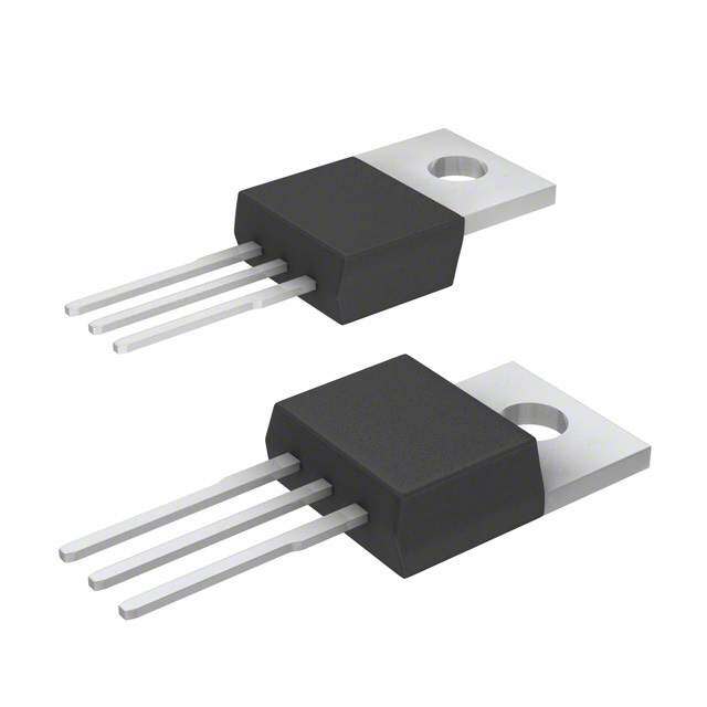
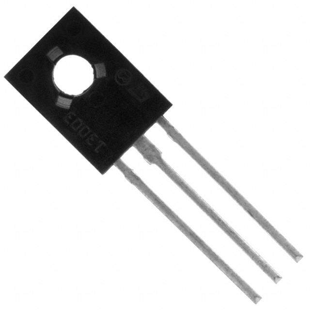
ICGOO电子元器件商城为您提供D44H11G由ON Semiconductor设计生产,在icgoo商城现货销售,并且可以通过原厂、代理商等渠道进行代购。 D44H11G价格参考。ON SemiconductorD44H11G封装/规格:晶体管 - 双极 (BJT) - 单, 双极 (BJT) 晶体管 NPN 80V 10A 50MHz 2W 通孔 TO-220AB。您可以下载D44H11G参考资料、Datasheet数据手册功能说明书,资料中有D44H11G 详细功能的应用电路图电压和使用方法及教程。
ON Semiconductor的D44H11G是一款NPN型双极晶体管(BJT),广泛应用于各种电子电路中,尤其适用于功率放大和开关应用。以下是其主要应用场景:

 1. 音频放大器
D44H11G常用于音频放大器中的功率输出级。它能够处理较大的电流和电压,适合驱动扬声器等负载。其低饱和电压和高增益特性使其在音频放大电路中表现出色,能够提供清晰、稳定的音频输出。

 2. 电源管理
在电源管理系统中,D44H11G可以用作开关元件或线性稳压器的一部分。它能够承受较高的电流和电压波动,确保电源系统的稳定性和可靠性。例如,在直流-直流转换器中,它可以作为开关管来控制电流的通断,从而实现高效的电源转换。

 3. 电机驱动
D44H11G可以用于驱动小型直流电机或步进电机。通过控制基极电流,晶体管可以在饱和区和截止区之间切换,从而实现对电机转速和方向的精确控制。它的大电流承载能力使其能够应对电机启动时的瞬态电流冲击。

 4. 继电器驱动
在需要驱动电磁继电器的应用中,D44H11G可以用作驱动晶体管。它能够提供足够的电流来激活继电器线圈,并且可以通过外部电阻来调节基极电流,确保继电器的可靠工作。此外,它还可以与光耦合器配合使用,实现电气隔离。

 5. LED驱动
对于大功率LED照明系统,D44H11G可以用作电流控制元件。通过调整基极电流,可以精确控制LED的亮度。它能够承受较大的电流,确保LED在不同工作条件下都能稳定发光。

 6. 工业自动化
在工业控制系统中,D44H11G可用于信号放大和逻辑电平转换。它可以将微弱的输入信号放大到足以驱动执行器或其他外设的水平,同时保持较低的噪声和失真。

总之,D44H11G凭借其出色的性能和可靠性,成为许多电力电子设备和控制系统中的关键元件,适用于多种功率放大和开关应用。
| 参数 | 数值 |
| 产品目录 | |
| 描述 | TRANS NPN 10A 80V TO220AB两极晶体管 - BJT 10A 80V 50W NPN |
| 产品分类 | 晶体管(BJT) - 单路分离式半导体 |
| 品牌 | ON Semiconductor |
| 产品手册 | |
| 产品图片 |
|
| rohs | 符合RoHS无铅 / 符合限制有害物质指令(RoHS)规范要求 |
| 产品系列 | 晶体管,两极晶体管 - BJT,ON Semiconductor D44H11G- |
| 数据手册 | |
| 产品型号 | D44H11G |
| PCN组件/产地 | |
| 不同 Ib、Ic时的 Vce饱和值(最大值) | 1V @ 400mA,8A |
| 不同 Ic、Vce 时的DC电流增益(hFE)(最小值) | 40 @ 4A,1V |
| 产品目录页面 | |
| 产品种类 | 两极晶体管 - BJT |
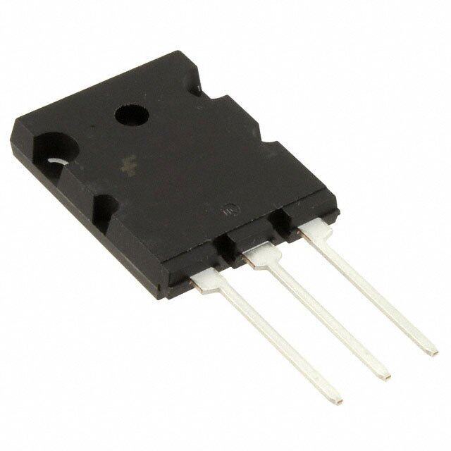
| 供应商器件封装 | TO-220AB |
| 其它名称 | D44H11GOS |
| 功率-最大值 | 2W |
| 包装 | 管件 |
| 发射极-基极电压VEBO | 5 V |
| 商标 | ON Semiconductor |
| 增益带宽产品fT | 50 MHz |
| 安装类型 | 通孔 |
| 安装风格 | Through Hole |
| 封装 | Tube |
| 封装/外壳 | TO-220-3 |
| 封装/箱体 | TO-220-3 |
| 工厂包装数量 | 50 |
| 晶体管极性 | NPN |
| 晶体管类型 | NPN |
| 最大功率耗散 | 70 W |
| 最大工作温度 | + 150 C |
| 最大直流电集电极电流 | 10 A |
| 最小工作温度 | - 55 C |
| 标准包装 | 50 |
| 电压-集射极击穿(最大值) | 80V |
| 电流-集电极(Ic)(最大值) | 10A |
| 电流-集电极截止(最大值) | 10µA |
| 直流集电极/BaseGainhfeMin | 60 |
| 系列 | D44H11 |
| 配置 | Single |
| 集电极—发射极最大电压VCEO | 80 V |
| 集电极—基极电压VCBO | 80 V |
| 集电极—射极饱和电压 | 1 V |
| 集电极连续电流 | 10 A |
| 频率-跃迁 | 50MHz |


- 商务部:美国ITC正式对集成电路等产品启动337调查
- 曝三星4nm工艺存在良率问题 高通将骁龙8 Gen1或转产台积电
- 太阳诱电将投资9.5亿元在常州建新厂生产MLCC 预计2023年完工
- 英特尔发布欧洲新工厂建设计划 深化IDM 2.0 战略
- 台积电先进制程称霸业界 有大客户加持明年业绩稳了
- 达到5530亿美元!SIA预计今年全球半导体销售额将创下新高
- 英特尔拟将自动驾驶子公司Mobileye上市 估值或超500亿美元
- 三星加码芯片和SET,合并消费电子和移动部门,撤换高东真等 CEO
- 三星电子宣布重大人事变动 还合并消费电子和移动部门
- 海关总署:前11个月进口集成电路产品价值2.52万亿元 增长14.8%


PDF Datasheet 数据手册内容提取
D44H Series (NPN), D45H(cid:2)Series (PNP) Complementary Silicon Power Transistors These series of plastic, silicon NPN and PNP power transistors can be used as general purpose power amplification and switching such as www.onsemi.com output or driver stages in applications such as switching regulators, converters and power amplifiers. 10 AMP COMPLEMENTARY SILICON POWER Features • Low Collector−Emitter Saturation Voltage TRANSISTORS 60, 80 VOLTS • Fast Switching Speeds • Complementary Pairs Simplifies Designs PNP NPN • These Devices are Pb−Free and are RoHS Compliant* COLLECTOR 2, 4 COLLECTOR 2, 4 MAXIMUM RATINGS 1 1 Rating Symbol Value Unit BASE BASE Collector−Emitter Voltage VCEO Vdc D44H8, D45H8 60 EMITTER 3 EMITTER 3 D44H11, D45H11 80 MARKING Emitter Base Voltage VEB 5.0 Vdc 4 DIAGRAM Collector Current − Continuous IC 10 Adc Collector Current − Peak (Note 1) ICM 20 Adc Total Power Dissipation PD W @ TC = 25°C 70 @ TA = 25°C 2.0 TO−220 D4xHyyG CASE 221A AYWW Operating and Storage Junction TJ, Tstg −55 to +150 °C STYLE 1 Temperature Range 1 2 3 Stresses exceeding those listed in the Maximum Ratings table may damage the device. If any of these limits are exceeded, device functionality should not be assumed, damage may occur and reliability may be affected. 1. Pulse Width ≤ 6.0 ms, Duty Cycle ≤ 50%. D4xHyy =Device Code x = 4 or 5 THERMAL CHARACTERISTICS yy = 8 or 11 A =Assembly Location Characteristic Symbol Max Unit Y =Year Thermal Resistance, Junction−to−Case R(cid:2)JC 1.8 °C/W WW =Work Week G =Pb−Free Package Thermal Resistance, Junction−to−Ambient R(cid:2)JA 62.5 °C/W MPuarxpimosuems: L1e/8a″d fTroemm pCearsaetu froer f5o rS Seoclodnedrisng TL 275 °C ORDERING INFORMATION Device Package Shipping D44H8G TO−220 50 Units/Rail (Pb−Free) D44H11G TO−220 50 Units/Rail (Pb−Free) D45H8G TO−220 50 Units/Rail (Pb−Free) *For additional information on our Pb−Free strategy and soldering details, please D45H11G TO−220 50 Units/Rail download the ON Semiconductor Soldering and Mounting Techniques (Pb−Free) Reference Manual, SOLDERRM/D. © Semiconductor Components Industries, LLC, 2014 1 Publication Order Number: November, 2014 − Rev. 13 D44H/D
D44H Series (NPN), D45H Series (PNP) ELECTRICAL CHARACTERISTICS (TC = 25°C unless otherwise noted) Characteristic Symbol Min Typ Max Unit OFF CHARACTERISTICS Collector−Emitter Sustaining Voltage D44H8, D45H8 VCEO(sus) 60 − − Vdc (IC = 30 mAdc, IB = 0 Adc) D44H11, D45H11 80 − − Collector Cutoff Current (VCE = Rated VCEO, VBE = 0) ICES − − 10 (cid:3)A Emitter Cutoff Current (VEB = 5.0 Vdc) IEBO − − 10 (cid:3)A ON CHARACTERISTICS DC Current Gain hFE − (VCE = 1.0 Vdc, IC = 2.0 Adc) 60 − − (VCE = 1.0 Vdc, IC = 4.0 Adc) 40 − − Collector−Emitter Saturation Voltage VCE(sat) Vdc (IC = 8.0 Adc, IB = 0.4 Adc) − − 1.0 Base−Emitter Saturation Voltage VBE(sat) − − 1.5 Vdc (IC = 8.0 Adc, IB = 0.8 Adc) DYNAMIC CHARACTERISTICS Collector Capacitance Ccb pF (VCB = 10 Vdc, ftest = 1.0 MHz) D44H Series − 90 − D45H Series − 160 − Gain Bandwidth Product fT MHz (IC = 0.5 Adc, VCE = 10 Vdc, f = 20 MHz) D44H Series − 50 − D45H Series − 40 − SWITCHING TIMES Delay and Rise Times td + tr ns (IC = 5.0 Adc, IB1 = 0.5 Adc) D44H Series − 300 − D45H Series − 135 − Storage Time ts ns (IC = 5.0 Adc, IB1 = IB2 = 0.5 Adc) D44H Series − 500 − D45H Series − 500 − Fall Time tf ns (IC = 5.0 Adc, IB1 = 102 = 0.5 Adc) D44H Series − 140 − D45H Series − 100 − Product parametric performance is indicated in the Electrical Characteristics for the listed test conditions, unless otherwise noted. Product performance may not be indicated by the Electrical Characteristics if operated under different conditions. www.onsemi.com 2
D44H Series (NPN), D45H Series (PNP) 1000 1000 VCE = 1 V VCE = 1 V 25°C N N AI 125°C AI G G 125°C T T EN −40°C EN 25°C R R R 100 R100 −40°C U U C C C C D D , E , E F F h h 10 10 0.01 0.1 1 10 0.01 0.1 1 10 IC, COLLECTOR CURRENT (AMPS) IC, COLLECTOR CURRENT (AMPS) Figure 1. D44H11 DC Current Gain Figure 2. D45H11 DC Current Gain 1000 1000 VCE = 5 V VCE = 5 V N 25°C N AI 125°C AI G G 125°C T T N N 25°C E E RR 100 −40°C RR100 −40°C U U C C C C D D , E , E F F h h 10 10 0.01 0.1 1 10 0.01 0.1 1 10 IC, COLLECTOR CURRENT (AMPS) IC, COLLECTOR CURRENT (AMPS) Figure 3. D44H11 DC Current Gain Figure 4. D45H11 DC Current Gain 0.40 0.6 S) 0.35 VCE(sat) @ IC/IB = 10 S) VCE(sat) @ IC/IB = 10 LT LT 0.5 O O V 0.30 V AGE ( 0.25 −40°C AGE ( 0.4 −40°C T T L L O 0.20 O 0.3 V V 25°C ON 0.15 25°C ON 125°C TI TI 0.2 RA 0.10 125°C RA U U T T 0.1 A 0.05 A S S 0 0 0.1 1 10 0.1 1 10 IC, COLLECTOR CURRENT (AMPS) IC, COLLECTOR CURRENT (AMPS) Figure 5. D44H11 ON−Voltage Figure 6. D45H11 ON−Voltage www.onsemi.com 3
D44H Series (NPN), D45H Series (PNP) 1.2 1.4 OLTS) 1.0 VBE(sat) @ IC/IB = 10 −40°C OLTS) 1.2 VBE(sat) @ IC/IB = 10 −40°C V V GE ( 0.8 125°C GE ( 1.0 TA TA 0.8 L L 125°C O 0.6 O N V 25°C N V 0.6 O O 25°C ATI 0.4 ATI 0.4 R R U U AT 0.2 AT 0.2 S S 0 0 0.1 1 10 0.1 1 10 IC, COLLECTOR CURRENT (AMPS) IC, COLLECTOR CURRENT (AMPS) Figure 7. D44H11 ON−Voltage Figure 8. D45H11 ON−Voltage 100 TA TC PS) 50 TS) M 30 T ENT (A 1200 1.0 ms 100 1(cid:3)0s (cid:3)s ON (WA 3.0 60 CTOR CURR 1235....0000 TDCU T≤ Y7 0C°Y CCLE ≤ 50% dc 1.0 (cid:3)s R DISSIPATI 2.0 40 TC E E LL 0.5 W 1.0 20 TA O O C 0.3 D44H/45H8 P , C 0.2 D44H/45H10,11 , D I P 0.1 0 0 1.0 2.0 3.0 5.0 7.0 10 20 30 50 70 100 0 20 40 60 80 100 120 140 160 VCE, COLLECTOR−EMITTER VOLTAGE (VOLTS) T, TEMPERATURE (°C) Figure 9. Maximum Rated Forward Bias Figure 10. Power Derating Safe Operating Area 1.0 0.7 D) D = 0.5 RMALALIZE 00..53 EM 0.2 THR 0.2 NT NO 0.1 ANSIEANCE (00.0.17 0.05 ZR(cid:2)(cid:2)JJCC( t=) =1 .r5(t6) °RC(cid:2)/WJC MAX P(pk) RT0.05 D CURVES APPLY FOR POWER TS 0.02 r(t), RESI0.03 PRUELASDE T TIMREA IANT S t1HOWN t1 t2 0.02 0.01 SINGLE PULSE TJ(pk) - TC = P(pk) Z(cid:2)JC(t) DUTY CYCLE, D = t1/t2 0.01 0.01 0.02 0.05 0.1 0.2 0.5 1.0 2.0 5.0 10 20 50 100 200 500 1.0 k t, TIME (ms) Figure 11. Thermal Response www.onsemi.com 4
D44H Series (NPN), D45H Series (PNP) PACKAGE DIMENSIONS TO−220 CASE 221A−09 ISSUE AH NOTES: 1. DIMENSIONING AND TOLERANCING PER ANSI Y14.5M, 1982. −T− SPELAATNIENG 2. CONTROLLING DIMENSION: INCH. 3. DIMENSION Z DEFINES A ZONE WHERE ALL B F C BODY AND LEAD IRREGULARITIES ARE T S ALLOWED. INCHES MILLIMETERS 4 DIM MIN MAX MIN MAX A 0.570 0.620 14.48 15.75 Q A B 0.380 0.415 9.66 10.53 C 0.160 0.190 4.07 4.83 1 2 3 U D 0.025 0.038 0.64 0.96 F 0.142 0.161 3.61 4.09 H G 0.095 0.105 2.42 2.66 H 0.110 0.161 2.80 4.10 K J 0.014 0.024 0.36 0.61 Z K 0.500 0.562 12.70 14.27 L 0.045 0.060 1.15 1.52 N 0.190 0.210 4.83 5.33 L R Q 0.100 0.120 2.54 3.04 R 0.080 0.110 2.04 2.79 V J S 0.045 0.055 1.15 1.39 T 0.235 0.255 5.97 6.47 G U 0.000 0.050 0.00 1.27 D V 0.045 --- 1.15 --- Z --- 0.080 --- 2.04 N STYLE 1: PIN 1. BASE 2. COLLECTOR 3. EMITTER 4. COLLECTOR ON Semiconductor and the are registered trademarks of Semiconductor Components Industries, LLC (SCILLC) or its subsidiaries in the United States and/or other countries. SCILLC owns the rights to a number of patents, trademarks, copyrights, trade secrets, and other intellectual property. A listing of SCILLC’s product/patent coverage may be accessed at www.onsemi.com/site/pdf/Patent−Marking.pdf. SCILLC reserves the right to make changes without further notice to any products herein. SCILLC makes no warranty, representation or guarantee regarding the suitability of its products for any particular purpose, nor does SCILLC assume any liability arising out of the application or use of any product or circuit, and specifically disclaims any and all liability, including without limitation special, consequential or incidental damages. “Typical” parameters which may be provided in SCILLC data sheets and/or specifications can and do vary in different applications and actual performance may vary over time. All operating parameters, including “Typicals” must be validated for each customer application by customer’s technical experts. SCILLC does not convey any license under its patent rights nor the rights of others. SCILLC products are not designed, intended, or authorized for use as components in systems intended for surgical implant into the body, or other applications intended to support or sustain life, or for any other application in which the failure of the SCILLC product could create a situation where personal injury or death may occur. Should Buyer purchase or use SCILLC products for any such unintended or unauthorized application, Buyer shall indemnify and hold SCILLC and its officers, employees, subsidiaries, affiliates, and distributors harmless against all claims, costs, damages, and expenses, and reasonable attorney fees arising out of, directly or indirectly, any claim of personal injury or death associated with such unintended or unauthorized use, even if such claim alleges that SCILLC was negligent regarding the design or manufacture of the part. SCILLC is an Equal Opportunity/Affirmative Action Employer. This literature is subject to all applicable copyright laws and is not for resale in any manner. PUBLICATION ORDERING INFORMATION LITERATURE FULFILLMENT: N. American Technical Support: 800−282−9855 Toll Free ON Semiconductor Website: www.onsemi.com Literature Distribution Center for ON Semiconductor USA/Canada P.O. Box 5163, Denver, Colorado 80217 USA Europe, Middle East and Africa Technical Support: Order Literature: http://www.onsemi.com/orderlit Phone: 303−675−2175 or 800−344−3860 Toll Free USA/Canada Phone: 421 33 790 2910 Fax: 303−675−2176 or 800−344−3867 Toll Free USA/Canada Japan Customer Focus Center For additional information, please contact your local Email: orderlit@onsemi.com Phone: 81−3−5817−1050 Sales Representative www.onsemi.com D44H/D 5
Mouser Electronics Authorized Distributor Click to View Pricing, Inventory, Delivery & Lifecycle Information: O N Semiconductor: D44H11G D44H8G D45H11G D45H8G