ICGOO在线商城 > 集成电路(IC) > 嵌入式 - 微控制器 - 应用特定 > CY8C20237-24SXI
 Datasheet下载
- 型号: CY8C20237-24SXI
- 制造商: Cypress Semiconductor
- 库位|库存: xxxx|xxxx
- 要求:
| 数量阶梯 | 香港交货 | 国内含税 |
| +xxxx | $xxxx | ¥xxxx |
查看当月历史价格
查看今年历史价格
CY8C20237-24SXI产品简介:
ICGOO电子元器件商城为您提供CY8C20237-24SXI由Cypress Semiconductor设计生产,在icgoo商城现货销售,并且可以通过原厂、代理商等渠道进行代购。 CY8C20237-24SXI价格参考。Cypress SemiconductorCY8C20237-24SXI封装/规格:嵌入式 - 微控制器 - 应用特定, 。您可以下载CY8C20237-24SXI参考资料、Datasheet数据手册功能说明书,资料中有CY8C20237-24SXI 详细功能的应用电路图电压和使用方法及教程。
型号为CY8C20237-24SXI的芯片,属于Cypress Semiconductor Corp(赛普拉斯半导体公司)旗下的PSoC(可编程系统级芯片)系列,是一款集成了微控制器和可配置模拟/数字外设的嵌入式控制器。该芯片主要面向特定应用场景,具备高集成度和灵活性,适用于多种嵌入式控制系统。

应用场景主要包括:

1. 消费类电子产品:如智能家电、智能水杯、电动牙刷等,用于实现触控感应、LED控制、电机驱动等功能。

2. 工业控制:用于传感器控制、小型电机控制、工业自动化设备中的用户界面管理。

3. 汽车电子:应用于车载控制面板、车内照明控制、车门模块等,支持汽车环境中对可靠性和稳定性的要求。

4. 物联网(IoT)设备:作为主控芯片用于低功耗传感器节点、无线通信模块的控制核心,支持连接和数据处理功能。

5. 便携式设备:如智能手环、健康监测设备等,因其低功耗特性,适合电池供电系统。

该芯片内置M8C处理器,支持CapSense电容式触摸感应技术,适合用于需要人机交互界面的设计。其高集成度减少了外围元件需求,有助于降低系统成本和设计复杂度。
| 参数 | 数值 |
| 产品目录 | 集成电路 (IC)半导体 |
| 描述 | IC CAPSENCE 8K FLASH 16SOIC8位微控制器 -MCU 1.8V CapSense Ctrl W/SmartSense |
| 产品分类 | |
| I/O数 | 14 |
| 品牌 | Cypress Semiconductor |
| 产品手册 | http://www.cypress.com/?docID=49787 |
| 产品图片 |
|
| rohs | 符合RoHS无铅 / 符合限制有害物质指令(RoHS)规范要求 |
| 产品系列 | 微控制器 - MCU,8位微控制器 -MCU,Cypress Semiconductor CY8C20237-24SXICapSense® 控制器 |
| 数据手册 | |
| 产品型号 | CY8C20237-24SXI |
| PCN其它 | http://www.cypress.com/?docID=45911 |
| PCN组件/产地 | http://www.cypress.com/?docID=44762http://www.cypress.com/?docID=48110http://www.cypress.com/?docID=49128 |
| RAM容量 | 1K x 8 |
| 产品种类 | 8位微控制器 -MCU |
| 供应商器件封装 | 16-SOIC |
| 包装 | 管件 |
| 商标 | Cypress Semiconductor |
| 商标名 | CapSense |
| 处理器系列 | CY8C20x37 |
| 安装类型 | 表面贴装 |
| 安装风格 | SMD/SMT |
| 封装 | Tube |
| 封装/外壳 | 16-SOIC(0.154",3.90mm 宽) |
| 封装/箱体 | SOIC-16 |
| 工作温度 | -40°C ~ 85°C |
| 工作温度范围 | 0 C to + 70 C |
| 工作电源电压 | 1.71 V to 5.5 V |
| 工厂包装数量 | 48 |
| 应用 | 电容式传感 |
| 接口 | I²C, SPI |
| 接口类型 | I2C, SPI |
| 控制器系列 | CY8C20xx7/S |
| 数据RAM大小 | 1 kB |
| 数据总线宽度 | 8 bit |
| 最大时钟频率 | 24 MHz |
| 标准包装 | 48 |
| 核心 | M8C |
| 核心处理器 | M8C |
| 片上ADC | Yes |
| 电压-电源 | 1.71 V ~ 5.5 V |
| 程序存储器大小 | 8 kB |
| 程序存储器类型 | 闪存(8 kB) |
| 系列 | CY8C20237 |


- 商务部:美国ITC正式对集成电路等产品启动337调查
- 曝三星4nm工艺存在良率问题 高通将骁龙8 Gen1或转产台积电
- 太阳诱电将投资9.5亿元在常州建新厂生产MLCC 预计2023年完工
- 英特尔发布欧洲新工厂建设计划 深化IDM 2.0 战略
- 台积电先进制程称霸业界 有大客户加持明年业绩稳了
- 达到5530亿美元!SIA预计今年全球半导体销售额将创下新高
- 英特尔拟将自动驾驶子公司Mobileye上市 估值或超500亿美元
- 三星加码芯片和SET,合并消费电子和移动部门,撤换高东真等 CEO
- 三星电子宣布重大人事变动 还合并消费电子和移动部门
- 海关总署:前11个月进口集成电路产品价值2.52万亿元 增长14.8%

PDF Datasheet 数据手册内容提取
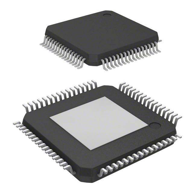
CY8C20xx7/S ® 1.8 V CapSense Controller with SmartSense™ Auto-tuning 31 Buttons, 6 Sliders, Proximity Sensors 1.8 V CapSense® Controller with SmartSense™ Auto-tuning 31 Buttons, 6 Sliders, Proximity Sensors Features ■4 Clock Sources ❐Internal main oscillator (IMO): 6/12/24 MHz ■QuietZone™ Controller ❐Internal low-speed oscillator (ILO) at 32 kHz for watchdog ❐Patented Capacitive Sigma Delta PLUS (CSD PLUS™) and sleep timers sensing algorithm for robust performance ❐External 32 KHz Crystal Oscillator ❐High Sensitivity (0.1 pF) and best-in-class SNR performance ❐External Clock Input to support: ■Programmable pin configurations • Overlay thickness of 15 mm for glass and 5 mm plastic ❐Up to 34 general-purpose I/Os (GPIOs) • Proximity Solutions ❐Dual mode GPIO (Analog and Digital) ❐Superior noise immunity performance against conducted and radiated noise and ultra low radiated emissions ❐High sink current of 25 mA per GPIO • Standardized user modules for overcoming noise • Max sink current 120 mA for all I/Os combined ❐Source Current ■Low power CapSense® block with SmartSense Auto-tuning • 5 mA on ports 0 and 1 ❐Low average power consumption – • 1 mA on ports 2, 3 and 4 • 28 µA/sensor in run time (wake-up and scan once every ❐Configurable internal pull-up, high-Z and open drain modes 125 ms) ❐Selectable, regulated digital I/O on port 1 ❐SmartSense_EMC_PLUS Auto-Tuning ❐Configurable input threshold on port 1 • Sets and maintains optimal sensor performance during run time ■Versatile Analog functions • Eliminates system tuning during development and ❐Internal analog bus supports connection of multiple sensors production to form ganged proximity sensor • Compensates for variations in manufacturing process ❐Internal Low-Dropout voltage regulator for high power supply rejection ratio (PSRR) ■Driven shield available on five GPIO pins ■Additional system resources ❐Delivers best-in class water tolerant designs ❐I2C Slave: ❐Robust proximity sensing in the presence of metal objects • Selectable to 50 kHz, 100 kHz, or 400 kHz ❐Supports longer trace lengths • Selectable Clock stretch or Forced Nack Mode ❐Max load of 100 pF (3 MHz) • I2C wake from sleep with Hardware address match ■Powerful Harvard-architecture processor ❐12 MHz (Configurable) SPI master and slave ❐M8C CPU with a max speed of 24 MHz ❐Three 16-bit timers ■Operating Range: 1.71 V to 5.5 V ❐Watchdog and sleep timers ❐Standby Mode 1.1 μA (Typ) ❐Integrated supervisory circuit ❐Deep Sleep 0.1 μA (Typ) ❐10-bit incremental analog-to-digital converter (ADC) with internal voltage reference ■Operating Temperature range: –40oC to +85oC ❐Two general-purpose high speed, low power analog comparators ■Flexible on-chip memory ❐8 KB flash, 1 KB SRAM ■Complete development tools ❐16 KB flash, 2 KB SRAM ❐Free development tool (PSoC Designer™) ❐32 KB flash, 2 KB SRAM ■Sensor and Package options ❐50,000 flash erase/write cycles ❐10 Sensing Inputs – 16-pin QFN, 16-pin SOIC ❐Read while Write with EEPROM emulation ❐16 Sensing Inputs – 24-pin QFN ❐In-system programming simplifies manufacturing process ❐24 Sensing Inputs – 30-pin WLCSP ❐25 Sensing Inputs – 32-pin QFN ❐31 Sensing Inputs – 48-pin QFN Errata: For information on silicon errata, see “Errata” on page38. Details include trigger conditions, devices affected, and proposed workaround. CypressSemiconductorCorporation • 198 Champion Court • SanJose, CA 95134-1709 • 408-943-2600 Document Number: 001-69257 Rev. *Q Revised May 11, 2018
CY8C20xx7/S Logic Block Diagram Port 4 Port 3 Port 2 Port 1 Port 0 1.8/2.5/3V PWRSYS[1] LDO (Regulator) PSoC CORE SYSTEM BUS Global Analog Interconnect 1K/2K 8K/16K/32KFlash SRAM Supervisory ROM ( SROM) Nonvolatile Memory Interrupt Sleep and Controller CPU Core (M8C) Watchdog 6/12/24 M Hz Internal Main Oscillator (IMO) Internal Low Speed Oscillator (ILO) Multiple Clock Sources CAPSENSE Analog SYSTEM Reference CapSense Comparator #1 Module Analog Comparator #2 Mux SYSTEM BUS I2C Internal System POR SPI Three 16-Bit Digital Slave Voltage Resets and Master/ Programmable Clocks References LVD Slave Timers SYSTEM RESOURCES Note 1. Internal voltage regulator for internal circuitry Document Number: 001-69257 Rev. *Q Page 2 of 46
CY8C20xx7/S Contents PSoC® Functional Overview ............................................4 Shield Driver DC Specifications ................................20 PSoC Core ..................................................................4 DC IDAC Specifications ............................................20 CapSense System .......................................................4 AC Chip-Level Specifications ....................................21 Additional System Resources .....................................5 AC General Purpose I/O Specifications ....................22 Getting Started ..................................................................5 AC Comparator Specifications ..................................22 Application Notes/Design Guides ................................5 AC External Clock Specifications ..............................22 Development Kits ........................................................5 AC Programming Specifications ................................23 Training .......................................................................5 AC I2C Specifications ................................................24 CYPros Consultants ....................................................5 Packaging Information ...................................................27 Solutions Library ..........................................................5 Thermal Impedances .................................................30 Technical Support .......................................................5 Capacitance on Crystal Pins .....................................30 Designing with PSoC Designer .......................................6 Solder Reflow Peak Temperature .............................30 Select Components .....................................................6 Development Tool Selection .........................................31 Configure Components ...............................................6 Software ....................................................................31 Organize and Connect ................................................6 Development Kits ......................................................31 Generate, Verify, and Debug .......................................6 Evaluation Tools ........................................................31 Pinouts ..............................................................................7 Device Programmers .................................................32 16-pin SOIC (10 Sensing Inputs) ................................7 Third Party Tools .......................................................32 16-pin QFN (10 Sensing Inputs)[9] ..............................8 Ordering Information ......................................................33 24-pin QFN (16 Sensing Inputs)[15] ............................9 Ordering Code Definitions .........................................34 30-ball WLCSP (24 Sensing Inputs) ..........................10 Acronyms ........................................................................35 32-pin QFN (25 Sensing Inputs)[26] ..........................11 Reference Documents ....................................................35 48-pin QFN (31 Sensing Inputs)[32] ..........................12 Document Conventions .............................................35 Electrical Specifications ................................................13 Units of Measure .......................................................35 Absolute Maximum Ratings .......................................13 Numeric Naming ........................................................36 Operating Temperature .............................................13 Glossary ..........................................................................36 DC Chip-Level Specifications ....................................14 Errata ...............................................................................37 DC GPIO Specifications ............................................15 CY8C20xx7/S Qualification Status ............................37 DC Analog Mux Bus Specifications ...........................17 CY8C20xx7/S Errata Summary .................................37 DC Low Power Comparator Specifications ...............17 Document History Page .................................................41 Comparator User Module Electrical Specifications ...18 Sales, Solutions, and Legal Information ......................45 ADC Electrical Specifications ....................................18 Worldwide Sales and Design Support .......................45 DC POR and LVD Specifications ..............................19 DC Programming Specifications ...............................19 DC I2C Specifications ...............................................20 Document Number: 001-69257 Rev. *Q Page 3 of 46
CY8C20xx7/S PSoC® Functional Overview Figure 1. CapSense System Block Diagram The PSoC family consists of many devices with on-chip CS1 controllers. These devices are designed to replace multiple traditional MCU-based system components with one low-cost IDAC single-chip programmable component. A PSoC device includes s CS2 configurable blocks of analog and digital logic, and Bu programmable interconnect. This architecture makes it possible bal o for you to create customized peripheral configurations, to match Gl the requirements of each individual application. Additionally, a og fast central processing unit (CPU), flash program memory, nal CSN A SRAM data memory, and configurable I/O are included in a Vr range of convenient pinouts. The architecture for this device family, as shown in the “Logic Reference Block Diagram” on page2, consists of three main areas: Buffer ■The core ■CapSense analog system Comparator Cexternal (P0[1] Mux or P0[3]) ■System resources Mux Refs A common, versatile bus allows connection between I/O and the analog system. Each CY8C20x37/47/67/S PSoC device includes a dedicated CapSense block that provides sensing and scanning control Cap Sense Counters circuitry for capacitive sensing applications. Depending on the PSoC package, up to 34 GPIOs are also included. The GPIOs provide access to the MCU and analog mux. CSCLK PSoC Core IMO CapSense Oscillator Clock Select The PSoC core is a powerful engine that supports a rich instruction set. It encompasses SRAM for data storage, an interrupt controller, sleep and watchdog timers, and IMO and ILO. The CPU core, called the M8C, is a powerful processor with Analog Multiplexer System speeds up to 24 MHz. The M8C is a 4-million instructions per second (MIPS), 8-bit Harvard-architecture microprocessor. The analog mux bus can connect to every GPIO pin. Pins are connected to the bus individually or in any combination. The bus CapSense System also connects to the analog system for analysis with the The analog system contains the capacitive sensing hardware. CapSense block comparator. Several hardware algorithms are supported. This hardware Switch-control logic enables selected pins to precharge performs capacitive sensing and scanning without requiring continuously under hardware control. This enables capacitive external components. The analog system is composed of the measurement for applications such as touch sensing. Other CapSense PSoC block and an internal 1 V or 1.2 V analog multiplexer applications include: reference, which together support capacitive sensing of up to 31 inputs[2]. Capacitive sensing is configurable on each GPIO pin. ■Complex capacitive sensing interfaces, such as sliders and Scanning of enabled CapSense pins is completed quickly and touchpads. easily across multiple ports. ■Chip-wide mux that allows analog input from any I/O pin. SmartSense™ Auto-tuning ■Crosspoint connection between any I/O pin combinations. SmartSense auto-tuning is an innovative solution from Cypress that removes manual tuning of CapSense applications. This solution is easy to use and provides robust noise immunity. It is the only auto-tuning solution that establishes, monitors, and maintains all required tuning parameters of each sensor during run time. SmartSense auto-tuning allows engineers to go from prototyping to mass production without retuning for manufacturing variations in PCB and/or overlay material properties. Note 2. 34 GPIOs = 31 pins for capacitive sensing+2 pins for I2C + 1 pin for modulator capacitor. Document Number: 001-69257 Rev. *Q Page 4 of 46
CY8C20xx7/S Additional System Resources Getting Started System resources provide additional capability, such as configurable I2C slave, SPI master/slave communication The quickest way to understand PSoC silicon is to read this datasheet and then use the PSoC Designer Integrated interface, three 16-bit programmable timers, various system Development Environment (IDE). This datasheet is an overview resets supported by the M8C low voltage detection and power- of the PSoC integrated circuit and presents specific pin, register, on reset. The merits of each system resource are listed here: and electrical specifications. ■The I2C slave/SPI master-slave module provides 50/100/ For in depth information, along with detailed programming 400kHz communication over two wires. SPI communication details, see the Technical Reference Manual for the CY8C20x37/ over three or four wires runs at speeds of 46.9 kHz to 3MHz 47/67/S PSoC devices. (lower for a slower system clock). For up-to-date ordering, packaging, and electrical specification ■The I2C hardware address recognition feature reduces the information, see the latest PSoC device datasheets on the web already low power consumption by eliminating the need for at www.cypress.com/psoc. CPU intervention until a packet addressed to the target device is received. Application Notes/Design Guides ■The I2C enhanced slave interface appears as a 32-byte RAM Application notes and design guides are an excellent buffer to the external I2C master. Using a simple predefined introduction to the wide variety of possible PSoC designs. They protocol, the master controls the read and write pointers into are located at www.cypress.com/gocapsense. Select the RAM. When this method is enabled, the slave does not stall Application Notes under the Related Documentation tab. the bus when receiving data bytes in active mode. For more Development Kits details, refer to the I2CSBUF User Module datasheet. PSoC Development Kits are available online from Cypress at ■Low-voltage detection (LVD) interrupts can signal the www.cypress.com/shop and through a growing number of application of falling voltage levels, while the advanced power- regional and global distributors, which include Arrow, Avnet, Digi- on reset (POR) circuit eliminates the need for a system Key, Farnell, Future Electronics, and Newark. See “Development supervisor. Kits” on page32. ■An internal reference provides an absolute reference for capacitive sensing. Training ■A register-controlled bypass mode allows the user to disable Free PSoC and CapSense technical training (on demand, the LDO regulator. webinars, and workshops) is available online at www.cypress.com/training. The training covers a wide variety of topics and skill levels to assist you in your designs. CYPros Consultants Certified PSoC Consultants offer everything from technical assistance to completed PSoC designs. To contact or become a PSoC Consultant go to www.cypress.com/cypros. Solutions Library Visit our growing library of solution focused designs at www.cypress.com/solutions. Here you can find various application designs that include firmware and hardware design files that enable you to complete your designs quickly. Technical Support For assistance with technical issues, search KnowledgeBase articles and forums at www.cypress.com/support. If you cannot find an answer to your question, create a technical support case or call technical support at 1-800-541-4736. Document Number: 001-69257 Rev. *Q Page 5 of 46
CY8C20xx7/S Designing with PSoC Designer Organize and Connect The PSoC development process can be summarized in the You build signal chains at the chip level by interconnecting user following four steps: modules to each other and the I/O pins. You perform the selection, configuration, and routing so that you have complete 1.Select User Modules control over all on-chip resources. 2.Configure User Modules Generate, Verify, and Debug 3.Organize and Connect When you are ready to test the hardware configuration or move 4.Generate and Verify on to developing code for the project, you perform the “Generate Select Components Configuration Files” step. This causes PSoC Designer to generate source code that automatically configures the device to PSoC Designer provides a library of pre-built, pre-tested your specification and provides the software for the system. The hardware peripheral components called “user modules”. User generated code provides application programming interfaces modules make selecting and implementing peripheral devices, (APIs) with high-level functions to control and respond to both analog and digital, simple. hardware events at run time and interrupt service routines that Configure Components you can adapt as needed. Each of the User Modules you select establishes the basic A complete code development environment allows you to register settings that implement the selected function. They also develop and customize your applications in C, assembly provide parameters and properties that allow you to tailor their language, or both. precise configuration to your particular application. The user module parameters permit you to establish the pulse width and duty cycle. Configure the parameters and properties to correspond to your chosen application. Enter values directly or by selecting values from drop-down menus. All the user modules are documented in datasheets that may be viewed directly in PSoC Designer or on the Cypress website. These user module datasheets explain the internal operation of the User Module and provide performance specifications. Each datasheet describes the use of each user module parameter, and other information you may need to successfully implement your design. Document Number: 001-69257 Rev. *Q Page 6 of 46
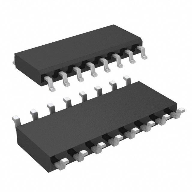
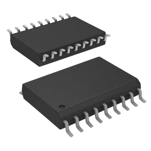
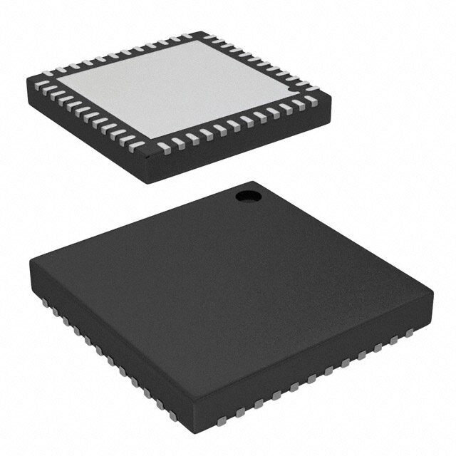
CY8C20xx7/S Pinouts The CY8C20x37/47/67/S PSoC device is available in a variety of packages, which are listed and illustrated in the following tables. Every port pin (labeled with a “P”) is capable of digital I/O and connection to the common analog bus. However, V , V , and XRES SS DD are not capable of digital I/O. 16-pin SOIC (10 Sensing Inputs) Table 1. Pin Definitions – CY8C20237-24SXI, CY8C20247/S-24SXI [3] Pin Type Figure 2. CY8C20237-24SXI, CY8C20247/S-24SXI No. Digital Analog Name Description Device 1 I/O I P0[3] Integrating Input AI, P0[3] 1 16 P0[7], AI 2 I/O I P0[1] Integrating Input AI, P0[1] 2 15 VDD AI, P2[5] 3 14 P0[4], AI 3 I/O I P2[5] Crystal output (XOut) AI, P2[3] 4 SOIC 13 XRES AI, P1[7] 5 12 P1[4], EXTCLK 4 I/O I P2[3] Crystal input (XIn) AI, P1[5] 6 11 P1[2], AI AI, P1[3] 7 10 P1[0], ISSP DATA, I2C SDA, SPI CLK, AI 5 I/O I P1[7] I2C SCL, SPI SS AI, ISSP CLK, I2C SCL, SPI MOSI, P1[1] 8 9 VSS 6 I/O I P1[5] I2C SDA, SPI MISO 7 I/O I P1[3] 8 I/O I P1[1] ISSP CLK[4], I2C SCL, SPI MOSI 9 Power V Ground connection[7] SS 10 I/O I P1[0] ISSP DATA[4], I2C SDA, SPI CLK[5] 11 I/O I P1[2] Driven Shield Output (optional) 12 I/O I P1[4] Optional external clock (EXTCLK) 13 INPUT XRES Active high external reset with internal pull-down[6] 14 I/O I P0[4] 15 Power V Supply voltage DD 16 I/O I P0[7] LEGEND A = Analog, I = Input, O = Output, OH = 5 mA High Output Drive, R = Regulated Output. Notes 3. 13 GPIOs = 10 pins for capacitive sensing+2 pins for I2C + 1 pin for modulator capacitor. 4. On Power-up, the SDA(P1[0]) drives a strong high for 256 sleep clock cycles and drives resistive low for the next 256 sleep clock cycles. The SCL(P1[1]) line drives resistive low for 512 sleep clock cycles and both the pins transition to High impedance state. On reset, after XRES de- asserts, the SDA and the SCL lines drive resistive low for 8 sleep clock cycles and transition to high impedance state. In both cases, a pull-up resistance on these lines combines with the pull-down resistance (5.6K ohm) and form a potential divider. Hence, during power-up or reset event, P1[1] and P1[0] may disturb the I2C bus. Use alternate pins if you encounter issues. 5. Alternate SPI clock. 6. The internal pull down is 5KOhm. 7. All VSS pins should be brought out to one common GND plane. Document Number: 001-69257 Rev. *Q Page 7 of 46
CY8C20xx7/S 16-pin QFN (10 Sensing Inputs)[8] Table 2. Pin Definitions – CY8C20237, CY8C20247/S [9] Pin Type Figure 3. CY8C20237, CY8C20247/S Device Name Description N1o. DiIg/Oital AnaIlog P2[5] Crystal output (XOut) P0[1], AIP0[3], AIP0[7], AIVDD 2 I/O I P2[3] Crystal input (XIn) 3 IOHR I P1[7] I2C SCL, SPI SS AI, XOut, P2[5] 11615 141312 P0[4], AI 4 IOHR I P1[5] I2C SDA, SPI MISO AI, I2C SCL, SAPII, SXSIn, ,P P12[7[3]] 23(ToQp FVNiew)1101 PX1R[E4]S, EXTCLK, AI 5 IOHR I P1[3] SPI CLK AI, I2C SDA, SPI MISO, P1[5] 4 9 P1[2], AI 56 7 8 ISSP CLK[10], I2C SCL, SPI 6789 IIIOOOHHHRRRPower III PPPV111S[[[210S]]] DMGICSrLrOSiovKPSue[1n InD1d ]SA chToiAen[ln1d0e ]Oc, tIui2otCpnu [S1t3 D(]oAp,t iSoPnaI l) KAI, SPI CL, P1[3]LK, SPI MOSI, P1[1] VSSKSDA, SPI CL, P1[0] Optional external clock P C 2C 10 IOHR I P1[4] (EXTCLK) AI,ISS ATA, I Active high external reset with D 11 Input XRES internal pull-down[12] SP S I 12 IOH I P0[4] AI, 13 Power V Supply voltage DD 14 IOH I P0[7] 15 IOH I P0[3] Integrating input 16 IOH I P0[1] Integrating input LEGEND A = Analog, I = Input, O = Output, OH = 5 mA High Output Drive, R = Regulated Output. Notes 8. No center pad. 9. 13 GPIOs = 10 pins for capacitive sensing+2 pins for I2C + 1 pin for modulator capacitor. 10.On Power-up, the SDA(P1[0]) drives a strong high for 256 sleep clock cycles and drives resistive low for the next 256 sleep clock cycles. The SCL(P1[1]) line drives resistive low for 512 sleep clock cycles and both the pins transition to High impedance state. On reset, after XRES de- asserts, the SDA and the SCL lines drive resistive low for 8 sleep clock cycles and transition to high impedance state. In both cases, a pull-up resistance on these lines combines with the pull-down resistance (5.6K ohm) and form a potential divider. Hence, during power-up or reset event, P1[1] and P1[0] may disturb the I2C bus. Use alternate pins if you encounter issues. 11.Alternate SPI clock. 12.The internal pull down is 5KOhm. 13.All VSS pins should be brought out to one common GND plane. Document Number: 001-69257 Rev. *Q Page 8 of 46
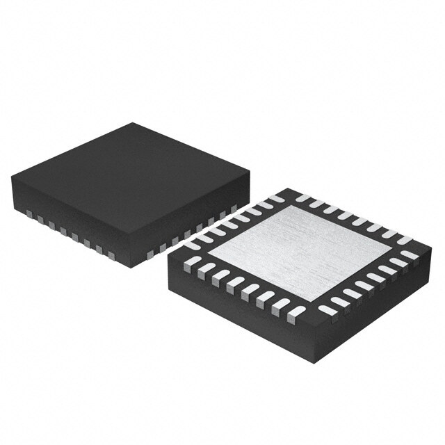
CY8C20xx7/S 24-pin QFN (16 Sensing Inputs)[14] Table 3. Pin Definitions – CY8C20337, CY8C20347/S [15] Pin Type Figure 4. CY8C20337, CY8C20347/S Device Name Description 1No. DiIg/Oital AnaIlog P2[5] Crystal output (XOut) P0[1], AI VSSP0[3], AIP0[7], AI VDDP0[4], AI 2 I/O I P2[3] Crystal input (XIn) 3 I/O I P2[1] AI, XOut, P2[5] 124 23 22 21 20 1918 P0[2], AI 4 IOHR I P1[7] I2C SCL, SPI SS AI, XIn, P2[3] 2 17 P0[0], AI AI, P2[1] 3 QFN 16 P2[4], AI 5 IOHR I P1[5] I2C SDA, SPI MISO AI, I2C SCL, SPI SS, P1[7] 4 (Top View) 15 P2[2], AI 6 IOHR I P1[3] SPI CLK AI, I2C SDA, SPI MISO, P1[5] 5 14 XRES AI, SPI CLK, P1[3] 6 13 P1[6], AI 7 IOHR I P1[1] ISSP CLK[16], I2C SCL, SPI 7 8 9 10 1112 MOSI 891110 IIOOHHRRPower II NVPP11SCS[[02]] NGC(IDSooLrrpSiov KtcPuieo[o1n nDnn7d a]ASn lceTh)oAcient[il1nod6en ]O,c It2uioCtpn Su[1tD9 ]A, SPI 2AI, ISSP CLK, I2C SCLSPI MOSI, P1[1]NCVSS2A, I2C SDA, SPI CLK, P1[0]AI, P1[2]AI, EXTCLK, P1[4] T 12 IOHR I P1[4] Optional external clock input DA (EXTCLK) SP S 13 IOHR I P1[6] AI, I 14 Input XRES Active high external reset with internal pull-down[18] 15 I/O I P2[2] Driven Shield Output (optional) 16 I/O I P2[4] Driven Shield Output (optional) 17 IOH I P0[0] Driven Shield Output (optional) 18 IOH I P0[2] Driven Shield Output (optional) 19 IOH I P0[4] 20 Power V Supply voltage DD 21 IOH I P0[7] 22 IOH I P0[3] Integrating input 23 Power V Ground connection[19] SS 24 IOH I P0[1] Integrating input CP Power V Center pad must be SS connected to ground LEGEND A = Analog, I = Input, O = Output, OH = 5 mA High Output Drive, R = Regulated Output. Notes 14.The center pad (CP) on the QFN package must be connected to ground (VSS) for best mechanical, thermal, and electrical performance. If not connected to ground, it must be electrically floated and not connected to any other signal. 15.19 GPIOs = 16 pins for capacitive sensing+2 pins for I2C + 1 pin for modulator capacitor. 16.On Power-up, the SDA(P1[0]) drives a strong high for 256 sleep clock cycles and drives resistive low for the next 256 sleep clock cycles. The SCL(P1[1]) line drives resistive low for 512 sleep clock cycles and both the pins transition to High impedance state. On reset, after XRES de- asserts, the SDA and the SCL lines drive resistive low for 8 sleep clock cycles and transition to high impedance state. In both cases, a pull-up resistance on these lines combines with the pull-down resistance (5.6K ohm) and form a potential divider. Hence, during power-up or reset event, P1[1] and P1[0] may disturb the I2C bus. Use alternate pins if you encounter issues. 17.Alternate SPI clock. 18.The internal pull down is 5KOhm. 19.All VSS pins should be brought out to one common GND plane. Document Number: 001-69257 Rev. *Q Page 9 of 46
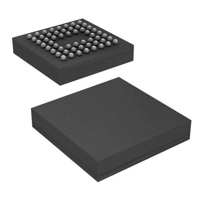
CY8C20xx7/S 30-ball WLCSP (24 Sensing Inputs) Table 4. Pin Definitions – CY8C20767, CY8C20747 30-ball Part Pinout (WLCSP) [20] Type Pin No. Name Description Figure 5. CY8C20767, CY8C20747 30-ball Digital Analog WLCSP A1 IOH I P0[2] Driven Shield Output (optional) Bottom View A2 IOH I P0[6] 5 4 3 2 1 A3 Power V Supply voltage DD A A4 IOH I P0[1] Integrating Input A5 I/O I P2[7] B B1 I/O I P4[2] B2 IOH I P0[0] Driven Shield Output (optional) C B3 IOH I P0[4] B4 IOH I P0[3] Integrating Input D B5 I/O I P2[5] Crystal Output (Xout) E C1 I/O I P2[2] Driven Shield Output (optional) C2 I/O I P2[4] Driven Shield Output (optional) F C3 I/O I P0[7] C4 IOH I P3[2] Top View C5 I/O I P2[3] Crystal Input (Xin) D1 I/O I P2[0] 1 2 3 4 5 D2 I/O I P3[0] A D3 I/O I P3[1] D4 I/O I P3[3] B D5 I/O I P2[1] Active high external reset with C E1 Input XRES internal pull-down[21] E2 IOHR I P1[6] D Optional external clock input E3 IOHR I P1[4] (EXT CLK) E E4 IOHR I P1[7] I2C SCL, SPI SS F E5 IOHR I P1[5] I2C SDA, SPI MISO F1 IOHR I P1[2] Driven Shield Output (optional) ISSP DATA[22], I2C SDA, SPI F2 IOHR I P1[0] CLK[23] F3 Power V Supply ground[24] SS ISSP CLK[22], I2C SCL, SPI F4 IOHR I P1[1] MOSI F5 IOHR I P1[3] SPI CLK LEGEND: A = Analog, I = Input, O = Output, OH = 5 mA High Output Drive, R = Regulated Output Notes 20.27 GPIOs = 24 pins for capacitive sensing+2 pins for I2C + 1 pin for modulator capacitor. 21.The internal pull down is 5KOhm. 22.On Power-up, the SDA(P1[0]) drives a strong high for 256 sleep clock cycles and drives resistive low for the next 256 sleep clock cycles. The SCL(P1[1]) line drives resistive low for 512 sleep clock cycles and both the pins transition to High impedance state. On reset, after XRES de- asserts, the SDA and the SCL lines drive resistive low for 8 sleep clock cycles and transition to high impedance state. In both cases, a pull-up resistance on these lines combines with the pull-down resistance (5.6K ohm) and form a potential divider. Hence, during power-up or reset event, P1[1] and P1[0] may disturb the I2C bus. Use alternate pins if you encounter issues. 23.Alternate SPI clock. 24.All VSS pins should be brought out to one common GND plane. Document Number: 001-69257 Rev. *Q Page 10 of 46
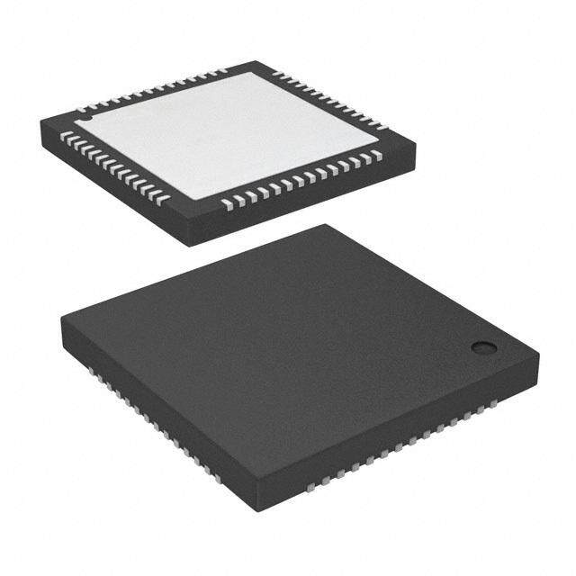
CY8C20xx7/S 32-pin QFN (25 Sensing Inputs)[25] Table 5. Pin Definitions – CY8C20437, CY8C20447/S, CY8C20467/S [26] Pin Type Figure 6. CY8C20437, CY8C20447/S, CY8C20467/S Device Name Description No. Digital Analog AIAI AI AI AIAI 12 IIO/OH II PP02[[15]] ICnrtyesgtraalt ionugt pinupt u(XtOut) VssP0[3],P0[7],VDDP0[6], P0[4], P0[2],P0[0], 3 I/O I P2[3] Crystal input (XIn) 21 09 87 65 33 32 22 22 4 I/O I P2[1] AI, P0[1] 1 24 P2[4], AI AI, XOut, P2[5] 2 23 P2[2], AI 5 I/O I P4[3] AI, XIn, P2[3] 3 22 P2[0], AI 6 I/O I P3[3] AI, P2[1] 4 QFN 21 P4[2], AI 7 I/O I P3[1] AI, P4[3] 5 (Top View) 20 P4[0], AI AI, P3[3] 6 19 P3[2], AI 8 IOHR I P1[7] I2C SCL, SPI SS AI, P3[1] 7 18 P3[0], AI 9 IOHR I P1[5] I2C SDA, SPI MISO AI, I2C SCL, SPI SS, P1[7] 8 17 XRES 9 012 34 56 111 11 11 10 IOHR I P1[3] SPI CLK. 11 IOHR I P1[1] MISOSSP IC. LK[27], I2C SCL, SPI P1[5]P1[3] P1[1] VssP1[0] P1[2] P1[4]P1[6] 1123 IOHRPower I VP1SS[0] GSISPrSoI PuCn DLdKA c[T2oA8n][n27e]c, tIi2oCn [3S0D]A, A,SPIMISO,AI,SPICLK, CL,SPIMOSI, SDA,SPICLK, AI, AI,EXTCLK,AI, 14 IOHR I P1[2] Driven Shield Output (optional) D S C S C 2 15 IOHR I P1[4] O(EpXtiToCnaLlK e)xternal clock input AI,I2C CLK,I2 ATA,ID 16 IOHR I P1[6] P P S S S S 17 Input XRES Ainctetirvnea hl ipguhl l-edxotewrnn[a29l ]reset with AII, AII, 18 I/O I P3[0] 19 I/O I P3[2] 20 I/O I P4[0] 21 I/O I P4[2] 22 I/O I P2[0] 23 I/O I P2[2] Driven Shield Output (optional) 24 I/O I P2[4] Driven Shield Output (optional) 25 IOH I P0[0] Driven Shield Output (optional) 26 IOH I P0[2] Driven Shield Output (optional) 27 IOH I P0[4] 28 IOH I P0[6] 29 Power V DD 30 IOH I P0[7] 31 IOH I P0[3] Integrating input 32 Power V Ground connection[30] SS CP Power V Center pad must be connected to SS ground LEGEND A = Analog, I = Input, O = Output, OH = 5 mA High Output Drive, R = Regulated Output. Notes 25.The center pad (CP) on the QFN package must be connected to ground (VSS) for best mechanical, thermal, and electrical performance. If not connected to ground, it must be electrically floated and not connected to any other signal. 26.28 GPIOs = 25 pins for capacitive sensing+2 pins for I2C + 1 pin for modulator capacitor. 27.On Power-up, the SDA(P1[0]) drives a strong high for 256 sleep clock cycles and drives resistive low for the next 256 sleep clock cycles. The SCL(P1[1]) line drives resistive low for 512 sleep clock cycles and both the pins transition to High impedance state. On reset, after XRES de- asserts, the SDA and the SCL lines drive resistive low for 8 sleep clock cycles and transition to high impedance state. In both cases, a pull-up resistance on these lines combines with the pull-down resistance (5.6K ohm) and form a potential divider. Hence, during power-up or reset event, P1[1] and P1[0] may disturb the I2C bus. Use alternate pins if you encounter issues. 28.Alternate SPI clock. 29.The internal pull down is 5KOhm. 30.All VSS pins should be brought out to one common GND plane. Document Number: 001-69257 Rev. *Q Page 11 of 46
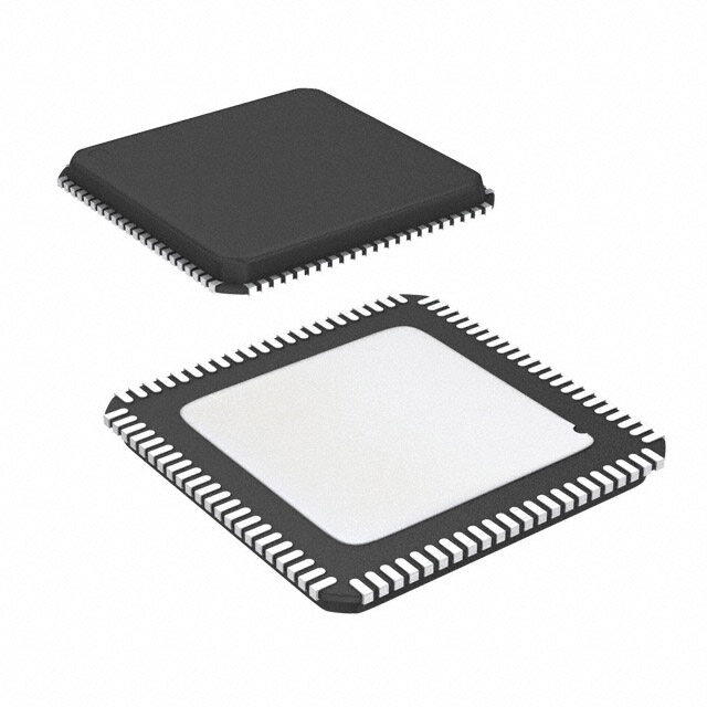
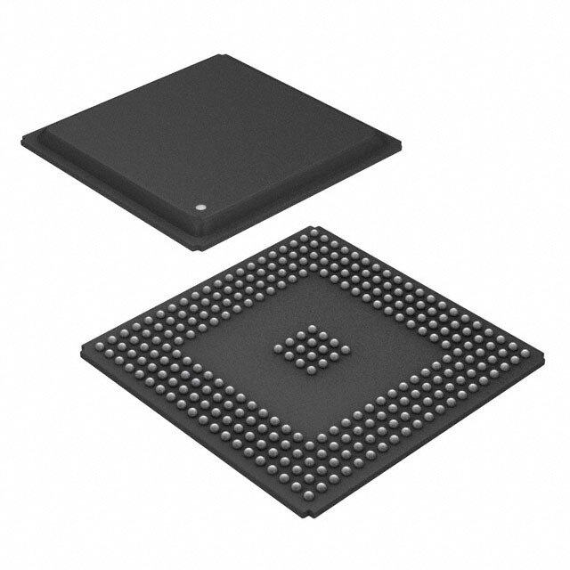
CY8C20xx7/S 48-pin QFN (31 Sensing Inputs)[31] Table 6. Pin Definitions – CY8C20637, CY8C20647/S, CY8C20667/S [32] n Figure 7. CY8C20637, CY8C20647/S, CY8C20667/S Device o Pin No. Digital Analog Name Descripti P0[1],AIVssP0[3],AINC,P0[7],AINCNCVddP0[6],AIP0[4],AIP0[2],AIP0[0],AI 1 NC No connection 87 6543210987 2 I/O I P2[7] NC 144444444433336 NC 3 I/O I P2[5] Crystal output (XOut) AI,P 2[7] 2 35 P2[4], AI 4 I/O I P2[3] Crystal input (XIn) AI, XOut,P 2[5] 3 34 P2[2], AI 5 I/O I P2[1] AI, XIn,P 2[3] 4 33 P2[0], AI 6 I/O I P4[3] AI,P 2[1] 5 32 P4[2], AI 7 I/O I P4[1] AI,P 4[3] 6 QFN 31 P4[0], AI 8 I/O I P3[7] AI,P 4[1] 7 (Top View) 30 P3[6], AI AI, P3[7] 8 29 P3[4], AI 9 I/O I P3[5] AI,P 3[5] 9 28 P3[2], AI 10 I/O I P3[3] AI,P 3[3] 10 27 P3[0], AI 11 I/O I P3[1] AI P3[1] 11 26 XRES 1123 IIOOHHRR II PP11[[75]] II22CC SSDCAL,, SSPPII SMSISO AI,I 2C SCL, SPI SS, P1[7] 1213141516171819202122232425 P1[6], AI 1111145678 IIOOHHPRRowerII NNPPV11SCCS[[31]] NNGSISPoorSo Icc PuCoon CnnLdnnKL ceeKocc[n3ttii3noo]e,nn cI2tCio nS[3C6L], SPI MOSI SPIMISO,AI,P1[5]NCNCSPICLK,AI,P1[3]CL,SPIMOSI,P1[1]VssNCNCVddKSDA,SPICL,P1[0]AI,P1[2]AI,EXTCLK,P1[4] 122222901234 IIIOOOHHHPRRRowerIII NNVPPP1D11CC[[[D240]]] DNNOSISuroopSipv tcciPepooo nlnDynn a SnnAvl eeThoeccAilxettta[iitl3ooedg3nnr e]On, Iau2lCt pc luSotDc (kAo pi,n StpioPunIt a Cl)LK[34] I2CSDA, KAIISSP CL,I2CS, ,I2CAI,ISSP DATA1 (EXTCLK) 25 IOHR I P1[6] 26 Input XRES Active high external reset with internal pull-down[35] 27 I/O I P3[0] 28 I/O I P3[2] 29 I/O I P3[4] n o Pin No. Digital Analog Name scripti e D 30 I/O I P3[6] 40 IOH I P0[6] 31 I/O I P4[0] 41 Power V Supply voltage DD 32 I/O I P4[2] 42 NC No connection 33 I/O I P2[0] 43 NC No connection 34 I/O I P2[2] Driven Shield Output (optional) 44 IOH I P0[7] 35 I/O I P2[4] Driven Shield Output (optional) 45 NC No connection 36 NC No connection 46 IOH I P0[3] Integrating input 37 IOH I P0[0] Driven Shield Output (optional) 47 Power V Ground connection[36 SS 38 IOH I P0[2] Driven Shield Output (optional) 48 IOH I P0[1] Integrating input 39 IOH I P0[4] CP Power V Center pad must be connected to ground SS LEGENDA = Analog, I = Input, O = Output, NC = No Connection H = 5 mA High Output Drive, R = Regulated Output. Notes 31.The center pad (CP) on the QFN package must be connected to ground (VSS) for best mechanical, thermal, and electrical performance. If not connected to ground, it must be electrically floated and not connected to any other signal. 32.34 GPIOs = 31 pins for capacitive sensing+2 pins for I2C + 1 pin for modulator capacitor. 33.On Power-up, the SDA(P1[0]) drives a strong high for 256 sleep clock cycles and drives resistive low for the next 256 sleep clock cycles. The SCL(P1[1]) line drives resistive low for 512 sleep clock cycles and both the pins transition to High impedance state. On reset, after XRES de- asserts, the SDA and the SCL lines drive resistive low for 8 sleep clock cycles and transition to high impedance state. In both cases, a pull-up resistance on these lines combines with the pull-down resistance (5.6K ohm) and form a potential divider. Hence, during power-up or reset event, P1[1] and P1[0] may disturb the I2C bus. Use alternate pins if you encounter issues. 34.Alternate SPI clock. 35.The internal pull down is 5KOhm. 36.All VSS pins should be brought out to one common GND plane. Document Number: 001-69257 Rev. *Q Page 12 of 46
CY8C20xx7/S Electrical Specifications This section presents the DC and AC electrical specifications of the CY8C20x37/47/67/S PSoC devices. For the latest electrical specifications, confirm that you have the most recent datasheet by visiting the web at http://www.cypress.com/psoc. Figure 8. Voltage versus CPU Frequency 5.5V Voltage OVaplierRdaetiginogn D D V 1.71V 750 kHz 3 MHz 24 MHz CPU Frequency Absolute Maximum Ratings Exceeding maximum ratings may shorten the useful life of the device. User guidelines are not tested. Table 7. Absolute Maximum Ratings Symbol Description Conditions Min Typ Max Units Higher storage temperatures reduce data retention time. Recommended Storage T Storage temperature Temperature is +25 °C ± 25 °C. Extended –55 +25 +125 °C STG duration storage temperatures above 85 °C degrades reliability. V Supply voltage relative to V – –0.5 – +6.0 V DD SS V DC input voltage – V – 0.5 – V + 0.5 V IO SS DD V DC voltage applied to tristate – V – 0.5 – V + 0.5 V IOZ SS DD I Maximum current into any port pin – –25 – +50 mA MIO ESD Electro static discharge voltage Human body model ESD 2000 – – V LU Latch up current In accordance with JESD78 standard – – 200 mA Operating Temperature Table 8. Operating Temperature Symbol Description Conditions Min Typ Max Units T Ambient temperature – –40 – +85 °C A T Commercial temperature range – 0 70 °C C The temperature rise from ambient to junction is package specific. See the Thermal Imped- T Operational die temperature ances on page 31. The user must limit the –40 – +100 °C J power consumption to comply with this requirement. Document Number: 001-69257 Rev. *Q Page 13 of 46
CY8C20xx7/S DC Chip-Level Specifications Table9 lists guaranteed maximum and minimum specifications for the entire voltage and temperature ranges. Table 9. DC Chip-Level Specifications Symbol Description Conditions Min Typ Max Units V [37, 38, 39] Supply voltage See Table14 on page17. 1.71 – 5.50 V DD Conditions are V 3.0 V, T = 25 °C, DD A I Supply current, IMO = 24 MHz CPU = 24 MHz. CapSense running at 12 MHz, – 2.88 4.00 mA DD24 no I/O sourcing current Conditions are V 3.0 V, T = 25 °C, DD A I Supply current, IMO = 12 MHz CPU = 12 MHz. CapSense running at – 1.71 2.60 mA DD12 12 MHz, no I/O sourcing current Conditions are V 3.0 V, T = 25 °C, DD A I Supply current, IMO = 6 MHz CPU = 6 MHz. CapSense running at 6 MHz, – 1.16 1.80 mA DD6 no I/O sourcing current I [40, 41, 42, 43] Deep sleep current V 3.0 V, T = 25 °C, I/O regulator turned off – 0.10 1.1 A SB0 DD A I [40, 41, 42, 43] Standby current with POR, LVD V 3.0 V, T = 25 °C, I/O regulator turned off – 1.07 1.50 A SB1 and sleep timer DD A I [40, 41, 42, 43] Standby current with I2C Conditions are VDD = 3.3 V, TA = 25 °C and – 1.64 – A SBI2C enabled CPU = 24 MHz Notes 37.When VDD remains in the range from 1.71 V to 1.9 V for more than 50 µs, the slew rate when moving from the 1.71 V to 1.9 V range to greater than 2 V must be slower than 1 V/500 µs to avoid triggering POR. The only other restriction on slew rates for any other voltage range or transition is the SRPOWER_UP parameter. 38. If powering down in standby sleep mode, to properly detect and recover from a VDD brown out condition any of the following actions must be taken: a. Bring the device out of sleep before powering down. b. Assure that VDD falls below 100 mV before powering back up. c. Set the No Buzz bit in the OSC_CR0 register to keep the voltage monitoring circuit powered during sleep. d. Increase the buzz rate to assure that the falling edge of VDD is captured. The rate is configured through the PSSDC bits in the SLP_CFG register. For the referenced registers, refer to the Technical Reference Manual. In deep sleep/standby sleep mode, additional low power voltage monitoring circuitry allows VDD brown out conditions to be detected and resets the device when VDD goes lower than 1.1 V at edge rates slower than 1 V/ms. 39.For proper CapSense block functionality, if the drop in VDD exceeds 5% of the base VDD, the rate at which VDD drops should not exceed 200 mV/s. Base VDD can be between 1.8 V and 5.5 V. 40.Errata: When programmable timer 0 is used in “one-shot” mode by setting bit 1 of register 0,B0h (PT0_CFG), and the timer interrupt is used to wake the device from sleep, the interrupt service routine (ISR) may be executed twice. For more information, see the “Errata” on page38. 41.Errata: When in sleep mode, if a GPIO interrupt happens simultaneously with a Timer0 or Sleep Timer interrupt, the GPIO interrupt may be missed, and the corresponding GPIO ISR not run. For more information, see the “Errata” on page38. 42.Errata: If an interrupt is posted a short time (within 2.5 CPU cycles) before firmware commands the device to sleep, the interrupt will be missed. For more information, see the “Errata” on page38. 43.Errata: Device wakes up from sleep when an analog interrupt is trigger. For more information, see the “Errata” on page38. Document Number: 001-69257 Rev. *Q Page 14 of 46
CY8C20xx7/S DC GPIO Specifications The following tables list guaranteed maximum and minimum specifications for the voltage and temperature ranges: 3.0 V to 5.5 V and –40 °C T 85 °C, 2.4 V to 3.0 V and –40 °C T 85 °C, or 1.71 V to 2.4 V and –40 °C T 85 °C, respectively. Typical A A A parameters apply to 5 V and 3.3 V at 25 °C and are for design guidance only. Table 10. 3.0 V to 5.5 V DC GPIO Specifications Symbol Description Conditions Min Typ Max Units R Pull-up resistor – 4 5.60 8 k PU High output voltage I < 10 A, maximum of 10 mA source V OH V – 0.20 – – V OH1 Port 2 or 3 pins current in all I/Os DD High output voltage I = 1 mA, maximum of 20 mA source V OH V – 0.90 – – V OH2 Port 2 or 3 Pins current in all I/Os DD High output voltage I < 10 A, maximum of 10 mA source V Port 0 or 1 pins with LDO regulator Disabled OH V – 0.20 – – V OH3 current in all I/Os DD for port 1 High output voltage I = 5 mA, maximum of 20 mA source V Port 0 or 1 pins with LDO regulator Disabled OH V – 0.90 – – V OH4 current in all I/Os DD for port 1 High output voltage I < 10 A, V > 3.1 V, maximum of V Port 1 Pins with LDO Regulator Enabled for OH DD 2.85 3.00 3.30 V OH5 4 I/Os all sourcing 5 mA 3 V out High output voltage I = 5 mA, V > 3.1 V, maximum of V Port 1 pins with LDO regulator enabled for 3 OH DD 2.20 – – V OH6 20mA source current in all I/Os V out High output voltage I < 10 A, V > 2.7 V, maximum of V OH DD 2.35 2.50 2.75 V OH7 Port 1 pins with LDO enabled for 2.5 V out 20mA source current in all I/Os High output voltage I = 2 mA, V > 2.7 V, maximum of V OH DD 1.90 – – V OH8 Port 1 pins with LDO enabled for 2.5 V out 20mA source current in all I/Os High output voltage I < 10 A, V > 2.7 V, maximum of V OH DD 1.60 1.80 2.10 V OH9 Port 1 pins with LDO enabled for 1.8 V out 20mA source current in all I/Os High output voltage I = 1 mA, V > 2.7 V, maximum of V OH DD 1.20 – – V OH10 Port 1 pins with LDO enabled for 1.8 V out 20mA source current in all I/Os I = 25 mA, V > 3.3 V, maximum of OL DD 60mA sink current on even port pins (for V Low output voltage example, P0[2] and P1[4]) and 60 mA sink – – 0.75 V OL current on odd port pins (for example, P0[3] and P1[5]) V Input low voltage – – – 0.80 V IL V Input high voltage – V × 0.65 – V + 0.7 V IH DD DD V Input hysteresis voltage – – 80 – mV H I Input leakage (Absolute Value) – – 0.001 1 A IL C Pin capacitance Package and pin dependent Temp = 25 °C 0.50 1.70 7 pF PIN Input Low Voltage with low threshold enable Bit3 of IO_CFG1 set to enable low VILLVT3.3 set, Enable for Port1 [44] threshold voltage of Port1 input 0.8 V – – Input High Voltage with low threshold enable Bit3 of IO_CFG1 set to enable low V 1.4 – – V IHLVT3.3 set, Enable for Port1 threshold voltage of Port1 input Input Low Voltage with low threshold enable Bit3 of IO_CFG1 set to enable low V 0.8 V – – ILLVT5.5 set, Enable for Port1 threshold voltage of Port1 input Input High Voltage with low threshold enable Bit3 of IO_CFG1 set to enable low V 1.7 – – V IHLVT5.5 set, Enable for Port1 threshold voltage of Port1 input Note 44.Errata: Pull-up resistor on port1 pins cannot be connected to a voltage that is greater than 0.7 V higher than CY8C20xx7/S VDD. For more information see item #7 in “Errata” on page38. Document Number: 001-69257 Rev. *Q Page 15 of 46
CY8C20xx7/S Table 11. 2.4 V to 3.0 V DC GPIO Specifications Symbol Description Conditions Min Typ Max Units R Pull-up resistor – 4 5.60 8 k PU High output voltage I < 10 A, maximum of 10 mA source V OH V - 0.20 – – V OH1 Port 2 or 3 pins current in all I/Os DD High output voltage I = 0.2 mA, maximum of 10 mA V OH V - 0.40 – – V OH2 Port 2 or 3 Pins source current in all I/Os DD High output voltage I < 10 A, maximum of 10 mA source V Port 0 or 1 pins with LDO regulator OH V - 0.20 – – V OH3 current in all I/Os DD Disabled for port 1 High output voltage I = 2 mA, maximum of 10 mA source V Port 0 or 1 pins with LDO regulator OH V - 0.50 – – V OH4 current in all I/Os DD Disabled for Port 1 High output voltage I < 10 A, V > 2.4 V, maximum of V Port 1 pins with LDO enabled for 1.8 V OH DD 1.50 1.80 2.10 V OH5A 20 mA source current in all I/Os out High output voltage I = 1 mA, V > 2.4 V, maximum of V Port 1 pins with LDO enabled for 1.8 V OH DD 1.20 – – V OH6A 20 mA source current in all I/Os out I = 10 mA, maximum of 30 mA sink OL current on even port pins (for example, V Low output voltage P0[2] and P1[4]) and 30 mA sink – – 0.75 V OL current on odd port pins (for example, P0[3] and P1[5]) V Input low voltage – – – 0.72 V IL V Input high voltage – V × 0.65 – V + 0.7 V IH DD DD V Input hysteresis voltage – – 80 – mV H I Input leakage (absolute value) – – 1 1000 nA IL Package and pin dependent C Capacitive load on pins 0.50 1.70 7 pF PIN Temp = 25 C Input Low Voltage with low threshold Bit3 of IO_CFG1 set to enable low V 0.7 V – ILLVT2.5 enable set, Enable for Port1 threshold voltage of Port1 input Input High Voltage with low threshold Bit3 of IO_CFG1 set to enable low V 1.2 – V IHLVT2.5 enable set, Enable for Port1 threshold voltage of Port1 input Table 12. 1.71 V to 2.4 V DC GPIO Specifications Symbol Description Conditions Min Typ Max Units R Pull-up resistor – 4 5.60 8 k PU High output voltage I = 10A, maximum of 10mA V OH V – 0.20 – – V OH1 Port 2 or 3 pins source current in all I/Os DD High output voltage I = 0.5mA, maximum of 10mA V OH V – 0.50 – – V OH2 Port 2 or 3 pins source current in all I/Os DD High output voltage I = 100A, maximum of 10mA V Port 0 or 1 pins with LDO regulator OH V – 0.20 – – V OH3 source current in all I/Os DD Disabled for Port 1 High output voltage I = 2mA, maximum of 10mA source V Port 0 or 1 Pins with LDO Regulator OH V – 0.50 – – V OH4 current in all I/Os DD Disabled for Port 1 Document Number: 001-69257 Rev. *Q Page 16 of 46
CY8C20xx7/S Table 12. 1.71 V to 2.4 V DC GPIO Specifications (continued) Symbol Description Conditions Min Typ Max Units I = 5 mA, maximum of 20 mA sink OL current on even port pins (for example, V Low output voltage P0[2] and P1[4]) and 30 mA sink – – 0.40 V OL current on odd port pins (for example, P0[3] and P1[5]) V Input low voltage – – – 0.30 × V V IL DD V Input high voltage – 0.65 × V – – V IH DD V Input hysteresis voltage – – 80 – mV H I Input leakage (absolute value) – – 1 1000 nA IL Package and pin dependent C Capacitive load on pins 0.50 1.70 7 pF PIN temp = 25 C Table 13. GPIO Current Sink and Source Specifications Supply Port 0/1 per I/O Port 2/3/4 per Total Current Even Total Current Odd Mode Units Voltage (max) I/O (max) Pins (max) Pins (max) Sink 5 5 20 30 mA 1.71–2.4 Source 2 0.5 10[45] mA Sink 10 10 30 30 mA 2.4–3.0 Source 2 0.2 10[45] mA Sink 25 25 60 60 mA 3.0–5.0 Source 5 1 20[45] mA DC Analog Mux Bus Specifications Table14 lists guaranteed maximum and minimum specifications for the entire voltage and temperature ranges. Table 14. DC Analog Mux Bus Specifications Symbol Description Conditions Min Typ Max Units Switch resistance to common analog R – – – 800 SW bus Resistance of initialization switch to R – – – 800 GND V SS The maximum pin voltage for measuring RSW and RGND is 1.8 V DC Low Power Comparator Specifications Table15 lists guaranteed maximum and minimum specifications for the entire voltage and temperature ranges. Table 15. DC Comparator Specifications Symbol Description Conditions Min Typ Max Units Low power comparator (LPC) common V Maximum voltage limited to V 0.2 – 1.8 V LPC mode DD I LPC supply current – – 10 80 A LPC V LPC voltage offset – – 2.5 30 mV OSLPC Note 45.Total current (odd + even ports) Document Number: 001-69257 Rev. *Q Page 17 of 46
CY8C20xx7/S Comparator User Module Electrical Specifications Table16 lists the guaranteed maximum and minimum specifications. Unless stated otherwise, the specifications are for the entire device voltage and temperature operating range: –40 °C TA 85 °C, 1.71 V V 5.5 V. DD Table 16. Comparator User Module Electrical Specifications Symbol Description Conditions Min Typ Max Units T Comparator response time 50 mV overdrive – 70 100 ns COMP Offset – Valid from 0.2 V to 1.5V – 2.5 30 mV Average DC current, 50 mV Current – – 20 80 µA overdrive Supply voltage > 2 V Power supply rejection ratio – 80 – dB PSRR Supply voltage < 2 V Power supply rejection ratio – 40 – dB Input range – – 0.2 1.5 V ADC Electrical Specifications Table 17. ADC User Module Electrical Specifications Symbol Description Conditions Min Typ Max Units Input V Input voltage range – 0 – VREFADC V IN C Input capacitance – – – 5 pF IIN Equivalent switched cap input 1/(500fF × 1/(400fF × 1/(300fF × R Input resistance resistance for 8-, 9-, or 10-bit IN data clock) data clock) data clock) resolution Reference V ADC reference voltage – 1.14 – 1.26 V REFADC Conversion Rate Source is chip’s internal main oscillator. See AC Chip-Level F Data clock 2.25 – 6 MHz CLK Specifications on page 21 for accuracy Data clock set to 6 MHz. S8 8-bit sample rate sample rate = 0.001/ – 23.43 – ksps (2^Resolution/Data Clock) Data clock set to 6 MHz. S10 10-bit sample rate sample rate = 0.001/ – 5.85 – ksps (2^resolution/data clock) DC Accuracy RES Resolution Can be set to 8, 9, or 10 bit 8 – 10 bits DNL Differential nonlinearity – –1 – +2 LSB INL Integral nonlinearity – –2 – +2 LSB 8-bit resolution 0 3.20 19.20 LSB E Offset error OFFSET 10-bit resolution 0 12.80 76.80 LSB E Gain error For any resolution –5 – +5 %FSR GAIN Power I Operating current – – 2.10 2.60 mA ADC PSRR (V > 3.0 V) – 24 – dB DD PSRR Power supply rejection ratio PSRR (V < 3.0 V) – 30 – dB DD Document Number: 001-69257 Rev. *Q Page 18 of 46
CY8C20xx7/S DC POR and LVD Specifications Table18 lists guaranteed maximum and minimum specifications for the entire voltage and temperature ranges. Table 18. DC POR and LVD Specifications Symbol Description Conditions Min Typ Max Units V 1.66 V selected in PSoC Designer 1.61 1.66 1.71 V POR0 VPOR1 2.36 V selected in PSoC Designer VDD must be greater than or equal to 1.71V – 2.36 2.41 V during startup, reset from the XRES pin, or VPOR2 2.60 V selected in PSoC Designer reset from watchdog. – 2.60 2.66 V V 2.82 V selected in PSoC Designer – 2.82 2.95 V POR3 V 2.45 V selected in PSoC Designer 2.40 2.45 2.51 V LVD0 V 2.71 V selected in PSoC Designer 2.64[46] 2.71 2.78 V LVD1 V 2.92 V selected in PSoC Designer 2.85[47] 2.92 2.99 V LVD2 V 3.02 V selected in PSoC Designer 2.95[48] 3.02 3.09 V LVD3 – V 3.13 V selected in PSoC Designer 3.06 3.13 3.20 V LVD4 V 1.90 V selected in PSoC Designer 1.84 1.90 2.32 V LVD5 V 1.80 V selected in PSoC Designer 1.75[49] 1.80 1.84 V LVD6 V 4.73 V selected in PSoC Designer 4.62 4.73 4.83 V LVD7 DC Programming Specifications Table19 lists guaranteed maximum and minimum specifications for the entire voltage and temperature ranges. Table 19. DC Programming Specifications Symbol Description Conditions Min Typ Max Units Supply voltage for flash write V – 1.71 – 5.25 V DDIWRITE operations Supply current during I – – 5 25 mA DDP programming or verify Input low voltage during See appropriate “DC GPIO Specifica- V – – V V ILP programming or verify tions” on page15 IL Input high voltage during See appropriate “DC GPIO Specifica- V V – – V IHP programming or verify tions” on page15 IH Input current when Applying V ILP I to P1[0] or P1[1] during Driving internal pull-down resistor – – 0.2 mA ILP programming or verify Input current when applying V IHP I to P1[0] or P1[1] during Driving internal pull-down resistor – – 1.5 mA IHP programming or verify Output low voltage during V – – – V + 0.75 V OLP programming or verify SS See appropriate “DC GPIO Specifica- Output high voltage during V tions” on page15. For V > 3V use V V – V V OHP programming or verify DD OH4 OH DD in Table10 on page15. Flash Flash write endurance Erase/write cycles per block 50,000 – – – ENPB Following maximum Flash write cycles; Flash Flash data retention 20 – – Years DR ambient temperature of 55 °C Notes 46.Always greater than 50 mV above VPPOR1 voltage for falling supply. 47.Always greater than 50 mV above VPPOR2 voltage for falling supply. 48.Always greater than 50 mV above VPPOR3 voltage for falling supply. 49.Always greater than 50 mV above VPPOR0 voltage for falling supply. Document Number: 001-69257 Rev. *Q Page 19 of 46
CY8C20xx7/S DC I2C Specifications Table20 list guaranteed maximum and minimum specifications for the voltage and temperature ranges: 3.0 V to 5.5 V and –40 °C T 85 °C, 2.4 V to 3.0 V and –40 °C T 85 °C, or 1.71 V to 2.4 V and –40 °C T 85 °C, respectively. Typical parameters apply A A A to 5 V and 3.3 V at 25 °C and are for design guidance only. Table 20. DC I2C Specifications[50] Symbol Description Conditions Min Typ Max Units 3.1 V ≤ V ≤ 5.5 V – – 0.25 × V V DD DD V Input low level 2.5 V ≤ V ≤ 3.0 V – – 0.3 × V V ILI2C DD DD 1.71 V ≤ V ≤ 2.4 V – – 0.3 × V V DD DD V + VIHI2C Input high level 1.71 V ≤ VDD ≤ 5.5 V 0.65 × VDD – 0.7DVD[51] V Shield Driver DC Specifications Table21 list guaranteed maximum and minimum specifications for the voltage and temperature ranges: 3.0 V to 5.5 V and –40 °C T 85 °C, 2.4 V to 3.0 V and –40 °C T 85 °C, or 1.71 V to 2.4 V and –40 °C T 85 °C, respectively. Typical parameters apply A A A to 5 V and 3.3 V at 25 °C and are for design guidance only. Table 21. Shield Driver DC Specifications Symbol Description Conditions Min Typ Max Units V Reference buffer output 1.7 V ≤ V ≤ 5.5 V 0.942 – 1.106 V Ref DD V Reference buffer output 1.7 V ≤ V ≤ 5.5 V 1.104 – 1.296 V RefHi DD DC IDAC Specifications Table22 lists guaranteed maximum and minimum specifications for the entire voltage and temperature ranges. Table 22. DC IDAC Specifications (8-bit IDAC) Symbol Description Min Typ Max Units Notes IDAC_DNL Differential nonlinearity –1 – 1 LSB – IDAC_INL Integral nonlinearity –2 – 2 LSB – Range = 4x 138 – 169 µA DAC setting = 127 dec IDAC_Current Range = 8x 138 – 169 µA DAC setting = 64 dec Table 23. DC IDAC Specifications (7-bit IDAC) Symbol Description Min Typ Max Units Notes IDAC_DNL Differential nonlinearity –1 – 1 LSB – IDAC_INL Integral nonlinearity –2 – 2 LSB – Range = 4x 137 – 168 µA DAC setting = 127 dec IDAC_Current Range = 8x 138 – 169 µA DAC setting = 64 dec Notes 50.Errata: Pull-up resistors on I2C interface cannot be connected to a supply voltage that is more than 0.7V higher than the CY8C20xx7/S power supply. For more information see item #6 in the “Errata” on page38. 51.Errata: For more information see item #6 in the “Errata” on page38. Document Number: 001-69257 Rev. *Q Page 20 of 46
CY8C20xx7/S AC Chip-Level Specifications Table24 lists guaranteed maximum and minimum specifications for the entire voltage and temperature ranges. Table 24. AC Chip-Level Specifications Symbol Description Conditions Min Typ Max Units F IMO frequency at 24 MHz Setting – 22.8 24 25.2 MHz IMO24 F IMO frequency at 12 MHz setting – 11.4 12 12.6 MHz IMO12 F IMO frequency at 6 MHz setting – 5.7 6.0 6.3 MHz IMO6 F CPU frequency – 0.75 – 25.20 MHz CPU F ILO frequency – 15 32 50 kHz 32K1 F ILO untrimmed frequency – – 32 – kHz 32K_U DC Duty cycle of IMO – 40 50 60 % IMO DC ILO duty cycle – 40 50 60 % ILO SR Power supply slew rate V slew rate during power-up – – 250 V/ms POWER_UP DD t External reset pulse width at power-up After supply voltage is valid 1 – – ms XRST t External reset pulse width after power-up[52] Applies after part has booted 10 – – s XRST2 6 MHz IMO cycle-to-cycle jitter (RMS) – – 0.7 6.7 ns 6 MHz IMO long term N cycle-to-cycle jitter – – 4.3 29.3 ns (RMS); N = 32 6 MHz IMO period jitter (RMS) – – 0.7 3.3 ns 12 MHz IMO cycle-to-cycle jitter (RMS) – – 0.5 5.2 ns t [53] 12 MHz IMO long term N cycle-to-cycle jitter – –– 2.3 5.6 ns JIT_IMO (RMS); N = 32 12 MHz IMO period jitter (RMS) – – 0.4 2.6 ns 24 MHz IMO cycle-to-cycle jitter (RMS) – – 1.0 8.7 ns 24 MHz IMO long term N cycle-to-cycle jitter – – 1.4 6.0 ns (RMS); N = 32 24 MHz IMO period jitter (RMS) – – 0.6 4.0 ns Note 52.The minimum required XRES pulse length is longer when programming the device (see Table28 on page23). 53.See the Cypress Jitter Specifications application note, Understanding Datasheet Jitter Specifications for Cypress Timing Products – AN5054 for more information. Document Number: 001-69257 Rev. *Q Page 21 of 46
CY8C20xx7/S AC General Purpose I/O Specifications Table25 lists guaranteed maximum and minimum specifications for the entire voltage and temperature ranges. Table 25. AC GPIO Specifications Symbol Description Conditions Min Typ Max Units 6 MHz for 0 – MHz 1.71 V <V < 2.40 V F GPIO operating frequency Normal strong mode Port 0, 1 DD GPIO 12 MHz for 0 – MHz 2.40 V < V < 5.50 V DD Rise time, strong mode, Cload = 50 pF t V = 3.0 to 3.6 V, 10% to 90% 15 – 80 ns RISE23 Ports 2 or 3 DD Rise time, strong mode low supply, t V = 1.71 to 3.0 V, 10% to 90% 15 – 80 ns RISE23L Cload = 50 pF, Ports 2 or 3 DD Rise time, strong mode, Cload = 50 pF V = 3.0 to 3.6 V, 10% to 90% t DD 10 – 50 ns RISE01 Ports 0 or 1 LDO enabled or disabled Rise time, strong mode low supply, V = 1.71 to 3.0 V, 10% to 90% t DD 10 – 80 ns RISE01L Cload = 50 pF, Ports 0 or 1 LDO enabled or disabled Fall time, strong mode, Cload = 50 pF t V = 3.0 to 3.6 V, 10% to 90% 10 – 50 ns FALL all ports DD Fall time, strong mode low supply, t V = 1.71 to 3.0 V, 10% to 90% 10 – 70 ns FALLL Cload = 50 pF, all ports DD Figure 9. GPIO Timing Diagram 90% GPIO Pin Output Voltage 10% TRise23 TFall TRise01 TFallL TRise23L TRise01L AC Comparator Specifications Table26 lists guaranteed maximum and minimum specifications for the entire voltage and temperature ranges. Table 26. AC Low Power Comparator Specifications Symbol Description Conditions Min Typ Max Units Comparator response time, 50 mV overdrive does not include t – – 100 ns LPC 50 mV overdrive offset voltage. AC External Clock Specifications Table27 lists guaranteed maximum and minimum specifications for the entire voltage and temperature ranges. Table 27. AC External Clock Specifications Symbol Description Conditions Min Typ Max Units Frequency (external oscillator – 0.75 – 25.20 MHz frequency) F High period – 20.60 – 5300 ns OSCEXT Low period – 20.60 – – ns Power-up IMO to switch – 150 – – s Document Number: 001-69257 Rev. *Q Page 22 of 46
CY8C20xx7/S AC Programming Specifications Figure 10. AC Waveform SCLK (P1[1]) TRSCLK TFSCLK SDATA (P1[0]) TSSCLK THSCLK TDSCLK Table28 lists the guaranteed maximum and minimum specifications for the entire voltage and temperature ranges. Table 28. AC Programming Specifications Symbol Description Conditions Min Typ Max Units t Rise time of SCLK – 1 – 20 ns RSCLK t Fall time of SCLK – 1 – 20 ns FSCLK t Data setup time to falling edge of SCLK – 40 – – ns SSCLK t Data hold time from falling edge of SCLK – 40 – – ns HSCLK F Frequency of SCLK – 0 – 8 MHz SCLK t Flash erase time (block) – – – 18 ms ERASEB t Flash block write time – – – 25 ms WRITE t Data out delay from falling edge of SCLK 3.6 V – – 60 ns DSCLK DD t Data out delay from falling edge of SCLK 3.0 V 3.6 – – 85 ns DSCLK3 DD t Data out delay from falling edge of SCLK 1.71 V 3.0 – – 130 ns DSCLK2 DD Required to enter programming t External reset pulse width after power-up 300 – – s XRST3 mode when coming out of sleep t XRES pulse length – 300 – – s XRES t [54] V stable to wait-and-poll hold off – 0.1 – 1 ms VDDWAIT DD t [54] V stable to XRES assertion delay – 14.27 – – ms VDDXRES DD t SDAT high pulse time – 0.01 – 200 ms POLL t [54] “Key window” time after a VDD ramp – 3.20 – 19.60 ms ACQ acquire event, based on 256 ILO clocks. t [54] “Key window” time after an XRES event, – 98 – 615 s XRESINI based on 8 ILO clocks Note 54.Valid from 5 to 50°C. See the spec, CY8C20X66, CY8C20X46, CY8C20X36, CY7C643XX, CY7C604XX, CY8CTST2XX, CY8CTMG2XX, CY8C20X67, CY8C20X47, CY8C20X37, Programming Spec for more details. Document Number: 001-69257 Rev. *Q Page 23 of 46
CY8C20xx7/S AC I2C Specifications Table29 lists guaranteed maximum and minimum specifications for the entire voltage and temperature ranges. Table 29. AC Characteristics of the I2C SDA and SCL Pins Standard Fast Mode Symbol Description Mode Units Min Max Min Max f SCL clock frequency 0 100 0 400 kHz SCL Hold time (repeated) START condition. After this period, the first clock pulse is t 4.0 – 0.6 – µs HD;STA generated t LOW period of the SCL clock 4.7 – 1.3 – µs LOW t HIGH Period of the SCL clock 4.0 – 0.6 – µs HIGH t Setup time for a repeated START condition 4.7 – 0.6 – µs SU;STA t [55] Data hold time 20 3.45 20 0.90 µs HD;DAT t Data setup time 250 – 100[56] – ns SU;DAT t Setup time for STOP condition 4.0 – 0.6 – µs SU;STO t Bus free time between a STOP and START condition 4.7 – 1.3 – µs BUF t Pulse width of spikes are suppressed by the input filter – – 0 50 ns SP Figure 11. Definition for Timing for Fast/Standard Mode on the I2C Bus Notes 55.Errata: To wake up from sleep using I2C hardware address match event, I2C interface needs 20ns hold time on SDA line with respect to falling edge of SCL. For more information see item #5 in the “Errata” on page38. 56.A Fast-Mode I2C-bus device can be used in a standard mode I2C-bus system, but the requirement tSU;DAT 250 ns must then be met. This automatically be the case if the device does not stretch the LOW period of the SCL signal. If such device does stretch the LOW period of the SCL signal, it must output the next data bit to the SDA line trmax + tSU;DAT = 1000 + 250 = 1250 ns (according to the Standard-Mode I2C-bus specification) before the SCL line is released. Document Number: 001-69257 Rev. *Q Page 24 of 46
CY8C20xx7/S Table 30. SPI Master AC Specifications Symbol Description Conditions Min Typ Max Units V 2.4 V – – 6 MHz F SCLK clock frequency DD SCLK V < 2.4 V – – 3 MHz DD DC SCLK duty cycle – – 50 – % V 2.4 V 60 – – ns t MISO to SCLK setup time DD SETUP V < 2.4 V 100 – – ns DD t SCLK to MISO hold time – 40 – – ns HOLD t SCLK to MOSI valid time – – – 40 ns OUT_VAL t MOSI high time – 40 – – ns OUT_H Figure 12. SPI Master Mode 0 and 2 SPI Master, modes 0 and 2 1/FSCLK TLOW THIGH SCLK (mode 0) SCLK (mode 2) TSETUP THOLD MISO MSB LSB (input) TOUT_SU TOUT_H MOSI (output) Figure 13. SPI Master Mode 1 and 3 SPI Master, modes 1 and 3 1/FSCLK THIGH TLOW SCLK (mode 1) SCLK (mode 3) TSETUP THOLD MISO MSB LSB (input) TOUT_SU TOUT_H MOSI MSB LSB (output) Document Number: 001-69257 Rev. *Q Page 25 of 46
CY8C20xx7/S Table 31. SPI Slave AC Specifications Symbol Description Conditions Min Typ Max Units F SCLK clock frequency – – – 4 MHz SCLK t SCLK low time – 42 – – ns LOW t SCLK high time – 42 – – ns HIGH t MOSI to SCLK setup time – 30 – – ns SETUP t SCLK to MOSI hold time – 50 – – ns HOLD t SS high to MISO valid – – – 153 ns SS_MISO t SCLK to MISO valid – – – 125 ns SCLK_MISO t SS high time – 50 – – ns SS_HIGH t Time from SS low to first SCLK – 2/SCLK – – ns SS_CLK t Time from last SCLK to SS high – 2/SCLK – – ns CLK_SS Figure 14. SPI Slave Mode 0 and 2 SPI Slave, modes 0 and 2 TSS_CLK TCLK_SS TSS_HIGH /SS 1/FSCLK TLOW THIGH SCLK (mode 0) SCLK (mode 2) TSS_MISO TOUT_H MISO (output) TSETUP THOLD MOSI (input) MSB LSB Figure 15. SPI Slave Mode 1 and 3 SPI Slave, modes 1 and 3 TSS_CLK TCLK_SS /SS 1/FSCLK THIGH TLOW SCLK (mode 1) SCLK (mode 3) TOUT_H TSS_MISO TSCLK_MISO MISO MSB LSB (output) TSETUP THOLD MOSI (input) MSB LSB Document Number: 001-69257 Rev. *Q Page 26 of 46
CY8C20xx7/S Packaging Information This section illustrates the packaging specifications for the CY8C20x37/47/67 PSoC device, along with the thermal impedances for each package. Important Note Emulation tools may require a larger area on the target PCB than the chip’s footprint. For a detailed description of the emulation tools’ dimensions, refer to the document titled PSoC Emulator Pod Dimensions at http://www.cypress.com/design/MR10161. Figure 16. 16-pin (150 Mil) SOIC 51-85068 *E Figure 17. 16-pin Chip-On-Lead (3 × 3 × 0.6 mm) (Sawn) Package Outline, 001-09116 001-09116 *J Document Number: 001-69257 Rev. *Q Page 27 of 46
CY8C20xx7/S Figure 18. 24-Pin (4 × 4 × 0.6 mm) QFN 001-13937 *G Document Number: 001-69257 Rev. *Q Page 28 of 46
CY8C20xx7/S Figure 19. 32-Pin (5 × 5 × 0.6 mm) QFN SEE NOTE 1 TOP VIEW BOTTOM VIEW SIDE VIEW NOTES: DIMENSIONS SYMBOL 1. HATCH AREA IS SOLDERABLE EXPOSED PAD MIN. NOM. MAX. 2. BASED ON REF JEDEC # MO-248 A 0.50 0.55 0.60 3. PACKAGE WEIGHT: 0.0388g A1 - 0.020 0.045 4. DIMENSIONS ARE IN MILLIMETERS A2 0.15 BSC D 4.90 5.00 5.10 D2 3.40 3.50 3.60 E 4.90 5.00 5.10 E2 3.40 3.50 3.60 L 0.30 0.40 0.50 b 0.18 0.25 0.30 001-42168 *F e 0.50 TYP Document Number: 001-69257 Rev. *Q Page 29 of 46
CY8C20xx7/S Figure 20. 48-Pin (6 × 6 × 0.6 mm) QFN 001-57280 *E Figure 21. 30-pin WLCSP 001-50669 *D Important Notes ■For information on the preferred dimensions for mounting QFN packages, see the following Application Note at http://www.amkor.com/products/notes_papers/MLFAppNote.pdf. ■Pinned vias for thermal conduction are not required for the low power PSoC device. Document Number: 001-69257 Rev. *Q Page 30 of 46
CY8C20xx7/S Thermal Impedances Table 32. Thermal Impedances per Package Package Typical [57] JA 16-pin SOIC 95 C/W 16-pin QFN 33 C/W 24-pin QFN[58] 21 C/W 32-pin QFN[58] 20 C/W 48-pin QFN[58] 18 C/W 30-ball WLCSP 54 C/W Capacitance on Crystal Pins Table 33. Typical Package Capacitance on Crystal Pins Package Package Capacitance 32-Pin QFN 3.2 pF 48-Pin QFN 3.3 pF Solder Reflow Peak Temperature Table34 shows the solder reflow temperature limits that must not be exceeded. Table 34. Solder Reflow Peak Temperature Package Maximum Peak Temperature (TC) Maximum Time above TC – 5 C 16-pin SOIC 260 C 30 seconds 16-pin QFN 260 C 30 seconds 24-pin QFN 260 C 30 seconds 32-pin QFN 260 C 30 seconds 48-pin QFN 260 C 30 seconds 30-ball WLCSP 260 C 30 seconds Notes 57.TJ = TA + Power × JA. 58.To achieve the thermal impedance specified for the QFN package, the center thermal pad must be soldered to the PCB ground plane. Document Number: 001-69257 Rev. *Q Page 31 of 46
CY8C20xx7/S Development Tool Selection PSoC Programmer PSoC Programmer is flexible enough and is used on the bench Software in development and is also suitable for factory programming. PSoC Programmer works either as a standalone programming PSoC Designer™ application or operates directly from PSoC Designer. PSoC At the core of the PSoC development software suite is Programmer software is compatible with both PSoC ICE Cube PSoCDesigner, used to generate PSoC firmware applications. in-circuit Emulator and PSoC MiniProg. PSoC programmer is PSoC Designer is a Microsoft® Windows-based, integrated available free of cost at development environment for the Programmable System-on- http://www.cypress.com/psocprogrammer. Chip (PSoC) devices. The PSoC Designer IDE and application runs on Windows XP and Windows Vista. Development Kits This system provides design database management by project, All development kits are sold at the Cypress Online Store. in-system programming support, and built-in support for third- Evaluation Tools party assemblers and C compilers. PSoC Designer also supports C language compilers developed specifically for the All evaluation tools are sold at the Cypress Online Store. devices in the PSoC family. PSoC Designer is available free of charge at CY3210-MiniProg1 http://www.cypress.com/psocdesigner and includes a free C The CY3210-MiniProg1 kit allows you to program PSoC devices compiler. through the MiniProg1 programming unit. The MiniProg is a small, compact prototyping programmer that connects to the PC PSoC Designer Software Subsystems through a provided USB 2.0 cable. The kit includes: You choose a base device to work with and then select different onboard analog and digital components called user modules that ■MiniProg programming unit use the PSoC blocks. Examples of user modules are ADCs, ■MiniEval socket programming and evaluation board DACs, Amplifiers, and Filters. You configure the user modules for your chosen application and connect them to each other and ■28-pin CY8C29466-24PXI PDIP PSoC device sample to the proper pins. Then you generate your project. This ■28-pin CY8C27443-24PXI PDIP PSoC device sample prepopulates your project with APIs and libraries that you can use to program your application. ■PSoC Designer software CD The tool also supports easy development of multiple ■Getting Started guide configurations and dynamic reconfiguration. Dynamic reconfiguration allows for changing configurations at run time. ■USB 2.0 cable Code Generation Tools PSoC Designer supports multiple third- party C compilers and assemblers. The code generation tools CY3210-PSoCEval1 work seamlessly within the PSoC Designer interface and have The CY3210-PSoCEval1 kit features an evaluation board and been tested with a full range of debugging tools. The choice is the MiniProg1 programming unit. The evaluation board includes yours. an LCD module, potentiometer, LEDs, and plenty of bread- boarding space to meet all of your evaluation needs. The kit Assemblers. The assemblers allow assembly code to be includes: merged seamlessly with C code. Link libraries automatically use absolute addressing or are compiled in relative mode, and linked ■Evaluation board with LCD module with other software modules to get absolute addressing. ■MiniProg programming unit C Language Compilers. C language compilers are available ■Two 28-pin CY8C29466-24PXI PDIP PSoC device samples that support the PSoC family of devices. The products allow you ■PSoC Designer software CD to create complete C programs for the PSoC family devices. The optimizing C compilers provide all the features of C tailored to ■Getting Started guide the PSoC architecture. They come complete with embedded ■USB 2.0 cable libraries providing port and bus operations, standard keypad and display support, and extended math functionality. Document Number: 001-69257 Rev. *Q Page 32 of 46
CY8C20xx7/S Device Programmers CY3207ISSP In-System Serial Programmer (ISSP) All device programmers are purchased from the Cypress Online The CY3207ISSP is a production programmer. It includes Store. protection circuitry and an industrial case that is more robust than the MiniProg in a production-programming environment. CY3216 Modular Programmer Note CY3207ISSP needs special software and is not compatible The CY3216 Modular Programmer kit features a modular with PSoC Programmer. The kit includes: programmer and the MiniProg1 programming unit. The modular programmer includes three programming module cards and ■CY3207 programmer unit supports multiple Cypress products. The kit includes: ■PSoC ISSP software CD ■Modular programmer base ■110 ~ 240 V power supply, Euro-Plug adapter ■Three programming module cards ■USB 2.0 cable ■MiniProg programming unit ■PSoC Designer software CD ■Getting Started guide ■USB 2.0 cable Third Party Tools Several tools have been specially designed by the following third-party vendors to accompany PSoC devices during development and production. Specific details for each of these tools can be found at http://www.cypress.com under Documentation > Evaluation Boards. Document Number: 001-69257 Rev. *Q Page 33 of 46
CY8C20xx7/S Ordering Information Table35 lists the CY8C20x37/47/67/S PSoC devices’ key package features and ordering codes. Table 35. PSoC Device Key Features and Ordering Information Flash SRAM CapSense Digital I/O Analog XRES Ordering Code Package ADC (Bytes) (Bytes) Sensors Pins Inputs [59] Pin CY8C20237-24SXI 16-pin SOIC 8 K 1 K 10 13 13 Yes Yes CY8C20247S-24SXI 16-pin SOIC 16 K 2 K 10 13 13 Yes Yes CY8C20237-24LKXI 16-pin QFN 8 K 1 K 10 13 13 Yes Yes CY8C20237-24LKXIT 16-pin QFN (Tape and Reel) 8 K 1 K 10 13 13 Yes Yes CY8C20247S-24LKXI 16-pin QFN 16 K 2 K 10 13 13 Yes Yes CY8C20247S-24LKXIT 16-pin QFN (Tape and Reel) 16 K 2 K 10 13 13 Yes Yes CY8C20337-24LQXI 24-pin QFN 8 K 1 K 16 19 19 Yes Yes CY8C20337-24LQXIT 24-pin QFN (Tape and Reel) 8 K 1 K 16 19 19 Yes Yes CY8C20347-24LQXI 24-pin QFN 16 K 2 K 16 19 19 Yes Yes CY8C20347-24LQXIT 24-pin QFN (Tape and Reel) 16 K 2 K 16 19 19 Yes Yes CY8C20347S-24LQXI 24-pin QFN 16 K 2 K 16 19 19 Yes Yes CY8C20347S-24LQXIT 24-pin QFN (Tape and Reel) 16 K 2 K 16 19 19 Yes Yes CY8C20437-24LQXI 32-pin QFN 8 K 1 K 25 28 28 Yes Yes CY8C20437-24LQXIT 32-pin QFN (Tape and Reel) 8 K 1 K 25 28 28 Yes Yes CY8C20447-24LQXI 32-pin QFN 16 K 2 K 25 28 28 Yes Yes CY8C20447-24LQXIT 32-pin QFN (Tape and Reel) 16 K 2 K 25 28 28 Yes Yes CY8C20447S-24LQXI 32-pin QFN 16 K 2 K 25 28 28 Yes Yes CY8C20447S-24LQXIT 32-pin QFN (Tape and Reel) 16 K 2 K 25 28 28 Yes Yes CY8C20467-24LQXI 32-pin QFN 32 K 2 K 25 28 28 Yes Yes CY8C20467-24LQXIT 32-pin QFN (Tape and Reel) 32 K 2 K 25 28 28 Yes Yes CY8C20467S-24LQXI 32-pin QFN 32 K 2 K 25 28 28 Yes Yes CY8C20467S-24LQXIT 32-pin QFN (Tape and Reel) 32 K 2 K 25 28 28 Yes Yes CY8C20637-24LQXI 48-pin QFN 8 K 1 K 31 34 34 Yes Yes CY8C20637-24LQXIT 48-pin QFN (Tape and Reel) 8 K 1 K 31 34 34 Yes Yes CY8C20647-24LQXI 48-pin QFN 16 K 2 K 31 34 34 Yes Yes CY8C20647-24LQXIT 48-pin QFN (Tape and Reel) 16 K 2 K 31 34 34 Yes Yes CY8C20647S-24LQXI 48-pin QFN 16 K 2 K 31 34 34 Yes Yes CY8C20647S-24LQXIT 48-pin QFN (Tape and Reel) 16 K 2 K 31 34 34 Yes Yes CY8C20667-24LQXI 48-pin QFN 32 K 2 K 31 34 34 Yes Yes CY8C20667-24LQXIT 48-pin QFN (Tape and Reel) 32 K 2 K 31 34 34 Yes Yes CY8C20667S-24LQXI 48-pin QFN 32 K 2 K 31 34 34 Yes Yes CY8C20667S-24LQXIT 48-pin QFN (Tape and Reel) 32 K 2 K 31 34 34 Yes Yes Note 59.Dual-function Digital I/O Pins also connect to the common analog mux. Document Number: 001-69257 Rev. *Q Page 34 of 46
CY8C20xx7/S Table 35. PSoC Device Key Features and Ordering Information (continued) Flash SRAM CapSense Digital I/O Analog XRES Ordering Code Package ADC (Bytes) (Bytes) Sensors Pins Inputs [59] Pin CY8C20767-24FDXC 30-pin WLCSP 32 K 2 K 24 27 27 Yes Yes CY8C20767-24FDXCT 30-pin WLCSP (Tape and Reel) 32 K 2 K 24 27 27 Yes Yes Ordering Code Definitions CY 8 C 20 XX7 X-24 XX X X (T) Tape and reel Temperature range: X = C or I C = Commercial; I = Industrial Pb-free Package Types: XX = S, LK, LQ, or FD S = 16-pin SOIC LK = 16-pin QFN (no center pad) LQ = 24-pin QFN, 32-pin QFN, 48-pin QFN FD = 30-ball WLCSP Speed grade = 24 MHz S = SmartSense™ Auto-tuning Enabled Part Number Family Code Technology Code: C = CMOS Marketing Code: 8 = PSoC Company ID: CY = Cypress Document Number: 001-69257 Rev. *Q Page 35 of 46
CY8C20xx7/S Acronyms The following table lists the acronyms that are used in this Reference Documents document. ■Technical reference manual for CY20xx7 devices Table 36. Acronyms Used in this Document ■In-system Serial Programming (ISSP) protocol for 20xx7 Acronym Description AC alternating current ■Host Sourced Serial Programming for 20xx7 devices ADC analog-to-digital converter Document Conventions API application programming interface CMOS complementary metal oxide semiconductor Units of Measure CPU central processing unit Table37 lists all the abbreviations used to measure the PSoC DAC digital-to-analog converter devices. DC direct current Table 37. Units of Measure ESD electrostatic discharge Symbol Unit of Measure FSR full scale range °C degree Celsius GPIO general purpose input/output dB decibel I2C inter-integrated circuit kHz kilohertz ICE in-circuit emulator ksps kilo samples per second ILO internal low speed oscillator k kilohm IMO internal main oscillator I/O input/output MHz megahertz ISSP in-system serial programming A microampere LCD liquid crystal display s microsecond LDO low dropout (regulator) mA milliampere LED light-emitting diode mm millimeter LPC low power comparator ms millisecond LSB least-significant bit mV millivolt LVD low voltage detect nA nanoampere MCU micro-controller unit ns nanosecond MIPS million instructions per second ohm MISO master in slave out % percent MOSI master out slave in pF picofarad MSB most-significant bit V volt OCD on-chip debug PCB printed circuit board W watt POR power on reset PSRR power supply rejection ratio PWRSYS power system PSoC programmable system-on-chip QFN quad flat no-lead SCLK serial I2C clock SDA serial I2C data SDATA serial ISSP data SOIC small outline integrated circuit SPI serial peripheral interface SRAM static random access memory SS slave select USB universal serial bus WLCSP wafer level chip scale package Document Number: 001-69257 Rev. *Q Page 36 of 46
CY8C20xx7/S Numeric Naming Hexadecimal numbers are represented with all letters in uppercase with an appended lowercase ‘h’ (for example, ‘14h’ or ‘3Ah’). Hexadecimal numbers may also be represented by a ‘0x’ prefix, the C coding convention. Binary numbers have an appended lowercase ‘b’ (for example, 01010100b’ or ‘01000011b’). Numbers not indicated by an ‘h’, ‘b’, or 0x are decimal. Glossary Crosspoint connection Connection between any GPIO combination via analog multiplexer bus. Differential non linearity Ideally, any two adjacent digital codes correspond to output analog voltages that are exactly one LSB apart. Differential non-linearity is a measure of the worst case deviation from the ideal 1 LSB step. Hold time Hold time is the time following a clock event during which the data input to a latch or flip- flop must remain stable in order to guarantee that the latched data is correct. I2C It is a serial multi-master bus used to connect low speed peripherals to MCU. Integral nonlinearity It is a term describing the maximum deviation between the ideal output of a DAC/ADC and the actual output level. Latch-up current Current at which the latch-up test is conducted according to JESD78 standard (at 125 degree Celsius) Power supply rejection ratio (PSRR) The PSRR is defined as the ratio of the change in supply voltage to the corresponding change in output voltage of the device. Scan The conversion of all sensor capacitances to digital values. Setup time Period required to prepare a device, machine, process, or system for it to be ready to function. Signal-to-noise ratio The ratio between a capacitive finger signal and system noise. SPI Serial peripheral interface is a synchronous serial data link standard. Document Number: 001-69257 Rev. *Q Page 37 of 46
CY8C20xx7/S Errata This section describes the errata for the CY8C20xx7/S family. Details include errata trigger conditions, scope of impact, available workaround, and silicon revision applicability. Contact your local Cypress Sales Representative if you have questions. CY8C20xx7/S Qualification Status Product Status: Production released. CY8C20xx7/S Errata Summary The following Errata items apply to the CY8C20xx7/S datasheet 001-69257. 1.DoubleTimer0 ISR ■Problem Definition When programmable timer 0 is used in “one-shot” mode by setting bit 1 of register 0,B0h (PT0_CFG), and the timer interrupt is used to wake the device from sleep, the interrupt service routine (ISR) may be executed twice. ■Parameters Affected No datasheet parameters are affected. ■Trigger Condition(S) Triggered by enabling one-shot mode in the timer, and using the timer to wake from sleep mode. ■Scope of Impact The ISR may be executed twice. ■Workaround In the ISR, firmware should clear the one-shot bit with a statement such as “and reg[B0h], FDh” ■Fix Status Will not be fixed ■Changes None 2.Missed GPIO Interrupt ■Problem Definition When in sleep mode, if a GPIO interrupt happens simultaneously with a Timer0 or Sleep Timer interrupt, the GPIO interrupt may be missed, and the corresponding GPIO ISR not run. ■Parameters Affected No datasheet parameters are affected. ■Trigger Condition(S) Triggered by enabling sleep mode, then having GPIO interrupt occur simultaneously with a Timer 0 or Sleep Timer interrupt. ■Scope of Impact The GPIO interrupt service routine will not be run. ■Workaround The system should be architected such that a missed GPIO interrupt may be detected. For example, if a GPIO is used to wake the system to perform some function, the system should detect if the function is not performed, and re-issue the GPIO interrupt. Alternatively, if a GPIO interrupt is required to wake the system, then firmware should disable the Sleep Timer and Timer0. Alternatively, the ISR’s for Sleep Timer and Timer0 should manually check the state of the GPIO to determine if the host system has attempted to generate a GPIO interrupt. ■Fix Status Will not be fixed ■Changes None Document Number: 001-69257 Rev. *Q Page 38 of 46
CY8C20xx7/S 3.Missed Interrupt During Transition to Sleep ■Problem Definition If an interrupt is posted a short time (within 2.5 CPU cycles) before firmware commands the device to sleep, the interrupt will be missed. ■Parameters Affected No datasheet parameters are affected. ■Trigger Condition(S) Triggered by enabling sleep mode just prior to an interrupt. ■Scope of Impact The relevant interrupt service routine will not be run. ■Workaround None. ■Fix Status Will not be fixed ■Changes None 4.Wakeup from sleep with analog interrupt ■Problem Definition Device wakes up from sleep when an analog interrupt is trigger ■Parameters Affected No datasheet parameters are affected. ■Trigger Condition(S) Triggered by enabling analog interrupt during sleep mode when device operating temperature is 50 °C or above ■Scope of Impact Device unexpectedly wakes up from sleep ■Workaround Disable the analog interrupt before entering sleep and turn it back on upon wake-up. ■Fix Status Will not be fixed ■Changes None Document Number: 001-69257 Rev. *Q Page 39 of 46
CY8C20xx7/S 5.Wake-up from Sleep with Hardware I2C Address match on Pins P1[0], P1[1] ■Problem Definition I2C interface needs 20 ns hold time on SDA line with respect to falling edge of SCL, to wake-up from sleep using I2C hardware address match event. ■Parameters Affected t increased to 20 ns from 0 ns HD;DAT ■Trigger Condition(S) This is an issue only when all these three conditions are met: 1) P1.0 and P1.1 are used as I2C pins, 2) Wakeup from sleep with hardware address match feature is enabled, and 3) I2C master does not provide 20 ns hold time on SDA with respect to falling edge of SCL. ■Scope of Impact These trigger conditions cause the device to never wake-up from sleep based on I2C address match event. ■Workaround For a design that meets all of the trigger conditions, the following suggested circuit has to be implemented as a work-around. The R and C values proposed are 100ohm and 200pF respectively. ■Fix Status Will not be fixed ■Changes None Document Number: 001-69257 Rev. *Q Page 40 of 46
CY8C20xx7/S 6.I2C Port Pin Pull-up Supply Voltage ■Problem Definition Pull-up resistor on I2C interface cannot be connected to a supply voltage that is greater than 0.7V of CY8C20xx7/S V . DD ■Parameters Affected None. ■Trigger Condition(S) This problem occurs only when the I2C master is powered at a higher voltage than CY8C20xx7/S. ■Scope of Impact This trigger condition will corrupt the I2C communication between the I2C host and the CY8C20xx7/S CapSense controller. ■Workaround I2C master cannot be powered at a supply voltage that is greater than 0.7V compared to CY8C20xx7/S supply voltage. ■Fix Status Will not be fixed ■Changes None 7.Port1 Pin Voltage ■Problem Definition Pull-up resistor on port1 pins cannot be connected to a voltage that is greater than 0.7V higher than CY8C20xx7/S V . DD ■Parameters Affected None. ■Trigger Condition(S) This problem occurs only when port1 pins are at voltage 0.7V higher than V of CY8C20xx7/S. DD ■Scope of Impact This trigger condition will not allow CY8C20xx7/S to drive the output signal on port1 pins, input path is unaffected by this condition. ■Workaround Port1 should not be connected to a higher voltage than V of CY8C20xx7/S. DD ■Fix Status Will not be fixed ■Changes None Document Number: 001-69257 Rev. *Q Page 41 of 46
CY8C20xx7/S Document History Page Document Title: CY8C20xx7/S, 1.8 V CapSense® Controller with SmartSense™ Auto-tuning 31 Buttons, 6 Sliders, Proximity Sensors Document Number: 001-69257 Orig. of Submission Revision ECN Description of Change Change Date ** 3276782 DST 06/27/2011 New silicon and document *A 3327230 DST 07/28/2011 Changed 48-pin dimensions to 6 × 6 × 0.6 mm QFN Updated pins name in Table3 on page9 and removed USB column and updated dimensions for 48-pin parts in Table35 on page34 Updated Figure 20 on page 30 Removed ICE and Debugger sections. Removed CY3215 Development Kit and CY3280-20x66 UCC sections. Updated Ordering Information. *B 3403111 YVA 10/12/2011 Moved status from Advance to Preliminary. Updated Ordering Information Removed the row named “48-Pin (6 × 6 mm) QFN (OCD)”. Changed all 48-pin ordering code column from CY8C20XXX-24LTxx to CY8C20XXX-24LQxx. Updated 16-pin SOIC and 16-pin QFN package drawings. *C 3473317 DST 12/23/2011 Updated Features. Updated Pinouts (Removed PSoC in captions of Figure2, Figure3, Figure4, Figure6, and Figure7). Updated DC Chip-Level Specifications under Electrical Specifications (Updated typical value of I parameter from 3.32 mA to 2.88 mA, updated DD24 typical value of I parameter from 1.86 mA to 1.71 mA, updated typical value DD12 of I parameter from 1.13 mA to 1.16 mA, updated maximum value of I DD6 SB0 parameter from 0.50 µA to 1.1 µA, added I parameter and its details). SBI2C Updated DC GPIO Specifications under Electrical Specifications (Added the parameters namely V V V V and their details in ILLVT3.3, IHLVT3.3, ILLVT5.5, IHLVT5.5 Table10, added the parameters namely V , V and their details in ILLVT2.5 IHLVT2.5 Table11). Added the following sections namely DC I2C Specifications, Shield Driver DC Specifications, and DC IDAC Specifications under Electrical Specifications. Updated AC Chip-Level Specifications (Added the parameter namely t JIT_IMO and its details). Updated Ordering Information (updated Table35). *D 3510277 YVA/DST 02/16/2012 Added CY8C20x37/37S/47/47S/67/67S part numbers and changed title to “1.8 V CapSense® Controller with SmartSense™ Auto-tuning 31 Buttons, 6 Sliders” Updated Features. Modified comparator blocks in Logic Block Diagram. Replaced SmartSense with SmartSense auto-tuning. Added CY8C20xx7S part numbers in Pin Definitions. Added footnote for Table20. Updated Table21 and Table22 and added Table23. Updated F min value. 32K1 Updated data hold time min values. Updated CY8C206x7 part information in Table “Emulation and Programming Accessories”. Updated Ordering Information. *E 3539259 DST 03/01/2012 Changed Datasheet status from Preliminary to Final. Updated all Pinouts to include Driven Shield Output (optional) information. Updated Min value for V Table15. LPC Updated Offset and Input range in Table16. Document Number: 001-69257 Rev. *Q Page 42 of 46
CY8C20xx7/S Document History Page (continued) Document Title: CY8C20xx7/S, 1.8 V CapSense® Controller with SmartSense™ Auto-tuning 31 Buttons, 6 Sliders, Proximity Sensors Document Number: 001-69257 Orig. of Submission Revision ECN Description of Change Change Date *F 3645807 DST/BVI 07/03/2012 Updated F parameter in the Table31, “SPI Slave AC Specifications,” on SCLK page26 Changed t to t in Table30, “SPI Master AC Specifications,” on OUT_HIGH OUT_H page25 Updated Features section, “Programmable pin configurations” bullet: ■Included the following sub-bullet point - 5 mA source current on port 0 and 1 and 1 mA on port 2,3 and 4 ■Changed the bullet point “High sink current of 25 mA for each GPIO” to “High sink current of 25mA for each GPIO. Total 120mA maximum sink current per chip” ■Added “QuietZone™ Controller” bullet and updated “Low power CapSense® block with SmartSense™ auto-tuning” bullet. Updated package diagrams 001-13937 to *D and 001-57280 to *C revisions. *G 3800055 DST 11/23/2012 Changed document title. Part named changed from CY8C20xx7 to CY8C20xx7/S Table 20: Update to VIHI2C to match Item #6 in K2 Si Errata document (001- 75370) Updated package diagrams: 51-85068 to *E 001-09116 to *G 001-13937 to *E 001-42168 to *E 001-57280 to *E *H 3881332 SRLI 02/04/2013 Updated Features: Added Note “Please contact your nearest sales office for additional details.” and referred the same note in “24 Sensing Inputs – 30-pin WLCSP”. *I 3993458 DST 05/07/2013 Updated Electrical Specifications (Updated DC GPIO Specifications (Updated heading of third column as “Port 0/1 per I/O (max)” for Table13)). Updated Packaging Information: spec 001-09116 – Changed revision from *G to *H (Figure17). Added Errata. *J 4081796 DST 07/31/2013 Added Errata footnotes (Note 40, 41, 42, 43, 44). Updated already existing footnotes (Note 50, 51, 55) as Errata footnotes. Updated Electrical Specifications: Updated DC Chip-Level Specifications: Added Note 40, 41, 42, 43 and referred the same notes in I , I , I SB0 SB1 SBI2C parameters. Updated DC GPIO Specifications: Added Note 44 and referred the same note in description of V parameter ILLVT3.3 in Table10. Updated DC I2C Specifications: Updated Note 50, 51 referred in Table20. Updated AC I2C Specifications: Updated Note 55 referred in Table29. Updated to new template. Document Number: 001-69257 Rev. *Q Page 43 of 46
CY8C20xx7/S Document History Page (continued) Document Title: CY8C20xx7/S, 1.8 V CapSense® Controller with SmartSense™ Auto-tuning 31 Buttons, 6 Sliders, Proximity Sensors Document Number: 001-69257 Orig. of Submission Revision ECN Description of Change Change Date *K 4248645 DST 01/16/2014 Updated Pinouts: Updated 32-pin QFN (25 Sensing Inputs)[25]: Updated Figure6. Updated Packaging Information: spec 001-09116 – Changed revision from *H to *I. *L 4404150 SLAN 06/10/2014 Updated Pinouts: Updated 16-pin SOIC (10 Sensing Inputs): Updated Table1: Added Note 6 and referred the same note in description of XRES pin. Updated 16-pin QFN (10 Sensing Inputs)[8]: Updated Table2: Added Note 12 and referred the same note in description of XRES pin. Updated 24-pin QFN (16 Sensing Inputs)[14]: Updated Table3: Added Note 18 and referred the same note in description of XRES pin. Updated 30-ball WLCSP (24 Sensing Inputs): Updated Table4: Added Note 21 and referred the same note in description of XRES pin. Updated 32-pin QFN (25 Sensing Inputs)[25]: Updated Table5: Added Note 29 and referred the same note in description of XRES pin. Updated 48-pin QFN (31 Sensing Inputs)[31]: Updated Table6: Added Note 35 and referred the same note in description of XRES pin. Updated Electrical Specifications: Updated DC GPIO Specifications: Updated Table10: Updated minimum and maximum values of V parameter. IH Updated Table11: Updated minimum and maximum values of V parameter. IH Updated AC Chip-Level Specifications: Updated Table24: Removed minimum and maximum values of “ILO untrimmed frequency”. Updated Packaging Information: spec 001-09116 – Changed revision from *I to *J. Completing Sunset Review. *M 4825924 SLAN 07/07/2015 Added the footnote “All VSS pins should be brought out to one common GND plane” in pinout tables (Table1 through Table6). Updated Packaging Information: spec 001-13937 – Changed revision from *E to *F. Updated to new template. *N 5068999 ARVI 12/31/2015 Updated hyperlink of “Technical Reference Manual” in all instances across the document. Updated PSoC® Functional Overview: Updated Additional System Resources: Updated description. Updated Development Tool Selection: Removed “Accessories (Emulation and Programming)”. Removed “Build a PSoC Emulator into Your Board”. Document Number: 001-69257 Rev. *Q Page 44 of 46
CY8C20xx7/S Document History Page (continued) Document Title: CY8C20xx7/S, 1.8 V CapSense® Controller with SmartSense™ Auto-tuning 31 Buttons, 6 Sliders, Proximity Sensors Document Number: 001-69257 Orig. of Submission Revision ECN Description of Change Change Date *O 5122184 JFMD 02/02/2016 Updated Features: Removed Note “Please contact your nearest sales office for additional details.” and its reference. Updated Ordering Information: Updated Table35: Updated part numbers. *P 5742810 AESATMP9 05/19/2017 Updated logo and copyright. *Q 6171969 PRIA 05/11/2018 Added Figure21. 30-pin WLCSP on page30. Added information about pull-down resistance value on pins P1[0] and P1[1] in notes 10, 16, 22, 27 and 33. Corrected typographical error in Table22 and Table23. Updated Figure18. 24-Pin (4 × 4 × 0.6 mm) QFN: 001-13937 *F to *G and Figure19. 32-Pin (5 × 5 × 0.6 mm) QFN: 001-42168 *E to *F. Document Number: 001-69257 Rev. *Q Page 45 of 46
CY8C20xx7/S Sales, Solutions, and Legal Information Worldwide Sales and Design Support Cypress maintains a worldwide network of offices, solution centers, manufacturer’s representatives, and distributors. To find the office closest to you, visit us at Cypress Locations. Products PSoC® Solutions Arm® Cortex® Microcontrollers cypress.com/arm PSoC 1 | PSoC 3 | PSoC 4 | PSoC 5LP | PSoC 6 MCU Automotive cypress.com/automotive Cypress Developer Community Clocks & Buffers cypress.com/clocks Forums | WICED IOT Forums | Projects | Video | Blogs | Interface cypress.com/interface Training | Components Internet of Things cypress.com/iot Technical Support Memory cypress.com/memory cypress.com/support Microcontrollers cypress.com/mcu PSoC cypress.com/psoc Power Management ICs cypress.com/pmic Touch Sensing cypress.com/touch USB Controllers cypress.com/usb Wireless Connectivity cypress.com/wireless © Cypress Semiconductor Corporation, 2011-2018. This document is the property of Cypress Semiconductor Corporation and its subsidiaries, including Spansion LLC (“Cypress”). This document, including any software or firmware included or referenced in this document (“Software”), is owned by Cypress under the intellectual property laws and treaties of the United States and other countries worldwide. Cypress reserves all rights under such laws and treaties and does not, except as specifically stated in this paragraph, grant any license under its patents, copyrights, trademarks, or other intellectual property rights. If the Software is not accompanied by a license agreement and you do not otherwise have a written agreement with Cypress governing the use of the Software, then Cypress hereby grants you a personal, non-exclusive, nontransferable license (without the right to sublicense) (1) under its copyright rights in the Software (a) for Software provided in source code form, to modify and reproduce the Software solely for use with Cypress hardware products, only internally within your organization, and (b) to distribute the Software in binary code form externally to end users (either directly or indirectly through resellers and distributors), solely for use on Cypress hardware product units, and (2) under those claims of Cypress's patents that are infringed by the Software (as provided by Cypress, unmodified) to make, use, distribute, and import the Software solely for use with Cypress hardware products. Any other use, reproduction, modification, translation, or compilation of the Software is prohibited. TO THE EXTENT PERMITTED BY APPLICABLE LAW, CYPRESS MAKES NO WARRANTY OF ANY KIND, EXPRESS OR IMPLIED, WITH REGARD TO THIS DOCUMENT OR ANY SOFTWARE OR ACCOMPANYING HARDWARE, INCLUDING, BUT NOT LIMITED TO, THE IMPLIED WARRANTIES OF MERCHANTABILITY AND FITNESS FOR A PARTICULAR PURPOSE. No computing device can be absolutely secure. Therefore, despite security measures implemented in Cypress hardware or software products, Cypress does not assume any liability arising out of any security breach, such as unauthorized access to or use of a Cypress product. In addition, the products described in these materials may contain design defects or errors known as errata which may cause the product to deviate from published specifications. To the extent permitted by applicable law, Cypress reserves the right to make changes to this document without further notice. Cypress does not assume any liability arising out of the application or use of any product or circuit described in this document. Any information provided in this document, including any sample design information or programming code, is provided only for reference purposes. It is the responsibility of the user of this document to properly design, program, and test the functionality and safety of any application made of this information and any resulting product. Cypress products are not designed, intended, or authorized for use as critical components in systems designed or intended for the operation of weapons, weapons systems, nuclear installations, life-support devices or systems, other medical devices or systems (including resuscitation equipment and surgical implants), pollution control or hazardous substances management, or other uses where the failure of the device or system could cause personal injury, death, or property damage (“Unintended Uses”). A critical component is any component of a device or system whose failure to perform can be reasonably expected to cause the failure of the device or system, or to affect its safety or effectiveness. Cypress is not liable, in whole or in part, and you shall and hereby do release Cypress from any claim, damage, or other liability arising from or related to all Unintended Uses of Cypress products. You shall indemnify and hold Cypress harmless from and against all claims, costs, damages, and other liabilities, including claims for personal injury or death, arising from or related to any Unintended Uses of Cypress products. Cypress, the Cypress logo, Spansion, the Spansion logo, and combinations thereof, WICED, PSoC, CapSense, EZ-USB, F-RAM, and Traveo are trademarks or registered trademarks of Cypress in the United States and other countries. For a more complete list of Cypress trademarks, visit cypress.com. Other names and brands may be claimed as property of their respective owners. Document Number: 001-69257 Rev. *Q Revised May 11, 2018 Page 46 of 46