ICGOO在线商城 > 集成电路(IC) > 嵌入式 - 微控制器 - 应用特定 > CY7C68013A-56PVXC
 Datasheet下载
- 型号: CY7C68013A-56PVXC
- 制造商: Cypress Semiconductor
- 库位|库存: xxxx|xxxx
- 要求:
| 数量阶梯 | 香港交货 | 国内含税 |
| +xxxx | $xxxx | ¥xxxx |
查看当月历史价格
查看今年历史价格
CY7C68013A-56PVXC产品简介:
ICGOO电子元器件商城为您提供CY7C68013A-56PVXC由Cypress Semiconductor设计生产,在icgoo商城现货销售,并且可以通过原厂、代理商等渠道进行代购。 CY7C68013A-56PVXC价格参考。Cypress SemiconductorCY7C68013A-56PVXC封装/规格:嵌入式 - 微控制器 - 应用特定, 。您可以下载CY7C68013A-56PVXC参考资料、Datasheet数据手册功能说明书,资料中有CY7C68013A-56PVXC 详细功能的应用电路图电压和使用方法及教程。
CY7C68013A-56PVXC 是由 Cypress Semiconductor Corp(现为英飞凌科技公司旗下)推出的一款应用特定型微控制器,属于嵌入式系统中的微控制器类别。该芯片核心为增强型 8051 内核,集成高性能 USB 2.0 全速/高速外设控制器,广泛应用于需要高效 USB 数据传输的场景。

其典型应用场景包括:工业自动化中的数据采集设备、USB 接口转换模块(如 UART 转 USB、SPI/I2C 转 USB)、测试测量仪器、医疗设备通信模块、条码扫描器、数字摄像头控制模块以及消费类电子产品中的外设控制。由于其具备可编程 FIFO 接口和通用 I/O,也常用于与 FPGA 或 DSP 协同工作的桥接设计中,实现高速数据流传输。

该器件采用 56 引脚 TQFP 封装,工作温度范围宽(工业级),适合在复杂电磁环境或稳定性要求较高的工业环境中运行。片上集成了 8KB RAM 和多种外设接口,配合 Cypress 提供的开发工具和固件库,可快速实现 USB 协议相关功能,缩短产品开发周期。

综上,CY7C68013A-56PVXC 特别适用于对 USB 连接性能要求较高、需灵活控制数据流的嵌入式应用场合,是传统 USB 控制方案中的成熟可靠选择。
| 参数 | 数值 |
| A/D位大小 | No ADC |
| 产品目录 | 集成电路 (IC)半导体 |
| 描述 | IC MCU USB PERIPH HI SPD 56SSOP8位微控制器 -MCU EZ USB FX2LP LO PWR LO COM |
| 产品分类 | |
| I/O数 | 24 |
| 品牌 | Cypress Semiconductor Corp |
| 产品手册 | http://www.cypress.com/?docID=45142 |
| 产品图片 |
|
| rohs | 符合RoHS无铅 / 符合限制有害物质指令(RoHS)规范要求 |
| 产品系列 | 嵌入式处理器和控制器,微控制器 - MCU,8位微控制器 -MCU,Cypress Semiconductor CY7C68013A-56PVXCEZ-USB FX2LP™ |
| 数据手册 | http://www.cypress.com/?docID=45142 |
| 产品型号 | CY7C68013A-56PVXC |
| PCN组件/产地 | http://www.cypress.com/?docID=48115 |
| RAM容量 | 16K x 8 |
| 产品种类 | 8位微控制器 -MCU |
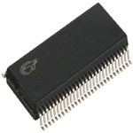
| 供应商器件封装 | 56-SSOP |
| 其它名称 | 428-1627 |
| 包装 | 管件 |
| 可编程输入/输出端数量 | 24 |
| 商标 | Cypress Semiconductor |
| 商标名 | EZ-USB FX2LP |
| 处理器系列 | CY7C68xx |
| 安装类型 | 表面贴装 |
| 安装风格 | SMD/SMT |
| 定时器数量 | 3 Timer |
| 封装 | Tube |
| 封装/外壳 | 56-BSSOP(0.295",7.50mm 宽) |
| 封装/箱体 | SSOP-56 |
| 工作温度 | 0°C ~ 70°C |
| 工作电源电压 | 3.3 V |
| 工厂包装数量 | 26 |
| 应用 | USB 微控制器 |
| 接口 | I²C, USB, USART |
| 接口类型 | GPIF, I2C, USART |
| 控制器系列 | CY7C680xx |
| 数据RAM大小 | 16 kB |
| 数据Ram类型 | SRAM |
| 数据总线宽度 | 8 bit/16 bit |
| 最大工作温度 | + 70 C |
| 最大时钟频率 | 48 MHz |
| 最小工作温度 | 0 C |
| 标准包装 | 390 |
| 核心 | 8051 |
| 核心处理器 | 8051 |
| 片上ADC | No |
| 特色产品 | http://www.digikey.com/cn/zh/ph/Cypress/USBmicrocontrollers.html |
| 电压-电源 | 3 V ~ 3.6 V |
| 电源电压-最大 | 3.6 V |
| 电源电压-最小 | 3 V |
| 程序存储器类型 | ROMless |
| 系列 | CY7C68013A |
| 输入/输出端数量 | 24 I/O |


- 商务部:美国ITC正式对集成电路等产品启动337调查
- 曝三星4nm工艺存在良率问题 高通将骁龙8 Gen1或转产台积电
- 太阳诱电将投资9.5亿元在常州建新厂生产MLCC 预计2023年完工
- 英特尔发布欧洲新工厂建设计划 深化IDM 2.0 战略
- 台积电先进制程称霸业界 有大客户加持明年业绩稳了
- 达到5530亿美元!SIA预计今年全球半导体销售额将创下新高
- 英特尔拟将自动驾驶子公司Mobileye上市 估值或超500亿美元
- 三星加码芯片和SET,合并消费电子和移动部门,撤换高东真等 CEO
- 三星电子宣布重大人事变动 还合并消费电子和移动部门
- 海关总署:前11个月进口集成电路产品价值2.52万亿元 增长14.8%
PDF Datasheet 数据手册内容提取
Please note that Cypress is an Infineon Technologies Company. The document following this cover page is marked as “Cypress” document as this is the company that originally developed the product. Please note that Infineon will continue to offer the product to new and existing customers as part of the Infineon product portfolio. Continuity of document content The fact that Infineon offers the following product as part of the Infineon product portfolio does not lead to any changes to this document. Future revisions will occur when appropriate, and any changes will be set out on the document history page. Continuity of ordering part numbers Infineon continues to support existing part numbers. Please continue to use the ordering part numbers listed in the datasheet for ordering. www.infineon.com
CY7C68013A/CY7C68014A CY7C68015A/CY7C68016A ® EZ-USB FX2LP™ USB Microcontroller High-Speed USB Peripheral Controller EZ-USB® FX2LP™ USB Microcontroller High-Speed USB Peripheral Controller Features ■3.3-V operation with 5-V tolerant inputs ■Vectored USB interrupts and GPIF/FIFO interrupts ■USB 2.0 USB IF Hi-Speed certified (TID # 40460272) ■Separate data buffers for the setup and data portions of a ■Single-chip integrated USB 2.0 transceiver, smart SIE, and CONTROL transfer enhanced 8051 microprocessor ■Integrated I2C controller; runs at 100 or 400 kHz[1] ■Fit-, form-, and function-compatible with the FX2 ❐Pin-compatible0 ■Four integrated FIFOs ❐Object-code-compatible ❐Integrated glue logic and FIFOs lower system cost ❐Functionally compatible (FX2LP is a superset) ❐Automatic conversion to and from 16-bit buses ❐Master or slave operation ■Ultra-low power: I no more than 85 mA in any mode CC ❐Uses external clock or asynchronous strobes ❐Ideal for bus- and battery-powered applications ❐Easy interface to ASIC and DSP ICs ■Software: 8051 code runs from: ■Available in commercial and industrial temperature grades (all ❐Internal RAM, which is downloaded through USB packages except VFBGA) ❐Internal RAM, which is loaded from EEPROM ❐External memory device (128-pin package) Features (CY7C68013A/14A only) ■16 KB of on-chip code/data RAM ■CY7C68014A: Ideal for battery-powered applications ■Four programmable BULK, INTERRUPT, and ❐Suspend current: 100 A (typ) ISOCHRONOUS endpoints ■CY7C68013A: Ideal for nonbattery-powered applications ❐Buffering options: Double, triple, and quad ❐Suspend current: 300 A (typ) ■Additional programmable (BULK/INTERRUPT) 64-byte ■Available in five Pb-free packages with up to 40 GPIOs endpoint ❐128-pin TQFP (40 GPIOs), 100-pin TQFP (40 GPIOs), 56-pin ■8-bit or 16-bit external data interface QFN (24 GPIOs), 56-pin SSOP (24 GPIOs), and 56-pin VFBGA (24 GPIOs) ■Smart media standard ECC generation Features (CY7C68015A/16A only) ■GPIF™ (general programmable interface) ❐Enables direct connection to most parallel interfaces ■CY7C68016A: Ideal for battery-powered applications ❐Programmable waveform descriptors and configuration ❐Suspend current: 100 A (typ) registers to define waveforms ■CY7C68015A: Ideal for nonbattery-powered applications ❐Supports multiple ready (RDY) inputs and control (CTL) ❐Suspend current: 300 A (typ) outputs ■Available in Pb-free 56-pin QFN package (26 GPIOs) ■Integrated, industry-standard, enhanced 8051 ❐48-MHz, 24-MHz, or 12-MHz CPU operation ■Two more GPIOs than CY7C68013A/14A enabling additional ❐Four clocks per instruction cycle features in the same footprint ❐Two USARTs Functional Description ❐Three counter/timers ❐Expanded interrupt system For a complete list of related resources, click here. ❐Two data pointers Errata: For information on silicon errata, see “Errata” on page68. Details include trigger conditions, devices affected, and proposed workaround. Note 1. The actual I2C clock frequency will be different. The measured I2C clock frequency when set for 100 kHz and 400 kHz is around 85 kHz and 300 kHz respectively. CypressSemiconductorCorporation • 198 Champion Court • SanJose, CA 95134-1709 • 408-943-2600 Document Number: 38-08032 Rev. AC Revised July 26, 2019
CY7C68013A/CY7C68014A CY7C68015A/CY7C68016A More Information Cypress provides a wealth of data at www.cypress.com to help you to select the right device for your design, and to help you to quickly and effectively integrate the device into your design. For a comprehensive list of resources, see the application note AN65209 - Getting Started with FX2LP. ■Overview: USB Portfolio, USB Roadmap EZ-USB FX2LP Development Kit ■USB 2.0 Product Selectors: FX2LP, AT2LP, NX2LP-Flex, SX2 The CY3684 EZ-USB FX2LP Development Kit is a complete development resource for FX2LP. It provides a platform to ■Application notes: Cypress offers a large number of USB appli- develop and test custom projects using FX2LP. The cation notes covering a broad range of topics, from basic to development kit contains collateral materials for the firmware, advanced level. Recommended application notes for getting hardware, and software aspects of a design using FX2LP. started with FX2LP are: ❐AN65209 - Getting Started with FX2LP GPIF™ Designer ❐AN15456 - Guide to Successful EZ-USB® FX2LP™ and FX2LP™ General Programmable Interface (GPIF) provides an EZ-USB FX1™ Hardware Design and Debug independent hardware unit, which creates the data and control ❐AN50963 - EZ-USB® FX1™/FX2LP™ Boot Options signals required by an external interface. FX2LP GPIF Designer ❐AN66806 - EZ-USB® FX2LP™ GPIF Design Guide allows users to create and modify GPIF waveform descriptors for ❐AN61345 - Implementing an FX2LP™- FPGA Interface EZ-USB FX2/ FX2LP family of chips using a graphical user ❐AN57322 - Interfacing SRAM with FX2LP over GPIF interface. Extensive discussion of general GPIF discussion and programming using GPIF Designer is included in FX2LP ❐AN4053 - Streaming Data through Isochronous/Bulk End- points on EZ-USB® FX2 and EZUSB FX2LP Technical Reference Manual and GPIF Designer User Guide, ❐AN63787 - EZ-USB® FX2LP™ GPIF and Slave FIFO Con- distributed with GPIF Designer. AN66806 - Getting Started with figuration Examples using 8-bit Asynchronous Interface EZ-USB® FX2LP™ GPIF can be a good starting point. For complete list of Application notes, click here. ■Code Examples: ❐USB Hi-Speed ■Technical Reference Manual (TRM): ❐EZ-USB FX2LP Technical Reference Manual ■Reference Designs: ❐CY4661 - External USB Hard Disk Drives (HDD) with Finger- print Authentication Security ❐FX2LP DMB-T/H TV Dongle reference design ■Models: IBIS Document Number: 38-08032 Rev. AC Page 2 of 75
CY7C68013A/CY7C68014A CY7C68015A/CY7C68016A Logic Block Diagram High-performance micro 24 MHz using standard tools Ext. XTAL with lower-power options FX2LP 16) 8) dress ( Data ( d A /0.5 I2C VCC x20 /1.0 8051 Core Master PLL /2.0 fo1u2r /c2l4o/c4k8s /McyHczle, us (8) Additional I/Os (24) Abundant I/O 1.5k B including two USARTs cfuolln snpeecetedd for Data 6) / ADDR (9) pGroegnrearmalmable I/F DD+– XU2CS.V0BR SUCmSYaBrt 1R6A KMB Address (1 ECC GPIF CRTDLY ((66)) sAtotTa AAnPdSaII,Cr dE/sDP SsPu,P ce hotc ra .bsus Integrated 1.1/2.0 full speed and Engine high speed 4 kB Up to 96 MBytes/s XCVR FIFO 8/16 burst rate Enhanced USB core “Soft Configuration” FIFO and endpoint memory Simplifies 8051 code Easy firmware changes (master or slave operation) Cypress’s EZ-USB® FX2LP™ (CY7C68013A/14A) is a With EZ-USB FX2LP, the Cypress Smart SIE handles most of low-power version of the EZ-USB FX2™(CY7C68013), which is the USB 1.1 and 2.0 protocol in hardware, freeing the embedded a highly integrated, low-power USB 2.0 microcontroller. By microcontroller for application-specific functions and decreasing integrating the USB 2.0 transceiver, serial interface engine (SIE), the development time to ensure USB compatibility. enhanced 8051 microcontroller, and a programmable peripheral The general programmable interface (GPIF) and Master/Slave interface in a single chip, Cypress has created a cost-effective Endpoint FIFO (8-bit or 16-bit data bus) provide an easy and solution that provides superior time-to-market advantages with glueless interface to popular interfaces such as ATA, UTOPIA, low power to enable bus-powered applications. EPP, PCMCIA, and most DSP/processors. The ingenious architecture of FX2LP results in data transfer The FX2LP draws less current than the FX2 (CY7C68013), has rates of over 53 Mbytes per second (the maximum allowable double the on-chip code/data RAM, and is fit, form, and function USB 2.0 bandwidth), while still using a low-cost 8051 compatible with the 56-, 100-, and 128-pin FX2. microcontroller in a package as small as a 56 VFBGA (5mm × 5mm). Because it incorporates the USB 2.0 transceiver, the Five packages are defined for the family: 56-ball VFBGA, 56-pin FX2LP is more economical, providing a smaller-footprint solution SSOP, 56-pin QFN, 100-pin TQFP, and 128-pin TQFP. than a USB 2.0 SIE or external transceiver implementations. Document Number: 38-08032 Rev. AC Page 3 of 75
CY7C68013A/CY7C68014A CY7C68015A/CY7C68016A Contents Applications ......................................................................5 Data Memory Write ...................................................45 Functional Overview ........................................................5 PORTC Strobe Feature Timings ...............................46 USB Signaling Speed ..................................................5 GPIF Synchronous Signals .......................................47 8051 Microprocessor ...................................................5 Slave FIFO Synchronous Read .................................48 I2C Bus ........................................................................5 Slave FIFO Asynchronous Read ...............................49 Buses ..........................................................................5 Slave FIFO Synchronous Write .................................50 USB Boot Methods ......................................................6 Slave FIFO Asynchronous Write ...............................51 ReNumeration .............................................................6 Slave FIFO Synchronous Packet End Strobe ...........52 Bus-Powered Applications ..........................................6 Slave FIFO Asynchronous Packet End Strobe .........54 Interrupt System ..........................................................6 Slave FIFO Output Enable ........................................54 Reset and Wakeup ......................................................9 Slave FIFO Address to Flags/Data ............................54 Program/Data RAM ...................................................10 Slave FIFO Synchronous Address ............................55 Register Addresses ...................................................12 Slave FIFO Asynchronous Address ..........................55 Endpoint RAM ...........................................................13 Sequence Diagram ....................................................56 External FIFO Interface .............................................15 Ordering Information ......................................................60 GPIF ..........................................................................15 Ordering Code Definitions .........................................60 ECC Generation ........................................................16 Package Diagrams ..........................................................61 USB Uploads and Downloads ...................................16 PCB Layout Recommendations ....................................65 Autopointer Access ...................................................16 Quad Flat Package No Leads (QFN) Package I2C Controller .............................................................16 Design Notes ...................................................................66 Compatible Acronyms ........................................................................67 with Previous Generation EZ-USB FX2 ............................17 Document Conventions .................................................67 CY7C68013A/14A Units of Measure .......................................................67 and CY7C68015A/16A Differences ..................................17 Errata ...............................................................................68 Pin Assignments ............................................................18 Part Numbers Affected ..............................................68 CY7C68013A/15A Pin Descriptions ..........................25 CY7C68013A/14A/15A/16A Qualification Status ......68 Register Summary ..........................................................34 CY7C68013A/14A/15A/16A Errata Summary ...........68 Absolute Maximum Ratings ..........................................41 Document History Page .................................................69 Operating Conditions .....................................................41 Sales, Solutions, and Legal Information ......................75 Thermal Characteristics .................................................41 Worldwide Sales and Design Support .......................75 DC Electrical Characteristics ........................................42 Products ....................................................................75 USB Transceiver .......................................................42 PSoC® Solutions ......................................................75 AC Electrical Characteristics ........................................43 Cypress Developer Community .................................75 USB Transceiver .......................................................43 Technical Support .....................................................75 Program Memory Read .............................................43 Data Memory Read ...................................................44 Document Number: 38-08032 Rev. AC Page 4 of 75
CY7C68013A/CY7C68014A CY7C68015A/CY7C68016A Applications Figure 1. Crystal Configuration ■Portable video recorder C1 24 MHz C2 ■MPEG/TV conversion ■DSL modems 12 pF 12 pF ■ATA interface ■Memory card readers 20 × PLL ■Legacy conversion devices ■Cameras 12-pF capacitor values assume a trace capacitance of 3 pF per side on a four-layer FR4 PCA ■Scanners The CLKOUT pin, which can be three-stated and inverted using ■Wireless LAN internal control bits, outputs the 50% duty cycle 8051 clock, at ■MP3 players the selected 8051 clock frequency: 48 MHz, 24 MHz, or 12 MHz. ■Networking USARTs The “Reference Designs” section of the Cypress web site FX2LP contains two standard 8051 USARTs, addressed through provides additional tools for typical USB 2.0 applications. Each Special Function Register (SFR) bits. The USART interface pins reference design comes complete with firmware source and are available on separate I/O pins, and are not multiplexed with object code, schematics, and documentation. Visit port pins. www.cypress.com for more information. UART0 and UART1 can operate using an internal clock at Functional Overview 230KBaud with no more than 1% baud rate error. 230 KBaud operation is achieved by an internally derived clock source that generates overflow pulses at the appropriate time. The internal USB Signaling Speed clock adjusts for the 8051 clock rate (48 MHz, 24 MHz, and FX2LP operates at two of the three rates defined in the USB 12MHz) such that it always presents the correct frequency for Specification Revision 2.0, dated April 27, 2000: the 230-KBaud operation[2]. ■Full speed, with a signaling bit rate of 12 Mbps Special Function Registers ■High speed, with a signaling bit rate of 480 Mbps Certain 8051 SFR addresses are populated to provide fast FX2LP does not support the Low Speed signaling mode of access to critical FX2LP functions. These SFR additions are 1.5Mbps. shown in Table 1 on page 6. Bold type indicates nonstandard, enhanced 8051 registers. The two SFR rows that end with “0” 8051 Microprocessor and “8” contain bit-addressable registers. The four I/O ports A to D use the SFR addresses used in the standard 8051 for ports 0 The 8051 microprocessor embedded in the FX2LP family has to 3, which are not implemented in FX2LP. Because of the faster 256 bytes of register RAM, an expanded interrupt system, three and more efficient SFR addressing, the FX2LP I/O ports are not timer/counters, and two USARTs. addressable in external RAM space (using the MOVX instruction). 8051 Clock Frequency FX2LP has an on-chip oscillator circuit that uses an external I2C Bus 24-MHz (±100 ppm) crystal with the following characteristics: FX2LP supports the I2C bus as a master only at 100/400 kHz[3]. ■Parallel resonant SCL and SDA pins have open-drain outputs and hysteresis inputs. These signals must be pulled up to 3.3V, even if no I2C ■Fundamental mode device is connected. ■500-W drive level Buses ■12-pF (5% tolerance) load capacitors All packages, 8-bit or 16-bit “FIFO” bidirectional data bus, An on-chip PLL multiplies the 24-MHz oscillator up to 480 MHz, multiplexed on I/O ports B and D. 128-pin package: adds 16-bit as required by the transceiver/PHY; internal counters divide it output-only 8051 address bus, 8-bit bidirectional data bus. down for use as the 8051 clock. The default 8051 clock frequency is 12 MHz. The clock frequency of the 8051 can be changed by the 8051 through the CPUCS register, dynamically. Notes 2. 115-KBaud operation is also possible by programming the 8051 SMOD0 or SMOD1 bits to a “1” for UART0, UART1, or both respectively. 3. The actual I2C clock frequency will be different.The measured I2C clock frequency when set for 100 kHz and 400 kHz is around 85 kHz and 300 kHz respectively. Document Number: 38-08032 Rev. AC Page 5 of 75
CY7C68013A/CY7C68014A CY7C68015A/CY7C68016A Table 1. Special Function Registers x 8x 9x Ax Bx Cx Dx Ex Fx 0 IOA IOB IOC IOD SCON1 PSW ACC B 1 SP EXIF INT2CLR IOE SBUF1 – – – 2 DPL0 MPAGE INT4CLR OEA – – – – 3 DPH0 – – OEB – – – – 4 DPL1 – – OEC – – – – 5 DPH1 – – OED – – – – 6 DPS – – OEE – – – – 7 PCON – – – – – – – 8 TCON SCON0 IE IP T2CON EICON EIE EIP 9 TMOD SBUF0 – – – – – – A TL0 AUTOPTRH1 EP2468STAT EP01STAT RCAP2L – – – B TL1 AUTOPTRL1 EP24FIFOFLGS GPIFTRIG RCAP2H – – – C TH0 reserved EP68FIFOFLGS TL2 – – – D TH1 AUTOPTRH2 – GPIFSGLDATH TH2 – – – E CKCON AUTOPTRL2 – GPIFSGLDATLX – – – – F – reserved AUTOPTRSET-UP GPIFSGLDATLNOX – – – – USB Boot Methods Two control bits in the USBCS (USB Control and Status) register During the power-up sequence, internal logic checks the I2C port control the ReNumeration process: DISCON and RENUM. To simulate a USB disconnect, the firmware sets DISCON to 1. To for the connection of an EEPROM whose first byte is either 0xC0 reconnect, the firmware clears DISCON to 0. or 0xC2. If found, it uses the VID/PID/DID values in the EEPROM in place of the internally stored values (0xC0), or it boot-loads the Before reconnecting, the firmware sets or clears the RENUM bit EEPROM contents into internal RAM (0xC2). If no EEPROM is to indicate whether the firmware or the Default USB Device detected, FX2LP enumerates using internally stored descriptors. handles device requests over endpoint zero: if RENUM = 0, the The default ID values for FX2LP are VID/PID/DID (0x04B4, Default USB Device handles device requests; if RENUM = 1, the 0x8613, 0xAxxx where xxx = Chip revision)[4]. firmware services the requests. Table 2. Default ID Values for FX2LP Bus-Powered Applications Default VID/PID/DID The FX2LP fully supports bus-powered designs by enumerating with less than 100 mA as required by the USB 2.0 specification. Vendor ID 0x04B4 Cypress Semiconductor Product ID 0x8613 EZ-USB FX2LP Interrupt System Depends on chip revision INT2 Interrupt Request and Enable Registers Device release 0xAnnn (nnn = chip revision where first silicon = 001) FX2LP implements an autovector feature for INT2 and INT4. There are 27 INT2 (USB) vectors, and 14 INT4 (FIFO/GPIF) vectors. See EZ-USB Technical Reference Manual (TRM) for ReNumeration more details. Because the FX2LP’s configuration is soft, one chip can take on USB Interrupt Autovectors the identities of multiple distinct USB devices. The main USB interrupt is shared by 27 interrupt sources. To When first plugged into USB, the FX2LP enumerates save the code and processing time that is required to identify the automatically and downloads firmware and USB descriptor individual USB interrupt source, the FX2LP provides a second tables over the USB cable. Next, the FX2LP enumerates again, level of interrupt vectoring, called Autovectoring. When a USB this time as a device defined by the downloaded information. interrupt is asserted, the FX2LP pushes the program counter to This patented two step process called ReNumeration™ happens its stack, and then jumps to the address 0x0043 where it expects instantly when the device is plugged in, without a hint that the to find a “jump” instruction to the USB interrupt service routine. initial download step has occurred. Note 4. The I2C bus SCL and SDA pins must be pulled up, even if an EEPROM is not connected. Otherwise this detection method does not work properly. Document Number: 38-08032 Rev. AC Page 6 of 75
CY7C68013A/CY7C68014A CY7C68015A/CY7C68016A The FX2LP jump instruction is encoded as follows: Table 3. INT2 USB Interrupts USB INTERRUPT TABLE FOR INT2 Priority INT2VEC Value Source Notes 1 00 SUDAV Setup data available 2 04 SOF Start of frame (or microframe) 3 08 SUTOK Setup token received 4 0C SUSPEND USB suspend request 5 10 USB RESET Bus reset 6 14 HISPEED Entered high speed operation 7 18 EP0ACK FX2LP ACK’d the CONTROL Handshake 8 1C reserved 9 20 EP0-IN EP0-IN ready to be loaded with data 10 24 EP0-OUT EP0-OUT has USB data 11 28 EP1-IN EP1-IN ready to be loaded with data 12 2C EP1-OUT EP1-OUT has USB data 13 30 EP2 IN: buffer available. OUT: buffer has data 14 34 EP4 IN: buffer available. OUT: buffer has data 15 38 EP6 IN: buffer available. OUT: buffer has data 16 3C EP8 IN: buffer available. OUT: buffer has data 17 40 IBN IN-Bulk-NAK (any IN endpoint) 18 44 reserved 19 48 EP0PING EP0 OUT was pinged and it NAK’d 20 4C EP1PING EP1 OUT was pinged and it NAK’d 21 50 EP2PING EP2 OUT was pinged and it NAK’d 22 54 EP4PING EP4 OUT was pinged and it NAK’d 23 58 EP6PING EP6 OUT was pinged and it NAK’d 24 5C EP8PING EP8 OUT was pinged and it NAK’d 25 60 ERRLIMIT Bus errors exceeded the programmed limit 26 64 – – 27 68 – Reserved 28 6C – Reserved 29 70 EP2ISOERR ISO EP2 OUT PID sequence error 30 74 EP4ISOERR ISO EP4 OUT PID sequence error 31 78 EP6ISOERR ISO EP6 OUT PID sequence error 32 7C EP8ISOERR ISO EP8 OUT PID sequence error If Autovectoring is enabled (AV2EN = 1 in the INTSET-UP register), the FX2LP substitutes its INT2VEC byte. Therefore, if the high byte (“page”) of a jump table address is preloaded at the location 0x0044, the automatically inserted INT2VEC byte at 0x0045 directs the jump to the correct address out of the 27 addresses within the page. Document Number: 38-08032 Rev. AC Page 7 of 75
CY7C68013A/CY7C68014A CY7C68015A/CY7C68016A FIFO/GPIF Interrupt (INT4) Just as the USB Interrupt is shared among 27 individual USB interrupt sources, the FIFO/GPIF interrupt is shared among 14 individual FIFO/GPIF sources. The FIFO/GPIF Interrupt, similar to the USB Interrupt, can employ autovectoring. Table4 shows the priority and INT4VEC values for the 14 FIFO/GPIF interrupt sources. Table 4. Individual FIFO/GPIF Interrupt Sources Priority INT4VEC Value Source Notes 1 80 EP2PF Endpoint 2 programmable flag 2 84 EP4PF Endpoint 4 programmable flag 3 88 EP6PF Endpoint 6 programmable flag 4 8C EP8PF Endpoint 8 programmable flag 5 90 EP2EF Endpoint 2 empty flag [5] 6 94 EP4EF Endpoint 4 empty flag 7 98 EP6EF Endpoint 6 empty flag 8 9C EP8EF Endpoint 8 empty flag 9 A0 EP2FF Endpoint 2 full flag 10 A4 EP4FF Endpoint 4 full flag 11 A8 EP6FF Endpoint 6 full flag 12 AC EP8FF Endpoint 8 full flag 13 B0 GPIFDONE GPIF operation complete 14 B4 GPIFWF GPIF waveform If Autovectoring is enabled (AV4EN = 1 in the INTSET-UP register), the FX 2LP substitutes its INT4VEC byte. Therefore, if the high byte (“page”) of a jump-table address is preloaded at location 0x0054, the automatically inserted INT4VEC byte at 0x0055 directs the jump to the correct address out of the 14 addresses within the page. When the ISR occurs, the FX2LP pushes the program counter to its stack then jumps to address 0x0053, where it expects to find a “jump” instruction to the interrupt service routine (ISR). Note 5. Errata: In Slave FIFO Asynchronous Word Wide mode, if a single word data is transferred from the USB host to EP2, configured as OUT Endpoint (EP) in the first transaction, then the Empty flag behaves incorrectly. This does not happen if the data size is more than one word in the first transaction. For more information, see the “Errata” on page68. Document Number: 38-08032 Rev. AC Page 8 of 75
CY7C68013A/CY7C68014A CY7C68015A/CY7C68016A Reset and Wakeup Figure2 shows a power-on reset condition and a reset applied during operation. A power-on reset is defined as the time reset Reset Pin that is asserted while power is being applied to the circuit. A The input pin, RESET#, resets the FX2LP when asserted. This powered reset is when the FX2LP is powered on and operating pin has hysteresis and is active LOW. When a crystal is used with and the RESET# pin is asserted. the CY7C680xxA, the reset period must enable stabilization of Cypress provides an application note which describes and the crystal and the PLL. This reset period must be approximately recommends power-on reset implementation. For more 5ms after VCC reaches 3.0V. If the crystal input pin is driven by information about reset implementation for the FX2 family of a clock signal, the internal PLL stabilizes in 200s after VCC has products, visit http://www.cypress.com. reached 3.0V[6]. Figure 2. Reset Timing Plots RESET# RESET# VIL VIL 3.3V 3.3V 3.0V VCC VCC 0V 0V T T RESET RESET Power on Reset Powered Reset Wakeup Pins Table 5. Reset Timing Values The 8051 puts itself and the rest of the chip into a power-down Condition T mode by setting PCON.0 = 1. This stops the oscillator and PLL. RESET When WAKEUP is asserted by external logic, the oscillator Power-on reset with crystal 5 ms restarts after the PLL stabilizes, and the 8051 receives a wakeup Power-on reset with external interrupt. This applies irrespective of whether FX2LP is 200 s + clock stability time clock connected to the USB. Powered reset 200 s The FX2LP exits the power-down (USB suspend) state by using one of the following methods: ■USB bus activity (if D+/D– lines are left floating, noise on these lines may indicate activity to the FX2LP and initiate a wakeup) ■External logic asserts the WAKEUP pin ■External logic asserts the PA3/WU2 pin The second wakeup pin, WU2, can also be configured as a general-purpose I/O pin. This enables a simple external R-C network to be used as a periodic wakeup source. WAKEUP is by default active LOW. Document Number: 38-08032 Rev. AC Page 9 of 75
CY7C68013A/CY7C68014A CY7C68015A/CY7C68016A Program/Data RAM suppressed for memory spaces that exist inside the chip. This enables the user to connect a 64 KB memory without requiring Size address decodes to keep clear of internal memory spaces. The FX2LP has 16 KB of internal program/data RAM, where Only the internal 16 KB and scratch pad 0.5 KB RAM spaces PSEN#/RD# signals are internally ORed to enable the 8051 to have the following access: access it as both program and data memory. No USB control registers appears in this space. ■USB download Two memory maps are shown in the following diagrams: ■USB upload Figure3 shows the Internal Code Memory, EA = 0. ■Setup data pointer Figure 4 on page 11 shows the External Code Memory, EA = 1. ■I2C interface boot load Internal Code Memory, EA = 0 External Code Memory, EA = 1 This mode implements the internal 16 KB block of RAM (starting The bottom 16 KB of program memory is external and therefore at 0) as combined code and data memory. When external RAM the bottom 16 KB of internal RAM is accessible only as a data or ROM is added, the external read and write strobes are memory. Figure 3. Internal Code Memory, EA = 0 Inside FX2LP Outside FX2LP FFFF 7.5 KB USB regs and (OK to populate 4K FIFO buffers data memory (RD#,WR#) here—RD#/WR# E200 strobes are not E1FF active) 0.5 KB RAM E000 Data (RD#,WR#)* 48 KB External 40 KB Code External Memory Data (PSEN#) Memory (RD#,WR#) 3FFF (Ok to populate (OK to populate 16 KB RAM data memory program Code and Data here—RD#/WR# memory here— (PSEN#,RD#,WR#)* strobes are not PSEN# strobe active) is not active) 0000 Data Code *SUDPTR, USB upload/download, I2C interface boot access Note 6. If the external clock is powered at the same time as the CY7C680xxA and has a stabilization wait period, it must be added to the 200 s. Document Number: 38-08032 Rev. AC Page 10 of 75
CY7C68013A/CY7C68014A CY7C68015A/CY7C68016A Figure 4. External Code Memory, EA = 1 Inside FX2LP Outside FX2LP FFFF 7.5 KB USB regs and (OK to populate 4K FIFO buffers data memory (RD#,WR#) here—RD#/WR# E200 strobes are not E1FF 0.5 KB RAM active) E000 Data (RD#,WR#)* 40 KB External Data 64 KB Memory External (RD#,WR#) Code Memory (PSEN#) 3FFF 16 KB (Ok to populate data memory RAM here—RD#/WR# Data strobes are not (RD#,WR#)* active) 0000 Data Code *SUDPTR, USB upload/download, I2C interface boot access Document Number: 38-08032 Rev. AC Page 11 of 75
CY7C68013A/CY7C68014A CY7C68015A/CY7C68016A Register Addresses FFFF 4 KB EP2-EP8 buffers (8 x 512) F000 EFFF 2 KB RESERVED E800 E7FF 64 BEP1IN E7C0 E7BF 64 Bytes EP1OUT E780 E77F 64 Bytes EP0 IN/OUT E740 E73F 64 Bytes RESERVED E700 E6FF 8051 Addressable Registers (512) E500 E4FF Reserved (128) E480 E47F 128 Bytes GPIF Waveforms E400 E3FF Reserved (512) E200 E1FF 512 Bytes 8051 xdata RAM E000 Document Number: 38-08032 Rev. AC Page 12 of 75
CY7C68013A/CY7C68014A CY7C68015A/CY7C68016A Endpoint RAM Setup Data Buffer A separate 8-byte buffer at 0xE6B8-0xE6BF holds the setup data Size from a CONTROL transfer. ■3 × 64 bytes (Endpoints 0 and 1) Endpoint Configurations (Hi-Speed Mode) ■8 × 512 bytes (Endpoints 2, 4, 6, 8) Endpoints 0 and 1 are the same for every configuration. Endpoint 0 is the only CONTROL endpoint, and endpoint 1 can Organization be either BULK or INTERRUPT. ■EP0 The endpoint buffers can be configured in any 1 of the 12 ■Bidirectional endpoint zero, 64-byte buffer configurations shown in the vertical columns. When operating in the Full-Speed BULK mode, only the first 64 bytes of each buffer ■EP1IN, EP1OUT are used. For example, in Hi-Speed mode, the max packet size is 512 bytes, but in Full-Speed mode, it is 64 bytes. Even though ■64 byte buffers, bulk or interrupt a buffer is configured to a 512-byte buffer, in Full-Speed mode, ■EP2, 4, 6, 8 only the first 64 bytes are used. The unused endpoint buffer space is not available for other operations. An example endpoint ■Eight 512-byte buffers, bulk, interrupt, or isochronous. EP4 and configuration is the EP2–1024 double-buffered; EP6–512 EP8 can be double buffered; EP2 and 6 can be either double, quad-buffered (column8). triple, or quad buffered. For Hi-Speed endpoint configuration options, see Figure5. Figure 5. Endpoint Configuration EP0 IN&OUT 64 64 64 64 64 64 64 64 64 64 64 64 EP1 IN 64 64 64 64 64 64 64 64 64 64 64 64 EP1 OUT 64 64 64 64 64 64 64 64 64 64 64 64 EP2 EP2 EP2 EP2 EP2 EP2 EP2 EP2 EP2 EP2 EP2 EP2 512 512 512 512 512 512 512 1024 1024 1024 512 512 512 512 512 512 512 1024 1024 EP4 EP4 EP4 512 512 512 512 512 512 512 1024 1024 1024 EP6 1024 1024 512 512 512 512 512 512 512 EP6 EP6 EP6 EP6 EP6 EP6 EP6 EP6 EP6 512 1024 512 512 512 512 512 512 1024 1024 1024 1024 1024 512 512 512 512 512 512 512 EP8 EP8 EP8 EP8 EP8 512 512 1024 512 512 1024 512 512 1024 512 512 1024 512 512 512 512 512 512 512 512 1 2 3 4 5 6 7 8 9 10 11 12 Document Number: 38-08032 Rev. AC Page 13 of 75
CY7C68013A/CY7C68014A CY7C68015A/CY7C68016A Default Full-Speed Alternate Settings Table 6. Default Full Speed Alternate Settings[7, 8] Alternate Setting 0 1 2 3 ep0 64 64 64 64 ep1out 0 64 bulk 64 int 64 int ep1in 0 64 bulk 64 int 64 int ep2 0 64 bulk out (2×) 64 int out (2×) 64 iso out (2×) ep4 0 64 bulk out (2×) 64 bulk out (2×) 64 bulk out (2×) ep6 0 64 bulk in (2×) 64 int in (2×) 64 iso in (2×) ep8 0 64 bulk in (2×) 64 bulk in (2×) 64 bulk in (2×) Default High Speed Alternate Settings Table 7. Default Hi-Speed Alternate Settings[7, 8] Alternate Setting 0 1 2 3 ep0 64 64 64 64 ep1out 0 512 bulk[9] 64 int 64 int ep1in 0 512 bulk[9] 64 int 64 int ep2 0 512 bulk out (2×) 512 int out (2×) 512 iso out (2×) ep4 0 512 bulk out (2×) 512 bulk out (2×) 512 bulk out (2×) ep6 0 512 bulk in (2×) 512 int in (2×) 512 iso in (2×) ep8 0 512 bulk in (2×) 512 bulk in (2×) 512 bulk in (2×) Notes 7. “0” means “not implemented.” 8. “2×” means “double buffered.” 9. Even though these buffers are 64 bytes, they are reported as 512 for USB 2.0 compliance. The user must never transfer packets larger than 64 bytes to EP1. Document Number: 38-08032 Rev. AC Page 14 of 75
CY7C68013A/CY7C68014A CY7C68015A/CY7C68016A External FIFO Interface Alternatively, an externally supplied clock of 5 MHz–48 MHz feeding the IFCLK pin can be used as the interface clock. IFCLK Architecture can be configured to function as an output clock when the GPIF and FIFOs are internally clocked. An output enable bit in the The FX2LP slave FIFO architecture has eight 512-byte blocks in IFCONFIG register turns this clock output off, if desired. Another the endpoint RAM that directly serve as FIFO memories and are bit within the IFCONFIG register inverts the IFCLK signal controlled by FIFO control signals (such as IFCLK, SLCS#, whether internally or externally sourced. SLRD, SLWR, SLOE, PKTEND, and flags). In operation, some of the eight RAM blocks fill or empty from the GPIF SIE, while the others are connected to the I/O transfer logic. The The GPIF is a flexible 8-bit or 16-bit parallel interface driven by transfer logic takes two forms: the GPIF for internally generated a user-programmable finite state machine. It enables the control signals and the slave FIFO interface for externally CY7C68013A/15A to perform local bus mastering and can controlled transfers. implement a wide variety of protocols such as ATA interface, Master/Slave Control Signals printer parallel port, and Utopia. The FX2LP endpoint FIFOs are implemented as eight physically The GPIF has six programmable control outputs (CTL), nine distinct 25616 RAM blocks. The 8051/SIE can switch any of the address outputs (GPIFADRx), and six general-purpose ready RAM blocks between two domains, the USB (SIE) domain and inputs (RDY). The data bus width can be 8 or 16 bits. Each GPIF the 8051-I/O Unit domain. This switching is done virtually vector defines the state of the control outputs, and determines instantaneously, giving essentially zero transfer time between what state a ready input (or multiple inputs) must be before “USB FIFOs” and “Slave FIFOs.” Because they are physically proceeding. The GPIF vector can be programmed to advance a the same memory, no bytes are actually transferred between FIFO to the next data value, advance an address, etc. A buffers. sequence of the GPIF vectors make up a single waveform that is executed to perform the desired data move between the At any time, some RAM blocks are filling/emptying with the USB FX2LP and the external device. data under SIE control, while other RAM blocks are available to the 8051, the I/O control unit, or both. The RAM blocks operates Six Control OUT Signals as single-port in the USB domain, and dual-port in the 8051-I/O The 100-pin and 128-pin packages bring out all six Control domain. The blocks can be configured as single-, double-, triple-, Output pins (CTL0-CTL5). The 8051 programs the GPIF unit to or quad-buffered as previously shown. define the CTL waveforms. The 56-pin package brings out three The I/O control unit implements either an internal master (M for of these signals, CTL0–CTL2. CTLx waveform edges can be Master) or external master (S for Slave) interface. programmed to make transitions as fast as once per clock In Master (M) mode, the GPIF internally controls FIFOADR[1..0] (20.8ns using a 48-MHz clock). to select a FIFO. The RDY pins (two in the 56-pin package, six Six Ready IN Signals in the 100-pin and 128-pin packages) can be used as flag inputs from an external FIFO or other logic if desired. The GPIF can be The 100-pin and 128-pin packages bring out all six Ready inputs run from either an internally derived clock or externally supplied (RDY0–RDY5). The 8051 programs the GPIF unit to test the clock (IFCLK), at a rate that transfers data up to 96 MBytes/s RDY pins for GPIF branching. The 56-pin package brings out two (48Hz IFCLK with 16-bit interface). of these signals, RDY0–1. In the Slave (S) mode, FX2LP accepts either an internally Nine GPIF Address OUT Signals derived clock or externally supplied clock (IFCLK, max frequency 48 MHz) and SLCS#, SLRD, SLWR, SLOE, PKTEND signals Nine GPIF address lines are available in the 100-pin and 128-pin from external logic. When using an external IFCLK, the external packages, GPIFADR[8..0]. The GPIF address lines enable clock must be present before switching to the external clock with indexing through up to a 512-byte block of RAM. If more address the IFCLKSRC bit. Each endpoint can individually be selected lines are needed, then I/O port pins are used. for byte or word operation by an internal configuration bit and a Long Transfer Mode Slave FIFO Output Enable signal (SLOE) that enables data of the selected width. External logic must ensure that the output In the master mode, the 8051 appropriately sets GPIF enable signal is inactive when writing data to a slave FIFO. The transaction count registers (GPIFTCB3, GPIFTCB2, GPIFTCB1, slave interface can also operate asynchronously, where the or GPIFTCB0) for unattended transfers of up to 232 transactions. SLRD and SLWR signals act directly as strobes, rather than a The GPIF automatically throttles data flow to prevent under or clock qualifier as in synchronous mode. The signals SLRD, overflow until the full number of requested transactions SLWR, SLOE, and PKTEND are gated by the signal SLCS#. complete. The GPIF decrements the value in these registers to represent the current status of the transaction. GPIF and FIFO Clock Rates An 8051 register bit selects one of two frequencies for the internally supplied interface clock: 30 MHz and 48 MHz. Document Number: 38-08032 Rev. AC Page 15 of 75
CY7C68013A/CY7C68014A CY7C68015A/CY7C68016A ECC Generation under the control of a mode bit (AUTOPTRSET-UP.0). Using the The EZ-USB can calculate ECCs (Error Correcting Codes)[10] on external FX2LP autopointer access (at 0xE67B–0xE67C) enables the autopointer to access all internal and external RAM data that passes across its GPIF or Slave FIFO interfaces. There to the part. are two ECC configurations: Two ECCs, each calculated over 256 bytes (SmartMedia Standard); and one ECC calculated over Also, autopointers can point to any FX2LP register or endpoint 512 bytes. buffer space. When the autopointer access to external memory is enabled, locations 0xE67B and 0xE67C in XDATA and code The ECC can correct any one-bit error or detect any two-bit error. space cannot be used. ECC Implementation I2C Controller The two ECC configurations are selected by the ECCM bit: FX2LP has one I2C port that is driven by two internal controllers, ECCM = 0 the one that automatically operates at boot time to load Two 3-byte ECCs, each calculated over a 256-byte block of data. VID/PID/DID and configuration information, and another that the This configuration conforms to the SmartMedia Standard. 8051 uses when running to control external I2C devices. The I2C port operates in master mode only. Write any value to ECCRESET, then pass data across the GPIF or Slave FIFO interface. The ECC for the first 256 bytes of data I2C Port Pins is calculated and stored in ECC1. The ECC for the next 256 bytes The I2C pins SCL and SDA must have external 2.2-k pull-up is stored in ECC2. After the second ECC is calculated, the values resistors even if no EEPROM is connected to the FX2LP. in the ECCx registers do not change until ECCRESET is written External EEPROM device address pins must be configured again, even if more data is subsequently passed across the properly. See Table8 for configuring the device address pins. interface. ECCM = 1 Table 8. Strap Boot EEPROM Address Lines to These Values One 3-byte ECC calculated over a 512-byte block of data. Bytes Example EEPROM A2 A1 A0 Write any value to ECCRESET then pass data across the GPIF 16 24LC00[12] N/A N/A N/A or Slave FIFO interface. The ECC for the first 512 bytes of data 128 24LC01 0 0 0 is calculated and stored in ECC1; ECC2 is unused. After the ECC is calculated, the values in ECC1 do not change even if 256 24LC02 0 0 0 more data is subsequently passed across the interface, till 4K 24LC32 0 0 1 ECCRESET is written again. 8K 24LC64 0 0 1 USB Uploads and Downloads 16K 24LC128 0 0 1 The core has the ability to directly edit the data contents of the internal 16-KB RAM and of the internal 512-byte scratch pad I2C Interface Boot Load Access RAM via a vendor-specific command. This capability is normally At power-on reset, the I2C interface boot loader loads the used when soft downloading the user code and is available only VID/PID/DID configuration bytes and up to 16 KB of to and from the internal RAM, only when the 8051 is held in reset. program/data. The available RAM spaces are 16 KB from The available RAM spaces are 16 KB from 0x0000–0x3FFF 0x0000–0x3FFF and 512 bytes from 0xE000–0xE1FF. The 8051 (code/data) and 512 bytes from 0xE000–0xE1FF (scratch pad data RAM)[11]. is in reset. I2C interface boot loads only occur after power-on reset. Autopointer Access I2C Interface General-Purpose Access FX2LP provides two identical autopointers. They are similar to The 8051 can control peripherals connected to the I2C bus using the internal 8051 data pointers but with an additional feature: the I2CTL and I2DAT registers. FX2LP provides I2C master they can optionally increment after every memory access. This control only; it is never an I2C slave. capability is available to and from both internal and external RAM. Autopointers are available in external FX2LP registers Notes 10.To use the ECC logic, the GPIF or Slave FIFO interface must be configured for byte-wide operation. 11.After the data is downloaded from the host, a “loader” can execute from internal RAM to transfer downloaded data to external memory. 12.This EEPROM does not have address pins. Document Number: 38-08032 Rev. AC Page 16 of 75
CY7C68013A/CY7C68014A CY7C68015A/CY7C68016A Compatible with Previous Generation EZ-USB FX2 CY7C68013A/14A and CY7C68015A/16A Differences The EZ-USB FX2LP is form-, fit-, and with minor exceptions, CY7C68013A is identical to CY7C68014A in form, fit, and functionally-compatible with its predecessor, the EZ-USB FX2. functionality. CY7C68015A is identical to CY7C68016A in form, This makes for an easy transition for designers wanting to fit, and functionality. CY7C68014A and CY7C68016A have a upgrade their systems from the FX2 to the FX2LP. The pinout lower suspend current than CY7C68013A and CY7C68015A and package selection are identical and a vast majority of respectively and are ideal for power-sensitive battery firmware previously developed for the FX2 functions in the applications. FX2LP. CY7C68015A and CY7C68016A are available in 56-pin QFN For designers migrating from the FX2 to the FX2LP, a change in package only. Two additional GPIO signals are available on the the bill of material and review of the memory allocation (due to CY7C68015A and CY7C68016A to provide more flexibility when increased internal memory) is required. For more information neither IFCLK or CLKOUT are needed in the 56-pin package. about migrating from EZ-USB FX2 to EZ-USB FX2LP, see the USB developers wanting to convert their FX2 56-pin application application note titled Migrating from EZ-USB FX2 to EZ-USB to a bus-powered system directly benefit from these additional FX2LP available in the Cypress web site. signals. The two GPIOs give developers the signals they need for the power-control circuitry of their bus-powered application Table 9. Part Number Conversion Table without pushing them to a high-pincount version of FX2LP. EZ-USB FX2 EZ-USB FX2LP Package The CY7C68015A is only available in the 56-pin QFN package Part Number Part Number Description Table 10. CY7C68013A/14A and CY7C68015A/16A CY7C68013A-56PVXC or 56-pin CY7C68013-56PVC CY7C68014A-56PVXC SSOP Pin Differences 56-pin CY7C68013A/CY7C68014A CY7C68015A/CY7C68016A CY7C68013-56PVCT CY7C68013A-56PVXCT or SSOP – IFCLK PE0 CY7C68014A-56PVXCT Tape and CLKOUT PE1 Reel CY7C68013A-56LFXC or CY7C68013-56LFC 56-pin QFN CY7C68014A-56LFXC CY7C68013A-100AXC or 100-pin CY7C68013-100AC CY7C68014A-100AXC TQFP CY7C68013A-128AXC or 128-pin CY7C68013-128AC CY7C68014A-128AXC TQFP Document Number: 38-08032 Rev. AC Page 17 of 75
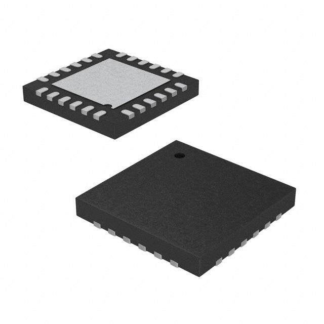
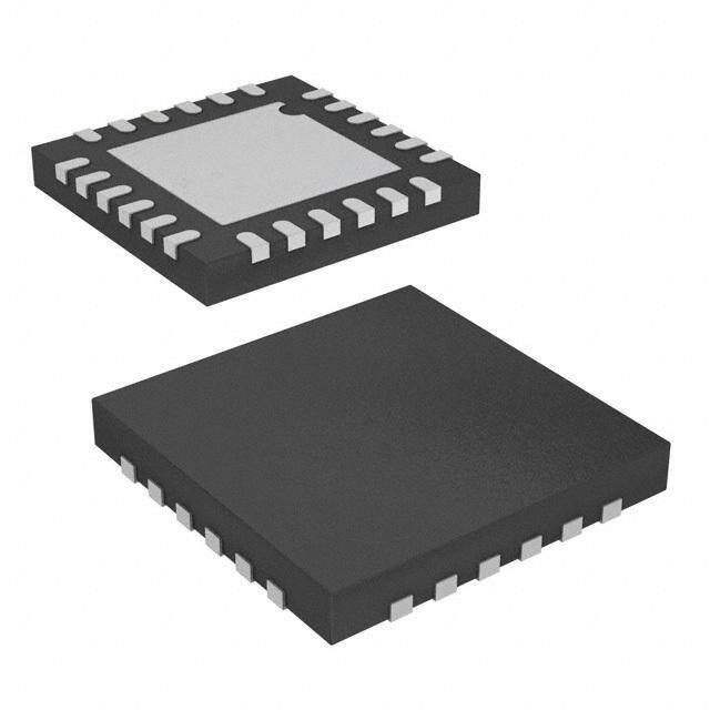
CY7C68013A/CY7C68014A CY7C68015A/CY7C68016A Pin Assignments The 100-pin package adds functionality to the 56-pin package by adding these pins: Figure 6 on page 19 identifies all signals for the five package ■PORTC or alternate GPIFADR[7:0] address signals types. The following pages illustrate the individual pin diagrams, plus a combination diagram showing which of the full set of ■PORTE or alternate GPIFADR[8] address signal and seven signals are available in the 128-pin, 100-pin, and 56-pin additional 8051 signals packages. ■Three GPIF Control signals The signals on the left edge of the 56-pin package in Figure 6 on page 19 are common to all versions in the FX2LP family with ■Four GPIF Ready signals the noted differences between the CY7C68013A/14A and the ■Nine 8051 signals (two USARTs, three timer inputs, INT4, and CY7C68015A/16A. INT5#) Three modes are available in all package versions: Port, GPIF master, and Slave FIFO. These modes define the signals on the ■BKPT, RD#, WR#. right edge of the diagram. The 8051 selects the interface mode The 128-pin package adds the 8051 address and data buses using the IFCONFIG[1:0] register bits. Port mode is the power on plus control signals. Note that two of the required signals, RD# default configuration. and WR#, are present in the 100-pin version. In the 100-pin and 128-pin versions, an 8051 control bit can be set to pulse the RD# and WR# pins when the 8051 reads from/writes to PORTC. This feature is enabled by setting the PORTCSTB bit in the CPUCS register. PORTC Strobe Feature Timings on page 46 displays the timing diagram of the read and write strobing function on accessing PORTC. Document Number: 38-08032 Rev. AC Page 18 of 75
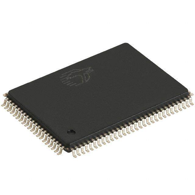
CY7C68013A/CY7C68014A CY7C68015A/CY7C68016A Figure 6. Signal Port GPIF Master Slave FIFO PD7 FD[15] FD[15] PD6 FD[14] FD[14] PD5 FD[13] FD[13] PD4 FD[12] FD[12] PD3 FD[11] FD[11] PD2 FD[10] FD[10] PD1 FD[9] FD[9] PD0 FD[8] FD[8] PB7 FD[7] FD[7] PB6 FD[6] FD[6] PB5 FD[5] FD[5] XTALIN PB4 FD[4] FD[4] XTALOUT PB3 FD[3] FD[3] RESET# PB2 FD[2] FD[2] WAKEUP# PB1 FD[1] FD[1] SCL 56 PB0 FD[0] FD[0] SDA RDY0 SLRD RDY1 SLWR **PE0 replaces IFCLK & PE1 replaces CLKOUT CTL0 FLAGA on CY7C68015A/16A CTL1 FLAGB **PE0 CTL2 FLAGC **PE1 INT0#/PA0 INT0#/PA0 INT0#/ PA0 IFCLK INT1#/PA1 INT1#/PA1 INT1#/ PA1 CLKOUT PA2 PA2 SLOE WU2/PA3 WU2/PA3 WU2/PA3 DPLUS PA4 PA4 FIFOADR0 DMINUS PA5 PA5 FIFOADR1 PA6 PA6 PKTEND PA7 PA7 PA7/FLAGD/SLCS# CTL3 CTL4 CTL5 RDY2 RDY3 100 RDY4 RDY5 BKPT PORTC7/GPIFADR7 PORTC6/GPIFADR6 PORTC5/GPIFADR5 PORTC4/GPIFADR4 RxD0 PORTC3/GPIFADR3 TxD0 PORTC2/GPIFADR2 RxD1 PORTC1/GPIFADR1 TxD1 PORTC0/GPIFADR0 INT4 INT5# PE7/GPIFADR8 PE6/T2EX T2 PE5/INT6 T1 PE4/RxD1OUT T0 PE3/RxD0OUT PE2/T2OUT PE1/T1OUT RD# PE0/T0OUT WR# D7 CS# D6 OE# D5 PSEN# D4 D3 A15 D2 A14 D1 A13 D0 A12 A11 A10 128 A9 A8 A7 A6 A5 A4 EA A3 A2 A1 A0 Document Number: 38-08032 Rev. AC Page 19 of 75
CY7C68013A/CY7C68014A CY7C68015A/CY7C68016A Figure 7. CY7C68013A/CY7C68014A 128-Pin TQFP Pin Assignment 1 1 1 1 1 1 1 1 1 1 1 1 1 1 1 1 1 1 1 1 1 1 1 1 1 1 2 2 2 2 2 2 2 2 2 1 1 1 1 1 1 1 1 1 1 0 0 0 0 0 0 0 8 7 6 5 4 3 2 1 0 9 8 7 6 5 4 3 2 1 0 9 8 7 6 5 4 3 A A A G P P P P A A A A G P P P P P P P P V IN P P P 10 9 8 ND D7/F D6/F D5/F D4/F 7 6 5 4 ND E7/G E6/T E5/IN E4/R E3/R E2/T E1/T E0/T CC T5# D3/F D2/F D1/F 1 CLKOUT D15 D14 D13 D12 PIFA 2EX T6 XD1 XD0 2OU 1OU 0OU D11 D10 D9 PD0/FD8 102 2 VCC D O O T T T *WAKEUP 101 3 GND R8 UT UT VCC 100 4 RDY0/*SLRD RESET# 99 5 RDY1/*SLWR CTL5 98 6 RDY2 A3 97 7 RDY3 A2 96 8 RDY4 A1 95 9 RDY5 A0 94 10 AVCC GND 93 11 XTALOUT PA7/*FLAGD/SLCS# 92 12 XTALIN PA6/*PKTEND 91 13 AGND PA5/FIFOADR1 90 14 NC PA4/FIFOADR0 89 15 NC D7 88 16 NC D6 87 17 AVCC D5 86 18 DPLUS CY7C68013A/CY7C68014A PA3/*WU2 85 19 DMINUS 128-pin TQFP PA2/*SLOE 84 20 AGND PA1/INT1# 83 21 A11 PA0/INT0# 82 22 A12 VCC 81 23 A13 GND 80 24 A14 PC7/GPIFADR7 79 25 A15 PC6/GPIFADR6 78 26 VCC PC5/GPIFADR5 77 27 GND PC4/GPIFADR4 76 28 INT4 PC3/GPIFADR3 75 29 T0 PC2/GPIFADR2 74 30 T1 PC1/GPIFADR1 73 31 T2 PC0/GPIFADR0 72 32 *IFCLK CTL2/*FLAGC 71 33 RESERVED CTL1/*FLAGB 70 34 BKPT CTL0/*FLAGA 69 35 EA VCC 68 36 SCL CTL4 67 37 SDA CTL3 66 38 OE# GND 65 P P P P P P P P P B B B B B B B B S 0 1 2 3 T R T R 4 5 6 7 E R W C V /F /F /F /F V G X X X X /F /F /F /F G V N D R S C D D D D C N D D D D D D D D N D D D D D C # # # # C 0 1 2 3 C D 0 0 1 1 4 5 6 7 D 0 1 2 3 4 C 3 4 4 4 4 4 4 4 4 4 4 5 5 5 5 5 5 5 5 5 5 6 6 6 6 6 9 0 1 2 3 4 5 6 7 8 9 0 1 2 3 4 5 6 7 8 9 0 1 2 3 4 * denotes programmable polarity Document Number: 38-08032 Rev. AC Page 20 of 75
CY7C68013A/CY7C68014A CY7C68015A/CY7C68016A Figure 8. CY7C68013A/CY7C68014A 100-Pin TQFP Pin Assignment 1 9 9 9 9 9 9 9 9 9 9 8 8 8 8 8 8 8 8 8 0 9 8 7 6 5 4 3 2 1 0 9 8 7 6 5 4 3 2 1 0 C G P P P P G P P P P P P P P V IN P P P LKOUT ND D7/FD15 D6/FD14 D5/FD13 D4/FD12 ND E7/GPIFA E6/T2EX E5/INT6 E4/RXD1 E3/RXD0 E2/T2OU E1/T1OU E0/T0OU CC T5# D3/FD11 D2/FD10 D1/FD9 O O T T T D R U U 8 T T 1 VCC PD0/FD8 80 2 GND *WAKEUP 79 3 RDY0/*SLRD VCC 78 4 RDY1/*SLWR RESET# 77 5 RDY2 CTL5 76 6 RDY3 GND 75 7 RDY4 PA7/*FLAGD/SLCS# 74 8 RDY5 PA6/*PKTEND 73 9 AVCC PA5/FIFOADR1 72 10 XTALOUT PA4/FIFOADR0 71 11 XTALIN PA3/*WU2 70 12 AGND PA2/*SLOE 69 13 NC PA1/INT1# 68 14 NC PA0/INT0# 67 15 NC CY7C68013A/CY7C68014A VCC 66 16 AVCC 100-pin TQFP GND 65 17 DPLUS PC7/GPIFADR7 64 18 DMINUS PC6/GPIFADR6 63 19 AGND PC5/GPIFADR5 62 20 VCC PC4/GPIFADR4 61 21 GND PC3/GPIFADR3 60 22 INT4 PC2/GPIFADR2 59 23 T0 PC1/GPIFADR1 58 24 T1 PC0/GPIFADR0 57 25 T2 CTL2/*FLAGC 56 26 *IFCLK CTL1/*FLAGB 55 27 RESERVED CTL0/*FLAGA 54 28 BKPT VCC 53 29 SCL CTL4 52 30 SDA CTL3 51 P P P P P P P P B B B B B B B B 0 1 2 3 T R T R 4 5 6 7 R W V /F /F /F /F V G X X X X /F /F /F /F G V G D R C D D D D C N D D D D D D D D N C N # # C 0 1 2 3 C D 0 0 1 1 4 5 6 7 D C D 3 3 3 3 3 3 3 3 3 4 4 4 4 4 4 4 4 4 4 5 1 2 3 4 5 6 7 8 9 0 1 2 3 4 5 6 7 8 9 0 * denotes programmable polarity Document Number: 38-08032 Rev. AC Page 21 of 75
CY7C68013A/CY7C68014A CY7C68015A/CY7C68016A Figure 9. CY7C68013A/CY7C68014A 56-Pin SSOP Pin Assignment CY7C68013A/CY7C68014A 56-pin SSOP 1 PD5/FD13 PD4/FD12 56 2 PD6/FD14 PD3/FD11 55 3 PD7/FD15 PD2/FD10 54 4 GND PD1/FD9 53 5 CLKOUT PD0/FD8 52 6 VCC *WAKEUP 51 7 GND VCC 50 8 RDY0/*SLRD RESET# 49 9 RDY1/*SLWR GND 48 10 AVCC PA7/*FLAGD/SLCS# 47 11 XTALOUT PA6/PKTEND 46 12 XTALIN PA5/FIFOADR1 45 13 AGND PA4/FIFOADR0 44 14 AVCC PA3/*WU2 43 15 DPLUS PA2/*SLOE 42 16 DMINUS PA1/INT1# 41 17 AGND PA0/INT0# 40 18 VCC VCC 39 19 GND CTL2/*FLAGC 38 20 *IFCLK CTL1/*FLAGB 37 21 RESERVED CTL0/*FLAGA 36 22 SCL GND 35 23 SDA VCC 34 24 VCC GND 33 25 PB0/FD0 PB7/FD7 32 26 PB1/FD1 PB6/FD6 31 27 PB2/FD2 PB5/FD5 30 28 PB3/FD3 PB4/FD4 29 * denotes programmable polarity Document Number: 38-08032 Rev. AC Page 22 of 75
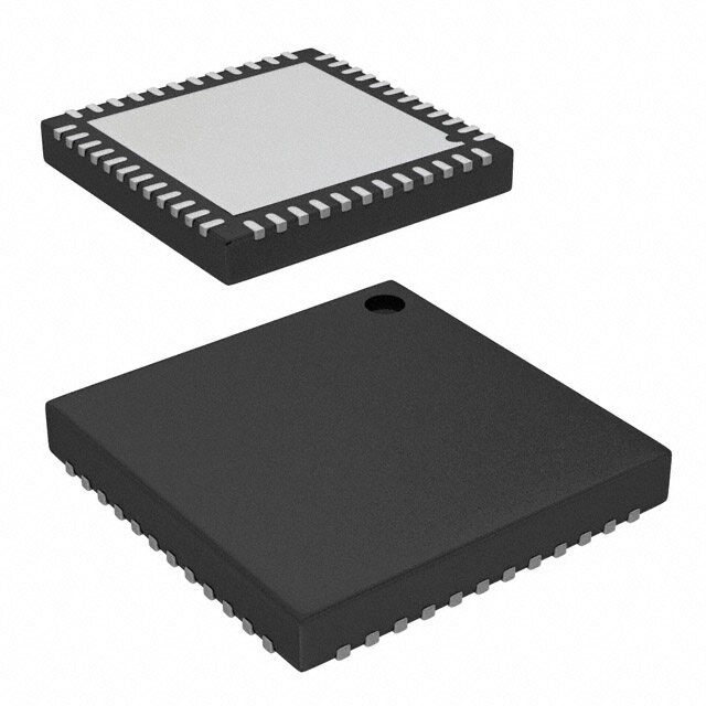
CY7C68013A/CY7C68014A CY7C68015A/CY7C68016A Figure 10. CY7C68013A/14A/15A/16A 56-Pin QFN Pin Assignment C L K O P P P P P P * U D D D D D D P P W T 7 6 5 4 3 2 D D A G V /**P G /FD /FD /FD /FD /FD /FD 1/F 0/F KE V N C E N 1 1 1 1 1 1 D D U C D C 1 D 5 4 3 2 1 0 9 8 P C 5 5 5 5 5 5 5 4 4 4 4 4 4 4 6 5 4 3 2 1 0 9 8 7 6 5 4 3 RDY0/*SLRD 1 42 RESET# RDY1/*SLWR 2 41 GND AVCC 3 40 PA7/*FLAGD/SLCS# XTALOUT 4 39 PA6/*PKTEND XTALIN 5 CY7C68013A/CY7C68014A 38 PA5/FIFOADR1 & AGND 6 CY7C68015A/CY7C68016A 37 PA4/FIFOADR0 AVCC 7 36 PA3/*WU2 56-pin QFN DPLUS 8 35 PA2/*SLOE DMINUS 9 34 PA1/INT1# AGND 10 33 PA0/INT0# VCC 11 32 VCC GND 12 31 CTL2/*FLAGC *IFCLK/**PE0 13 30 CTL1/*FLAGB RESERVED 14 29 CTL0/*FLAGA 1 1 1 1 1 2 2 2 2 2 2 2 2 2 5 6 7 8 9 0 1 2 3 4 5 6 7 8 S S V P P P P P P P P G V G C D C B B B B B B B B N C N L A C 0 1 2 3 4 5 6 7 D C D /F /F /F /F /F /F /F /F D D D D D D D D 0 1 2 3 4 5 6 7 * denotes programmable polarity ** denotes CY7C68015A/CY7C68016A pinout Document Number: 38-08032 Rev. AC Page 23 of 75
CY7C68013A/CY7C68014A CY7C68015A/CY7C68016A Figure 11. CY7C68013A 56-pin VFBGA Pin Assignment – Top View 1 2 3 4 5 6 7 8 A 1A 2A 3A 4A 5A 6A 7A 8A B 1B 2B 3B 4B 5B 6B 7B 8B C 1C 2C 3C 4C 5C 6C 7C 8C D 1D 2D 7D 8D E 1E 2E 7E 8E F 1F 2F 3F 4F 5F 6F 7F 8F G 1G 2G 3G 4G 5G 6G 7G 8G H 1H 2H 3H 4H 5H 6H 7H 8H Document Number: 38-08032 Rev. AC Page 24 of 75
CY7C68013A/CY7C68014A CY7C68015A/CY7C68016A CY7C68013A/15A Pin Descriptions Table 11. FX2LP Pin Descriptions[13] 128 100 56 56 56 Name Type Default Reset[14] Description TQFP TQFP SSOP QFN VFBGA Analog VCC. Connect this pin to the 3.3V power 10 9 10 3 2D AVCC Power N/A N/A source. This signal provides power to the analog section of the chip. Analog VCC. Connect this pin to the 3.3V power 17 16 14 7 1D AVCC Power N/A N/A source. This signal provides power to the analog section of the chip. Analog Ground. Connect to ground with as short 13 12 13 6 2F AGND Ground N/A N/A a path as possible. Analog Ground. Connect to ground with as short 20 19 17 10 1F AGND Ground N/A N/A a path as possible. 19 18 16 9 1E DMINUS I/O/Z Z N/A USB D– Signal. Connect to the USB D– signal. 18 17 15 8 2E DPLUS I/O/Z Z N/A USB D+ Signal. Connect to the USB D+ signal. 94 – – – – A0 Output L L 95 – – – – A1 Output L L 96 – – – – A2 Output L L 97 – – – – A3 Output L L 117 – – – – A4 Output L L 118 – – – – A5 Output L L 119 – – – – A6 Output L L 120 – – – – A7 Output L L 8051 Address Bus. This bus is driven at all times. When the 8051 is addressing internal RAM it 126 – – – – A8 Output L L reflects the internal address. 127 – – – – A9 Output L L 128 – – – – A10 Output L L 21 – – – – A11 Output L L 22 – – – – A12 Output L L 23 – – – – A13 Output L L 24 – – – – A14 Output L L 25 – – – – A15 Output L L 59 – – – – D0 I/O/Z Z Z 60 – – – – D1 I/O/Z Z Z 8051 Data Bus. This bidirectional bus is 61 – – – – D2 I/O/Z Z Z highimpedance when inactive, input for bus reads, 62 – – – – D3 I/O/Z Z Z and output for bus writes. The data bus is used for 63 – – – – D4 I/O/Z Z Z external 8051 program and data memory. The data bus is active only for external bus accesses, and is 86 – – – – D5 I/O/Z Z Z driven LOW in suspend. 87 – – – – D6 I/O/Z Z Z 88 – – – – D7 I/O/Z Z Z Program Store Enable. This active LOW signal indicates an 8051 code fetch from external 39 – – – – PSEN# Output H H memory. It is active for program memory fetches from 0x4000–0xFFFF when the EA pin is LOW, or from 0x0000–0xFFFF when the EA pin is HIGH. Notes 13.Unused inputs must not be left floating. Tie either HIGH or LOW as appropriate. Outputs should only be pulled up or down to ensure signals at power up and in standby. Note also that no pins should be driven while the device is powered down. 14.The Reset column indicates the state of signals during reset (RESET# asserted) or during Power on Reset (POR). Document Number: 38-08032 Rev. AC Page 25 of 75
CY7C68013A/CY7C68014A CY7C68015A/CY7C68016A Table 11. FX2LP Pin Descriptions[13] (continued) 128 100 56 56 56 Name Type Default Reset[14] Description TQFP TQFP SSOP QFN VFBGA Breakpoint. This pin goes active (HIGH) when the 8051 address bus matches the BPADDRH/L registers and breakpoints are enabled in the BREAKPT register (BPEN = 1). If the BPPULSE bit 34 28 – – BKPT Output L L in the BREAKPT register is HIGH, this signal pulses HIGH for eight 12-/24-/48-MHz clocks. If the BPPULSE bit is LOW, the signal remains HIGH until the 8051 clears the BREAK bit (by writing 1 to it) in the BREAKPT register. Active LOW Reset. Resets the entire chip. See 99 77 49 42 8B RESET# Input N/A N/A section ”Reset and Wakeup”on page9 for more details. External Access. This pin determines where the 8051 fetches code between addresses 0x0000 and 35 – – – – EA Input N/A N/A 0x3FFF. If EA = 0 the 8051 fetches this code from its internal RAM. IF EA = 1 the 8051 fetches this code from external memory. Crystal Input. Connect this signal to a 24-MHz parallel-resonant, fundamental mode crystal and load capacitor to GND. 12 11 12 5 1C XTALIN Input N/A N/A It is also correct to drive XTALIN with an external 24-MHz square wave derived from another clock source. When driving from an external source, the driving signal should be a 3.3-V square wave. Crystal Output. Connect this signal to a 24-MHz parallel-resonant, fundamental mode crystal and 11 10 11 4 2C XTALOUT Output N/A N/A load capacitor to GND. If an external clock is used to drive XTALIN, leave this pin open. CLKOUT on Clock CY7C68013A O/Z 12 MHz CLKOUT: 12-, 24- or 48-MHz clock, phase-locked Driven and to the 24-MHz input clock. The 8051 defaults to CY7C68014A 12-MHz operation. The 8051 may three-state this 1 100 5 54 2B ------------------ output by setting CPUCS.1 = 1. ---------- PE1 on ---------- ---------- ------------------------------------------------------------------ Z CY7C68015A - I ------PE1 is a bidirectional I/O port pin. and I/O/Z CY7C68016A Port A Multiplexed pin whose function is selected by PORTACFG.0 Z PA0 or I PA0 is a bidirectional I/O port pin. 82 67 40 33 8G I/O/Z (PA0) INT0# (PA0) INT0# is the active-LOW 8051 INT0 interrupt input signal, which is either edge-triggered (IT0 = 1) or level-triggered (IT0 = 0). Multiplexed pin whose function is selected by: PORTACFG.1 PA1 or I Z PA1 is a bidirectional I/O port pin. 83 68 41 34 6G I/O/Z INT1# (PA1) (PA1) INT1# is the active-LOW 8051 INT1 interrupt input signal, which is either edge-triggered (IT1 = 1) or level-triggered (IT1 = 0). Document Number: 38-08032 Rev. AC Page 26 of 75
CY7C68013A/CY7C68014A CY7C68015A/CY7C68016A Table 11. FX2LP Pin Descriptions[13] (continued) 128 100 56 56 56 Name Type Default Reset[14] Description TQFP TQFP SSOP QFN VFBGA Multiplexed pin whose function is selected by two bits: Z IFCONFIG[1:0]. PA2 or I 84 69 42 35 8F I/O/Z (PA2) PA2 is a bidirectional I/O port pin. SLOE (PA2) SLOE is an input-only output enable with program- mable polarity (FIFOPINPOLAR.4) for the slave FIFOs connected to FD[7..0] or FD[15..0]. Multiplexed pin whose function is selected by: WAKEUP.7 and OEA.3 PA3 is a bidirectional I/O port pin. WU2 is an alternate source for USB Wakeup, PA3 or I Z enabled by WU2EN bit (WAKEUP.1) and polarity 85 70 43 36 7F I/O/Z WU2 (PA3) (PA3) set by WU2POL (WAKEUP.4). If the 8051 is in suspend and WU2EN = 1, a transition on this pin starts up the oscillator and interrupts the 8051 to enable it to exit the suspend mode. Asserting this pin inhibits the chip from suspending if WU2EN = 1. Multiplexed pin whose function is selected by: IFCONFIG[1..0]. PA4 or I Z 89 71 44 37 6F I/O/Z PA4 is a bidirectional I/O port pin. FIFOADR0 (PA4) (PA4) FIFOADR0 is an input-only address select for the slave FIFOs connected to FD[7..0] or FD[15..0]. Multiplexed pin whose function is selected by: IFCONFIG[1..0]. PA5 or I Z 90 72 45 38 8C I/O/Z PA5 is a bidirectional I/O port pin. FIFOADR1 (PA5) (PA5) FIFOADR1 is an input-only address select for the slave FIFOs connected to FD[7..0] or FD[15..0]. Multiplexed pin whose function is selected by the IFCONFIG[1:0] bits. PA6 or I Z PA6 is a bidirectional I/O port pin. 91 73 46 39 7C I/O/Z PKTEND (PA6) (PA6) PKTEND is an input used to commit the FIFO packet data to the endpoint and whose polarity is programmable via FIFOPINPOLAR.5. Multiplexed pin whose function is selected by the IFCONFIG[1:0] and PORTACFG.7 bits. PA7 or I Z PA7 is a bidirectional I/O port pin. 92 74 47 40 6C FLAGD or I/O/Z (PA7) (PA7) FLAGD is a programmable slave-FIFO output SLCS# status flag signal. SLCS# gates all other slave FIFO enable/strobes Port B Multiplexed pin whose function is selected by the Z PB0 or I following bits: IFCONFIG[1..0]. 44 34 25 18 3H I/O/Z (PB0) FD[0] (PB0) PB0 is a bidirectional I/O port pin. FD[0] is the bidirectional FIFO/GPIF data bus. Multiplexed pin whose function is selected by the PB1 or I Z following bits: IFCONFIG[1..0]. 45 35 26 19 4F I/O/Z FD[1] (PB1) (PB1) PB1 is a bidirectional I/O port pin. FD[1] is the bidirectional FIFO/GPIF data bus. Multiplexed pin whose function is selected by the PB2 or I Z following bits: IFCONFIG[1..0]. 46 36 27 20 4H I/O/Z FD[2] (PB2) (PB2) PB2 is a bidirectional I/O port pin. FD[2] is the bidirectional FIFO/GPIF data bus. Document Number: 38-08032 Rev. AC Page 27 of 75
CY7C68013A/CY7C68014A CY7C68015A/CY7C68016A Table 11. FX2LP Pin Descriptions[13] (continued) 128 100 56 56 56 Name Type Default Reset[14] Description TQFP TQFP SSOP QFN VFBGA Multiplexed pin whose function is selected by the PB3 or I Z following bits: IFCONFIG[1..0]. 47 37 28 21 4G I/O/Z FD[3] (PB3) (PB3) PB3 is a bidirectional I/O port pin. FD[3] is the bidirectional FIFO/GPIF data bus. Multiplexed pin whose function is selected by the PB4 or I Z following bits: IFCONFIG[1..0]. 54 44 29 22 5H I/O/Z FD[4] (PB4) (PB4) PB4 is a bidirectional I/O port pin. FD[4] is the bidirectional FIFO/GPIF data bus. Multiplexed pin whose function is selected by the PB5 or I Z following bits: IFCONFIG[1..0]. 55 45 30 23 5G I/O/Z FD[5] (PB5) (PB5) PB5 is a bidirectional I/O port pin. FD[5] is the bidirectional FIFO/GPIF data bus. Multiplexed pin whose function is selected by the PB6 or I Z following bits: IFCONFIG[1..0]. 56 46 31 24 5F I/O/Z FD[6] (PB6) (PB6) PB6 is a bidirectional I/O port pin. FD[6] is the bidirectional FIFO/GPIF data bus. Multiplexed pin whose function is selected by the PB7 or I Z following bits: IFCONFIG[1..0]. 57 47 32 25 6H I/O/Z FD[7] (PB7) (PB7) PB7 is a bidirectional I/O port pin. FD[7] is the bidirectional FIFO/GPIF data bus. PORT C Multiplexed pin whose function is selected by Z PC0 or I PORTCCFG.0 72 57 – – – I/O/Z (PC0) GPIFADR0 (PC0) PC0 is a bidirectional I/O port pin. GPIFADR0 is a GPIF address output pin. Multiplexed pin whose function is selected by PC1 or Z I PORTCCFG.1 73 58 – – – GPIFADR1 I/O/Z (PC1) (PC1) PC1 is a bidirectional I/O port pin. GPIFADR1 is a GPIF address output pin. Multiplexed pin whose function is selected by PC2 or I Z PORTCCFG.2 74 59 – – – I/O/Z GPIFADR2 (PC2) (PC2) PC2 is a bidirectional I/O port pin. GPIFADR2 is a GPIF address output pin. Multiplexed pin whose function is selected by PC3 or I Z PORTCCFG.3 75 60 – – – GPIFADR3 I/O/Z (PC3) (PC3) PC3 is a bidirectional I/O port pin. GPIFADR3 is a GPIF address output pin. Multiplexed pin whose function is selected by PC4 or I Z PORTCCFG.4 76 61 – – – GPIFADR4 I/O/Z (PC4) (PC4) PC4 is a bidirectional I/O port pin. GPIFADR4 is a GPIF address output pin. Multiplexed pin whose function is selected by PC5 or I Z PORTCCFG.5 77 62 – – – GPIFADR5 I/O/Z (PC5) (PC5) PC5 is a bidirectional I/O port pin. GPIFADR5 is a GPIF address output pin. Multiplexed pin whose function is selected by PC6 or I Z PORTCCFG.6 78 63 – – – GPIFADR6 I/O/Z (PC6) (PC6) PC6 is a bidirectional I/O port pin. GPIFADR6 is a GPIF address output pin. Multiplexed pin whose function is selected by PC7 or I Z PORTCCFG.7 79 64 – – – I/O/Z GPIFADR7 (PC7) (PC7) PC7 is a bidirectional I/O port pin. GPIFADR7 is a GPIF address output pin. Document Number: 38-08032 Rev. AC Page 28 of 75
CY7C68013A/CY7C68014A CY7C68015A/CY7C68016A Table 11. FX2LP Pin Descriptions[13] (continued) 128 100 56 56 56 Name Type Default Reset[14] Description TQFP TQFP SSOP QFN VFBGA PORT D Multiplexed pin whose function is selected by the PD0 or I Z IFCONFIG[1..0] and EPxFIFOCFG.0 (wordwide) 102 80 52 45 8A I/O/Z FD[8] (PD0) (PD0) bits. FD[8] is the bidirectional FIFO/GPIF data bus. Multiplexed pin whose function is selected by the PD1 or I Z IFCONFIG[1..0] and EPxFIFOCFG.0 (wordwide) 103 81 53 46 7A I/O/Z FD[9] (PD1) (PD1) bits. FD[9] is the bidirectional FIFO/GPIF data bus. Multiplexed pin whose function is selected by the PD2 or I Z IFCONFIG[1..0] and EPxFIFOCFG.0 (wordwide) 104 82 54 47 6B I/O/Z FD[10] (PD2) (PD2) bits. FD[10] is the bidirectional FIFO/GPIF data bus. Multiplexed pin whose function is selected by the PD3 or I Z IFCONFIG[1..0] and EPxFIFOCFG.0 (wordwide) 105 83 55 48 6A I/O/Z FD[11] (PD3) (PD3) bits. FD[11] is the bidirectional FIFO/GPIF data bus. Multiplexed pin whose function is selected by the PD4 or I Z IFCONFIG[1..0] and EPxFIFOCFG.0 (wordwide) 121 95 56 49 3B I/O/Z FD[12] (PD4) (PD4) bits. FD[12] is the bidirectional FIFO/GPIF data bus. Multiplexed pin whose function is selected by the PD5 or I Z IFCONFIG[1..0] and EPxFIFOCFG.0 (wordwide) 122 96 1 50 3A I/O/Z FD[13] (PD5) (PD5) bits. FD[13] is the bidirectional FIFO/GPIF data bus. Multiplexed pin whose function is selected by the PD6 or I Z IFCONFIG[1..0] and EPxFIFOCFG.0 (wordwide) 123 97 2 51 3C I/O/Z FD[14] (PD6) (PD6) bits. FD[14] is the bidirectional FIFO/GPIF data bus. Multiplexed pin whose function is selected by the PD7 or I Z IFCONFIG[1..0] and EPxFIFOCFG.0 (wordwide) 124 98 3 52 2A I/O/Z FD[15] (PD7) (PD7) bits. FD[15] is the bidirectional FIFO/GPIF data bus. Port E Multiplexed pin whose function is selected by the PORTECFG.0 bit. PE0 is a bidirectional I/O port pin. T0OUT is an active-HIGH signal from 8051 PE0 or I Z 108 86 – – – I/O/Z Timer-counter0. T0OUT outputs a high level for T0OUT (PE0) (PE0) one CLKOUT clock cycle when Timer0 overflows. If Timer0 is operated in Mode 3 (two separate timer/counters), T0OUT is active when the low byte timer/counter overflows. Multiplexed pin whose function is selected by the PORTECFG.1 bit. PE1 is a bidirectional I/O port pin. T1OUT is an active HIGH signal from 8051 PE1 or I Z 109 87 – – – I/O/Z Timer-counter1. T1OUT outputs a high level for T1OUT (PE1) (PE1) one CLKOUT clock cycle when Timer1 overflows. If Timer1 is operated in Mode 3 (two separate timer/counters), T1OUT is active when the low byte timer/counter overflows. Document Number: 38-08032 Rev. AC Page 29 of 75
CY7C68013A/CY7C68014A CY7C68015A/CY7C68016A Table 11. FX2LP Pin Descriptions[13] (continued) 128 100 56 56 56 Name Type Default Reset[14] Description TQFP TQFP SSOP QFN VFBGA Multiplexed pin whose function is selected by the PORTECFG.2 bit. PE2 or I Z PE2 is a bidirectional I/O port pin. 110 88 – – – I/O/Z T2OUT (PE2) (PE2) T2OUT is the active HIGH output signal from 8051 Timer2. T2OUT is active (HIGH) for one clock cycle when Timer/Counter 2 overflows. Multiplexed pin whose function is selected by the PORTECFG.3 bit. PE3 is a bidirectional I/O port pin. PE3 or I Z RXD0OUT is an active HIGH signal from 8051 111 89 – – – I/O/Z RXD0OUT (PE3) (PE3) UART0. If RXD0OUT is selected and UART0 is in Mode 0, this pin provides the output data for UART0 only when it is in sync mode. Otherwise it is a 1. Multiplexed pin whose function is selected by the PORTECFG.4 bit. PE4 is a bidirectional I/O port pin. PE4 or I Z RXD1OUT is an active-HIGH output from 8051 112 90 – – – I/O/Z RXD1OUT (PE4) (PE4) UART1. When RXD1OUT is selected and UART1 is in Mode 0, this pin provides the output data for UART1 only when it is in sync mode. In Modes 1, 2, and 3, this pin is HIGH. Multiplexed pin whose function is selected by the PORTECFG.5 bit. PE5 or I Z PE5 is a bidirectional I/O port pin. 113 91 – – – I/O/Z INT6 (PE5) (PE5) INT6 is the 8051 INT6 interrupt request input signal. The INT6 pin is edge-sensitive, active HIGH. Multiplexed pin whose function is selected by the PORTECFG.6 bit. PE6 is a bidirectional I/O port pin. PE6 or I Z 114 92 – – – I/O/Z T2EX is an active HIGH input signal to the 8051 T2EX (PE6) (PE6) Timer2. T2EX reloads timer 2 on its falling edge. T2EX is active only if the EXEN2 bit is set in T2CON. Multiplexed pin whose function is selected by the PE7 or I Z PORTECFG.7 bit. 115 93 – – – I/O/Z GPIFADR8 (PE7) (PE7) PE7 is a bidirectional I/O port pin. GPIFADR8 is a GPIF address output pin. Multiplexed pin whose function is selected by the following bits: IFCONFIG[1..0]. RDY0 or 4 3 8 1 1A Input N/A N/A RDY0 is a GPIF input signal. SLRD SLRD is the input-only read strobe with program- mable polarity (FIFOPINPOLAR.3) for the slave FIFOs connected to FD[7..0] or FD[15..0]. Multiplexed pin whose function is selected by the following bits: IFCONFIG[1..0]. RDY1 or 5 4 9 2 1B Input N/A N/A RDY1 is a GPIF input signal. SLWR SLWR is the input-only write strobe with program- mable polarity (FIFOPINPOLAR.2) for the slave FIFOs connected to FD[7..0] or FD[15..0]. 6 5 – – – RDY2 Input N/A N/A RDY2 is a GPIF input signal. Document Number: 38-08032 Rev. AC Page 30 of 75
CY7C68013A/CY7C68014A CY7C68015A/CY7C68016A Table 11. FX2LP Pin Descriptions[13] (continued) 128 100 56 56 56 Name Type Default Reset[14] Description TQFP TQFP SSOP QFN VFBGA 7 6 – – – RDY3 Input N/A N/A RDY3 is a GPIF input signal. 8 7 – – – RDY4 Input N/A N/A RDY4 is a GPIF input signal. 9 8 – – – RDY5 Input N/A N/A RDY5 is a GPIF input signal. Multiplexed pin whose function is selected by the following bits: IFCONFIG[1..0]. CTL0 or CTL0 is a GPIF control output. 69 54 36 29 7H O/Z H L FLAGA FLAGA is a programmable slave-FIFO output status flag signal. Defaults to programmable for the FIFO selected by the FIFOADR[1:0] pins. Multiplexed pin whose function is selected by the following bits: IFCONFIG[1..0]. CTL1 or CTL1 is a GPIF control output. 70 55 37 30 7G O/Z H L FLAGB FLAGB is a programmable slave-FIFO output status flag signal. Defaults to FULL for the FIFO selected by the FIFOADR[1:0] pins. Multiplexed pin whose function is selected by the following bits: IFCONFIG[1..0]. CTL2 or CTL2 is a GPIF control output. 71 56 38 31 8H O/Z H L FLAGC FLAGC is a programmable slave-FIFO output status flag signal. Defaults to EMPTY for the FIFO selected by the FIFOADR[1:0] pins. 66 51 – – – CTL3 O/Z H L CTL3 is a GPIF control output. 67 52 – – – CTL4 Output H L CTL4 is a GPIF control output. 98 76 – – – CTL5 Output H L CTL5 is a GPIF control output. IFCLK on Interface Clock, used for synchronously clocking CY7C68013A I/O/Z Z Z data into or out of the slave FIFOs. IFCLK also and serves as a timing reference for all slave FIFO CY7C68014A control signals and GPIF. When internal clocking is used (IFCONFIG.7=1) the IFCLK pin can be configured to output 30/48 MHz by bits 32 26 20 13 2G IFCONFIG.5 and IFCONFIG.6. IFCLK may be inverted, whether internally or externally sourced, ------------------ by setting the bit IFCONFIG.4 =1. PE0 on ---------- ---------- ---------- ------------------------------------------------------------------ CY7C68015A – I Z ----- and I/O/Z PE0 is a bidirectional I/O port pin. CY7C68016A INT4 is the 8051 INT4 interrupt request input 28 22 – – – INT4 Input N/A N/A signal. The INT4 pin is edge-sensitive, active HIGH. INT5# is the 8051 INT5 interrupt request input 106 84 – – – INT5# Input N/A N/A signal. The INT5 pin is edge-sensitive, active LOW. T2 is the active HIGH T2 input signal to 8051 Timer2, which provides the input to Timer2 when 31 25 – – – T2 Input N/A N/A C/T2 = 1. When C/T2 = 0, Timer2 does not use this pin. Document Number: 38-08032 Rev. AC Page 31 of 75
CY7C68013A/CY7C68014A CY7C68015A/CY7C68016A Table 11. FX2LP Pin Descriptions[13] (continued) 128 100 56 56 56 Name Type Default Reset[14] Description TQFP TQFP SSOP QFN VFBGA T1 is the active HIGH T1 signal for 8051 Timer1, 30 24 – – – T1 Input N/A N/A which provides the input to Timer1 when C/T1 is 1. When C/T1 is 0, Timer1 does not use this bit. T0 is the active HIGH T0 signal for 8051 Timer0, 29 23 – – – T0 Input N/A N/A which provides the input to Timer0 when C/T0 is 1. When C/T0 is 0, Timer0 does not use this bit. RXD1is an active HIGH input signal for 8051 53 43 – – – RXD1 Input N/A N/A UART1, which provides data to the UART in all modes. TXD1is an active HIGH output pin from 8051 52 42 – – – TXD1 Output H L UART1, which provides the output clock in sync mode, and the output data in async mode. RXD0 is the active HIGH RXD0 input to 8051 51 41 – – – RXD0 Input N/A N/A UART0, which provides data to the UART in all modes. TXD0 is the active HIGH TXD0 output from 8051 50 40 – – – TXD0 Output H L UART0, which provides the output clock in sync mode, and the output data in async mode. CS# is the active LOW chip select for external 42 – – – CS# Output H H memory. WR# is the active LOW write strobe output for 41 32 – – – WR# Output H H external memory. RD# is the active LOW read strobe output for 40 31 – – – RD# Output H H external memory. OE# is the active LOW output enable for external 38 – – – OE# Output H H memory. 33 27 21 14 2H Reserved Input N/A N/A Reserved. Connect to ground. USB Wakeup. If the 8051 is in suspend, asserting this pin starts up the oscillator and interrupts the 8051 to enable it to exit the suspend mode. Holding 101 79 51 44 7B WAKEUP Input N/A N/A WAKEUP asserted inhibits the EZ-USB chip from suspending. This pin has programmable polarity (WAKEUP.4). Z Clock for the I2C interface. Connect to VCC with a 36 29 22 15 3F SCL OD Z (if 2.2-k resistor, even if no I2C peripheral is booting attached. is done) Z Data for I2C compatible interface. Connect to 37 30 23 16 3G SDA OD Z (if VCC with a 2.2-k resistor, even if no I2C booting compatible peripheral is attached. is done) 2 1 6 55 5A VCC Power N/A N/A VCC. Connect to the 3.3-V power source. 26 20 18 11 1G VCC Power N/A N/A VCC. Connect to the 3.3-V power source. 43 33 24 17 7E VCC Power N/A N/A VCC. Connect to the 3.3-V power source. 48 38 – – – VCC Power N/A N/A VCC. Connect to 3.3-V power source. 64 49 34 27 8E VCC Power N/A N/A VCC. Connect to the 3.3-V power source. 68 53 – – – VCC Power N/A N/A VCC. Connect to the 3.3-V power source. 81 66 39 32 5C VCC Power N/A N/A VCC. Connect to the 3.3-V power source. Document Number: 38-08032 Rev. AC Page 32 of 75
CY7C68013A/CY7C68014A CY7C68015A/CY7C68016A Table 11. FX2LP Pin Descriptions[13] (continued) 128 100 56 56 56 Name Type Default Reset[14] Description TQFP TQFP SSOP QFN VFBGA 100 78 50 43 5B VCC Power N/A N/A VCC. Connect to the 3.3-V power source. 107 85 – – – VCC Power N/A N/A VCC. Connect to the 3.3-V power source. 3 2 7 56 4B GND Ground N/A N/A Ground 27 21 19 12 1H GND Ground N/A N/A Ground 49 39 – – – GND Ground N/A N/A Ground 58 48 33 26 7D GND Ground N/A N/A Ground 65 50 35 28 8D GND Ground N/A N/A Ground 80 65 – – – GND Ground N/A N/A Ground 93 75 48 41 4C GND Ground N/A N/A Ground 116 94 – – – GND Ground N/A N/A Ground 125 99 4 53 4A GND Ground N/A N/A Ground 14 13 – – – NC N/A N/A N/A No Connect. This pin must be left open. 15 14 – – – NC N/A N/A N/A No Connect. This pin must be left open. 16 15 – – – NC N/A N/A N/A No Connect. This pin must be left open. Document Number: 38-08032 Rev. AC Page 33 of 75
CY7C68013A/CY7C68014A CY7C68015A/CY7C68016A Register Summary FX2LP register bit definitions are described in the FX2LP TRM in greater detail. Table 12. FX2LP Register Summary Hex Size Name Description b7 b6 b5 b4 b3 b2 b1 b0 Default Access GPIF Waveform Memories E400 128 WAVEDATA GPIF Waveform D7 D6 D5 D4 D3 D2 D1 D0 xxxxxxxx RW Descriptor 0, 1, 2, 3 data E480 128 reserved GENERAL CONFIGURATION E50D GPCR2 General Purpose Configu-reserved reserved reserved FULL_SPEEreserved reserved reserved reserved 00000000R ration Register 2 D_ONLY E600 1 CPUCS CPU Control & Status 0 0 PORTCSTB CLKSPD1 CLKSPD0 CLKINV CLKOE 8051RES 00000010rrbbbbbr E601 1 IFCONFIG Interface Configuration IFCLKSRC 3048MHZ IFCLKOE IFCLKPOL ASYNC GSTATE IFCFG1 IFCFG0 10000000RW (Ports, GPIF, slave FIFOs) E602 1 PINFLAGSAB[15] Slave FIFO FLAGA and FLAGB3 FLAGB2 FLAGB1 FLAGB0 FLAGA3 FLAGA2 FLAGA1 FLAGA0 00000000RW FLAGB Pin Configuration E603 1 PINFLAGSCD[15] Slave FIFO FLAGC and FLAGD3 FLAGD2 FLAGD1 FLAGD0 FLAGC3 FLAGC2 FLAGC1 FLAGC0 00000000RW FLAGD Pin Configuration E604 1 FIFORESET[15] Restore FIFOS to default NAKALL 0 0 0 EP3 EP2 EP1 EP0 xxxxxxxx W state E605 1 BREAKPT Breakpoint Control 0 0 0 0 BREAK BPPULSE BPEN 0 00000000rrrrbbbr E606 1 BPADDRH Breakpoint Address H A15 A14 A13 A12 A11 A10 A9 A8 xxxxxxxx RW E607 1 BPADDRL Breakpoint Address L A7 A6 A5 A4 A3 A2 A1 A0 xxxxxxxx RW E608 1 UART230 230 Kbaud internally 0 0 0 0 0 0 230UART1 230UART0 00000000rrrrrrbb generated ref. clock E609 1 FIFOPINPOLAR[15] Slave FIFO Interface pins 0 0 PKTEND SLOE SLRD SLWR EF FF 00000000rrbbbbbb polarity E60A 1 REVID Chip Revision rv7 rv6 rv5 rv4 rv3 rv2 rv1 rv0 RevA R 00000001 E60B 1 REVCTL[15] Chip Revision Control 0 0 0 0 0 0 dyn_out enh_pkt 00000000rrrrrrbb UDMA E60C 1 GPIFHOLDAMOUNT MSTB Hold Time 0 0 0 0 0 0 HOLDTIME1HOLDTIME0 00000000rrrrrrbb (for UDMA) 3 reserved ENDPOINT CONFIGURATION E610 1 EP1OUTCFG Endpoint 1-OUT VALID 0 TYPE1 TYPE0 0 0 0 0 10100000brbbrrrr Configuration E611 1 EP1INCFG Endpoint 1-IN VALID 0 TYPE1 TYPE0 0 0 0 0 10100000brbbrrrr Configuration E612 1 EP2CFG Endpoint 2 Configuration VALID DIR TYPE1 TYPE0 SIZE 0 BUF1 BUF0 10100010bbbbbrbb E613 1 EP4CFG Endpoint 4 Configuration VALID DIR TYPE1 TYPE0 0 0 0 0 10100000bbbbrrrr E614 1 EP6CFG Endpoint 6 Configuration VALID DIR TYPE1 TYPE0 SIZE 0 BUF1 BUF0 11100010 bbbbbrbb E615 1 EP8CFG Endpoint 8 Configuration VALID DIR TYPE1 TYPE0 0 0 0 0 11100000 bbbbrrrr 2 reserved E618 1 EP2FIFOCFG[15] Endpoint 2 / slave FIFO 0 INFM1 OEP1 AUTOOUT AUTOIN ZEROLENIN0 WORDWIDE 00000101rbbbbbrb configuration E619 1 EP4FIFOCFG[15] Endpoint 4 / slave FIFO 0 INFM1 OEP1 AUTOOUT AUTOIN ZEROLENIN0 WORDWIDE 00000101rbbbbbrb configuration E61A 1 EP6FIFOCFG[15] Endpoint 6 / slave FIFO 0 INFM1 OEP1 AUTOOUT AUTOIN ZEROLENIN0 WORDWIDE 00000101rbbbbbrb configuration E61B 1 EP8FIFOCFG[15] Endpoint 8 / slave FIFO 0 INFM1 OEP1 AUTOOUT AUTOIN ZEROLENIN0 WORDWIDE 00000101rbbbbbrb configuration E61C 4 reserved E620 1 EP2AUTOINLENH[15 Endpoint 2 AUTOIN 0 0 0 0 0 PL10 PL9 PL8 00000010rrrrrbbb Packet Length H E621 1 EP2AUTOINLENL[15] Endpoint 2 AUTOIN PL7 PL6 PL5 PL4 PL3 PL2 PL1 PL0 00000000RW Packet Length L E622 1 EP4AUTOINLENH[15]Endpoint 4 AUTOIN 0 0 0 0 0 0 PL9 PL8 00000010rrrrrrbb Packet Length H E623 1 EP4AUTOINLENL[15] Endpoint 4 AUTOIN PL7 PL6 PL5 PL4 PL3 PL2 PL1 PL0 00000000RW Packet Length L E624 1 EP6AUTOINLENH[15]Endpoint 6 AUTOIN 0 0 0 0 0 PL10 PL9 PL8 00000010rrrrrbbb Packet Length H E625 1 EP6AUTOINLENL[15] Endpoint 6 AUTOIN PL7 PL6 PL5 PL4 PL3 PL2 PL1 PL0 00000000RW Packet Length L E626 1 EP8AUTOINLENH[15]Endpoint 8 AUTOIN 0 0 0 0 0 0 PL9 PL8 00000010rrrrrrbb Packet Length H E627 1 EP8AUTOINLENL[15] Endpoint 8 AUTOIN PL7 PL6 PL5 PL4 PL3 PL2 PL1 PL0 00000000RW Packet Length L E628 1 ECCCFG ECC Configuration 0 0 0 0 0 0 0 ECCM 00000000rrrrrrrb E629 1 ECCRESET ECC Reset x x x x x x x x 00000000W E62A 1 ECC1B0 ECC1 Byte 0 Address LINE15 LINE14 LINE13 LINE12 LINE11 LINE10 LINE9 LINE8 00000000R Note 15.Read and writes to these registers may require synchronization delay; see Technical Reference Manual for “Synchronization Delay.” Document Number: 38-08032 Rev. AC Page 34 of 75
CY7C68013A/CY7C68014A CY7C68015A/CY7C68016A Table 12. FX2LP Register Summary (continued) Hex Size Name Description b7 b6 b5 b4 b3 b2 b1 b0 Default Access E62B 1 ECC1B1 ECC1 Byte 1 Address LINE7 LINE6 LINE5 LINE4 LINE3 LINE2 LINE1 LINE0 00000000R E62C 1 ECC1B2 ECC1 Byte 2 Address COL5 COL4 COL3 COL2 COL1 COL0 LINE17 LINE16 00000000R E62D 1 ECC2B0 ECC2 Byte 0 Address LINE15 LINE14 LINE13 LINE12 LINE11 LINE10 LINE9 LINE8 00000000R E62E 1 ECC2B1 ECC2 Byte 1 Address LINE7 LINE6 LINE5 LINE4 LINE3 LINE2 LINE1 LINE0 00000000R E62F 1 ECC2B2 ECC2 Byte 2 Address COL5 COL4 COL3 COL2 COL1 COL0 0 0 00000000R E630 1 EP2FIFOPFH[16] Endpoint 2 / slave FIFO DECIS PKTSTAT IN:PKTS[2] IN:PKTS[1] IN:PKTS[0] 0 PFC9 PFC8 10001000bbbbbrbb H.S. Programmable Flag H OUT:PFC12 OUT:PFC11 OUT:PFC10 E630 1 EP2FIFOPFH[16] Endpoint 2 / slave FIFO DECIS PKTSTAT OUT:PFC12 OUT:PFC11 OUT:PFC100 PFC9 IN:PKTS[2] 10001000bbbbbrbb F.S. Programmable Flag H OUT:PFC8 E631 1 EP2FIFOPFL[16] Endpoint 2 / slave FIFO PFC7 PFC6 PFC5 PFC4 PFC3 PFC2 PFC1 PFC0 00000000RW H.S. Programmable Flag L E631 1 EP2FIFOPFL[16] Endpoint 2 / slave FIFO IN:PKTS[1] IN:PKTS[0] PFC5 PFC4 PFC3 PFC2 PFC1 PFC0 00000000RW F.S Programmable Flag L OUT:PFC7 OUT:PFC6 E632 1 EP4FIFOPFH[16] Endpoint 4 / slave FIFO DECIS PKTSTAT 0 IN: PKTS[1] IN: PKTS[0] 0 0 PFC8 10001000bbrbbrrb H.S. Programmable Flag H OUT:PFC10 OUT:PFC9 E632 1 EP4FIFOPFH[16] Endpoint 4 / slave FIFO DECIS PKTSTAT 0 OUT:PFC10 OUT:PFC9 0 0 PFC8 10001000bbrbbrrb F.S Programmable Flag H E633 1 EP4FIFOPFL[16] Endpoint 4 / slave FIFO PFC7 PFC6 PFC5 PFC4 PFC3 PFC2 PFC1 PFC0 00000000RW H.S. Programmable Flag L E633 1 EP4FIFOPFL[16] Endpoint 4 / slave FIFO IN: PKTS[1] IN: PKTS[0] PFC5 PFC4 PFC3 PFC2 PFC1 PFC0 00000000RW F.S Programmable Flag L OUT:PFC7 OUT:PFC6 E634 1 EP6FIFOPFH[16] Endpoint 6 / slave FIFO DECIS PKTSTAT IN:PKTS[2] IN:PKTS[1] IN:PKTS[0] 0 PFC9 PFC8 00001000bbbbbrbb H.S. Programmable Flag H OUT:PFC12 OUT:PFC11 OUT:PFC10 E634 1 EP6FIFOPFH[16] Endpoint 6 / slave FIFO DECIS PKTSTAT OUT:PFC12 OUT:PFC11 OUT:PFC100 PFC9 IN:PKTS[2] 00001000bbbbbrbb F.S Programmable Flag H OUT:PFC8 E635 1 EP6FIFOPFL[16] Endpoint 6 / slave FIFO PFC7 PFC6 PFC5 PFC4 PFC3 PFC2 PFC1 PFC0 00000000RW H.S. Programmable Flag L E635 1 EP6FIFOPFL[16] Endpoint 6 / slave FIFO IN:PKTS[1] IN:PKTS[0] PFC5 PFC4 PFC3 PFC2 PFC1 PFC0 00000000RW F.S Programmable Flag L OUT:PFC7 OUT:PFC6 E636 1 EP8FIFOPFH[16] Endpoint 8 / slave FIFO DECIS PKTSTAT 0 IN: PKTS[1] IN: PKTS[0] 0 0 PFC8 00001000bbrbbrrb H.S. Programmable Flag H OUT:PFC10 OUT:PFC9 E636 1 EP8FIFOPFH[16] Endpoint 8 / slave FIFO DECIS PKTSTAT 0 OUT:PFC10 OUT:PFC9 0 0 PFC8 00001000bbrbbrrb F.S Programmable Flag H E637 1 EP8FIFOPFL[16] Endpoint 8 / slave FIFO PFC7 PFC6 PFC5 PFC4 PFC3 PFC2 PFC1 PFC0 00000000RW H.S. Programmable Flag L E637 1 EP8FIFOPFL[16] Endpoint 8 / slave FIFO IN: PKTS[1] IN: PKTS[0] PFC5 PFC4 PFC3 PFC2 PFC1 PFC0 00000000RW F.S Programmable Flag L OUT:PFC7 OUT:PFC6 8 reserved E640 1 EP2ISOINPKTS EP2 (if ISO) IN Packets per AADJ 0 0 0 0 0 INPPF1 INPPF0 00000001brrrrrbb frame (1-3) E641 1 EP4ISOINPKTS EP4 (if ISO) IN Packets per AADJ 0 0 0 0 0 INPPF1 INPPF0 00000001brrrrrrr frame (1-3) E642 1 EP6ISOINPKTS EP6 (if ISO) IN Packets per AADJ 0 0 0 0 0 INPPF1 INPPF0 00000001brrrrrbb frame (1-3) E643 1 EP8ISOINPKTS EP8 (if ISO) IN Packets per AADJ 0 0 0 0 0 INPPF1 INPPF0 00000001brrrrrrr frame (1-3) E644 4 reserved E648 1 INPKTEND[16] Force IN Packet End Skip 0 0 0 EP3 EP2 EP1 EP0 xxxxxxxx W E649 7 OUTPKTEND[16] Force OUT Packet End Skip 0 0 0 EP3 EP2 EP1 EP0 xxxxxxxx W INTERRUPTS E650 1 EP2FIFOIE[16] Endpoint 2 slave FIFO Flag 0 0 0 0 EDGEPF PF EF FF 00000000RW Interrupt Enable E651 1 EP2FIFOIRQ[16,17] Endpoint 2 slave FIFO Flag 0 0 0 0 0 PF EF FF 00000000rrrrrbbb Interrupt Request E652 1 EP4FIFOIE[16] Endpoint 4 slave FIFO Flag 0 0 0 0 EDGEPF PF EF FF 00000000RW Interrupt Enable E653 1 EP4FIFOIRQ[16,17] Endpoint 4 slave FIFO Flag 0 0 0 0 0 PF EF FF 00000000rrrrrbbb Interrupt Request E654 1 EP6FIFOIE[16] Endpoint 6 slave FIFO Flag 0 0 0 0 EDGEPF PF EF FF 00000000RW Interrupt Enable E655 1 EP6FIFOIRQ[16,17] Endpoint 6 slave FIFO Flag 0 0 0 0 0 PF EF FF 00000000rrrrrbbb Interrupt Request E656 1 EP8FIFOIE[16] Endpoint 8 slave FIFO Flag 0 0 0 0 EDGEPF PF EF FF 00000000RW Interrupt Enable E657 1 EP8FIFOIRQ[16,17] Endpoint 8 slave FIFO Flag 0 0 0 0 0 PF EF FF 00000000rrrrrbbb Interrupt Request E658 1 IBNIE IN-BULK-NAK Interrupt 0 0 EP8 EP6 EP4 EP2 EP1 EP0 00000000RW Enable E659 1 IBNIRQ[17] IN-BULK-NAK interrupt 0 0 EP8 EP6 EP4 EP2 EP1 EP0 00xxxxxx rrbbbbbb Request E65A 1 NAKIE Endpoint Ping-NAK / IBN EP8 EP6 EP4 EP2 EP1 EP0 0 IBN 00000000RW Interrupt Enable E65B 1 NAKIRQ[17] Endpoint Ping-NAK / IBN EP8 EP6 EP4 EP2 EP1 EP0 0 IBN xxxxxx0x bbbbbbrb Interrupt Request E65C 1 USBIE USB Int Enables 0 EP0ACK HSGRANT URES SUSP SUTOK SOF SUDAV 00000000RW Notes 16.Read and writes to these registers may require synchronization delay; see Technical Reference Manual for “Synchronization Delay”. 17.The register can only be reset; it cannot be set. Document Number: 38-08032 Rev. AC Page 35 of 75
CY7C68013A/CY7C68014A CY7C68015A/CY7C68016A Table 12. FX2LP Register Summary (continued) Hex Size Name Description b7 b6 b5 b4 b3 b2 b1 b0 Default Access E65D 1 USBIRQ[18] USB Interrupt Requests 0 EP0ACK HSGRANT URES SUSP SUTOK SOF SUDAV 0xxxxxxx rbbbbbbb E65E 1 EPIE Endpoint Interrupt EP8 EP6 EP4 EP2 EP1OUT EP1IN EP0OUT EP0IN 00000000RW Enables E65F 1 EPIRQ[18] Endpoint Interrupt EP8 EP6 EP4 EP2 EP1OUT EP1IN EP0OUT EP0IN 0 RW Requests E660 1 GPIFIE[19] GPIF Interrupt Enable 0 0 0 0 0 0 GPIFWF GPIFDONE 00000000RW E661 1 GPIFIRQ[19] GPIF Interrupt Request 0 0 0 0 0 0 GPIFWF GPIFDONE 000000xxRW E662 1 USBERRIE USB Error Interrupt ISOEP8 ISOEP6 ISOEP4 ISOEP2 0 0 0 ERRLIMIT 00000000RW Enables E663 1 USBERRIRQ[18] USB Error Interrupt ISOEP8 ISOEP6 ISOEP4 ISOEP2 0 0 0 ERRLIMIT 0000000xbbbbrrrb Requests E664 1 ERRCNTLIM USB Error counter and limitEC3 EC2 EC1 EC0 LIMIT3 LIMIT2 LIMIT1 LIMIT0 xxxx0100 rrrrbbbb E665 1 CLRERRCNT Clear Error Counter EC3:0x x x x x x x x xxxxxxxx W E666 1 INT2IVEC Interrupt 2 (USB) 0 I2V4 I2V3 I2V2 I2V1 I2V0 0 0 00000000R Autovector E667 1 INT4IVEC Interrupt 4 (slave FIFO & 1 0 I4V3 I4V2 I4V1 I4V0 0 0 10000000R GPIF) Autovector E668 1 INTSET-UP Interrupt 2&4 setup 0 0 0 0 AV2EN 0 INT4SRC AV4EN 00000000RW E669 7 reserved INPUT / OUTPUT E670 1 PORTACFG I/O PORTA Alternate FLAGD SLCS 0 0 0 0 INT1 INT0 00000000RW Configuration E671 1 PORTCCFG I/O PORTC Alternate GPIFA7 GPIFA6 GPIFA5 GPIFA4 GPIFA3 GPIFA2 GPIFA1 GPIFA0 00000000RW Configuration E672 1 PORTECFG I/O PORTE Alternate GPIFA8 T2EX INT6 RXD1OUT RXD0OUT T2OUT T1OUT T0OUT 00000000RW Configuration E673 4 reserved E677 1 reserved E678 1 I2CS I²C Bus START STOP LASTRD ID1 ID0 BERR ACK DONE 000xx000bbbrrrrr Control & Status E679 1 I2DAT I²C Bus d7 d6 d5 d4 d3 d2 d1 d0 xxxxxxxx RW Data E67A 1 I2CTL I²C Bus 0 0 0 0 0 0 STOPIE 400KHZ 00000000RW Control E67B 1 XAUTODAT1 Autoptr1 MOVX access, D7 D6 D5 D4 D3 D2 D1 D0 xxxxxxxx RW when APTREN=1 E67C 1 XAUTODAT2 Autoptr2 MOVX access, D7 D6 D5 D4 D3 D2 D1 D0 xxxxxxxx RW when APTREN=1 UDMA CRC E67D 1 UDMACRCH[19] UDMA CRC MSB CRC15 CRC14 CRC13 CRC12 CRC11 CRC10 CRC9 CRC8 01001010RW E67E 1 UDMACRCL[19] UDMA CRC LSB CRC7 CRC6 CRC5 CRC4 CRC3 CRC2 CRC1 CRC0 10111010 RW E67F 1 UDMACRC- UDMA CRC Qualifier QENABLE 0 0 0 QSTATE QSIGNAL2 QSIGNAL1 QSIGNAL0 00000000brrrbbbb QUALIFIER USB CONTROL E680 1 USBCS USB Control & Status HSM 0 0 0 DISCON NOSYNSOF RENUM SIGRSUME x0000000rrrrbbbb E681 1 SUSPEND Put chip into suspend x x x x x x x x xxxxxxxx W E682 1 WAKEUPCS Wakeup Control & Status WU2 WU WU2POL WUPOL 0 DPEN WU2EN WUEN xx000101bbbbrbbb E683 1 TOGCTL Toggle Control Q S R I/O EP3 EP2 EP1 EP0 x0000000rrrbbbbb E684 1 USBFRAMEH USB Frame count H 0 0 0 0 0 FC10 FC9 FC8 00000xxx R E685 1 USBFRAMEL USB Frame count L FC7 FC6 FC5 FC4 FC3 FC2 FC1 FC0 xxxxxxxx R E686 1 MICROFRAME Microframe count, 0-7 0 0 0 0 0 MF2 MF1 MF0 00000xxx R E687 1 FNADDR USB Function address 0 FA6 FA5 FA4 FA3 FA2 FA1 FA0 0xxxxxxx R E688 2 reserved ENDPOINTS E68A 1 EP0BCH[19] Endpoint 0 Byte Count H (BC15) (BC14) (BC13) (BC12) (BC11) (BC10) (BC9) (BC8) xxxxxxxx RW E68B 1 EP0BCL[19] Endpoint 0 Byte Count L (BC7) BC6 BC5 BC4 BC3 BC2 BC1 BC0 xxxxxxxx RW E68C 1 reserved E68D 1 EP1OUTBC Endpoint 1 OUT Byte 0 BC6 BC5 BC4 BC3 BC2 BC1 BC0 0xxxxxxx RW Count E68E 1 reserved E68F 1 EP1INBC Endpoint 1 IN Byte Count 0 BC6 BC5 BC4 BC3 BC2 BC1 BC0 0xxxxxxx RW E690 1 EP2BCH[19] Endpoint 2 Byte Count H 0 0 0 0 0 BC10 BC9 BC8 00000xxx RW E691 1 EP2BCL[19] Endpoint 2 Byte Count L BC7/SKIP BC6 BC5 BC4 BC3 BC2 BC1 BC0 xxxxxxxx RW E692 2 reserved E694 1 EP4BCH[19] Endpoint 4 Byte Count H 0 0 0 0 0 0 BC9 BC8 000000xxRW E695 1 EP4BCL[19] Endpoint 4 Byte Count L BC7/SKIP BC6 BC5 BC4 BC3 BC2 BC1 BC0 xxxxxxxx RW E696 2 reserved E698 1 EP6BCH[19] Endpoint 6 Byte Count H 0 0 0 0 0 BC10 BC9 BC8 00000xxx RW E699 1 EP6BCL[19] Endpoint 6 Byte Count L BC7/SKIP BC6 BC5 BC4 BC3 BC2 BC1 BC0 xxxxxxxx RW Notes 18.The register can only be reset; it cannot be set. 19.Read and writes to these registers may require synchronization delay; see Technical Reference Manual for “Synchronization Delay”. Document Number: 38-08032 Rev. AC Page 36 of 75
CY7C68013A/CY7C68014A CY7C68015A/CY7C68016A Table 12. FX2LP Register Summary (continued) Hex Size Name Description b7 b6 b5 b4 b3 b2 b1 b0 Default Access E69A 2 reserved E69C 1 EP8BCH[20] Endpoint 8 Byte Count H 0 0 0 0 0 0 BC9 BC8 000000xxRW E69D 1 EP8BCL[20] Endpoint 8 Byte Count L BC7/SKIP BC6 BC5 BC4 BC3 BC2 BC1 BC0 xxxxxxxx RW E69E 2 reserved E6A0 1 EP0CS Endpoint 0 Control and Sta-HSNAK 0 0 0 0 0 BUSY STALL 10000000bbbbbbrb tus E6A1 1 EP1OUTCS Endpoint 1 OUT Control 0 0 0 0 0 0 BUSY STALL 00000000bbbbbbrb and Status E6A2 1 EP1INCS Endpoint 1 IN Control and 0 0 0 0 0 0 BUSY STALL 00000000bbbbbbrb Status E6A3 1 EP2CS Endpoint 2 Control and Sta-0 NPAK2 NPAK1 NPAK0 FULL EMPTY 0 STALL 00101000rrrrrrrb tus E6A4 1 EP4CS Endpoint 4 Control and Sta-0 0 NPAK1 NPAK0 FULL EMPTY 0 STALL 00101000rrrrrrrb tus E6A5 1 EP6CS Endpoint 6 Control and Sta-0 NPAK2 NPAK1 NPAK0 FULL EMPTY 0 STALL 00000100rrrrrrrb tus E6A6 1 EP8CS Endpoint 8 Control and Sta-0 0 NPAK1 NPAK0 FULL EMPTY 0 STALL 00000100rrrrrrrb tus E6A7 1 EP2FIFOFLGS Endpoint 2 slave FIFO 0 0 0 0 0 PF EF FF 00000010R Flags E6A8 1 EP4FIFOFLGS Endpoint 4 slave FIFO 0 0 0 0 0 PF EF FF 00000010R Flags E6A9 1 EP6FIFOFLGS Endpoint 6 slave FIFO 0 0 0 0 0 PF EF FF 00000110R Flags E6AA1 EP8FIFOFLGS Endpoint 8 slave FIFO 0 0 0 0 0 PF EF FF 00000110R Flags E6AB1 EP2FIFOBCH Endpoint 2 slave FIFO 0 0 0 BC12 BC11 BC10 BC9 BC8 00000000R total byte count H E6AC1 EP2FIFOBCL Endpoint 2 slave FIFO BC7 BC6 BC5 BC4 BC3 BC2 BC1 BC0 00000000R total byte count L E6AD1 EP4FIFOBCH Endpoint 4 slave FIFO 0 0 0 0 0 BC10 BC9 BC8 00000000R total byte count H E6AE1 EP4FIFOBCL Endpoint 4 slave FIFO BC7 BC6 BC5 BC4 BC3 BC2 BC1 BC0 00000000R total byte count L E6AF 1 EP6FIFOBCH Endpoint 6 slave FIFO 0 0 0 0 BC11 BC10 BC9 BC8 00000000R total byte count H E6B0 1 EP6FIFOBCL Endpoint 6 slave FIFO BC7 BC6 BC5 BC4 BC3 BC2 BC1 BC0 00000000R total byte count L E6B1 1 EP8FIFOBCH Endpoint 8 slave FIFO 0 0 0 0 0 BC10 BC9 BC8 00000000R total byte count H E6B2 1 EP8FIFOBCL Endpoint 8 slave FIFO BC7 BC6 BC5 BC4 BC3 BC2 BC1 BC0 00000000R total byte count L E6B3 1 SUDPTRH Setup Data Pointer high A15 A14 A13 A12 A11 A10 A9 A8 xxxxxxxx RW address byte E6B4 1 SUDPTRL Setup Data Pointer low ad-A7 A6 A5 A4 A3 A2 A1 0 xxxxxxx0 bbbbbbbr dress byte E6B5 1 SUDPTRCTL Setup Data Pointer Auto 0 0 0 0 0 0 0 SDPAUTO 00000001RW Mode 2 reserved E6B8 8 SET-UPDAT 8 bytes of setup data D7 D6 D5 D4 D3 D2 D1 D0 xxxxxxxx R SET-UPDAT[0] = bmRequestType SET-UPDAT[1] = bmRequest SET-UPDAT[2:3] = wValue SET-UPDAT[4:5] = wIndex SET-UPDAT[6:7] = wLength GPIF E6C0 1 GPIFWFSELECT Waveform Selector SINGLEWR1 SINGLEWR0SINGLERD1 SINGLERD0FIFOWR1 FIFOWR0 FIFORD1 FIFORD0 11100100 RW E6C1 1 GPIFIDLECS GPIF Done, GPIF IDLE DONE 0 0 0 0 0 0 IDLEDRV 10000000RW drive mode E6C2 1 GPIFIDLECTL Inactive Bus, CTL states 0 0 CTL5 CTL4 CTL3 CTL2 CTL1 CTL0 11111111 RW E6C3 1 GPIFCTLCFG CTL Drive Type TRICTL 0 CTL5 CTL4 CTL3 CTL2 CTL1 CTL0 00000000RW E6C4 1 GPIFADRH[20] GPIF Address H 0 0 0 0 0 0 0 GPIFA8 00000000RW E6C5 1 GPIFADRL[20] GPIF Address L GPIFA7 GPIFA6 GPIFA5 GPIFA4 GPIFA3 GPIFA2 GPIFA1 GPIFA0 00000000RW FLOWSTATE E6C6 1 FLOWSTATE Flowstate Enable and FSE 0 0 0 0 FS2 FS1 FS0 00000000brrrrbbb Selector E6C7 1 FLOWLOGIC Flowstate Logic LFUNC1 LFUNC0 TERMA2 TERMA1 TERMA0 TERMB2 TERMB1 TERMB0 00000000RW E6C8 1 FLOWEQ0CTL CTL-Pin States in CTL0E3 CTL0E2 CTL0E1/ CTL0E0/ CTL3 CTL2 CTL1 CTL0 00000000RW Flowstate CTL5 CTL4 (when Logic = 0) Note 20.Read and writes to these registers may require synchronization delay; see Technical Reference Manual for “Synchronization Delay”. Document Number: 38-08032 Rev. AC Page 37 of 75
CY7C68013A/CY7C68014A CY7C68015A/CY7C68016A Table 12. FX2LP Register Summary (continued) Hex Size Name Description b7 b6 b5 b4 b3 b2 b1 b0 Default Access E6C9 1 FLOWEQ1CTL CTL-Pin States in Flow- CTL0E3 CTL0E2 CTL0E1/ CTL0E0/ CTL3 CTL2 CTL1 CTL0 00000000RW state (when Logic = 1) CTL5 CTL4 E6CA1 FLOWHOLDOFF Holdoff Configuration HOPERIOD3 HOPERIOD2HOPERIOD1HOPERIOD0HOSTATE HOCTL2 HOCTL1 HOCTL0 00010010RW E6CB1 FLOWSTB Flowstate Strobe SLAVE RDYASYNC CTLTOGL SUSTAIN 0 MSTB2 MSTB1 MSTB0 00100000RW Configuration E6CC1 FLOWSTBEDGE Flowstate Rising/Falling 0 0 0 0 0 0 FALLING RISING 00000001rrrrrrbb Edge Configuration E6CD1 FLOWSTBPERIOD Master-Strobe Half-PeriodD7 D6 D5 D4 D3 D2 D1 D0 00000010RW E6CE1 GPIFTCB3[21] GPIF Transaction Count TC31 TC30 TC29 TC28 TC27 TC26 TC25 TC24 00000000RW Byte 3 E6CF1 GPIFTCB2[21] GPIF Transaction Count TC23 TC22 TC21 TC20 TC19 TC18 TC17 TC16 00000000RW Byte 2 E6D0 1 GPIFTCB1[21] GPIF Transaction Count TC15 TC14 TC13 TC12 TC11 TC10 TC9 TC8 00000000RW Byte 1 E6D1 1 GPIFTCB0[21] GPIF Transaction Count TC7 TC6 TC5 TC4 TC3 TC2 TC1 TC0 00000001RW Byte 0 2 reserved 00000000RW reserved reserved E6D2 1 EP2GPIFFLGSEL[21] Endpoint 2 GPIF Flag 0 0 0 0 0 0 FS1 FS0 00000000RW select E6D3 1 EP2GPIFPFSTOP Endpoint 2 GPIF stop 0 0 0 0 0 0 0 FIFO2FLAG 00000000RW transaction on prog. flag E6D4 1 EP2GPIFTRIG[21] Endpoint 2 GPIF Trigger x x x x x x x x xxxxxxxx W 3 reserved reserved reserved E6DA1 EP4GPIFFLGSEL[21] Endpoint 4 GPIF Flag 0 0 0 0 0 0 FS1 FS0 00000000RW select E6DB1 EP4GPIFPFSTOP Endpoint 4 GPIF stop 0 0 0 0 0 0 0 FIFO4FLAG 00000000RW transaction on GPIF Flag E6DC1 EP4GPIFTRIG[21] Endpoint 4 GPIF Trigger x x x x x x x x xxxxxxxx W 3 reserved reserved reserved E6E2 1 EP6GPIFFLGSEL[21] Endpoint 6 GPIF Flag 0 0 0 0 0 0 FS1 FS0 00000000RW select E6E3 1 EP6GPIFPFSTOP Endpoint 6 GPIF stop 0 0 0 0 0 0 0 FIFO6FLAG 00000000RW transaction on prog. flag E6E4 1 EP6GPIFTRIG[21] Endpoint 6 GPIF Trigger x x x x x x x x xxxxxxxx W 3 reserved reserved reserved E6EA1 EP8GPIFFLGSEL[21] Endpoint 8 GPIF Flag 0 0 0 0 0 0 FS1 FS0 00000000RW select E6EB1 EP8GPIFPFSTOP Endpoint 8 GPIF stop 0 0 0 0 0 0 0 FIFO8FLAG 00000000RW transaction on prog. flag E6EC1 EP8GPIFTRIG[21] Endpoint 8 GPIF Trigger x x x x x x x x xxxxxxxx W 3 reserved E6F0 1 XGPIFSGLDATH GPIF Data H D15 D14 D13 D12 D11 D10 D9 D8 xxxxxxxx RW (16-bit mode only) E6F1 1 XGPIFSGLDATLX Read/Write GPIF Data L & D7 D6 D5 D4 D3 D2 D1 D0 xxxxxxxx RW trigger transaction E6F2 1 XGPIFSGLDATLNOXRead GPIF Data L, no D7 D6 D5 D4 D3 D2 D1 D0 xxxxxxxx R transaction trigger E6F3 1 GPIFREADYCFG Internal RDY, Sync/Async, INTRDY SAS TCXRDY5 0 0 0 0 0 00000000bbbrrrrr RDY pin states E6F4 1 GPIFREADYSTAT GPIF Ready Status 0 0 RDY5 RDY4 RDY3 RDY2 RDY1 RDY0 00xxxxxx R E6F5 1 GPIFABORT Abort GPIF Waveforms x x x x x x x x xxxxxxxx W E6F6 2 reserved ENDPOINT BUFFERS E740 64 EP0BUF EP0-IN/-OUT buffer D7 D6 D5 D4 D3 D2 D1 D0 xxxxxxxx RW E780 64 EP10UTBUF EP1-OUT buffer D7 D6 D5 D4 D3 D2 D1 D0 xxxxxxxx RW E7C0 64 EP1INBUF EP1-IN buffer D7 D6 D5 D4 D3 D2 D1 D0 xxxxxxxx RW E800 2048reserved RW F000 1024EP2FIFOBUF 512/1024 byte EP 2 / slave D7 D6 D5 D4 D3 D2 D1 D0 xxxxxxxx RW FIFO buffer (IN or OUT) F400 512 EP4FIFOBUF 512 byte EP 4 / slave FIFO D7 D6 D5 D4 D3 D2 D1 D0 xxxxxxxx RW buffer (IN or OUT) F600 512 reserved Note 21.Read and writes to these registers may require synchronization delay; see Technical Reference Manual for “Synchronization Delay”. Document Number: 38-08032 Rev. AC Page 38 of 75
CY7C68013A/CY7C68014A CY7C68015A/CY7C68016A Table 12. FX2LP Register Summary (continued) Hex Size Name Description b7 b6 b5 b4 b3 b2 b1 b0 Default Access F800 1024EP6FIFOBUF 512/1024 byte EP 6 / slave D7 D6 D5 D4 D3 D2 D1 D0 xxxxxxxx RW FIFO buffer (IN or OUT) FC00 512 EP8FIFOBUF 512 byte EP 8 / slave FIFO D7 D6 D5 D4 D3 D2 D1 D0 xxxxxxxx RW buffer (IN or OUT) FE00 512 reserved xxxx I²C Configuration Byte 0 DISCON 0 0 0 0 0 400KHZ xxxxxxxx n/a [22] Special Function Registers (SFRs) 80 1 IOA[23] Port A (bit addressable) D7 D6 D5 D4 D3 D2 D1 D0 xxxxxxxx RW 81 1 SP Stack Pointer D7 D6 D5 D4 D3 D2 D1 D0 00000111 RW 82 1 DPL0 Data Pointer 0 L A7 A6 A5 A4 A3 A2 A1 A0 00000000RW 83 1 DPH0 Data Pointer 0 H A15 A14 A13 A12 A11 A10 A9 A8 00000000RW 84 1 DPL1[23] Data Pointer 1 L A7 A6 A5 A4 A3 A2 A1 A0 00000000RW 85 1 DPH1[23] Data Pointer 1 H A15 A14 A13 A12 A11 A10 A9 A8 00000000RW 86 1 DPS[23] Data Pointer 0/1 select 0 0 0 0 0 0 0 SEL 00000000RW 87 1 PCON Power Control SMOD0 x 1 1 x x x IDLE 00110000RW 88 1 TCON Timer/Counter Control TF1 TR1 TF0 TR0 IE1 IT1 IE0 IT0 00000000RW (bit addressable) 89 1 TMOD Timer/Counter Mode GATE CT M1 M0 GATE CT M1 M0 00000000RW Control 8A 1 TL0 Timer 0 reload L D7 D6 D5 D4 D3 D2 D1 D0 00000000RW 8B 1 TL1 Timer 1 reload L D7 D6 D5 D4 D3 D2 D1 D0 00000000RW 8C 1 TH0 Timer 0 reload H D15 D14 D13 D12 D11 D10 D9 D8 00000000RW 8D 1 TH1 Timer 1 reload H D15 D14 D13 D12 D11 D10 D9 D8 00000000RW 8E 1 CKCON[23] Clock Control x x T2M T1M T0M MD2 MD1 MD0 00000001RW 8F 1 reserved 90 1 IOB[23] Port B (bit addressable) D7 D6 D5 D4 D3 D2 D1 D0 xxxxxxxx RW 91 1 EXIF[23] External Interrupt Flag(s) IE5 IE4 I²CINT USBNT 1 0 0 0 00001000RW 92 1 MPAGE[23] Upper Addr Byte of MOVX A15 A14 A13 A12 A11 A10 A9 A8 00000000RW using @R0 / @R1 93 5 reserved 98 1 SCON0 Serial Port 0 Control SM0_0 SM1_0 SM2_0 REN_0 TB8_0 RB8_0 TI_0 RI_0 00000000RW (bit addressable) 99 1 SBUF0 Serial Port 0 Data Buffer D7 D6 D5 D4 D3 D2 D1 D0 00000000RW 9A 1 AUTOPTRH1[23] Autopointer 1 Address H A15 A14 A13 A12 A11 A10 A9 A8 00000000RW 9B 1 AUTOPTRL1[23] Autopointer 1 Address L A7 A6 A5 A4 A3 A2 A1 A0 00000000RW 9C 1 reserved 9D 1 AUTOPTRH2[23] Autopointer 2 Address H A15 A14 A13 A12 A11 A10 A9 A8 00000000RW 9E 1 AUTOPTRL2[23] Autopointer 2 Address L A7 A6 A5 A4 A3 A2 A1 A0 00000000RW 9F 1 reserved A0 1 IOC[23] Port C (bit addressable) D7 D6 D5 D4 D3 D2 D1 D0 xxxxxxxx RW A1 1 INT2CLR[23] Interrupt 2 clear x x x x x x x x xxxxxxxx W A2 1 INT4CLR[23] Interrupt 4 clear x x x x x x x x xxxxxxxx W A3 5 reserved A8 1 IE Interrupt Enable EA ES1 ET2 ES0 ET1 EX1 ET0 EX0 00000000RW (bit addressable) A9 1 reserved AA 1 EP2468STAT[23] Endpoint 2,4,6,8 status EP8F EP8E EP6F EP6E EP4F EP4E EP2F EP2E 01011010R flags AB 1 EP24FIFOFLGS Endpoint 2,4 slave FIFO 0 EP4PF EP4EF EP4FF 0 EP2PF EP2EF EP2FF 00100010R [23] status flags AC 1 EP68FIFOFLGS Endpoint 6,8 slave FIFO 0 EP8PF EP8EF EP8FF 0 EP6PF EP6EF EP6FF 01100110 R [23] status flags AD 2 reserved AF 1 AUTOPTRSETUP[23] Autopointer 1&2 setup 0 0 0 0 0 APTR2INC APTR1INC APTREN 00000110RW B0 1 IOD[23] Port D (bit addressable) D7 D6 D5 D4 D3 D2 D1 D0 xxxxxxxx RW B1 1 IOE[23] Port E D7 D6 D5 D4 D3 D2 D1 D0 xxxxxxxx RW (NOT bit addressable) B2 1 OEA[23] Port A Output Enable D7 D6 D5 D4 D3 D2 D1 D0 00000000RW B3 1 OEB[23] Port B Output Enable D7 D6 D5 D4 D3 D2 D1 D0 00000000RW B4 1 OEC[23] Port C Output Enable D7 D6 D5 D4 D3 D2 D1 D0 00000000RW B5 1 OED[23] Port D Output Enable D7 D6 D5 D4 D3 D2 D1 D0 00000000RW B6 1 OEE[23] Port E Output Enable D7 D6 D5 D4 D3 D2 D1 D0 00000000RW B7 1 reserved B8 1 IP Interrupt Priority (bit ad- 1 PS1 PT2 PS0 PT1 PX1 PT0 PX0 10000000RW dressable) B9 1 reserved Notes 22.If no EEPROM is detected by the SIE then the default is 00000000. 23.SFRs not part of the standard 8051 architecture. Document Number: 38-08032 Rev. AC Page 39 of 75
CY7C68013A/CY7C68014A CY7C68015A/CY7C68016A Table 12. FX2LP Register Summary (continued) Hex Size Name Description b7 b6 b5 b4 b3 b2 b1 b0 Default Access BA 1 EP01STAT[24] Endpoint 0&1 Status 0 0 0 0 0 EP1INBSY EP1OUTBSYEP0BSY 00000000R BB 1 GPIFTRIG[24, 25] Endpoint 2,4,6,8 GPIF DONE 0 0 0 0 RW EP1 EP0 10000xxx brrrrbbb slave FIFO Trigger BC 1 reserved BD 1 GPIFSGLDATH[24] GPIF Data H (16-bit mode D15 D14 D13 D12 D11 D10 D9 D8 xxxxxxxx RW only) BE 1 GPIFSGLDATLX[24] GPIF Data L w/ Trigger D7 D6 D5 D4 D3 D2 D1 D0 xxxxxxxx RW BF 1 GPIFSGLDATL- GPIF Data L w/ No TriggerD7 D6 D5 D4 D3 D2 D1 D0 xxxxxxxx R NOX[24] C0 1 SCON1[24] Serial Port 1 Control (bit SM0_1 SM1_1 SM2_1 REN_1 TB8_1 RB8_1 TI_1 RI_1 00000000RW addressable) C1 1 SBUF1[24] Serial Port 1 Data Buffer D7 D6 D5 D4 D3 D2 D1 D0 00000000RW C2 6 reserved C8 1 T2CON Timer/Counter 2 Control TF2 EXF2 RCLK TCLK EXEN2 TR2 CT2 CPRL2 00000000RW (bit addressable) C9 1 reserved CA 1 RCAP2L Capture for Timer 2, au- D7 D6 D5 D4 D3 D2 D1 D0 00000000RW to-reload, up-counter CB 1 RCAP2H Capture for Timer 2, au- D7 D6 D5 D4 D3 D2 D1 D0 00000000RW to-reload, up-counter CC 1 TL2 Timer 2 reload L D7 D6 D5 D4 D3 D2 D1 D0 00000000RW CD 1 TH2 Timer 2 reload H D15 D14 D13 D12 D11 D10 D9 D8 00000000RW CE 2 reserved D0 1 PSW Program Status Word (bit CY AC F0 RS1 RS0 OV F1 P 00000000RW addressable) D1 7 reserved D8 1 EICON[24] External Interrupt Control SMOD1 1 ERESI RESI INT6 0 0 0 01000000RW D9 7 reserved E0 1 ACC Accumulator (bit address- D7 D6 D5 D4 D3 D2 D1 D0 00000000RW able) E1 7 reserved E8 1 EIE[24] External Interrupt En- 1 1 1 EX6 EX5 EX4 EI²C EUSB 11100000 RW able(s) E9 7 reserved F0 1 B B (bit addressable) D7 D6 D5 D4 D3 D2 D1 D0 00000000RW F1 7 reserved F8 1 EIP[24] External Interrupt Priority 1 1 1 PX6 PX5 PX4 PI²C PUSB 11100000 RW Control F9 7 reserved R = all bits read-only W = all bits write-only r = read-only bit w = write-only bit b = both read/write bit Notes 24.SFRs not part of the standard 8051 architecture. 25.Read and writes to these registers may require synchronization delay; see Technical Reference Manual for “Synchronization Delay”. Document Number: 38-08032 Rev. AC Page 40 of 75
CY7C68013A/CY7C68014A CY7C68015A/CY7C68016A Absolute Maximum Ratings Operating Conditions Exceeding maximum ratings may shorten the useful life of the T (ambient temperature under bias) A device. User guidelines are not tested. Commercial ...................................................0 °C to +70 °C Storage temperature ................................–65 °C to +150 °C T (ambient temperature under bias) A Industrial ..................................................–40 °C to +105 °C Ambient temperature with power supplied (Commercial).........................0 °C to +70 °C Supply voltage .........................................+3.00 V to +3.60 V Ambient temperature with Ground voltage ................................................................0 V power supplied (Industrial) ......................–40 °C to +105 °C F (oscillator or crystal frequency) ....24 MHz ± 100 ppm, OSC Supply voltage to ground potential ..............–0.5 V to +4.0 V parallel resonant DC input voltage to any input pin[26] ...........................5.25 V DC voltage applied to outputs in high Z state .................................... –0.5 V to V + 0.5 V CC Power dissipation ....................................................300 mW Static discharge voltage ...........................................>2000 V Max output current, per I/O port .................................10 mA Max output current, all five I/O ports (128-pin and 100-pin packages) .................................50 mA Thermal Characteristics Maximum junction temperature .................................125 °C The following table displays the thermal characteristics of various packages: Table 13. Thermal Characteristics Jc Ja Package Ambient Temperature (°C) Junction to Case Junction to Ambient Thermal Thermal Resistance (°C/W) Resistance (°C/W) 56 SSOP 70 24.4 47.7 100 TQFP 70 11.9 45.9 128 TQFP 70 15.5 43.2 56 QFN 70 10.6 25.2 56 VFBGA 70 30.9 58.6 The junction temperature , can be calculated using the following equation: = P* + j j Ja a Where, P = Power = Junction to ambient temperature ( + ) Ja Jc Ca = Ambient temperature (70 °C) a The case temperature , can be calculated using the following equation: = P* + c c Ca a where, P = Power = Case to ambient temperature Ca = Ambient temperature (70 °C) a Note 26.Do not power I/O with the chip power OFF. Document Number: 38-08032 Rev. AC Page 41 of 75
CY7C68013A/CY7C68014A CY7C68015A/CY7C68016A DC Electrical Characteristics Table 14. DC Characteristics Parameter Description Conditions Min Typ Max Unit VCC Supply voltage – 3.00 3.3 3.60 V VCC Ramp Up 0 to 3.3 V – 200 – – s V Input HIGH voltage – 2 – 5.25 V IH V Input LOW voltage – –0.5 – 0.8 V IL V Crystal input HIGH voltage – 2 – 5.25 V IH_X V Crystal input LOW voltage – –0.5 – 0.8 V IL_X I Input leakage current 0< V < V – – ±10 A I IN CC V Output voltage HIGH I = 4 mA 2.4 – – V OH OUT V Output LOW voltage I = –4 mA – – 0.4 V OL OUT I Output current HIGH – – – 4 mA OH I Output current LOW – – – 4 mA OL Except D+/D– – – 10 pF C Input pin capacitance IN D+/D– – – 15 pF Suspend current Connected – 300 380[27] A CY7C68014/CY7C68016 Disconnected – 100 150[27] A I SUSP Suspend current Connected – 0.5 1.2[27] mA CY7C68013/CY7C68015 Disconnected – 0.3 1.0[27] mA 8051 running, connected to USB HS – 50 85 mA I Supply current CC 8051 running, connected to USB FS – 35 65 mA Reset time after valid power 5.0 – – ms T V min = 3.0 V RESET CC Pin reset after powered on 200 – – s USB Transceiver USB 2.0 compliant in Full Speed and Hi-Speed modes. Note 27.Measured at Max VCC, 25 °C. Document Number: 38-08032 Rev. AC Page 42 of 75
CY7C68013A/CY7C68014A CY7C68015A/CY7C68016A AC Electrical Characteristics USB Transceiver USB 2.0 compliant in Full-Speed and Hi-Speed modes. Program Memory Read Figure 12. Program Memory Read Timing Diagram tCL CLKOUT[28] tAV tAV A[15..0] tSTBL tSTBH PSEN# D[7..0] tACC1[29] tDH data in tSOEL OE# tSCSL CS# Table 15. Program Memory Read Parameters Parameter Description Min Typ Max Unit Notes – 20.83 – ns 48 MHz t 1/CLKOUT frequency – 41.66 – ns 24 MHz CL – 83.2 – ns 12 MHz t Delay from clock to valid address 0 – 10.7 ns – AV t Clock to PSEN LOW 0 – 8 ns – STBL t Clock to PSEN HIGH 0 – 8 ns – STBH t Clock to OE LOW – – 11.1 ns – SOEL t Clock to CS LOW – – 13 ns – SCSL t Data setup to clock 9.6 – – ns – DSU t Data hold time 0 – – ns – DH Notes 28.CLKOUT is shown with positive polarity. 29.tACC1 is computed from these parameters as follows: tACC1(24 MHz) = 3*tCL – tAV – tDSU = 106 ns. tACC1(48 MHz) = 3*tCL – tAV – tDSU = 43 ns. Document Number: 38-08032 Rev. AC Page 43 of 75
CY7C68013A/CY7C68014A CY7C68015A/CY7C68016A Data Memory Read[30] Figure 13. Data Memory Read Timing Diagram tCL Stretch = 0 CLKOUT[28] tAV tAV A[15..0] tSTBL tSTBH RD# tSCSL CS# tSOEL OE# D[7..0] tACC2[31] tDSU tDH data in tCL Stretch = 1 CLKOUT[28] tAV A[15..0] RD# CS# tDSU D[7..0] tACC3[31] tDH data in Table 16. Data Memory Read Parameters Parameter Description Min Typ Max Unit Notes t 1/CLKOUT frequency – 20.83 – ns 48 MHz CL – 41.66 – ns 24 MHz – 83.2 – ns 12 MHz t Delay from clock to valid address – – 10.7 ns – AV t Clock to RD LOW – – 11 ns – STBL t Clock to RD HIGH – – 11 ns – STBH t Clock to CS LOW – – 13 ns – SCSL t Clock to OE LOW – – 11.1 ns – SOEL t Data setup to clock 9.6 – – ns – DSU t Data hold time 0 – – ns – DH When using the AUTPOPTR1 or AUTOPTR2 to address external memory, the address of AUTOPTR1 is only active while either RD# or WR# is active. The address of AUTOPTR2 is active throughout the cycle and meets the address valid time for which is based on the stretch value. Notes 30.The stretch memory cycle feature enables EZ-USB firmware to adjust the speed of data memory accesses not the program memory accesses. Details including typical strobe width timings can be found in the section 12.1.2 of the Technical Reference Manual. The address cycle width can be interpreted from these. 31.tACC2 and tACC3 are computed from these parameters as follows: tACC2(24 MHz) = 3*tCL – tAV –tDSU = 106 ns tACC2(48 MHz) = 3*tCL – tAV – tDSU = 43 ns tACC3(24 MHz) = 5*tCL – tAV –tDSU = 190 ns tACC3(48 MHz) = 5*tCL – tAV – tDSU = 86 ns. Document Number: 38-08032 Rev. AC Page 44 of 75
CY7C68013A/CY7C68014A CY7C68015A/CY7C68016A Data Memory Write[32] Figure 14. Data Memory Write Timing Diagram tCL CLKOUT tAV tSTBL tSTBH tAV A[15..0] WR# tSCSL CS# tON1 tOFF1 D[7..0] data out Stretch = 1 tCL CLKOUT tAV A[15..0] WR# CS# tON1 tOFF1 D[7..0] data out Table 17. Data Memory Write Parameters Parameter Description Min Max Unit Notes t Delay from clock to valid address 0 10.7 ns – AV t Clock to WR pulse LOW 0 11.2 ns – STBL t Clock to WR pulse HIGH 0 11.2 ns – STBH t Clock to CS pulse LOW – 13.0 ns – SCSL t Clock to data turn-on 0 13.1 ns – ON1 t Clock to data hold time 0 13.1 ns – OFF1 When using the AUTPOPTR1 or AUTOPTR2 to address external memory, the address of AUTOPTR1 is only active while either RD# or WR# are active. The address of AUTOPTR2 is active throughout the cycle and meets the address valid time for which is based on the stretch value. Note 32.The stretch memory cycle feature enables EZ-USB firmware to adjust the speed of data memory accesses not the program memory accesses. Details including typical strobe width timings can be found in the section 12.1.2 of the Technical Reference Manual. The address cycle width can be interpreted from these. Document Number: 38-08032 Rev. AC Page 45 of 75
CY7C68013A/CY7C68014A CY7C68015A/CY7C68016A PORTC Strobe Feature Timings The RD# signal prompts the external logic to prepare the next data byte. Nothing gets sampled internally on assertion of the The RD# and WR# are present in the 100-pin version and the RD# signal itself; it is just a prefetch type signal to get the next 128-pin package. In these 100-pin and 128-pin versions, an data byte prepared. So, using it with that in mind easily meets the 8051 control bit can be set to pulse the RD# and WR# pins when setup time to the next read. the 8051 reads from or writes to PORTC. This feature is enabled by setting PORTCSTB bit in CPUCS register. The purpose of this pulsing of RD# is to allow the external peripheral to know that the 8051 is done reading PORTC and the The RD# and WR# strobes are asserted for two CLKOUT cycles data was latched into PORTC three CLKOUT cycles before when PORTC is accessed. asserting the RD# signal. After the RD# is pulsed, the external The WR# strobe is asserted two clock cycles after PORTC is logic can update the data on PORTC. updated and is active for two clock cycles after that, as shown in Following is the timing diagram of the read and write strobing Figure16. function on accessing PORTC. Refer to Data Memory Read[30] As for read, the value of PORTC three clock cycles before the on page 44 and Data Memory Write[32] on page 45 for details on assertion of RD# is the value that the 8051 reads in. The RD# is propagation delay of RD# and WR# signals. pulsed for two clock cycles after three clock cycles from the point when the 8051 has performed a read function on PORTC. Figure 16. WR# Strobe Function when PORTC is Accessed by 8051 tCLKOUT CLKOUT PORTC IS UPDATED tSTBL tSTBH WR# Figure 17. RD# Strobe Function when PORTC is Accessed by 8051 tCLKOUT CLKOUT 8051 READS PORTC DATA MUST BE HELD FOR 3 CLK CYLCES DATA CAN BE UPDATED BY EXTERNAL LOGIC tSTBL tSTBH RD# Document Number: 38-08032 Rev. AC Page 46 of 75
CY7C68013A/CY7C68014A CY7C68015A/CY7C68016A GPIF Synchronous Signals Figure 18. GPIF Synchronous Signals Timing Diagram [33] tIFCLK IFCLK tSGA GPIFADR[8:0] RDYX tSRY tRYH DATA(input) valid tSGD tDAH CTLX tXCTL DATA(output) N N+1 tXGD Table 18. GPIF Synchronous Signals Parameters with Internally Sourced IFCLK[33, 34] Typ Parameter Description Min Max Unit Min Max t IFCLK Period 20.83 – – – ns IFCLK t RDY to clock setup time 8.9 – – – ns SRY X t RDY Hold Time 0 – – – ns RYH X t GPIF data to clock setup time 9.2 – – – ns SGD t GPIF data hold time 0 – – – ns DAH t Clock to GPIF address propagation delay – 7.5 – – ns SGA t Clock to GPIF data output propagation delay – 10 – – ns XGD t Clock to CTL output propagation delay – 6.7 – – ns XCTL X t IFCLK rise time – – – 900 ps IFCLKR t IFCLK fall time – – – 900 ps IFCLKF t IFCLK output duty cycle – – 49 51 % IFCLKOD t IFCLK jitter peak to peak – – – 300 ps IFCLKJ Table 19. GPIF Synchronous Signals Parameters with Externally Sourced IFCLK[34] Parameter Description Min Max Unit t IFCLK period[35] 20.83 200 ns IFCLK t RDY to clock setup time 2.9 – ns SRY X t RDY Hold Time 3.7 – ns RYH X t GPIF data to clock setup time 3.2 – ns SGD t GPIF data hold time 4.5 – ns DAH t Clock to GPIF address propagation delay – 11.5 ns SGA t Clock to GPIF data output propagation delay – 15 ns XGD t Clock to CTL output propagation delay – 10.7 ns XCTL X Notes 33.Dashed lines denote signals with programmable polarity. 34.GPIF asynchronous RDYx signals have a minimum setup time of 50 ns when using the internal 48-MHz IFCLK. 35.IFCLK must not exceed 48 MHz. Document Number: 38-08032 Rev. AC Page 47 of 75
CY7C68013A/CY7C68014A CY7C68015A/CY7C68016A Slave FIFO Synchronous Read Figure 19. Slave FIFO Synchronous Read Timing Diagram [36] tIFCLK IFCLK tSRD tRDH SLRD tXFLG FLAGS DATA N N+1 tOEon tXFD tOEoff SLOE Table 20. Slave FIFO Synchronous Read Parameters with Internally Sourced IFCLK[37] Typ Parameter Description Min Max Unit Min Max t IFCLK period 20.83 – – – ns IFCLK t SLRD to clock setup time 18.7 – – – ns SRD t Clock to SLRD hold time 0 – – – ns RDH t SLOE turn on to FIFO data valid – 10.5 – – ns OEon t SLOE turn off to FIFO data hold – 10.5 – – ns OEoff t Clock to FLAGS output propagation delay – 9.5 – – ns XFLG t Clock to FIFO data output propagation delay – 11 – – ns XFD t IFCLK rise time – – – 900 ps IFCLKR t IFCLK fall time – – – 900 ps IFCLKF t IFCLK output duty cycle – – 49 51 % IFCLKOD t IFCLK jitter peak to peak – – – 300 ps IFCLKJ Table 21. Slave FIFO Synchronous Read Parameters with Externally Sourced IFCLK[37] Parameter Description Min Max Unit t IFCLK period 20.83 200 ns IFCLK t SLRD to clock setup time 12.7 – ns SRD t Clock to SLRD hold time 3.7 – ns RDH t SLOE turn on to FIFO data valid – 10.5 ns OEon t SLOE turn off to FIFO data hold – 10.5 ns OEoff t Clock to FLAGS output propagation delay – 13.5 ns XFLG t Clock to FIFO data output propagation delay – 15 ns XFD Notes 36.Dashed lines denote signals with programmable polarity. 37.GPIF asynchronous RDYx signals have a minimum setup time of 50 ns when using the internal 48-MHz IFCLK. Document Number: 38-08032 Rev. AC Page 48 of 75
CY7C68013A/CY7C68014A CY7C68015A/CY7C68016A Slave FIFO Asynchronous Read Figure 20. Slave FIFO Asynchronous Read Timing Diagram [38] tRDpwh SLRD tRDpwl tXFLG FLAGS tXFD DATA N N+1 tOEon tOEoff SLOE Table 22. Slave FIFO Asynchronous Read Parameters[39] Parameter Description Min Max Unit t SLRD pulse width LOW 50 – ns RDpwl t SLRD pulse width HIGH 50 – ns RDpwh t SLRD to FLAGS output propagation delay – 70 ns XFLG t SLRD to FIFO data output propagation delay – 15 ns XFD t SLOE turn-on to FIFO data valid – 10.5 ns OEon t SLOE turn-off to FIFO data hold – 10.5 ns OEoff Notes 38.Dashed lines denote signals with programmable polarity. 39.Slave FIFO asynchronous parameter values use internal IFCLK setting at 48 MHz. Document Number: 38-08032 Rev. AC Page 49 of 75
CY7C68013A/CY7C68014A CY7C68015A/CY7C68016A Slave FIFO Synchronous Write Figure 21. Slave FIFO Synchronous Write Timing Diagram [40] tIFCLK IFCLK SLWR tSWR tWRH DATA Z N Z tSFD tFDH FLAGS tXFLG Table 23. Slave FIFO Synchronous Write Parameters with Internally Sourced IFCLK[41] Parameter Description Min Max Unit t IFCLK period 20.83 – ns IFCLK t SLWR to clock setup time 10.4 – ns SWR t Clock to SLWR hold time 0 – ns WRH t FIFO data to clock setup time 9.2 – ns SFD t Clock to FIFO data hold time 0 – ns FDH t Clock to FLAGS output propagation time – 9.5 ns XFLG Table 24. Slave FIFO Synchronous Write Parameters with Externally Sourced IFCLK[41] Parameter Description Min Max Unit t IFCLK Period 20.83 200 ns IFCLK t SLWR to clock setup time 12.1 – ns SWR t Clock to SLWR hold time 3.6 – ns WRH t FIFO data to clock setup time 3.2 – ns SFD t Clock to FIFO data hold time 4.5 – ns FDH t Clock to FLAGS output propagation time – 13.5 ns XFLG Notes 40.Dashed lines denote signals with programmable polarity. 41.GPIF asynchronous RDYx signals have a minimum setup time of 50 ns when using the internal 48-MHz IFCLK. Document Number: 38-08032 Rev. AC Page 50 of 75
CY7C68013A/CY7C68014A CY7C68015A/CY7C68016A Slave FIFO Asynchronous Write Figure 22. Slave FIFO Asynchronous Write Timing Diagram [42] tWRpwh SLWR SLWR/SLCS# tWRpwl tSFD tFDH DATA FLAGS tXFD Table 25. Slave FIFO Asynchronous Write Parameters with Internally Sourced IFCLK[43] Parameter Description Min Max Unit t SLWR pulse LOW 50 – ns WRpwl t SLWR pulse HIGH 70 – ns WRpwh t SLWR to FIFO DATA setup time 10 – ns SFD t FIFO DATA to SLWR hold time 10 – ns FDH t SLWR to FLAGS output propagation delay – 70 ns XFD Notes 42.Dashed lines denote signals with programmable polarity. 43.Slave FIFO asynchronous parameter values use internal IFCLK setting at 48 MHz. Document Number: 38-08032 Rev. AC Page 51 of 75
CY7C68013A/CY7C68014A CY7C68015A/CY7C68016A Slave FIFO Synchronous Packet End Strobe Figure 23. Slave FIFO Synchronous Packet End Strobe Timing Diagram [44] IFCLK tPEH PKTEND tSPE FLAGS tXFLG Table 26. Slave FIFO Synchronous Packet End Strobe Parameters with Internally Sourced IFCLK[45] Parameter Description Min Max Unit t IFCLK period 20.83 – ns IFCLK t PKTEND to clock setup time 14.6 – ns SPE t Clock to PKTEND hold time 0 – ns PEH t Clock to FLAGS output propagation delay – 9.5 ns XFLG Table 27. Slave FIFO Synchronous Packet End Strobe Parameters with Externally Sourced IFCLK[45] Parameter Description Min Max Unit t IFCLK period 20.83 200 ns IFCLK t PKTEND to clock setup time 8.6 – ns SPE t Clock to PKTEND hold time 2.5 – ns PEH t Clock to FLAGS output propagation delay – 13.5 ns XFLG Notes 44.Dashed lines denote signals with programmable polarity. 45.GPIF asynchronous RDYx signals have a minimum setup time of 50 ns when using the internal 48-MHz IFCLK. Document Number: 38-08032 Rev. AC Page 52 of 75
CY7C68013A/CY7C68014A CY7C68015A/CY7C68016A There is no specific timing requirement that should be met for caused the last byte or word to be clocked into the previous auto asserting the PKTEND pin to asserting SLWR. PKTEND can be committed packet. Figure 24 shows this scenario. X is the value asserted with the last data value clocked into the FIFOs or the AUTOINLEN register is set to when the IN endpoint is thereafter. The setup time t and the hold time t must be configured to be in auto mode. SPE PEH met. Figure24 shows a scenario where two packets are committed. Although there are no specific timing requirements for PKTEND The first packet gets committed automatically when the number assertion, there is a specific corner-case condition that needs of bytes in the FIFO reaches X (value set in AUTOINLEN attention while using the PKTEND pin to commit a one byte or register) and the second one byte/word short packet being word packet. There is an additional timing requirement that committed manually using PKTEND. needs to be met when the FIFO is configured to operate in auto Note that there is at least one IFCLK cycle timing between the mode and it is required to send two packets back to back: a full assertion of PKTEND and clocking of the last byte of the previous packet (full defined as the number of bytes in the FIFO meeting packet (causing the packet to be committed automatically). the level set in AUTOINLEN register) committed automatically Failing to adhere to this timing results in the FX2 failing to send followed by a short one byte or word packet committed manually the one byte or word short packet. using the PKTEND pin. In this scenario, the user must ensure to assert PKTEND, at least one clock cycle after the rising edge that Figure 24. Slave FIFO Synchronous Write Sequence and Timing Diagram[46] tIFCLK IFCLK tSFA tFAH FIFOADR >= tSWR >= tWRH SLWR tSFD tFDH tSFD tFDH tSFD tFDH tSFD tFDH tSFD tFDH tSFD tFDH DATA X-4 X-3 X-2 X-1 X 1 At least one IFCLK cycle tSPE tPEH PKTEND Note 46.Dashed lines denote signals with programmable polarity. Document Number: 38-08032 Rev. AC Page 53 of 75
CY7C68013A/CY7C68014A CY7C68015A/CY7C68016A Slave FIFO Asynchronous Packet End Strobe Figure 25. Slave FIFO Asynchronous Packet End Strobe Timing Diagram[47] tPEpwh PKTEND tPEpwl FLAGS tXFLG Table 28. Slave FIFO Asynchronous Packet End Strobe Parameters[48] Parameter Description Min Max Unit t PKTEND pulse width LOW 50 – ns PEpwl t PKTEND pulse width HIGH 50 – ns PWpwh t PKTEND to FLAGS output propagation delay – 115 ns XFLG Slave FIFO Output Enable Figure 26. Slave FIFO Output Enable Timing Diagram[47] SLOE DATA tOEon tOEoff Table 29. Slave FIFO Output Enable Parameters Parameter Description Min Max Unit t SLOE assert to FIFO DATA output – 10.5 ns OEon t SLOE deassert to FIFO DATA hold – 10.5 ns OEoff Slave FIFO Address to Flags/Data Figure 27. Slave FIFO Address to Flags/Data Timing Diagram[47] FIFOADR [1.0] tXFLG FLAGS tXFD DATA N N+1 Table 30. Slave FIFO Address to Flags/Data Parameters Parameter Description Min Max Unit t FIFOADR[1:0] to FLAGS output propagation delay – 10.7 ns XFLG t FIFOADR[1:0] to FIFODATA output propagation delay – 14.3 ns XFD Notes 47.Dashed lines denote signals with programmable polarity. 48.Slave FIFO asynchronous parameter values use internal IFCLK setting at 48 MHz. Document Number: 38-08032 Rev. AC Page 54 of 75
CY7C68013A/CY7C68014A CY7C68015A/CY7C68016A Slave FIFO Synchronous Address Figure 28. Slave FIFO Synchronous Address Timing Diagram[49] IFCLK SLCS/FIFOADR [1:0] tSFA tFAH Table 31. Slave FIFO Synchronous Address Parameters[50] Parameter Description Min Max Unit t Interface clock period 20.83 200 ns IFCLK t FIFOADR[1:0] to clock setup time 25 – ns SFA t Clock to FIFOADR[1:0] hold time 10 – ns FAH Slave FIFO Asynchronous Address Figure 29. Slave FIFO Asynchronous Address Timing Diagram [49] SLCS/FIFOADR [1:0] tSFA tFAH SLRD/SLWR/PKTEND Table 32. Slave FIFO Asynchronous Address Parameters[51] Parameter Description Min Max Unit t FIFOADR[1:0] to SLRD/SLWR/PKTEND setup time 10 – ns SFA t RD/WR/PKTEND to FIFOADR[1:0] hold time 10 – ns FAH Notes 49.Dashed lines denote signals with programmable polarity. 50.GPIF asynchronous RDYx signals have a minimum setup time of 50 ns when using the internal 48-MHz IFCLK. 51.Slave FIFO asynchronous parameter values use internal IFCLK setting at 48 MHz. Document Number: 38-08032 Rev. AC Page 55 of 75
CY7C68013A/CY7C68014A CY7C68015A/CY7C68016A Sequence Diagram Single and Burst Synchronous Read Example Figure 30. Slave FIFO Synchronous Read Sequence and Timing Diagram[52] tIFCLK IFCLK tSFA tFAH tSFA tFAH FIFOADR t=0 tSRD tRDH T=0 >= tSRD >= tRDH SLRD t=2 t=3 T=2 T=3 SLCS tXFLG FLAGS tXFD tXFD tXFD tXFD DATA Data Driven: N N+1 N+1 N+2 N+3 N+4 tOEon tOEoff tOEon tOEoff SLOE t=4 T=1 T=4 t=1 Figure 31. Slave FIFO Synchronous Sequence of Events Diagram IFCLK IFCLK IFCLK IFCLK IFCLK IFCLK IFCLK IFCLK IFCLK IFCLK FIFO POINTER N N N+1 N+1 N+1 N+2 N+3 N+4 N+4 N+4 SLOE SLOE SLRD SLOE SLRD SLRD SLOE SLRD FIFO DATA BUS Not Driven Driven: N N+1 Not Driven N+1 N+2 N+3 N+4 N+4 Not Driven Figure30 shows the timing relationship of the SLAVE FIFO asserted (The SLCS and SLRD signals must both be asserted signals during a synchronous FIFO read using IFCLK as the to start a valid read condition). synchronizing clock. The diagram illustrates a single read ■The FIFO pointer is updated on the rising edge of the IFCLK, followed by a burst read. while SLRD is asserted. This starts the propagation of data ■At t = 0, the FIFO address is stable and the signal SLCS is from the newly addressed location to the data bus. After a asserted (SLCS may be tied LOW in some applications). Note propagation delay of t (measured from the rising edge of XFD that t has a minimum of 25 ns. This means that when IFCLK IFCLK) the new data value is present. N is the first data value SFA is running at 48 MHz, the FIFO address setup time is more than read from the FIFO. To have data on the FIFO data bus, SLOE one IFCLK cycle. MUST also be asserted. ■At t = 1, SLOE is asserted. SLOE is an output enable only, The same sequence of events are shown for a burst read and whose sole function is to drive the data bus. The data that is are marked with the time indicators of T = 0 through 5. driven on the bus is the data that the internal FIFO pointer is Note For the burst mode, the SLRD and SLOE are left asserted currently pointing to. In this example it is the first data value in during the entire duration of the read. In the burst read mode, the FIFO. Note: the data is prefetched and is driven on the bus when SLOE is asserted, data indexed by the FIFO pointer is on when SLOE is asserted. the data bus. During the first read cycle, on the rising edge of the clock, the FIFO pointer is updated and incremented to point to ■At t = 2, SLRD is asserted. SLRD must meet the setup time of address N+1. For each subsequent rising edge of IFCLK, while t (time from asserting the SLRD signal to the rising edge of SRD the SLRD is asserted, the FIFO pointer is incremented and the the IFCLK) and maintain a minimum hold time of t (time RDH next data value is placed on the data bus. from the IFCLK edge to the deassertion of the SLRD signal). If the SLCS signal is used, it must be asserted before SLRD is Note 52.Dashed lines denote signals with programmable polarity. Document Number: 38-08032 Rev. AC Page 56 of 75
CY7C68013A/CY7C68014A CY7C68015A/CY7C68016A Single and Burst Synchronous Write Figure 32. Slave FIFO Synchronous Write Sequence and Timing Diagram[53] tIFCLK IFCLK tSFA tFAH tSFA tFAH FIFOADR t=0 tSWR tWRH T=0 >= tSWR >= tWRH SLWR t=2 t=3 T=2 T=5 SLCS tXFLG tXFLG FLAGS tSFD tFDH tSFD tFDH tSFD tFDH tSFD tFDH DATA N N+1 N+2 N+3 t=1 T=1 T=3 T=4 tSPE tPEH PKTEND Figure32 shows the timing relationship of the SLAVE FIFO FIFO data bus is written to the FIFO on every rising edge of signals during a synchronous write using IFCLK as the IFCLK. The FIFO pointer is updated on each rising edge of synchronizing clock. The diagram illustrates a single write IFCLK. In Figure32, after the four bytes are written to the FIFO, followed by burst write of three bytes and committing all four SLWR is deasserted. The short 4 byte packet can be committed bytes as a short packet using the PKTEND pin. to the host by asserting the PKTEND signal. ■At t = 0 the FIFO address is stable and the signal SLCS is There is no specific timing requirement that should be met for asserted. (SLCS may be tied LOW in some applications) Note asserting PKTEND signal with regards to asserting the SLWR that t has a minimum of 25 ns. This means when IFCLK is signal. PKTEND can be asserted with the last data value or SFA running at 48 MHz, the FIFO address setup time is more than thereafter. The only requirement is that the setup time tSPE and one IFCLK cycle. the hold time tPEH must be met. In the scenario of Figure32, the number of data values committed includes the last value written ■At t = 1, the external master/peripheral must outputs the data to the FIFO. In this example, both the data value and the value onto the data bus with a minimum set up time of tSFD PKTEND signal are clocked on the same rising edge of IFCLK. before the rising edge of IFCLK. PKTEND can also be asserted in subsequent clock cycles. The FIFOADDR lines should be held constant during the PKTEND ■At t = 2, SLWR is asserted. The SLWR must meet the setup assertion. time of t (time from asserting the SLWR signal to the rising SWR edge of IFCLK) and maintain a minimum hold time of t (time Although there are no specific timing requirement for the WRH from the IFCLK edge to the deassertion of the SLWR signal). PKTEND assertion, there is a specific corner-case condition that If the SLCS signal is used, it must be asserted with SLWR or needs attention while using the PKTEND to commit a one before SLWR is asserted (The SLCS and SLWR signals must byte/word packet. Additional timing requirements exist when the both be asserted to start a valid write condition). FIFO is configured to operate in auto mode and it is desired to send two packets: a full packet (‘full’ defined as the number of ■While the SLWR is asserted, data is written to the FIFO and on bytes in the FIFO meeting the level set in the AUTOINLEN the rising edge of the IFCLK, the FIFO pointer is incremented. register) committed automatically followed by a short one byte or The FIFO flag is also updated after a delay of t from the XFLG word packet committed manually using the PKTEND pin. rising edge of the clock. In this case, the external master must ensure to assert the The same sequence of events are also shown for a burst write PKTEND pin at least one clock cycle after the rising edge that and are marked with the time indicators of T = 0 through 5. caused the last byte or word that needs to be clocked into the Note For the burst mode, SLWR and SLCS are left asserted for previous auto committed packet (the packet with the number of the entire duration of writing all the required data values. In this bytes equal to what is set in the AUTOINLEN register). Refer to burst write mode, after the SLWR is asserted, the data on the Figure 24 on page 53 for further details on this timing. Note 53.Dashed lines denote signals with programmable polarity. Document Number: 38-08032 Rev. AC Page 57 of 75
CY7C68013A/CY7C68014A CY7C68015A/CY7C68016A Sequence Diagram of a Single and Burst Asynchronous Read Figure 33. Slave FIFO Asynchronous Read Sequence and Timing Diagram[54] tSFA tFAH tSFA tFAH FIFOADR t=0 tRDpwl tRDpwh T=0 tRDpwl tRDpwh tRDpwl tRDpwh tRDpwl tRDpwh SLRD t=2 t=3 T=2 T=3 T=4 T=5 T=6 SLCS tXFLG tXFLG FLAGS tXFD tXFD tXFD tXFD Data (X) DATA Driven N N N+1 N+2 N+3 tOEon tOEoff tOEon tOEoff SLOE t=1 t=4 T=1 T=7 Figure 34. Slave FIFO Asynchronous Read Sequence of Events Diagram SLOE SLRD SLRD SLOE SLOE SLRD SLRD SLRD SLRD SLOE FIFO POINTER N N N N+1 N+1 N+1 N+1 N+2 N+2 N+3 N+3 FIFO DATA BUSNot Driven Driven: X N N Not Driven N N+1 N+1 N+2 N+2 Not Driven Figure33 shows the timing relationship of the SLAVE FIFO ■The data that is driven, after asserting SLRD, is the updated signals during an asynchronous FIFO read. It shows a single data from the FIFO. This data is valid after a propagation delay read followed by a burst read. of t from the activating edge of SLRD. In Figure33, data N XFD is the first valid data read from the FIFO. For data to appear on ■At t = 0, the FIFO address is stable and the SLCS signal is the data bus during the read cycle (SLRD is asserted), SLOE asserted. must be in an asserted state. SLRD and SLOE can also be tied ■At t = 1, SLOE is asserted. This results in the data bus being together. driven. The data that is driven on to the bus is the previous The same sequence of events is also shown for a burst read data, the data that was in the FIFO from an earlier read cycle. marked with T = 0 through 5. ■At t = 2, SLRD is asserted. The SLRD must meet the minimum Note In the burst read mode, during SLOE is asserted, the data active pulse of t and minimum de-active pulse width of bus is in a driven state and outputs the previous data. After SLRD RDpwl t . If SLCS is used, then SLCS must be asserted before is asserted, the data from the FIFO is driven on the data bus RDpwh SLRD is asserted (The SLCS and SLRD signals must both be (SLOE must also be asserted) and then the FIFO pointer is asserted to start a valid read condition.) incremented. Note 54.Dashed lines denote signals with programmable polarity. Document Number: 38-08032 Rev. AC Page 58 of 75
CY7C68013A/CY7C68014A CY7C68015A/CY7C68016A Sequence Diagram of a Single and Burst Asynchronous Write Figure 35. Slave FIFO Asynchronous Write Sequence and Timing Diagram[55] tSFA tFAH tSFA tFAH FIFOADR t=0 tWRpwl tWRpwh T=0 tWRpwl tWRpwh tWRpwl tWRpwh tWRpwl tWRpwh SLWR t =1 t=3 T=1 T=3 T=4 T=6 T=7 T=9 SLCS tXFLG tXFLG FLAGS tSFD tFDH tSFD tFDH tSFD tFDH tSFD tFDH DATA N N+1 N+2 N+3 t=2 T=2 T=5 T=8 tPEpwl tPEpwh PKTEND Figure35 shows the timing relationship of the SLAVE FIFO write The FIFO flag is also updated after t from the deasserting XFLG in an asynchronous mode. The diagram shows a single write edge of SLWR. followed by a burst write of 3 bytes and committing the 4byte The same sequence of events is shown for a burst write and is short packet using PKTEND. indicated by the timing marks of T = 0 through 5. ■At t = 0 the FIFO address is applied, ensuring that it meets the Note In the burst write mode, after SLWR is deasserted, the data setup time of tSFA. If SLCS is used, it must also be asserted is written to the FIFO and then the FIFO pointer is incremented (SLCS may be tied LOW in some applications). to the next byte in the FIFO. The FIFO pointer is post incremented. ■At t = 1 SLWR is asserted. SLWR must meet the minimum active pulse of t and minimum de-active pulse width of In Figure35, after the four bytes are written to the FIFO and WRpwl t . If the SLCS is used, it must be asserted with SLWR or SLWR is deasserted, the short 4-byte packet can be committed WRpwh before SLWR is asserted. to the host using PKTEND. The external device should be designed to not assert SLWR and the PKTEND signal at the ■At t = 2, data must be present on the bus t before the SFD same time. It should be designed to assert the PKTEND after deasserting edge of SLWR. SLWR is deasserted and met the minimum deasserted pulse ■At t = 3, deasserting SLWR causes the data to be written from width. The FIFOADDR lines have to held constant during the the data bus to the FIFO and then increments the FIFO pointer. PKTEND assertion. Note 55.Dashed lines denote signals with programmable polarity. Document Number: 38-08032 Rev. AC Page 59 of 75
CY7C68013A/CY7C68014A CY7C68015A/CY7C68016A Ordering Information Table 33. Ordering Information Ordering Code Package Type RAM Size # Prog I/Os 8051 Address Serial Debug[56] /Data Bus Ideal for Battery Powered Applications CY7C68014A-128AXC 128 TQFP – Pb-free 16K 40 16-/8-bit Y CY7C68014A-100AXC 100 TQFP – Pb-free 16K 40 – Y CY7C68014A-56PVXC 56 SSOP – Pb-free 16K 24 – N CY7C68014A-56LTXC 56 QFN - Pb-free 16K 24 – N CY7C68016A-56LTXC 56 QFN - Pb-free 16K 26 – N CY7C68016A-56LTXCT 56 QFN - Pb-free 16K 26 – N Ideal for Non Battery Powered Applications CY7C68013A-128AXC 128 TQFP – Pb-free 16K 40 16-/8-bit Y CY7C68013A-128AXI 128 TQFP – Pb-free (Industrial) 16K 40 16-/8-bit Y CY7C68013A-100AXC 100 TQFP – Pb-free 16K 40 – Y CY7C68013A-100AXI 100 TQFP – Pb-free (Industrial) 16K 40 – Y CY7C68013A-56PVXC 56 SSOP – Pb-free 16K 24 – N CY7C68013A-56PVXCT 56 SSOP – Pb-free 16K 24 – N CY7C68013A-56PVXI 56 SSOP – Pb-free (Industrial) 16K 24 – N CY7C68013A-56BAXC 56 VFBGA – Pb-free 16K 24 – N CY7C68013A-56BAXCT 56 VFBGA – Pb-free 16K 24 – N CY7C68013A-56LTXC 56 QFN – Pb-free 16K 24 – N CY7C68013A-56LTXCT 56 QFN – Pb-free 16K 24 – N CY7C68013A-56LTXI 56 QFN – Pb-free (Industrial) 16K 24 – N CY7C68015A-56LTXC 56 QFN – Pb-free 16K 26 – N Development Tool Kit CY3684 EZ-USB FX2LP development kit Reference Design Kit CY4611B USB 2.0 to ATA/ATAPI reference design using EZ-USB FX2LP Ordering Code Definitions CY 7 C 68 XXXX - XXXXX (C, I) (T) Tape and Reel Thermal Rating: C = Commercial I = Industrial Package Type: LTX = QFN (Saw Type) Pb-free LFX = QFN (Punch Type) Pb-free Part Number Family Code: 68 = USB Technology Code: C = CMOS Marketing Code: 7 = Cypress Products Company ID: CY = Cypress Note 56.As UART is not available in the 56-pin package of CY7C68013A, serial port debugging using Keil Monitor is not possible. Document Number: 38-08032 Rev. AC Page 60 of 75
CY7C68013A/CY7C68014A CY7C68015A/CY7C68016A Package Diagrams The FX2LP is available in five packages: ■56-pin SSOP ■56-pin QFN ■100-pin TQFP ■128-pin TQFP ■56-ball VFBGA Figure 36. 56-pin SSOP (300 Mils) Package Outline, 51-85062 51-85062 *F Document Number: 38-08032 Rev. AC Page 61 of 75
CY7C68013A/CY7C68014A CY7C68015A/CY7C68016A Figure 37. 56-pin QFN ((8 × 8 × 1 mm) 4.5 × 5.2 E-Pad (Sawn)) Package Outline, 001-53450 001-53450 *E Figure 38. 100-pin TQFP (14 × 20 × 1.4 mm) Package Outline, 51-85050 (cid:537)2 (cid:537)1 (cid:537) SYMBOL DIMENSIONS NOTE: MIN.NOM.MAX. 1. ALL DIMENSIONS ARE IN MILLIMETERS. A 1.60 A1 0.05 0.15 2. BODY LENGTH DIMENSION DOES NOT A2 1.35 1.40 1.45 INCLUDE MOLD PROTRUSION/END FLASH. D 15.8016.0016.20 MOLD PROTRUSION/END FLASH SHALL D1 13.9014.0014.10 NOT EXCEED 0.0098 in (0.25 mm) PER SIDE. E 21.8022.0022.20 BODY LENGTH DIMENSIONS ARE MAX PLASTIC E1 19.9020.0020.10 BODY SIZE INCLUDING MOLD MISMATCH. R1 0.08 0.20 3. JEDEC SPECIFICATION NO. REF: MS-026. R2 0.08 0.20 (cid:537) 0° 7° (cid:537)1 0° (cid:537)2 11° 12° 13° c 0.20 b 0.22 0.30 0.38 L 0.45 0.60 0.75 L1 1.00 REF L2 0.25 BSC L3 0.20 51-85050 *G e 0.65 TYP Document Number: 38-08032 Rev. AC Page 62 of 75
CY7C68013A/CY7C68014A CY7C68015A/CY7C68016A Figure 39. 128-pin TQFP (14 × 20 × 1.4 mm) Package Outline, 51-85101 51-85101 *F Document Number: 38-08032 Rev. AC Page 63 of 75
CY7C68013A/CY7C68014A CY7C68015A/CY7C68016A Figure 40. 56-ball VFBGA (5 × 5 × 1.0 mm) 0.50 Pitch, 0.30 Ball Package Outline, 001-03901 001-03901 *F Document Number: 38-08032 Rev. AC Page 64 of 75
CY7C68013A/CY7C68014A CY7C68015A/CY7C68016A PCB Layout Recommendations ■Bypass and flyback caps on VBUS, near connector, are recommended. Follow these recommendations to ensure reliable high-performance operation:[57] ■DPLUS and DMINUS trace lengths should be kept to within 2mm of each other in length, with preferred length of 20 to ■Four-layer, impedance-controlled boards are required to 30mm. maintain signal quality. ■Maintain a solid ground plane under the DPLUS and DMINUS ■Specify impedance targets (ask your board vendor what they traces. Do not allow the plane to split under these traces. can achieve). ■Do not place vias on the DPLUS or DMINUS trace routing. ■To control impedance, maintain trace widths and trace spacing. ■Isolate the DPLUS and DMINUS traces from all other signal ■Minimize stubs to minimize reflected signals. traces by no less than 10mm. ■Connections between the USB connector shell and signal ground must be near the USB connector. Note 57.Source for recommendations: EZ-USB FX2™PCB Design Recommendations, http://www.cypress.com and High Speed USB Platform Design Guidelines, http://www.usb.org/developers/docs/hs_usb_pdg_r1_0.pdf. Document Number: 38-08032 Rev. AC Page 65 of 75
CY7C68013A/CY7C68014A CY7C68015A/CY7C68016A Quad Flat Package No Leads (QFN) Package Design Notes Electrical contact of the part to the PCB is made by soldering the For further information on this package design, refer to leads on the bottom surface of the package to the PCB. application notes for Surface Mount Assembly of Amkor's Therefore, special attention is required to the heat transfer area MicroLeadFrame (MLF) Packages. You can find this on Amkor's below the package to provide a good thermal bond to the circuit website http://www.amkor.com. board. Design a copper (Cu) fill in the PCB as a thermal pad This application note provides detailed information about board under the package. Heat is transferred from the FX2LP through mounting guidelines, soldering flow, rework process, etc. the device’s metal paddle on the bottom side of the package. Heat from here is conducted to the PCB at the thermal pad. It is Figure41 shows a cross-sectional area underneath the then conducted from the thermal pad to the PCB inner ground package. The cross section is of only one via. The solder paste plane by a 5×5 array of via. A via is a plated-through hole in the template should be designed to allow at least 50% solder PCB with a finished diameter of 13 mil. The QFN’s metal die coverage. The thickness of the solder paste template should be paddle must be soldered to the PCB’s thermal pad. Solder mask 5mil. Use the No Clean type 3 solder paste for mounting the part. is placed on the board top side over each via to resist solder flow Nitrogen purge is recommended during reflow. into the via. The mask on the top side also minimizes outgassing Figure42 is a plot of the solder mask pattern and Figure43 during the solder reflow process. displays an X-Ray image of the assembly (darker areas indicate solder). Figure 41. Cross-section of the Area Underneath the QFN Package 0.017” dia Solder Mask Cu Fill Cu Fill PCB Material 0.013” dia PCB Material Via hole for thermally connecting the This figure only shows the top three layers of the QFN to the circuit board ground plane. circuit board: Top Solder, PCB Dielectric, and the Ground Plane Figure 42. Plot of the Solder Mask (White Area) Figure 43. X-ray Image of the Assembly Document Number: 38-08032 Rev. AC Page 66 of 75
CY7C68013A/CY7C68014A CY7C68015A/CY7C68016A Acronyms Document Conventions Table 34. Acronyms Used in this Document Units of Measure Acronym Description Table 35. Units of Measure ASIC application-specific integrated circuit Symbol Unit of Measure ATA advanced technology attachment kHz kilohertz DID device identifier mA milliamperes DSL digital service line Mbps megabits per second MBPs megabytes per second DSP digital signal processor MHz megahertz ECC error correction code uA microamperes EEPROM electrically erasable programmable read only memory V volts EPP enhanced parallel port FIFO first in first out GPIF general programmable interface GPIO general purpose input output I/O input output LAN local area network MPEG moving picture experts group PCMCIA personal computer memory card international association PID product identifier PLL phase locked loop QFN quad flat no leads RAM random access memory SIE serial interface engine SOF start of frame SSOP super small outline package TQFP thin quad flat pack USART universal serial asynchronous receiver/transmitter USB universal serial bus UTOPIA universal test and operations physical-layer interface VFBGA very fine ball grid array VID vendor identifier Document Number: 38-08032 Rev. AC Page 67 of 75
CY7C68013A/CY7C68014A CY7C68015A/CY7C68016A Errata This section describes the errata for the EZ-USB® FX2LP™ CY7C68013A/14A/15A/16A Rev. B silicon. Details include errata trigger conditions, scope of impact, available workaround, and silicon revision applicability. Contact your local Cypress Sales Representative if you have questions. Part Numbers Affected Part Number Package Type Operating Range CY7C68013A All Commercial CY7C68014A All Commercial CY7C68015A All Commercial CY7C68016A All Commercial CY7C68013A/14A/15A/16A Qualification Status In production CY7C68013A/14A/15A/16A Errata Summary This table defines the errata for available CY7C68013A/14A/15A/16A family devices. An “X” indicates that the errata pertain to the selected device. Items CY7C68013A/14A/15A/16A Silicon Revision Fix Status [1.]. Empty Flag Assertion X B No silicon fix planned currently. Use the workaround. 1.Empty Flag Assertion ■Problem Definition In Slave FIFO Asynchronous Word Wide mode, if a single word data is transferred from the USB host to EP2, configured as OUT Endpoint (EP) in the first transaction, then the Empty flag behaves incorrectly. This does not happen if the data size is more than one word in the first transaction. ■Parameters Affected NA ■Trigger Condition(S) In Slave FIFO Asynchronous Word Wide Mode, after firmware boot and initialization, EP2 OUT endpoint empty flag indicates the status as ‘Empty’. When data is received in EP2, the status changes to ‘Not-Empty’. However, if data transferred to EP2 is a single word, then asserting SLRD with FIFOADR pointing to any other endpoint changes ‘Not-Empty’ status to ‘Empty’ for EP2 even though there is a word data (or it is untouched). This is noticed only when the single word is sent as the first transaction and not if it follows a multi-word packet as the first transaction. ■Scope of Impact External interface does not see data available in EP2 OUT endpoint and can end up waiting for data to be read. ■Workaround One of the following workarounds can be used: • Send a pulse signal to the SLWR pin, with FIFOADR pins pointing to an endpoint other than EP2, after firmware initialization and before or after transferring the data to EP2 from the host • Set the length of the first data to EP2 to be more than a word • Prioritize EP2 read from the Master for multiple OUT EPs and single word write to EP2 • Write to an IN EP, if any, from the Master before reading from other OUT EPs (other than EP2) from the Master. ■Fix Status There is no silicon fix planned for this currently; use the workarounds provided. Document Number: 38-08032 Rev. AC Page 68 of 75
CY7C68013A/CY7C68014A CY7C68015A/CY7C68016A Document History Page Document Title: CY7C68013A/CY7C68014A/CY7C68015A/CY7C68016A, EZ-USB® FX2LP™ USB Microcontroller High-Speed USB Peripheral Controller Document Number: 38-08032 Submission Rev. ECN No. Description of Change Date ** 124316 03/17/2003 New data sheet (Advance Information). *A 128461 09/02/2003 Updated Document Title to read as “CY7C68013A/CY7C68015A, EZ-USB FX2LP™ USB Microcontroller High-Speed USB Peripheral Controller”. Changed status from Advance Information to Final. Added CY7C68015A part related information in all instances across the document. Replaced I2C-compatible with I2C in all instances across the document. Updated Logic Block Diagram (Added ECC block and fixed errors). Updated Functional Overview: Updated 8051 Microprocessor: Updated 8051 Clock Frequency: Added Figure1. Updated Reset and Wakeup: Updated Reset Pin: Updated description; added Figure2; and also added Table5. Updated Register Addresses: Updated figure below the heading. Updated Endpoint RAM: Updated Endpoint Configurations (Hi-Speed Mode): Updated Figure5 (for clarity). Added ECC Generation. Updated I2C Controller: Added “I2C Software Reset”. Updated Compatible with Previous Generation EZ-USB FX2: Updated description; and also updated Table9. Added CY7C68013A/14A and CY7C68015A/16A Differences. Updated Register Summary: Updated Table12. Updated Package Diagrams: spec 51-85144 – Changed revision from *B to *D. Minor grammatical edits across the document. *B 130335 10/09/2003 Changed status from Final to Preliminary. *C 131673 02/12/2004 Updated Functional Overview: Updated Reset and Wakeup: Updated Reset Pin: Updated description; added Note 6 and referred the same note at the end of sentence “If the crystal input pin is driven by a clock signal the internal PLL stabilizes in 200 μs after V CC has reached 3.0 Volts”. Updated Endpoint RAM: Updated Endpoint Configurations (Hi-Speed Mode): Updated description (Replaced column 9 with column 8 in last paragraph). Updated ECC Generation: Updated description. Removed “ECC Features”. Updated ECC Implementation: Updated description. Updated Register Summary: Updated Table12. Document Number: 38-08032 Rev. AC Page 69 of 75
CY7C68013A/CY7C68014A CY7C68015A/CY7C68016A Document History Page (continued) Document Title: CY7C68013A/CY7C68014A/CY7C68015A/CY7C68016A, EZ-USB® FX2LP™ USB Microcontroller High-Speed USB Peripheral Controller Document Number: 38-08032 Submission Rev. ECN No. Description of Change Date *C (cont.) 131673 02/12/2004 Updated DC Electrical Characteristics: Updated Table14: Added V , V parameters and their corresponding details. IH_X IL_X Updated USB Transceiver: Replaced “certified” with “compliant”. Updated AC Electrical Characteristics: Updated USB Transceiver: Replaced “certified” with “compliant”. Updated Data Memory Write[32]: Updated Figure14. Added Sequence Diagram. Updated Ordering Information: Updated Table33: Updated part numbers. *D 230713 06/09/2004 Updated Ordering Information: Updated Table33: Updated part numbers (Changed Lead free MPNs as per spec change in 28-00054). *E 242398 07/13/2004 Minor Change: Post to external web, *F 271169 10/07/2004 Updated Features: Added “USB 2.0–USB-IF high speed certified (TID # 40440111)”. Added Features (CY7C68013A/14A only). Added Features (CY7C68015A/16A only). Updated Logic Block Diagram (Added USB 2.0 logo). Updated Absolute Maximum Ratings: Replaced TBD with values for “Power Dissipation”. Updated DC Electrical Characteristics: Updated Table14: Updated minimum and maximum values of V parameter. CC Replaced TBD with values for V , V , I , I parameters. IH_X IL_X SUSP CC Updated AC Electrical Characteristics: Updated Slave FIFO Asynchronous Packet End Strobe: Updated Table28: Changed maximum value of t parameter from 70 ns to 115 ns. XFLG Updated Ordering Information: Updated Table33: Updated part numbers. *G 316313 02/04/2005 Updated Document Title to read as “CY7C68013A/CY7C68014A/CY7C68015A/CY7C68016A, EZ-USB FX2LP™ USB Micro- controller High-Speed USB Peripheral Controller”. Changed status from Preliminary to Final. Added CY7C68014A, CY7C68016A part related information in all instances across the document. Updated DC Electrical Characteristics: Updated Table14: Added V Ramp Up parameter and its corresponding details. CC Updated AC Electrical Characteristics: Updated Slave FIFO Synchronous Packet End Strobe: Added description; and also added Figure24. Updated Ordering Information: Updated Table33: Updated part numbers. Document Number: 38-08032 Rev. AC Page 70 of 75
CY7C68013A/CY7C68014A CY7C68015A/CY7C68016A Document History Page (continued) Document Title: CY7C68013A/CY7C68014A/CY7C68015A/CY7C68016A, EZ-USB® FX2LP™ USB Microcontroller High-Speed USB Peripheral Controller Document Number: 38-08032 Submission Rev. ECN No. Description of Change Date *H 338901 04/18/2005 Updated Register Summary: Updated Table12. Updated AC Electrical Characteristics: Updated Data Memory Read[30]: Added description. Updated Data Memory Write[32]: Added description. Updated Slave FIFO Synchronous Read: Updated Table20: Replaced TBD with “–” under “Min” column corresponding to t parameter. XFD Updated Ordering Information: Updated Table33: Updated part numbers. *I 371097 06/09/2005 Updated AC Electrical Characteristics: Added PORTC Strobe Feature Timings. *J 397239 09/19/2005 Added 56-pin VFBGA Package related information in all instances across the document. Updated Register Summary: Updated Table12. Updated DC Electrical Characteristics: Updated Table14: Updated minimum and maximum values of V parameter. CC Updated Ordering Information: Updated Table33: Updated part numbers. Updated Package Diagrams: Added spec 001-03901 *B. *K 420505 02/09/2006 Updated Pin Assignments: Updated description (Replaced “four package types” with “five package types”). Updated Absolute Maximum Ratings: Added “Ambient Temperature with Power Supplied (Industrial)” and its corresponding details. Added Thermal Characteristics. Updated AC Electrical Characteristics: Updated Slave FIFO Asynchronous Write: Updated Figure22 (Remove SLCS). Updated Sequence Diagram: Updated Single and Burst Synchronous Write: Updated description. Updated Sequence Diagram of a Single and Burst Asynchronous Read: Updated description. Updated to new template. *L 2064406 02/04/2008 Updated Features: Replaced “TID # 40440111” with “TID # 40460272”. Updated Functional Overview: Updated CY7C68013A/14A and CY7C68015A/16A Differences: Updated Table10 (Removed T0OUT and T1OUT in “CY7C68015A/CY7C68016A” column). Updated AC Electrical Characteristics: Updated Slave FIFO Synchronous Write: Updated Table23 (Updated minimum value of t parameter). SWR Updated Package Diagrams: spec 51-85144 – Changed revision from *D to *G. Document Number: 38-08032 Rev. AC Page 71 of 75
CY7C68013A/CY7C68014A CY7C68015A/CY7C68016A Document History Page (continued) Document Title: CY7C68013A/CY7C68014A/CY7C68015A/CY7C68016A, EZ-USB® FX2LP™ USB Microcontroller High-Speed USB Peripheral Controller Document Number: 38-08032 Submission Rev. ECN No. Description of Change Date *M 2710327 05/22/2009 Updated Operating Conditions: Changed value of F (oscillator or crystal frequency) from OSC “24 MHz ± 100 ppm, Parallel Resonant” to “24 MHz ± 10 ppm, Parallel Resonant”. Updated Ordering Information: Updated Table33: Updated part numbers. Updated Package Diagrams: Added spec 51-85187 *C. *N 2727334 07/01/2009 Updated Package Diagrams: spec 51-85187 – Changed revision from *C to *D. Fixed Typo in Document History Page (Removed sentence on E-Pad size change from *F revision). *O 2756202 08/26/2009 Updated Ordering Information: Updated Table33: No change in part numbers. Added a column “Serial Debug” and added details under the column. Added Note 56 and referred the same note in “Serial Debug”. *P 2785207 10/12/2009 Updated Ordering Information: Updated Table33: No change in part numbers. Updated details in “Package Type” column (Added information on Pb-free parts). *Q 2811890 11/20/2009 Updated Ordering Information: Updated Table33: Updated part numbers. Updated details under “# Program I/Os” column for CY7C68016A-56LTXC and CY7C68016A-56LTXCT MPNs. *R 2896281 03/19/2010 Updated Ordering Information: Updated Table33: Updated part numbers. Updated Package Diagrams: spec 51-85062 – Changed revision from *C to *D. spec 51-85144 – Changed revision from *G to *H. spec 51-85187 – Changed revision from *D to *E. spec 51-85050 – Changed revision from *B to *C. spec 51-85101 – Changed revision from *C to *D. Updated to new template. *S 3035980 09/22/2010 Updated Operating Conditions: Changed value of F (oscillator or crystal frequency) from OSC “24 MHz + 10 ppm, Parallel Resonant” to “24 MHz + 100 ppm, Parallel Resonant”. Updated Ordering Information: Updated Table33: No change in part numbers. Added Ordering Code Definitions. Added Acronyms and Units of Measure. Updated to new template. Document Number: 38-08032 Rev. AC Page 72 of 75
CY7C68013A/CY7C68014A CY7C68015A/CY7C68016A Document History Page (continued) Document Title: CY7C68013A/CY7C68014A/CY7C68015A/CY7C68016A, EZ-USB® FX2LP™ USB Microcontroller High-Speed USB Peripheral Controller Document Number: 38-08032 Submission Rev. ECN No. Description of Change Date *T 3161410 02/03/2011 Updated Package Diagrams: Removed spec 51-85144 *H. Added spec 001-12921 *A. Removed spec 51-85187 *E. Added spec 001-53450 *B. spec 51-85050 – Changed revision from *C to *D. spec 51-85101 – Changed revision from *D to *E. Completing Sunset Review. *U 3195232 03/14/2011 Updated table numbering. Updated Thermal Characteristics: Updated Table13 (Removed column “Ca Case to Ambient Temperature (°C/W)”). Updated AC Electrical Characteristics: Updated GPIF Synchronous Signals: Updated Table18 (Added a column “Typ” and added values in that column). Updated Slave FIFO Synchronous Read: Updated Table20 (Added a column “Typ” and added values in that column). Updated Package Diagrams: spec 001-12921 – Changed revision from *A to *B. spec 001-03901 – Changed revision from *C to *D. *V 3512313 02/01/2012 Updated Ordering Information: Updated Table33: Updated part numbers. Updated Package Diagrams: spec 51-85062 – Changed revision from *D to *E. Removed spec 001-12921 *B. spec 001-03901 – Changed revision from *D to *E. Completing Sunset Review. *W 3998554 07/19/2013 Added Errata footnote (Note 5). Updated Functional Overview: Updated Interrupt System: Updated FIFO/GPIF Interrupt (INT4): Added Note 5 and referred the same note in “Endpoint 2 empty flag” in Table4. Updated Package Diagrams: spec 51-85062 – Changed revision from *E to *F. spec 001-53450 – Changed revision from *B to *C. Added Errata. Updated to new template. *X 4617527 01/15/2015 Added More Information. Updated Pin Assignments: Updated CY7C68013A/15A Pin Descriptions: Updated Table11 (Added a column “Reset” and added details in that column). Updated AC Electrical Characteristics: Updated Data Memory Read[30]: Added Note 30 and referred the same note in heading. Updated Figure13. Updated Data Memory Write[32]: Added Note 30 and referred the same note in heading. Updated Package Diagrams: spec 001-53450 – Changed revision from *C to *D. spec 51-85050 – Changed revision from *D to *E. spec 51-85101 – Changed revision from *E to *F. Updated to new template. Completing Sunset Review. Document Number: 38-08032 Rev. AC Page 73 of 75
CY7C68013A/CY7C68014A CY7C68015A/CY7C68016A Document History Page (continued) Document Title: CY7C68013A/CY7C68014A/CY7C68015A/CY7C68016A, EZ-USB® FX2LP™ USB Microcontroller High-Speed USB Peripheral Controller Document Number: 38-08032 Submission Rev. ECN No. Description of Change Date *Y 5317277 06/28/2016 Updated to new template. *Z 5713641 04/26/2017 Updated Package Diagrams: spec 51-85050 – Changed revision from *E to *G. Updated to new template. AA 5930426 11/09/2017 Updated AC Electrical Characteristics: Updated GPIF Synchronous Signals: Updated Table18. Updated Table19. AB 6403695 12/06/2018 Updated Features: Added Note 1 and referred the note at the end in “Integrated I2C controller; runs at 100 or 400 kHz”. Updated Functional Overview: Updated I2C Bus: Added Note 3 and referred the note at the end in “FX2LP supports the I2C bus as a master only at 100/400 kHz”. Updated Thermal Characteristics: Added “Maximum junction temperature” and its corresponding details. Updated Package Diagrams: spec 001-53450 – Changed revision from *D to *E. Updated to new template. Completing Sunset Review. AC 6637530 07/26/2019 Updated to new template. Document Number: 38-08032 Rev. AC Page 74 of 75
CY7C68013A/CY7C68014A CY7C68015A/CY7C68016A Sales, Solutions, and Legal Information Worldwide Sales and Design Support Cypress maintains a worldwide network of offices, solution centers, manufacturer’s representatives, and distributors. To find the office closest to you, visit us at Cypress Locations. Products PSoC® Solutions Arm® Cortex® Microcontrollers cypress.com/arm PSoC 1 | PSoC 3 | PSoC 4 | PSoC 5LP | PSoC 6 MCU Automotive cypress.com/automotive Cypress Developer Community Clocks & Buffers cypress.com/clocks Community | Projects | Video | Blogs | Training | Components Interface cypress.com/interface Technical Support Internet of Things cypress.com/iot cypress.com/support Memory cypress.com/memory Microcontrollers cypress.com/mcu PSoC cypress.com/psoc Power Management ICs cypress.com/pmic Touch Sensing cypress.com/touch USB Controllers cypress.com/usb Wireless Connectivity cypress.com/wireless © Cypress Semiconductor Corporation, 2003–2019. This document is the property of Cypress Semiconductor Corporation and its subsidiaries (“Cypress”). This document, including any software or firmware included or referenced in this document (“Software”), is owned by Cypress under the intellectual property laws and treaties of the United States and other countries worldwide. Cypress reserves all rights under such laws and treaties and does not, except as specifically stated in this paragraph, grant any license under its patents, copyrights, trademarks, or other intellectual property rights. If the Software is not accompanied by a license agreement and you do not otherwise have a written agreement with Cypress governing the use of the Software, then Cypress hereby grants you a personal, non-exclusive, nontransferable license (without the right to sublicense) (1) under its copyright rights in the Software (a) for Software provided in source code form, to modify and reproduce the Software solely for use with Cypress hardware products, only internally within your organization, and (b) to distribute the Software in binary code form externally to end users (either directly or indirectly through resellers and distributors), solely for use on Cypress hardware product units, and (2) under those claims of Cypress’s patents that are infringed by the Software (as provided by Cypress, unmodified) to make, use, distribute, and import the Software solely for use with Cypress hardware products. Any other use, reproduction, modification, translation, or compilation of the Software is prohibited. TO THE EXTENT PERMITTED BY APPLICABLE LAW, CYPRESS MAKES NO WARRANTY OF ANY KIND, EXPRESS OR IMPLIED, WITH REGARD TO THIS DOCUMENT OR ANY SOFTWARE OR ACCOMPANYING HARDWARE, INCLUDING, BUT NOT LIMITED TO, THE IMPLIED WARRANTIES OF MERCHANTABILITY AND FITNESS FOR A PARTICULAR PURPOSE. No computing device can be absolutely secure. Therefore, despite security measures implemented in Cypress hardware or software products, Cypress shall have no liability arising out of any security breach, such as unauthorized access to or use of a Cypress product. CYPRESS DOES NOT REPRESENT, WARRANT, OR GUARANTEE THAT CYPRESS PRODUCTS, OR SYSTEMS CREATED USING CYPRESS PRODUCTS, WILL BE FREE FROM CORRUPTION, ATTACK, VIRUSES, INTERFERENCE, HACKING, DATA LOSS OR THEFT, OR OTHER SECURITY INTRUSION (collectively, “Security Breach”). Cypress disclaims any liability relating to any Security Breach, and you shall and hereby do release Cypress from any claim, damage, or other liability arising from any Security Breach. In addition, the products described in these materials may contain design defects or errors known as errata which may cause the product to deviate from published specifications. To the extent permitted by applicable law, Cypress reserves the right to make changes to this document without further notice. Cypress does not assume any liability arising out of the application or use of any product or circuit described in this document. Any information provided in this document, including any sample design information or programming code, is provided only for reference purposes. It is the responsibility of the user of this document to properly design, program, and test the functionality and safety of any application made of this information and any resulting product. “High-Risk Device” means any device or system whose failure could cause personal injury, death, or property damage. Examples of High-Risk Devices are weapons, nuclear installations, surgical implants, and other medical devices. “Critical Component” means any component of a High-Risk Device whose failure to perform can be reasonably expected to cause, directly or indirectly, the failure of the High-Risk Device, or to affect its safety or effectiveness. Cypress is not liable, in whole or in part, and you shall and hereby do release Cypress from any claim, damage, or other liability arising from any use of a Cypress product as a Critical Component in a High-Risk Device. You shall indemnify and hold Cypress, its directors, officers, employees, agents, affiliates, distributors, and assigns harmless from and against all claims, costs, damages, and expenses, arising out of any claim, including claims for product liability, personal injury or death, or property damage arising from any use of a Cypress product as a Critical Component in a High-Risk Device. Cypress products are not intended or authorized for use as a Critical Component in any High-Risk Device except to the limited extent that (i) Cypress’s published data sheet for the product explicitly states Cypress has qualified the product for use in a specific High-Risk Device, or (ii) Cypress has given you advance written authorization to use the product as a Critical Component in the specific High-Risk Device and you have signed a separate indemnification agreement. Cypress, the Cypress logo, Spansion, the Spansion logo, and combinations thereof, WICED, PSoC, CapSense, EZ-USB, F-RAM, and Traveo are trademarks or registered trademarks of Cypress in the United States and other countries. For a more complete list of Cypress trademarks, visit cypress.com. Other names and brands may be claimed as property of their respective owners. Document Number: 38-08032 Rev. AC Revised July 26, 2019 Page 75 of 75 FX2LP is a trademark and EZ-USB is a registered trademark of Cypress Semiconductor Corporation.