ICGOO在线商城 > 集成电路(IC) > 嵌入式 - 微控制器 - 应用特定 > CY7C64713-128AXC
 Datasheet下载
- 型号: CY7C64713-128AXC
- 制造商: Cypress Semiconductor
- 库位|库存: xxxx|xxxx
- 要求:
| 数量阶梯 | 香港交货 | 国内含税 |
| +xxxx | $xxxx | ¥xxxx |
查看当月历史价格
查看今年历史价格
CY7C64713-128AXC产品简介:
ICGOO电子元器件商城为您提供CY7C64713-128AXC由Cypress Semiconductor设计生产,在icgoo商城现货销售,并且可以通过原厂、代理商等渠道进行代购。 CY7C64713-128AXC价格参考。Cypress SemiconductorCY7C64713-128AXC封装/规格:嵌入式 - 微控制器 - 应用特定, 。您可以下载CY7C64713-128AXC参考资料、Datasheet数据手册功能说明书,资料中有CY7C64713-128AXC 详细功能的应用电路图电压和使用方法及教程。
Cypress Semiconductor Corp 的 CY7C64713-128AXC 是一款嵌入式微控制器,专为特定应用设计。它属于 USB 微控制器系列,主要用于需要高效数据传输和处理的场景。以下是该型号的主要应用场景:

 1. USB 数据采集与传输
CY7C64713-128AXC 支持 USB 2.0 全速(12 Mbps)通信,适用于需要高速数据传输的应用。它可以用于数据采集系统中,将传感器或其他设备的数据通过 USB 接口传输到计算机或其他主机设备。例如,在工业自动化、医疗设备或环境监测系统中,这款微控制器可以作为数据采集模块的核心,负责将实时数据传输到上位机进行分析和处理。

 2. 嵌入式控制系统
该微控制器可以用于各种嵌入式控制系统,如智能家居、智能家电、安防系统等。它可以通过 USB 接口与外部设备通信,实现对系统的远程控制和监控。例如,在智能家居系统中,CY7C64713-128AXC 可以用于连接各种传感器和执行器,通过 USB 或其他接口与中央控制系统通信,实现对家居设备的智能化管理。

 3. 消费电子产品
CY7C64713-128AXC 还广泛应用于消费电子产品中,如数码相机、打印机、扫描仪等。它可以在这些设备中充当 USB 接口控制器,负责与计算机或其他设备之间的数据交换。此外,它还可以用于音频设备、便携式媒体播放器等,提供高效的 USB 数据传输功能。

 4. 开发工具与调试设备
由于其强大的 USB 功能,CY7C64713-128AXC 也常用于开发工具和调试设备中。例如,它可以用于编程器、仿真器或调试接口,帮助工程师在开发过程中与目标硬件进行通信,方便进行代码下载、调试和测试。

 5. 工业自动化与机器人
在工业自动化领域,CY7C64713-128AXC 可以用于机器人控制系统、PLC(可编程逻辑控制器)等设备中。它可以通过 USB 接口与上位机或其他设备通信,实现对生产线或自动化系统的远程监控和控制。此外,它还可以用于工业传感器网络中,负责将传感器数据传输到中央控制系统。

总的来说,CY7C64713-128AXC 凭借其强大的 USB 功能和嵌入式处理能力,适用于多种需要高效数据传输和处理的应用场景,尤其是在需要与计算机或其他设备进行通信的场合。
| 参数 | 数值 |
| 产品目录 | 集成电路 (IC)半导体 |
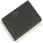
| 描述 | IC MCU USB EZ FX1 16KB 128LQFPUSB 接口集成电路 EZ USB FX1 LO Pwr Hi COM |
| 产品分类 | |
| I/O数 | 40 |
| 品牌 | Cypress Semiconductor Corp |
| 产品手册 | |
| 产品图片 |
|
| rohs | 符合RoHS无铅 / 符合限制有害物质指令(RoHS)规范要求 |
| 产品系列 | 接口 IC,USB 接口集成电路,Cypress Semiconductor CY7C64713-128AXCEZ-USB FX1™ |
| 数据手册 | |
| 产品型号 | CY7C64713-128AXC |
| PCN组件/产地 | http://www.cypress.com/?docID=47157http://www.cypress.com/?docID=48115http://www.cypress.com/?docID=49741 |
| RAM容量 | 16K x 8 |
| 产品种类 | USB 接口集成电路 |
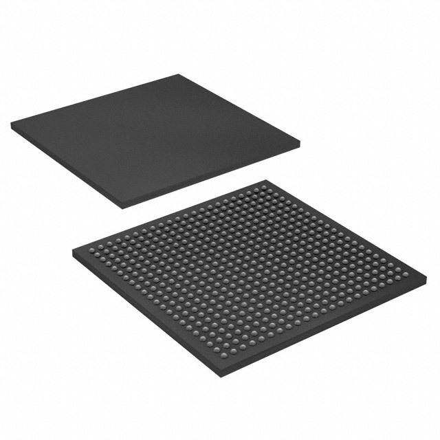
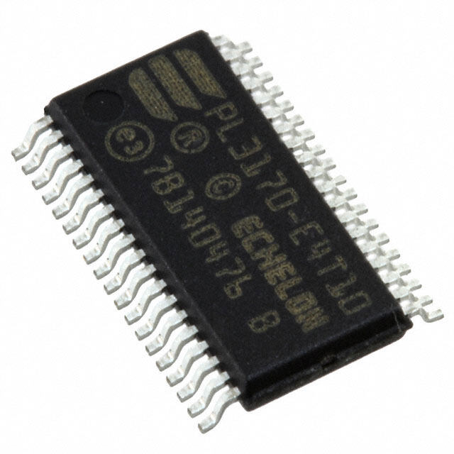
| 供应商器件封装 | 128-TQFP(14x20) |
| 其它名称 | 428-1678 |
| 包装 | 托盘 |
| 商标 | Cypress Semiconductor |
| 商标名 | EZ-USB |
| 安装类型 | 表面贴装 |
| 安装风格 | SMD/SMT |
| 封装 | Tray |
| 封装/外壳 | 128-LQFP |
| 封装/箱体 | TQFP-128 |
| 工作温度 | 0°C ~ 70°C |
| 工作电源电压 | 3.3 V |
| 工厂包装数量 | 136 |
| 应用 | USB 微控制器 |
| 接口 | I²C, USB, USART |
| 接口类型 | GPIF, I2C, USART |
| 控制器系列 | CY7C647xx |
| 数据速率 | 12 Mbps |
| 最大工作温度 | + 70 C |
| 最小工作温度 | 0 C |
| 标准 | USB 2.0 |
| 标准包装 | 72 |
| 核心处理器 | 8051 |
| 电压-电源 | 3.15 V ~ 3.45 V |
| 程序存储器类型 | ROMless |
| 类型 | Microcontroller |
| 系列 | CY7C64713 |
| 速度 | Full-Speed |
| 配用 | /product-detail/zh/CY3654-P03/428-1339-ND/464823 |


- 商务部:美国ITC正式对集成电路等产品启动337调查
- 曝三星4nm工艺存在良率问题 高通将骁龙8 Gen1或转产台积电
- 太阳诱电将投资9.5亿元在常州建新厂生产MLCC 预计2023年完工
- 英特尔发布欧洲新工厂建设计划 深化IDM 2.0 战略
- 台积电先进制程称霸业界 有大客户加持明年业绩稳了
- 达到5530亿美元!SIA预计今年全球半导体销售额将创下新高
- 英特尔拟将自动驾驶子公司Mobileye上市 估值或超500亿美元
- 三星加码芯片和SET,合并消费电子和移动部门,撤换高东真等 CEO
- 三星电子宣布重大人事变动 还合并消费电子和移动部门
- 海关总署:前11个月进口集成电路产品价值2.52万亿元 增长14.8%


PDF Datasheet 数据手册内容提取
CY7C64713 EZ-USB FX1™ USB Microcontroller Full Speed USB Peripheral Controller EZ-USB FX1™ USB Microcontroller Full Speed USB Peripheral Controller Features ❐Up to 48 MHz clock rate ❐Four clocks for each instruction cycle ■Single chip integrated USB transceiver, SIE, and enhanced 8051 microprocessor ❐Two USARTS ■Fit, form, and function upgradable to the FX2LP (CY7C68013A) ❐Three counters or timers ❐Pin compatible ❐Expanded interrupt system ❐Object code compatible ❐Two data pointers ❐Functionally compatible (FX1 functionality is a subset of the ■3.3 V operation with 5 V tolerant inputs FX2LP) ■Smart SIE ■Draws no more than 65 mA in any mode, making the FX1 ■Vectored USB interrupts suitable for bus powered applications ■Separate data buffers for the setup and DATA portions of a ■Software: 8051 runs from internal RAM, which is: CONTROL transfer ❐Downloaded using USB ■Integrated I2C controller, running at 100 or 400 KHz ❐Loaded from EEPROM ■48 MHz, 24 MHz, or 12 MHz 8051 operation ❐External memory device (128 pin configuration only) ■Four integrated FIFOs ■16 KB of on-chip code/data RAM ❐Brings glue and FIFOs inside for lower system cost ■Four programmable BULK/INTERRUPT/ISOCHRONOUS endpoints ❐Automatic conversion to and from 16-bit buses ❐Master or slave operation ❐Buffering options: double, triple, and quad ❐FIFOs can use externally supplied clock or asynchronous ■Additional programmable (BULK/INTERRUPT) 64-byte strobes endpoint ❐Easy interface to ASIC and DSP ICs ■8- or 16-bit external data interface ■Vectored for FIFO and GPIF Interrupts ■Smart media standard ECC generation ■Up to 40 general purpose IOs (GPIO) ■GPIF ■Four package options: ❐Allows direct connection to most parallel interfaces; 8- and 16-bit ❐128-pin TQFP ❐Programmable waveform descriptors and configuration ❐100-pin TQFP registers to define waveforms ❐56-pin SSOP ❐Supports multiple ready (RDY) inputs and Control (CTL) outputs ❐56-pin QFN Pb-free ■Integrated, industry standard 8051 with enhanced features: Errata: For information on silicon errata, see “Errata” on page71. Details include trigger conditions, devices affected, and proposed workaround. CypressSemiconductorCorporation • 198 Champion Court • SanJose, CA 95134-1709 • 408-943-2600 Document Number: 38-08039 Rev. *L Revised March 9, 2014
CY7C64713 Logic Block Diagram High performance micro 24 MHz using standard tools Ext. XTAL with lower-power options FX1 Address (16) Data (8) /0.5 I2C VC1C.5k xP2L0L //12..00 fo1u28r /0c25l4o1/c4 kC8s o/McreyHczle, a Bus (8) AdditionalM IOass t(e24r) incAlubduinndga tnwto I /UOSARTS connected for at enumeration D 6) / ADDR (9) proGgeranmermalable I/F DD+– XUCSVBR SCmYart 1R6A KMB Address (1 ECC GPIF RCDTLY ((66)) sAtotTa AAnPdSaII,Cr dE/sDP SsPu,P ce hotc ra. bsus Integrated USB full speed XCVR Engine Up to 96 MBytes 4 kB 8/16 burst rate FIFO Enhanced USB core ‘Soft Configuration’ FIFO and endpoint memory Simplifies 8051 code Easy firmware changes (master or slave operation) Document Number: 38-08039 Rev. *L Page 2 of 74
CY7C64713 Contents Functional Description .....................................................4 GPIF Synchronous Signals .......................................52 Applications ......................................................................4 Slave FIFO Synchronous Read .................................53 Functional Overview ........................................................4 Slave FIFO Asynchronous Read ...............................54 USB Signaling Speed ..................................................4 Slave FIFO Synchronous Write .................................55 8051 Microprocessor ...................................................4 Slave FIFO Asynchronous Write ...............................56 I2C Bus ........................................................................5 Slave FIFO Synchronous Packet End Strobe ...........56 Buses ..........................................................................5 Slave FIFO Asynchronous Packet End Strobe .........58 USB Boot Methods ......................................................5 Slave FIFO Output Enable ........................................58 ReNumeration™ ..........................................................6 Slave FIFO Address to Flags/Data ............................58 Bus-powered Applications ...........................................6 Slave FIFO Synchronous Address ............................59 Interrupt System ..........................................................6 Slave FIFO Asynchronous Address ..........................59 Reset and Wakeup ......................................................8 Sequence Diagram ....................................................60 Program/Data RAM .....................................................9 Ordering Information ......................................................64 Endpoint RAM ...........................................................11 Ordering Code Definitions .........................................64 External FIFO Interface .............................................11 Package Diagrams ..........................................................65 GPIF ..........................................................................12 Quad Flat Package No Leads (QFN) Package ECC Generation ........................................................13 Design Notes ...................................................................68 USB Uploads and Downloads ...................................13 Acronyms ........................................................................70 Autopointer Access ...................................................13 Document Conventions .................................................70 I2C Controller .............................................................13 Units of Measure .......................................................70 Compatible with Previous Generation Errata ...............................................................................71 EZ-USB FX2 .....................................................................14 Part Numbers Affected ..............................................71 Pin Assignments ............................................................14 EZ-USB FX1 Qualification Status ..............................71 CY7C64713 Pin Definitions ............................................20 EZ-USB FX1 Errata Summary ..................................71 Register Summary ..........................................................28 Document History Page .................................................72 Absolute Maximum Ratings ..........................................47 Sales, Solutions, and Legal Information ......................74 Operating Conditions .....................................................47 Worldwide Sales and Design Support .......................74 DC Characteristics .........................................................47 Products ....................................................................74 USB Transceiver .......................................................47 PSoC® Solutions ......................................................74 AC Electrical Characteristics ........................................48 Cypress Developer Community .................................74 USB Transceiver .......................................................48 Technical Support .....................................................74 PORTC Strobe Feature Timings ...............................51 Document Number: 38-08039 Rev. *L Page 3 of 74
CY7C64713 Functional Description FX1 does not support the low speed signaling mode of 1.5 Mbps or the high speed mode of 480 Mbps. EZ-USB FX1 (CY7C64713) is a full speed, highly integrated, USB microcontroller. By integrating the USB transceiver, Serial 8051 Microprocessor Interface Engine (SIE), enhanced 8051 microcontroller, and a The 8051 microprocessor embedded in the FX1 family has programmable peripheral interface in a single chip, Cypress has 256bytes of register RAM, an expanded interrupt system, three created a very cost effective solution that provides superior timer/counters, and two USARTs. time-to-market advantages. The EZ-USB FX1 is more economical, because it incorporates 8051 Clock Frequency the USB transceiver and provides a smaller footprint solution FX1 has an on-chip oscillator circuit that uses an external than the USB SIE or external transceiver implementations. With 24MHz (±100 ppm) crystal with the following characteristics: EZ-USB FX1, the Cypress Smart SIE handles most of the USB protocol in hardware, freeing the embedded microcontroller for ■Parallel resonant application specific functions and decreasing the development ■Fundamental mode time to ensure USB compatibility. The General Programmable Interface (GPIF) and Master/Slave ■500 W drive level Endpoint FIFO (8 or 16-bit data bus) provide an easy and ■12 pF (5% tolerance) load capacitors. glueless interface to popular interfaces such as ATA, UTOPIA, EPP, PCMCIA, and most DSP/processors. An on-chip PLL multiplies the 24 MHz oscillator up to 480 MHz, as required by the transceiver/PHY, and the internal counters Four Pb-free packages are defined for the family: 56-pin SSOP, divide it down for use as the 8051 clock. The default 8051 clock 56-pin QFN, 100-pin TQFP, and 128-pin TQFP. frequency is 12 MHz. The clock frequency of the 8051 is dynamically changed by the 8051 through the CPUCS register. Applications The CLKOUT pin, which is three-stated and inverted using the ■DSL modems internal control bits, outputs the 50% duty cycle 8051 clock at the selected 8051 clock frequency which is 48, 24, or 12 MHz. ■ATA interface USARTS ■Memory card readers FX1 contains two standard 8051 USARTs, addressed by Special ■Legacy conversion devices Function Register (SFR) bits. The USART interface pins are available on separate I/O pins, and are not multiplexed with port ■Home PNA pins. ■Wireless LAN UART0 and UART1 can operate using an internal clock at ■MP3 players 230KBaud with no more than 1% baud rate error. 230 KBaud operation is achieved by an internally derived clock source that ■Networking generates overflow pulses at the appropriate time. The internal The Reference Designs section of the cypress website provides clock adjusts for the 8051 clock rate (48, 24, 12 MHz) such that additional tools for typical USB applications. Each reference it always presents the correct frequency for 230-KBaud design comes complete with firmware source and object code, operation.[1] schematics, and documentation. Please visit Special Function Registers http://www.cypress.com for more information. Certain 8051 SFR addresses are populated to provide fast Functional Overview access to critical FX1 functions. These SFR additions are shown in Table 1 on page 5. Bold type indicates non-standard, USB Signaling Speed enhanced 8051 registers. The two SFR rows that end with ‘0’ and ‘8’ contain bit addressable registers. The four I/O ports A–D use FX1 operates at one of the three rates defined in the USB the SFR addresses used in the standard 8051 for ports 0–3, Specification Revision 2.0, dated April 27, 2000: which are not implemented in the FX1. Because of the faster and Full speed, with a signaling bit rate of 12 Mbps. more efficient SFR addressing, the FX1 I/O ports are not addressable in the external RAM space (using the MOVX instruction). Note 1. 115-KBaud operation is also possible by programming the 8051 SMOD0 or SMOD1 bits to a ‘1’ for UART0 and UART1, respectively. Document Number: 38-08039 Rev. *L Page 4 of 74
CY7C64713 Figure 1. Crystal Configuration C1 24 MHz C2 12 pF 12 pF 12-pF capacitor values assumes a trace capacitance of 3 pF per side on a four layer FR4 PCA 20 × PLL Table 1. Special Function Registers x 8x 9x Ax Bx Cx Dx Ex Fx 0 IOA IOB IOC IOD SCON1 PSW ACC B 1 SP EXIF INT2CLR IOE SBUF1 2 DPL0 MPAGE INT4CLR OEA 3 DPH0 OEB 4 DPL1 OEC 5 DPH1 OED 6 DPS OEE 7 PCON 8 TCON SCON0 IE IP T2CON EICON EIE EIP 9 TMOD SBUF0 A TL0 AUTOPTRH1 EP2468STAT EP01STAT RCAP2L B TL1 AUTOPTRL1 EP24FIFOFLGS GPIFTRIG RCAP2H C TH0 reserved EP68FIFOFLGS TL2 D TH1 AUTOPTRH2 GPIFSGLDATH TH2 E CKCON AUTOPTRL2 GPIFSGLDATLX F reserved AUTOPTRSETUP GPIFSGLDATLNOX I2C Bus in place of the internally stored values (0xC0). Alternatively, it FX1 supports the I2C bus as a master only at 100/400 KHz. SCL boot-loads the EEPROM contents into an internal RAM (0xC2). If no EEPROM is detected, FX1 enumerates using internally and SDA pins have open drain outputs and hysteresis inputs. These signals must be pulled up to 3.3 V, even if no I2C device stored descriptors. The default ID values for FX1 are VID/PID/DID (0x04B4, 0x6473, 0xAxxx where xxx=Chip is connected. revision).[2] Buses Table 2. Default ID Values for FX1 All packages: 8 or 16-bit ‘FIFO’ bidirectional data bus, Default VID/PID/DID multiplexed on I/O ports B and D. 128-pin package: adds 16-bit output only 8051 address bus, 8-bit bidirectional data bus. Vendor ID 0x04B4 Cypress Semiconductor USB Boot Methods Product ID 0x6473 EZ-USB FX1 During the power up sequence, internal logic checks the I2C port Device 0xAnnn Depends on chip revision (nnn = chip for the connection of an EEPROM whose first byte is either 0xC0 release revision where first silicon = 001) or 0xC2. If found, it uses the VID/PID/DID values in the EEPROM Notes 2. The I2C bus SCL and SDA pins must be pulled up, even if an EEPROM is not connected. Otherwise this detection method does not work properly. Document Number: 38-08039 Rev. *L Page 5 of 74
CY7C64713 ReNumeration™ USB-Interrupt Autovectors Because the FX1’s configuration is soft, one chip can take on the The main USB interrupt is shared by 27 interrupt sources. The identities of multiple distinct USB devices. FX1 provides a second level of interrupt vectoring, called Autovectoring, to save code and processing time that is normally When first plugged into the USB, the FX1 enumerates required to identify the individual USB interrupt source. When a automatically and downloads firmware and the USB descriptor USB interrupt is asserted, the FX1 pushes the program counter tables over the USB cable. Next, the FX1 enumerates again, this on to its stack and then jumps to address 0x0043, where it time as a device defined by the downloaded information. This expects to find a “jump” instruction to the USB Interrupt service patented two step process, called ReNumeration, happens routine. instantly when the device is plugged in, with no indication that the initial download step has occurred. The FX1 jump instruction is encoded as shown in Table3. Two control bits in the USBCS (USB Control and Status) register If Autovectoring is enabled (AV2EN = 1 in the INTSETUP control the ReNumeration process: DISCON and RENUM. To register), the FX1 substitutes its INT2VEC byte. Therefore, if the simulate a USB disconnect, the firmware sets DISCON to 1. To high byte (“page”) of a jump table address is preloaded at reconnect, the firmware clears DISCON to 0. location 0x0044, the automatically inserted INT2VEC byte at 0x0045 directs the jump to the correct address out of the 27 Before reconnecting, the firmware sets or clears the RENUM bit addresses within the page. to indicate if the firmware or the Default USB Device handles device requests over endpoint zero: FIFO/GPIF Interrupt (INT4) Just as the USB Interrupt is shared among 27 individual ■RENUM = 0, the Default USB Device handles device requests USB-interrupt sources, the FIFO/GPIF interrupt is shared among ■RENUM = 1, the firmware handles device requests 14 individual FIFO/GPIF sources. The FIFO/GPIF Interrupt, such as the USB Interrupt, can employ autovectoring. Table 4 on page Bus-powered Applications 7 shows the priority and INT4VEC values for the 14 FIFO/GPIF The FX1 fully supports bus powered designs by enumerating interrupt sources. with less than 100 mA as required by the USB specification. FIFO/GPIF Interrupt (INT4) Interrupt System Just as the USB Interrupt is shared among 27 individual USB-interrupt sources, the FIFO/GPIF interrupt is shared among INT2 Interrupt Request and Enable Registers 14 individual FIFO/GPIF sources. The FIFO/GPIF Interrupt, such FX1 implements an autovector feature for INT2 and INT4. There as the USB Interrupt, can employ autovectoring. are 27 INT2 (USB) vectors, and 14 INT4 (FIFO/GPIF) vectors. Table 4 on page 7 shows the priority and INT4VEC values for the See EZ-USB Technical Reference Manual (TRM) for more 14 FIFO/GPIF interrupt sources. details. Table 3. INT2 USB Interrupts USB INTERRUPT TABLE FOR INT2 Priority INT2VEC Value Source Notes 1 00 SUDAV Setup Data Available 2 04 SOF Start of Frame 3 08 SUTOK Setup Token Received 4 0C SUSPEND USB Suspend request 5 10 USB RESET Bus reset 6 14 Reserved 7 18 EP0ACK FX1 ACK’d the CONTROL Handshake 8 1C Reserved 9 20 EP0-IN EP0-IN ready to be loaded with data 10 24 EP0-OUT EP0-OUT has USB data 11 28 EP1-IN EP1-IN ready to be loaded with data 12 2C EP1-OUT EP1-OUT has USB data 13 30 EP2 IN: buffer available. OUT: buffer has data 14 34 EP4 IN: buffer available. OUT: buffer has data 15 38 EP6 IN: buffer available. OUT: buffer has data 16 3C EP8 IN: buffer available. OUT: buffer has data 17 40 IBN IN-Bulk-NAK (any IN endpoint) Document Number: 38-08039 Rev. *L Page 6 of 74
CY7C64713 Table 3. INT2 USB Interrupts (continued) USB INTERRUPT TABLE FOR INT2 Priority INT2VEC Value Source Notes 18 44 Reserved 19 48 EP0PING EP0 OUT was Pinged and it NAK’d 20 4C EP1PING EP1 OUT was Pinged and it NAK’d 21 50 EP2PING EP2 OUT was Pinged and it NAK’d 22 54 EP4PING EP4 OUT was Pinged and it NAK’d 23 58 EP6PING EP6 OUT was Pinged and it NAK’d 24 5C EP8PING EP8 OUT was Pinged and it NAK’d 25 60 ERRLIMIT Bus errors exceeded the programmed limit 26 64 27 68 Reserved 28 6C Reserved 29 70 EP2ISOERR ISO EP2 OUT PID sequence error 30 74 EP4ISOERR ISO EP4 OUT PID sequence error 31 78 EP6ISOERR ISO EP6 OUT PID sequence error 32 7C EP8ISOERR ISO EP8 OUT PID sequence error Table 4. Individual FIFO/GPIF Interrupt Sources Priority INT4VEC Value Source Notes 1 80 EP2PF Endpoint 2 Programmable Flag 2 84 EP4PF Endpoint 4 Programmable Flag 3 88 EP6PF Endpoint 6 Programmable Flag 4 8C EP8PF Endpoint 8 Programmable Flag 5 90 EP2EF Endpoint 2 Empty Flag [3] 6 94 EP4EF Endpoint 4 Empty Flag 7 98 EP6EF Endpoint 6 Empty Flag 8 9C EP8EF Endpoint 8 Empty Flag 9 A0 EP2FF Endpoint 2 Full Flag 10 A4 EP4FF Endpoint 4 Full Flag 11 A8 EP6FF Endpoint 6 Full Flag 12 AC EP8FF Endpoint 8 Full Flag 13 B0 GPIFDONE GPIF Operation Complete 14 B4 GPIFWF GPIF Waveform If Autovectoring is enabled (AV4EN = 1 in the INTSETUP pushes the program counter onto its stack and then jumps to register), the FX1 substitutes its INT4VEC byte. Therefore, if the address 0x0053, where it expects to find a “jump” instruction to high byte (“page”) of a jump-table address is preloaded at the ISR Interrupt service routine. location 0x0054, the automatically inserted INT4VEC byte at 0x0055 directs the jump to the correct address out of the 14 addresses within the page. When the ISR occurs, the FX1 Note 3. Errata: In Slave FIFO Asynchronous Word Wide mode, if a single word data is transferred from the USB host to EP2, configured as OUT Endpoint (EP) in the first transaction, then the Empty flag behaves incorrectly. This does not happen if the data size is more than one word in the first transaction. For more information, see the “Errata” on page71. Document Number: 38-08039 Rev. *L Page 7 of 74
CY7C64713 Reset and Wakeup during operation. A power on reset is defined as the time a reset is asserted when power is being applied to the circuit. A powered Reset Pin reset is defined to be when the FX1 has been previously powered on and operating and the RESET# pin is asserted. The input pin, RESET#, resets the FX1 when asserted. This pin has hysteresis and is active LOW. When a crystal is used with Cypress provides an application note which describes and the CY7C64713, the reset period must allow for the stabilization recommends power on reset implementation and is found on the of the crystal and the PLL. This reset period must be Cypress web site. While the application note discusses the FX2, approximately 5 ms after VCC has reached 3.0 Volts. If the the information provided applies also to the FX1. For more crystal input pin is driven by a clock signal the internal PLL information on reset implementation for the FX2 family of stabilizes in 200 s after VCC has reached 3.0 V[4]. Figure 2 on products visit http://www.cypress.com. page 8 shows a power on reset condition and a reset applied Figure 2. Reset Timing Plots RESET# RESET# VIL VIL 3.3 V 3.3 V 3.0 V VCC VCC 0 V 0 V T T RESET RESET Power on Reset Powered Reset wakeup interrupt. This applies irrespective of whether the FX1 is T able 5. Reset Timing Values connected to the USB or not. The FX1 exits the power down (USB suspend) state using one Condition T RESET of the following methods: Power On Reset with crystal 5 ms ■USB bus activity (if D+/D– lines are left floating, noise on these Power On Reset with external 200 s + Clock stability time lines may indicate activity to the FX1 and initiate a wakeup). clock ■External logic asserts the WAKEUP pin. Powered Reset 200 s ■External logic asserts the PA3/WU2 pin. Wakeup Pins The second wakeup pin, WU2, can also be configured as a The 8051 puts itself and the rest of the chip into a power down general purpose I/O pin. This allows a simple external R-C mode by setting PCON.0 = 1. This stops the oscillator and PLL. network to be used as a periodic wakeup source. Note that When WAKEUP is asserted by external logic, the oscillator WAKEUP is by default active LOW. restarts, after the PLL stabilizes, and then the 8051 receives a Note 4. If the external clock is powered at the same time as the CY7C64713 and has a stabilization wait period. It must be added to the 200 s. Document Number: 38-08039 Rev. *L Page 8 of 74
CY7C64713 Program/Data RAM external RAM or ROM is added, the external read and write strobes are suppressed for memory spaces that exist inside the Size chip. This allows the user to connect a 64 KByte memory without requiring the address decodes to keep clear of internal memory The FX1 has 16 KBytes of internal program/data RAM, where spaces. PSEN#/RD# signals are internally ORed to allow the 8051 to access it as both program and data memory. No USB control Only the internal 16 KBytes and scratch pad 0.5 KBytes RAM registers appear in this space. spaces have the following access: Two memory maps are shown in the following diagrams: ■USB download ■Figure 3 on page 9 Internal Code Memory, EA = 0 ■USB upload ■Figure 4 on page 10 External Code Memory, EA = 1. ■Setup data pointer Internal Code Memory, EA = 0 ■I2C interface boot load This mode implements the internal 16 KByte block of RAM (starting at 0) as combined code and data memory. When the Figure 3. Internal Code Memory, EA = 0. Inside FX1 Outside FX1 FFFF 7.5 KBytes USB regs and (OK to populate 4K FIFO buffers data memory (RD#,WR#) here—RD#/WR# E200 strobes are not E1FF active) 0.5 KBytes RAM E000 Data (RD#,WR#)* 48 KBytes External 40 KBytes Code External Memory Data (PSEN#) Memory (RD#,WR#) 3FFF (Ok to populate (OK to populate 16 KBytes RAM data memory program Code and Data here—RD#/WR# memory here— (PSEN#,RD#,WR#)* strobes are not PSEN# strobe active) is not active) 0000 Data Code *SUDPTR, USB upload/download, I2C interface boot access Document Number: 38-08039 Rev. *L Page 9 of 74
CY7C64713 External Code Memory, EA = 1 The bottom 16 KBytes of program memory is external, and therefore the bottom 16 KBytes of internal RAM is accessible only as data memory. Figure 4. External Code Memory, EA = 1 Inside FX1 Outside FX1 FFFF 7.5 KBytes USB regs and (OK to populate 4K FIFO buffers data memory (RD#,WR#) here—RD#/WR# E200 strobes are not E1FF 0.5 KBytes RAM active) E000 Data (RD#,WR#)* 40 KBytes External Data 64 KBytes Memory External (RD#,WR#) Code Memory (PSEN#) 3FFF (Ok to populate 16 KBytes data memory RAM here—RD#/WR# Data strobes are not (RD#,WR#)* active) 0000 Data Code *SUDPTR, USB upload/download, I2C interface boot access Document Number: 38-08039 Rev. *L Page 10 of 74
CY7C64713 Figure 5. Register Addresses FFFF 4 KBytes EP2-EP8 buffers (8 x 512) Not all Space is available for all transfer types F000 EFFF 2 KBytes RESERVED E800 E7FF 64 Bytes EP1IN E7C0 E7BF 64 Bytes EP1OUT E780 E77F 64 Bytes EP0 IN/OUT E740 E73F 64 Bytes RESERVED E700 E6FF 8051 Addressable Registers (512) E500 E4FF Reserved (128) E480 E47F 128 bytes GPIF Waveforms E400 E3FF Reserved (512) E200 E1FF 512 bytes 8051 xdata RAM E000 Endpoint RAM Table 6. Default Alternate Settings Size Alternate 0 1 2 3 Setting ■3 × 64 bytes (Endpoints 0 and 1) ep0 64 64 64 64 ■8 × 512 bytes (Endpoints 2, 4, 6, 8) ep1out 0 64 bulk 64 int 64 int Organization ep1in 0 64 bulk 64 int 64 int ■EP0—Bidirectional endpoint zero, 64 byte buffer ep2 0 64 bulk out (2×)64 int out (2×) 64 iso out (2×) ■EP1IN, EP1OUT—64 byte buffers, bulk or interrupt ep4 0 64 bulk out (2×)64 bulk out (2×)64 bulk out (2×) ■EP2, 4, 6, 8—Eight 512-byte buffers, bulk, interrupt, or ep6 0 64 bulk in (2×) 64 int in (2×) 64 iso in (2×) isochronous, of which only the transfer size is available. EP4 ep8 0 64 bulk in (2×) 64 bulk in (2×) 64 bulk in (2×) and EP8 are double buffered, while EP2 and 6 are either double, triple, or quad buffered. Regardless of the physical size External FIFO Interface of the buffer, each endpoint buffer accommodates only one full speed packet. For bulk endpoints, the maximum number of Architecture bytes it can accommodate is 64, even though the physical buffer size is 512 or 1024. For an ISOCHRONOUS endpoint The FX1 slave FIFO architecture has eight 512-byte blocks in the the maximum number of bytes it can accommodate is 1023. endpoint RAM that directly serve as FIFO memories, and are For endpoint configuration options, see Figure 6 on page 12. controlled by FIFO control signals (such as IFCLK, SLCS#, SLRD, SLWR, SLOE, PKTEND, and flags). The usable size of Setup Data Buffer these buffers depend on the USB transfer mode as described in the section Organization. A separate 8-byte buffer at 0xE6B8-0xE6BF holds the Setup data from a CONTROL transfer. In operation, some of the eight RAM blocks fill or empty from the SIE, while the others are connected to the I/O transfer logic. The Default Alternate Settings transfer logic takes two forms: the GPIF for internally generated In the following table, ‘0’ means “not implemented”, and ‘2×’ control signals or the slave FIFO interface for externally means “double buffered”. controlled transfers. Document Number: 38-08039 Rev. *L Page 11 of 74
CY7C64713 Figure 6. Endpoint Configuration EP0 IN&OUT 64 64 64 64 64 64 64 64 64 64 64 64 EP1 IN 64 64 64 64 64 64 64 64 64 64 64 64 EP1 OUT 64 64 64 64 64 64 64 64 64 64 64 64 EP2 EP2 EP2 EP2 EP2 EP2 EP2 EP2 EP2 EP2 EP2 EP2 64 64 64 64 64 64 64 1023 1023 1023 64 64 64 64 64 64 64 1023 1023 EP4 EP4 EP4 64 64 64 64 64 64 64 1023 1023 1023 EP6 1023 1023 64 64 64 64 64 64 64 EP6 EP6 EP6 EP6 EP6 EP6 EP6 EP6 EP6 64 1023 64 64 64 64 64 64 1023 1023 1023 1023 1023 64 64 64 64 64 64 64 EP8 EP8 EP8 EP8 EP8 64 64 1023 64 64 1023 64 64 1023 64 64 1023 64 64 64 64 64 64 64 64 1 2 3 4 5 6 7 8 9 10 11 12 Master/Slave Control Signals as strobes, rather than a clock qualifier as in the synchronous mode. The signals SLRD, SLWR, SLOE, and PKTEND are gated The FX1 endpoint FIFOS are implemented as eight physically by the signal SLCS#. distinct 256 × 16 RAM blocks. The 8051/SIE can switch any of the RAM blocks between two domains: the USB (SIE) domain GPIF and FIFO Clock Rates and the 8051-I/O Unit domain. This switching is done instantaneously, giving essentially zero transfer time between An 8051 register bit selects one of two frequencies for the “USB FIFOS” and “Slave FIFOS”. While they are physically the internally supplied interface clock: 30 MHz and 48 MHz. same memory, no bytes are actually transferred between Alternatively, an externally supplied clock of 5 to 48 MHz feeding buffers. the IFCLK pin is used as the interface clock. IFCLK is configured to function as an output clock when the GPIF and FIFOs are At any time, some RAM blocks fill or empty with USB data under internally clocked. An output enable bit in the IFCONFIG register SIE control, while other RAM blocks are available to the 8051 turns this clock output off, if desired. Another bit within the and the I/O control unit. The RAM blocks operate as a single-port IFCONFIG register inverts the IFCLK signal whether internally or in the USB domain, and dual port in the 8051-I/O domain. The externally sourced. blocks are configured as single, double, triple, or quad buffered. The I/O control unit implements either an internal master (M for GPIF master) or external master (S for Slave) interface. The GPIF is a flexible 8 or 16-bit parallel interface driven by a In Master (M) mode, the GPIF internally controls FIFOADR[1..0] user programmable finite state machine. It allows the to select a FIFO. The RDY pins (two in the 56-pin package, six CY7C64713 to perform local bus mastering, and can implement in the 100-pin and 128-pin packages) are used as flag inputs a wide variety of protocols such as ATA interface, printer parallel from an external FIFO or other logic if desired. The GPIF is run port, and Utopia. from either an internally derived clock or an externally supplied The GPIF has six programmable control outputs (CTL), nine clock (IFCLK), at a rate that transfers data up to 96 Megabytes/s address outputs (GPIFADRx), and six general purpose Ready (48 MHz IFCLK with 16-bit interface). inputs (RDY). The data bus width is 8 or 16 bits. Each GPIF In Slave (S) mode, the FX1 accepts either an internally derived vector defines the state of the control outputs, and determines clock or an externally supplied clock (IFCLK with a maximum what state a Ready input (or multiple inputs) must be before frequency of 48 MHz) and SLCS#, SLRD, SLWR, SLOE, proceeding. The GPIF vector is programmed to advance a FIFO PKTEND signals from external logic. When using an external to the next data value, advance an address, and so on. A IFCLK, the external clock must be present before switching to sequence of the GPIF vectors create a single waveform that the external clock with the IFCLKSRC bit. Each endpoint can executes to perform the data move between the FX1 and the individually be selected for byte or word operation by an internal external device. configuration bit, and a Slave FIFO Output Enable signal SLOE enables data of the selected width. External logic must ensure Six Control OUT Signals that the output enable signal is inactive when writing data to a The 100-pin and 128-pin packages bring out all six Control slave FIFO. The slave interface can also operate Output pins (CTL0–CTL5). The 8051 programs the GPIF unit to asynchronously, where the SLRD and SLWR signals act directly define the CTL waveforms. The 56-pin package brings out three Document Number: 38-08039 Rev. *L Page 12 of 74
CY7C64713 of these signals: CTL0–CTL2. CTLx waveform edges are Write any value to ECCRESET, then pass data across the GPIF programmed to make transitions as fast as once per clock or Slave FIFO interface. The ECC for the first 512 bytes of data (20.8ns using a 48 MHz clock). is calculated and stored in ECC1; ECC2 is not used. After the ECC is calculated, the value in ECC1 does not change until the Six Ready IN Signals ECCRESET is written again, even if more data is subsequently The 100-pin and 128-pin packages bring out all six Ready inputs passed across the interface (RDY0–RDY5). The 8051 programs the GPIF unit to test the USB Uploads and Downloads RDY pins for GPIF branching. The 56 pin package brings out two of these signals, RDY0–1. The core has the ability to directly edit the data contents of the internal 16 KByte RAM and of the internal 512 byte scratch pad Nine GPIF Address OUT Signals RAM via a vendor specific command. This capability is normally Nine GPIF address lines are available in the 100-pin and 128-pin used when ‘soft’ downloading user code and is available only to packages: GPIFADR[8..0]. The GPIF address lines allow and from the internal RAM, only when the 8051 is held in reset. indexing through up to a 512 byte block of RAM. If more address The available RAM spaces are 16 KBytes from 0x0000–0x3FFF lines are needed, I/O port pins are used. (code/data) and 512 bytes from 0xE000–0xE1FF (scratch pad data RAM).[5] Long Transfer Mode Autopointer Access In Master mode, the 8051 appropriately sets the GPIF transaction count registers (GPIFTCB3, GPIFTCB2, GPIFTCB1, FX1 provides two identical autopointers. They are similar to the or GPIFTCB0) for unattended transfers of up to 232 transactions. internal 8051 data pointers, but with an additional feature: they The GPIF automatically throttles data flow to prevent under or can optionally increment after every memory access. This overflow until the full number of requested transactions are capability is available to and from both internal and external complete. The GPIF decrements the value in these registers to RAM. The autopointers are available in external FX1 registers, represent the current status of the transaction. under the control of a mode bit (AUTOPTRSETUP.0). Using the external FX1 autopointer access (at 0xE67B–0xE67C) allows ECC Generation the autopointer to access all RAM, internal and external, to the part. Also, the autopointers can point to any FX1 register or The EZ-USB FX1 can calculate ECCs (Error Correcting Codes) endpoint buffer space. When autopointer access to external on data that pass across its GPIF or Slave FIFO interfaces. There are two ECC configurations: Two ECCs, each calculated memory is enabled, the location 0xE67B and 0xE67C in XDATA and the code space cannot be used. over 256 bytes (SmartMedia™ Standard); and one ECC calculated over 512 bytes. I2C Controller The ECC can correct any one-bit error or detect any two-bit error. FX1 has one I2C port that is driven by two internal controllers: Note To use the ECC logic, the GPIF or Slave FIFO interface one that automatically operates at boot time to load VID/PID/DID must be configured for byte-wide operation. and configuration information; and another that the 8051, once running, uses to control external I2C devices. The I2C port ECC Implementation operates in master mode only. The two ECC configurations are selected by the ECCM bit: I2C Port Pins 0.0.0.1 ECCM = 0 The I2C pins SCL and SDA must have external 2.2 k pull up Two 3-byte ECCs, each calculated over a 256-byte block of data. resistors even if no EEPROM is connected to the FX1. External This configuration conforms to the SmartMedia Standard. EEPROM device address pins must be configured properly. See Table7 for configuring the device address pins. Write any value to ECCRESET, then pass data across the GPIF or Slave FIFO interface. The ECC for the first 256 bytes of data Table 7. Strap Boot EEPROM Address Lines to These Values is calculated and stored in ECC1. The ECC for the next 256 bytes is stored in ECC2. After the second ECC is calculated, the values Bytes Example EEPROM A2 A1 A0 in the ECCx registers do not change until the ECCRESET is 16 24LC00[6] N/A N/A N/A written again, even if more data is subsequently passed across 128 24LC01 0 0 0 the interface. 256 24LC02 0 0 0 0.0.0.2 ECCM = 1 4K 24LC32 0 0 1 One 3-byte ECC calculated over a 512-byte block of data. 8K 24LC64 0 0 1 16K 24LC128 0 0 1 Notes 5. After the data is downloaded from the host, a ‘loader’ executes from the internal RAM to transfer downloaded data to the external memory. 6. This EEPROM has no address pins. Document Number: 38-08039 Rev. *L Page 13 of 74
CY7C64713 I2C Interface Boot Load Access plus a combination diagram showing which of the full set of At power on reset the I2C interface boot loader loads the signals are available in the 128, 100, and 56-pin packages. VID/PID/DID configuration bytes and up to 16 KBytes of The signals on the left edge of the 56-pin package in Figure 7 on program/data. The available RAM spaces are 16 KBytes from page 15 are common to all versions in the FX1 family. Three 0x0000–0x3FFF and 512 bytes from 0xE000–0xE1FF. The 8051 modes are available in all package versions: Port, GPIF master, is in reset. I2C interface boot loads only occur after power on and Slave FIFO. These modes define the signals on the right reset. edge of the diagram. The 8051 selects the interface mode using the IFCONFIG[1:0] register bits. Port mode is the power on I2C Interface General Purpose Access default configuration. The 8051 can control peripherals connected to the I2C bus using The 100-pin package adds functionality to the 56-pin package by the I2CTL and I2DAT registers. FX1 provides I2C master control adding these pins: only, because it is never an I2C slave. ■PORTC or alternate GPIFADR[7:0] address signals Compatible with Previous Generation EZ-USB FX2 ■PORTE or alternate GPIFADR[8] address signal and seven The EZ-USB FX1 is fit, form, and function upgradable to the additional 8051 signals EZ-USB FX2LP. This makes for an easy transition for designers wanting to upgrade their systems from full speed to high speed ■Three GPIF Control signals designs. The pinout and package selection are identical, and all ■Four GPIF Ready signals firmware developed for the FX1 function in the FX2LP with proper addition of high speed descriptors and speed switching ■Nine 8051 signals (two USARTs, three timer inputs, INT4,and code. INT5#) Pin Assignments ■BKPT, RD#, WR#. The 128-pin package adds the 8051 address and data buses Figure 7 on page 15 identifies all signals for the three package plus control signals. Note that two of the required signals, RD# types. The following pages illustrate the individual pin diagrams, and WR#, are present in the 100-pin version. In the 100-pin and 128-pin versions, an 8051 control bit is set to pulse the RD# and WR# pins when the 8051 reads from and writes to the PORTC. Document Number: 38-08039 Rev. *L Page 14 of 74
CY7C64713 Figure 7. Signals Port GPIF Master Slave FIFO PD7 FD[15] FD[15] PD6 FD[14] FD[14] PD5 FD[13] FD[13] PD4 FD[12] FD[12] PD3 FD[11] FD[11] PD2 FD[10] FD[10] PD1 FD[9] FD[9] PD0 FD[8] FD[8] PB7 FD[7] FD[7] PB6 FD[6] FD[6] PB5 FD[5] FD[5] XTALIN PB4 FD[4] FD[4] XTALOUT PB3 FD[3] FD[3] RESET# PB2 FD[2] FD[2] WAKEUP# PB1 FD[1] FD[1] SCL 56 PB0 FD[0] FD[0] SDA RDY0 SLRD RDY1 SLWR CTL0 FLAGA CTL1 FLAGB CTL2 FLAGC INT0#/PA0 INT0#/PA0 INT0#/ PA0 IFCLK INT1#/PA1 INT1#/PA1 INT1#/ PA1 CLKOUT PA2 PA2 SLOE WU2/PA3 WU2/PA3 WU2/PA3 DPLUS PA4 PA4 FIFOADR0 DMINUS PA5 PA5 FIFOADR1 PA6 PA6 PKTEND PA7 PA7 PA7/FLAGD/SLCS# CTL3 CTL4 CTL5 RDY2 RDY3 100 RDY4 RDY5 BKPT PORTC7/GPIFADR7 PORTC6/GPIFADR6 PORTC5/GPIFADR5 PORTC4/GPIFADR4 RxD0 PORTC3/GPIFADR3 TxD0 PORTC2/GPIFADR2 RxD1 PORTC1/GPIFADR1 TxD1 PORTC0/GPIFADR0 INT4 INT5# PE7/GPIFADR8 PE6/T2EX T2 PE5/INT6 T1 PE4/RxD1OUT T0 PE3/RxD0OUT PE2/T2OUT PE1/T1OUT RD# PE0/T0OUT WR# D7 CS# D6 OE# D5 PSEN# D4 D3 A15 D2 A14 D1 A13 D0 A12 A11 A10 128 A9 A8 A7 A6 A5 A4 EA A3 A2 A1 A0 Document Number: 38-08039 Rev. *L Page 15 of 74
CY7C64713 Figure 8. CY7C64713 128-pin TQFP Pin Assignment 1 1 1 1 1 1 1 1 1 1 1 1 1 1 1 1 1 1 1 1 1 1 1 1 1 1 2 2 2 2 2 2 2 2 2 1 1 1 1 1 1 1 1 1 1 0 0 0 0 0 0 0 8 7 6 5 4 3 2 1 0 9 8 7 6 5 4 3 2 1 0 9 8 7 6 5 4 3 A A A G P P P P A A A A G P P P P P P P P V IN P P P 10 9 8 ND D7/F D6/F D5/F D4/F 7 6 5 4 ND E7/G E6/T E5/IN E4/R E3/R E2/T E1/T E0/T CC T5# D3/F D2/F D1/F 1 CLKOUT D15 D14 D13 D12 PIFA 2EX T6 XD1 XD0 2OU 1OU 0OU D11 D10 D9 PD0/FD8 102 2 VCC D O O T T T *WAKEUP 101 3 GND R8 UT UT VCC 100 4 RDY0/*SLRD RESET# 99 5 RDY1/*SLWR CTL5 98 6 RDY2 A3 97 7 RDY3 A2 96 8 RDY4 A1 95 9 RDY5 A0 94 10 AVCC GND 93 11 XTALOUT PA7/*FLAGD/SLCS# 92 12 XTALIN PA6/*PKTEND 91 13 AGND PA5/FIFOADR1 90 14 NC PA4/FIFOADR0 89 15 NC D7 88 16 NC D6 87 17 AVCC D5 86 18 DPLUS CY7C64713 PA3/*WU2 85 19 DMINUS 128-pin TQFP PA2/*SLOE 84 20 AGND PA1/INT1# 83 21 A11 PA0/INT0# 82 22 A12 VCC 81 23 A13 GND 80 24 A14 PC7/GPIFADR7 79 25 A15 PC6/GPIFADR6 78 26 VCC PC5/GPIFADR5 77 27 GND PC4/GPIFADR4 76 28 INT4 PC3/GPIFADR3 75 29 T0 PC2/GPIFADR2 74 30 T1 PC1/GPIFADR1 73 31 T2 PC0/GPIFADR0 72 32 *IFCLK CTL2/*FLAGC 71 33 RESERVED CTL1/*FLAGB 70 34 BKPT CTL0/*FLAGA 69 35 EA VCC 68 36 SCL CTL4 67 37 SDA CTL3 66 38 OE# GND 65 P P P P P P P P P B B B B B B B B S 0 1 2 3 T R T R 4 5 6 7 E R W C V /F /F /F /F V G X X X X /F /F /F /F G V N D R S C D D D D C N D D D D D D D D N D D D D D C # # # # C 0 1 2 3 C D 0 0 1 1 4 5 6 7 D 0 1 2 3 4 C 3 4 4 4 4 4 4 4 4 4 4 5 5 5 5 5 5 5 5 5 5 6 6 6 6 6 9 0 1 2 3 4 5 6 7 8 9 0 1 2 3 4 5 6 7 8 9 0 1 2 3 4 * indicates programmable polarity Document Number: 38-08039 Rev. *L Page 16 of 74
CY7C64713 Figure 9. CY7C64713 100-pin TQFP Pin Assignment 1 9 9 9 9 9 9 9 9 9 9 8 8 8 8 8 8 8 8 8 0 9 8 7 6 5 4 3 2 1 0 9 8 7 6 5 4 3 2 1 0 C G P P P P G P P P P P P P P V IN P P P LKOUT ND D7/FD15 D6/FD14 D5/FD13 D4/FD12 ND E7/GPIFA E6/T2EX E5/INT6 E4/RXD1 E3/RXD0 E2/T2OU E1/T1OU E0/T0OU CC T5# D3/FD11 D2/FD10 D1/FD9 O O T T T D R U U 8 T T 1 VCC PD0/FD8 80 2 GND *WAKEUP 79 3 RDY0/*SLRD VCC 78 4 RDY1/*SLWR RESET# 77 5 RDY2 CTL5 76 6 RDY3 GND 75 7 RDY4 PA7/*FLAGD/SLCS# 74 8 RDY5 PA6/*PKTEND 73 9 AVCC PA5/FIFOADR1 72 10 XTALOUT PA4/FIFOADR0 71 11 XTALIN PA3/*WU2 70 12 AGND PA2/*SLOE 69 13 NC PA1/INT1# 68 14 NC PA0/INT0# 67 15 NC CY7C64713 VCC 66 100-pin TQFP 16 AVCC GND 65 17 DPLUS PC7/GPIFADR7 64 18 DMINUS PC6/GPIFADR6 63 19 AGND PC5/GPIFADR5 62 20 VCC PC4/GPIFADR4 61 21 GND PC3/GPIFADR3 60 22 INT4 PC2/GPIFADR2 59 23 T0 PC1/GPIFADR1 58 24 T1 PC0/GPIFADR0 57 25 T2 CTL2/*FLAGC 56 26 *IFCLK CTL1/*FLAGB 55 27 RESERVED CTL0/*FLAGA 54 28 BKPT VCC 53 29 SCL CTL4 52 30 SDA CTL3 51 P P P P P P P P B B B B B B B B 0 1 2 3 T R T R 4 5 6 7 R W V /F /F /F /F V G X X X X /F /F /F /F G V G D R C D D D D C N D D D D D D D D N C N # # C 0 1 2 3 C D 0 0 1 1 4 5 6 7 D C D 3 3 3 3 3 3 3 3 3 4 4 4 4 4 4 4 4 4 4 5 1 2 3 4 5 6 7 8 9 0 1 2 3 4 5 6 7 8 9 0 * indicates programmable polarity Document Number: 38-08039 Rev. *L Page 17 of 74
CY7C64713 Figure 10. CY7C64713 56-pin SSOP Pin Assignment CY7C64713 56-pin SSOP 1 PD5/FD13 PD4/FD12 56 2 PD6/FD14 PD3/FD11 55 3 PD7/FD15 PD2/FD10 54 4 GND PD1/FD9 53 5 CLKOUT PD0/FD8 52 6 VCC *WAKEUP 51 7 GND VCC 50 8 RDY0/*SLRD RESET# 49 9 RDY1/*SLWR GND 48 10 AVCC PA7/*FLAGD/SLCS# 47 11 XTALOUT PA6/PKTEND 46 12 XTALIN PA5/FIFOADR1 45 13 AGND PA4/FIFOADR0 44 14 AVCC PA3/*WU2 43 15 DPLUS PA2/*SLOE 42 16 DMINUS PA1/INT1# 41 17 AGND PA0/INT0# 40 18 VCC VCC 39 19 GND CTL2/*FLAGC 38 20 *IFCLK CTL1/*FLAGB 37 21 RESERVED CTL0/*FLAGA 36 22 SCL GND 35 23 SDA VCC 34 24 VCC GND 33 25 PB0/FD0 PB7/FD7 32 26 PB1/FD1 PB6/FD6 31 27 PB2/FD2 PB5/FD5 30 28 PB3/FD3 PB4/FD4 29 * indicates programmable polarity Document Number: 38-08039 Rev. *L Page 18 of 74
CY7C64713 Figure 11. CY7C64713 56-pin QFN Pin Assignment P P P P P P * C D D D D D D P P W L 7 6 5 4 3 2 D D A G V KO G /FD /FD /FD /FD /FD /FD 1/F 0/F KE V N C U N 1 1 1 1 1 1 D D U C D C T D 5 4 3 2 1 0 9 8 P C 5 5 5 5 5 5 5 4 4 4 4 4 4 4 6 5 4 3 2 1 0 9 8 7 6 5 4 3 RDY0/*SLRD 1 42 RESET# RDY1/*SLWR 2 41 GND AVCC 3 40 PA7/*FLAGD/SLCS# XTALOUT 4 39 PA6/*PKTEND XTALIN 5 38 PA5/FIFOADR1 AGND 6 37 PA4/FIFOADR0 CY7C64713 AVCC 7 36 PA3/*WU2 56-pin QFN DPLUS 8 35 PA2/*SLOE DMINUS 9 34 PA1/INT1# AGND 10 33 PA0/INT0# VCC 11 32 VCC GND 12 31 CTL2/*FLAGC *IFCLK 13 30 CTL1/*FLAGB RESERVED 14 29 CTL0/*FLAGA 1 1 1 1 1 2 2 2 2 2 2 2 2 2 5 6 7 8 9 0 1 2 3 4 5 6 7 8 S S V P P P P P P P P G V G C D C B B B B B B B B N C N L A C 0 1 2 3 4 5 6 7 D C D /F /F /F /F /F /F /F /F D D D D D D D D 0 1 2 3 4 5 6 7 * indicates programmable polarity Document Number: 38-08039 Rev. *L Page 19 of 74
CY7C64713 CY7C64713 Pin Definitions The FX1 Pin Definitions for CY7C64713 follow.[7] Table 8. FX1 Pin Definitions 128-pin 100-pin 56-pin 56-pin Name Type Default Description TQFP TQFP SSOP QFN 10 9 10 3 AVCC Power N/A Analog VCC. Connect this pin to 3.3 V power source. This signal provides power to the analog section of the chip. 17 16 14 7 AVCC Power N/A Analog VCC. Connect this pin to 3.3 V power source. This signal provides power to the analog section of the chip. 13 12 13 6 AGND Ground N/A Analog Ground. Connect to ground with as short a path as possible. 20 19 17 10 AGND Ground N/A Analog Ground. Connect to ground with as short a path as possible. 19 18 16 9 DMINUS I/O/Z Z USB D– Signal. Connect to the USB D– signal. 18 17 15 8 DPLUS I/O/Z Z USB D+ Signal. Connect to the USB D+ signal. 94 A0 Output L 8051 Address Bus. This bus is driven at all times. When the 8051 is addressing the internal RAM it reflects the internal 95 A1 Output L address. 96 A2 Output L 97 A3 Output L 117 A4 Output L 118 A5 Output L 119 A6 Output L 120 A7 Output L 126 A8 Output L 127 A9 Output L 128 A10 Output L 21 A11 Output L 22 A12 Output L 23 A13 Output L 24 A14 Output L 25 A15 Output L 59 D0 I/O/Z Z 8051 Data Bus. This bidirectional bus is high impedance when inactive, input for bus reads, and output for bus writes. The data 60 D1 I/O/Z Z bus is used for external 8051 program and data memory. The 61 D2 I/O/Z Z data bus is active only for external bus accesses, and is driven 62 D3 I/O/Z Z LOW in suspend. 63 D4 I/O/Z Z 86 D5 I/O/Z Z 87 D6 I/O/Z Z 88 D7 I/O/Z Z 39 PSEN# Output H Program Store Enable. This active LOW signal indicates an 8051 code fetch from external memory. It is active for program memory fetches from 0x4000–0xFFFF when the EA pin is LOW, or from 0x0000–0xFFFF when the EA pin is HIGH. Note 7. Do not leave unused inputs floating. Tie either HIGH or LOW as appropriate. Pull outputs up or down to ensure signals at power up and in standby. Note that no pins must be driven when the device is powered down. Document Number: 38-08039 Rev. *L Page 20 of 74
CY7C64713 Table 8. FX1 Pin Definitions (continued) 128-pin 100-pin 56-pin 56-pin Name Type Default Description TQFP TQFP SSOP QFN 34 28 BKPT Output L Breakpoint. This pin goes active (HIGH) when the 8051 address bus matches the BPADDRH/L registers and breakpoints are enabled in the BREAKPT register (BPEN = 1). If the BPPULSE bit in the BREAKPT register is HIGH, this signal pulses HIGH for eight 12-/24-/48 MHz clocks. If the BPPULSE bit is LOW, the signal remains HIGH until the 8051 clears the BREAK bit (by writing ‘1’ to it) in the BREAKPT register. 99 77 49 42 RESET# Input N/A Active LOW Reset. Resets the entire chip. See the section Reset and Wakeup on page 8 for more details. 35 EA Input N/A External Access. This pin determines where the 8051 fetches code between addresses 0x0000 and 0x3FFF. If EA = 0 the 8051 fetches this code from its internal RAM. IF EA = 1 the 8051 fetches this code from external memory. 12 11 12 5 XTALIN Input N/A Crystal Input. Connect this signal to a 24 MHz parallel-resonant, fundamental mode crystal and load capacitor to GND. It is also correct to drive the XTALIN with an external 24 MHz square wave derived from another clock source. When driving from an external source, the driving signal must be a 3.3 V square wave. 11 10 11 4 XTALOUT Output N/A Crystal Output. Connect this signal to a 24 MHz parallel-resonant, fundamental mode crystal and load capacitor to GND. If an external clock is used to drive XTALIN, leave this pin open. 1 100 5 54 CLKOUT O/Z 12 MHz CLKOUT. 12, 24 or 48 MHz clock, phase locked to the 24 MHz input clock. The 8051 defaults to 12 MHz operation. The 8051 may three-state this output by setting CPUCS.1 = 1. Port A 82 67 40 33 PA0 or I/O/Z I (PA0) Multiplexed pin whose function is selected by PORTACFG.0 INT0# PA0 is a bidirectional I/O port pin. INT0# is the active-LOW 8051 INT0 interrupt input signal, which is either edge triggered (IT0 = 1) or level triggered (IT0 = 0). 83 68 41 34 PA1 or I/O/Z I (PA1) Multiplexed pin whose function is selected by: INT1# PORTACFG.1 PA1 is a bidirectional I/O port pin. INT1# is the active-LOW 8051 INT1 interrupt input signal, which is either edge triggered (IT1 = 1) or level triggered (IT1 = 0). 84 69 42 35 PA2 or I/O/Z I (PA2) Multiplexed pin whose function is selected by two bits: SLOE IFCONFIG[1:0]. PA2 is a bidirectional I/O port pin. SLOE is an input-only output enable with programmable polarity (FIFOPINPOLAR.4) for the slave FIFOs connected to FD[7..0] or FD[15..0]. 85 70 43 36 PA3 or I/O/Z I (PA3) Multiplexed pin whose function is selected by: WU2 WAKEUP.7 and OEA.3 PA3 is a bidirectional I/O port pin. WU2 is an alternate source for USB Wakeup, enabled by WU2EN bit (WAKEUP.1) and polarity set by WU2POL (WAKEUP.4). If the 8051 is in suspend and WU2EN = 1, a transition on this pin starts up the oscillator and interrupts the 8051 to allow it to exit the suspend mode. Asserting this pin inhibits the chip from suspending, if WU2EN = 1. Document Number: 38-08039 Rev. *L Page 21 of 74
CY7C64713 Table 8. FX1 Pin Definitions (continued) 128-pin 100-pin 56-pin 56-pin Name Type Default Description TQFP TQFP SSOP QFN 89 71 44 37 PA4 or I/O/Z I (PA4) Multiplexed pin whose function is selected by: FIFOADR0 IFCONFIG[1..0]. PA4 is a bidirectional I/O port pin. FIFOADR0 is an input-only address select for the slave FIFOs connected to FD[7..0] or FD[15..0]. 90 72 45 38 PA5 or I/O/Z I (PA5) Multiplexed pin whose function is selected by: FIFOADR1 IFCONFIG[1..0]. PA5 is a bidirectional I/O port pin. FIFOADR1 is an input-only address select for the slave FIFOs connected to FD[7..0] or FD[15..0]. 91 73 46 39 PA6 or I/O/Z I (PA6) Multiplexed pin whose function is selected by the PKTEND IFCONFIG[1:0] bits. PA6 is a bidirectional I/O port pin. PKTEND is an input used to commit the FIFO packet data to the endpoint and whose polarity is programmable via FIFOPINPOLAR.5. 92 74 47 40 PA7 or I/O/Z I (PA7) Multiplexed pin whose function is selected by the FLAGD or IFCONFIG[1:0] and PORTACFG.7 bits. SLCS# PA7 is a bidirectional I/O port pin. FLAGD is a programmable slave-FIFO output status flag signal. SLCS# gates all other slave FIFO enable/strobes Port B 44 34 25 18 PB0 or I/O/Z I (PB0) Multiplexed pin whose function is selected by the following bits: FD[0] IFCONFIG[1..0]. PB0 is a bidirectional I/O port pin. FD[0] is the bidirectional FIFO/GPIF data bus. 45 35 26 19 PB1 or I/O/Z I (PB1) Multiplexed pin whose function is selected by the following bits: FD[1] IFCONFIG[1..0]. PB1 is a bidirectional I/O port pin. FD[1] is the bidirectional FIFO/GPIF data bus. 46 36 27 20 PB2 or I/O/Z I (PB2) Multiplexed pin whose function is selected by the following bits: FD[2] IFCONFIG[1..0]. PB2 is a bidirectional I/O port pin. FD[2] is the bidirectional FIFO/GPIF data bus. 47 37 28 21 PB3 or I/O/Z I (PB3) Multiplexed pin whose function is selected by the following bits: FD[3] IFCONFIG[1..0]. PB3 is a bidirectional I/O port pin. FD[3] is the bidirectional FIFO/GPIF data bus. 54 44 29 22 PB4 or I/O/Z I (PB4) Multiplexed pin whose function is selected by the following bits: FD[4] IFCONFIG[1..0]. PB4 is a bidirectional I/O port pin. FD[4] is the bidirectional FIFO/GPIF data bus. 55 45 30 23 PB5 or I/O/Z I (PB5) Multiplexed pin whose function is selected by the following bits: FD[5] IFCONFIG[1..0]. PB5 is a bidirectional I/O port pin. FD[5] is the bidirectional FIFO/GPIF data bus. 56 46 31 24 PB6 or I/O/Z I (PB6) Multiplexed pin whose function is selected by the following bits: FD[6] IFCONFIG[1..0]. PB6 is a bidirectional I/O port pin. FD[6] is the bidirectional FIFO/GPIF data bus. Document Number: 38-08039 Rev. *L Page 22 of 74
CY7C64713 Table 8. FX1 Pin Definitions (continued) 128-pin 100-pin 56-pin 56-pin Name Type Default Description TQFP TQFP SSOP QFN 57 47 32 25 PB7 or I/O/Z I (PB7) Multiplexed pin whose function is selected by the following bits: FD[7] IFCONFIG[1..0]. PB7 is a bidirectional I/O port pin. FD[7] is the bidirectional FIFO/GPIF data bus. PORT C 72 57 PC0 or I/O/Z I (PC0) Multiplexed pin whose function is selected by PORTCCFG.0 GPIFADR0 PC0 is a bidirectional I/O port pin. GPIFADR0 is a GPIF address output pin. 73 58 PC1 or I/O/Z I (PC1) Multiplexed pin whose function is selected by PORTCCFG.1 GPIFADR1 PC1 is a bidirectional I/O port pin. GPIFADR1 is a GPIF address output pin. 74 59 PC2 or I/O/Z I (PC2) Multiplexed pin whose function is selected by PORTCCFG.2 GPIFADR2 PC2 is a bidirectional I/O port pin. GPIFADR2 is a GPIF address output pin. 75 60 PC3 or I/O/Z I (PC3) Multiplexed pin whose function is selected by PORTCCFG.3 GPIFADR3 PC3 is a bidirectional I/O port pin. GPIFADR3 is a GPIF address output pin. 76 61 PC4 or I/O/Z I (PC4) Multiplexed pin whose function is selected by PORTCCFG.4 GPIFADR4 PC4 is a bidirectional I/O port pin. GPIFADR4 is a GPIF address output pin. 77 62 PC5 or I/O/Z I (PC5) Multiplexed pin whose function is selected by PORTCCFG.5 GPIFADR5 PC5 is a bidirectional I/O port pin. GPIFADR5 is a GPIF address output pin. 78 63 PC6 or I/O/Z I (PC6) Multiplexed pin whose function is selected by PORTCCFG.6 GPIFADR6 PC6 is a bidirectional I/O port pin. GPIFADR6 is a GPIF address output pin. 79 64 PC7 or I/O/Z I (PC7) Multiplexed pin whose function is selected by PORTCCFG.7 GPIFADR7 PC7 is a bidirectional I/O port pin. GPIFADR7 is a GPIF address output pin. PORT D 102 80 52 45 PD0 or I/O/Z I (PD0) Multiplexed pin whose function is selected by the FD[8] IFCONFIG[1..0] and EPxFIFOCFG.0 (wordwide) bits. FD[8] is the bidirectional FIFO/GPIF data bus. 103 81 53 46 PD1 or I/O/Z I (PD1) Multiplexed pin whose function is selected by the FD[9] IFCONFIG[1..0] and EPxFIFOCFG.0 (wordwide) bits. FD[9] is the bidirectional FIFO/GPIF data bus. 104 82 54 47 PD2 or I/O/Z I (PD2) Multiplexed pin whose function is selected by the FD[10] IFCONFIG[1..0] and EPxFIFOCFG.0 (wordwide) bits. FD[10] is the bidirectional FIFO/GPIF data bus. 105 83 55 48 PD3 or I/O/Z I (PD3) Multiplexed pin whose function is selected by the FD[11] IFCONFIG[1..0] and EPxFIFOCFG.0 (wordwide) bits. FD[11] is the bidirectional FIFO/GPIF data bus. 121 95 56 49 PD4 or I/O/Z I (PD4) Multiplexed pin whose function is selected by the FD[12] IFCONFIG[1..0] and EPxFIFOCFG.0 (wordwide) bits. FD[12] is the bidirectional FIFO/GPIF data bus. 122 96 1 50 PD5 or I/O/Z I (PD5) Multiplexed pin whose function is selected by the FD[13] IFCONFIG[1..0] and EPxFIFOCFG.0 (wordwide) bits. FD[13] is the bidirectional FIFO/GPIF data bus. 123 97 2 51 PD6 or I/O/Z I (PD6) Multiplexed pin whose function is selected by the FD[14] IFCONFIG[1..0] and EPxFIFOCFG.0 (wordwide) bits. FD[14] is the bidirectional FIFO/GPIF data bus. Document Number: 38-08039 Rev. *L Page 23 of 74
CY7C64713 Table 8. FX1 Pin Definitions (continued) 128-pin 100-pin 56-pin 56-pin Name Type Default Description TQFP TQFP SSOP QFN 124 98 3 52 PD7 or I/O/Z I (PD7) Multiplexed pin whose function is selected by the FD[15] IFCONFIG[1..0] and EPxFIFOCFG.0 (wordwide) bits. FD[15] is the bidirectional FIFO/GPIF data bus. Port E 108 86 PE0 or I/O/Z I (PE0) Multiplexed pin whose function is selected by the PORTECFG.0 T0OUT bit. PE0 is a bidirectional I/O port pin. T0OUT is an active HIGH signal from 8051 Timer-counter0. T0OUT outputs a high level for one CLKOUT clock cycle when Timer0 overflows. If Timer0 is operated in Mode 3 (two separate timer/counters), T0OUT is active when the low byte timer/counter overflows. 109 87 PE1 or I/O/Z I (PE1) Multiplexed pin whose function is selected by the PORTECFG.1 T1OUT bit. PE1 is a bidirectional I/O port pin. T1OUT is an active HIGH signal from 8051 Timer-counter1. T1OUT outputs a high level for one CLKOUT clock cycle when Timer1 overflows. If Timer1 is operated in Mode 3 (two separate timer/counters), T1OUT is active when the low byte timer/counter overflows. 110 88 PE2 or I/O/Z I (PE2) Multiplexed pin whose function is selected by the PORTECFG.2 T2OUT bit. PE2 is a bidirectional I/O port pin. T2OUT is the active HIGH output signal from 8051 Timer2. T2OUT is active (HIGH) for one clock cycle when Timer/Counter 2 overflows. 111 89 PE3 or I/O/Z I (PE3) Multiplexed pin whose function is selected by the PORTECFG.3 RXD0OUT bit. PE3 is a bidirectional I/O port pin. RXD0OUT is an active HIGH signal from 8051 UART0. If RXD0OUT is selected and UART0 is in Mode 0, this pin provides the output data for UART0 only when it is in sync mode. Otherwise it is a 1. 112 90 PE4 or I/O/Z I (PE4) Multiplexed pin whose function is selected by the PORTECFG.4 RXD1OUT bit. PE4 is a bidirectional I/O port pin. RXD1OUT is an active HIGH output from 8051 UART1. When the RXD1OUT is selected and UART1 is in Mode 0, this pin provides the output data for UART1 only when it is in sync mode. In Modes 1, 2, and 3, this pin is HIGH. 113 91 PE5 or I/O/Z I (PE5) Multiplexed pin whose function is selected by the PORTECFG.5 INT6 bit. PE5 is a bidirectional I/O port pin. INT6 is the 8051 INT6 interrupt request input signal. The INT6 pin is edge-sensitive, active HIGH. 114 92 PE6 or I/O/Z I (PE6) Multiplexed pin whose function is selected by the PORTECFG.6 T2EX bit. PE6 is a bidirectional I/O port pin. T2EX is an active HIGH input signal to the 8051 Timer2. T2EX reloads timer 2 on its falling edge. T2EX is active only if the EXEN2 bit is set in T2CON. 115 93 PE7 or I/O/Z I (PE7) Multiplexed pin whose function is selected by the PORTECFG.7 GPIFADR8 bit. PE7 is a bidirectional I/O port pin. GPIFADR8 is a GPIF address output pin. Document Number: 38-08039 Rev. *L Page 24 of 74
CY7C64713 Table 8. FX1 Pin Definitions (continued) 128-pin 100-pin 56-pin 56-pin Name Type Default Description TQFP TQFP SSOP QFN 4 3 8 1 RDY0 or Input N/A Multiplexed pin whose function is selected by the following bits: SLRD IFCONFIG[1..0]. RDY0 is a GPIF input signal. SLRD is the input-only read strobe with programmable polarity (FIFOPINPOLAR.3) for the slave FIFOs connected to FD[7..0] or FD[15..0]. 5 4 9 2 RDY1 or Input N/A Multiplexed pin whose function is selected by the following bits: SLWR IFCONFIG[1..0]. RDY1 is a GPIF input signal. SLWR is the input-only write strobe with programmable polarity (FIFOPINPOLAR.2) for the slave FIFOs connected to FD[7..0] or FD[15..0]. 6 5 RDY2 Input N/A RDY2 is a GPIF input signal. 7 6 RDY3 Input N/A RDY3 is a GPIF input signal. 8 7 RDY4 Input N/A RDY4 is a GPIF input signal. 9 8 RDY5 Input N/A RDY5 is a GPIF input signal. 69 54 36 29 CTL0 or O/Z H Multiplexed pin whose function is selected by the following bits: FLAGA IFCONFIG[1..0]. CTL0 is a GPIF control output. FLAGA is a programmable slave-FIFO output status flag signal. Defaults to programmable for the FIFO selected by the FIFOADR[1:0] pins. 70 55 37 30 CTL1 or O/Z H Multiplexed pin whose function is selected by the following bits: FLAGB IFCONFIG[1..0]. CTL1 is a GPIF control output. FLAGB is a programmable slave-FIFO output status flag signal. Defaults to FULL for the FIFO selected by the FIFOADR[1:0] pins. 71 56 38 31 CTL2 or O/Z H Multiplexed pin whose function is selected by the following bits: FLAGC IFCONFIG[1..0]. CTL2 is a GPIF control output. FLAGC is a programmable slave-FIFO output status flag signal. Defaults to EMPTY for the FIFO selected by the FIFOADR[1:0] pins. 66 51 CTL3 O/Z H CTL3 is a GPIF control output. 67 52 CTL4 Output H CTL4 is a GPIF control output. 98 76 CTL5 Output H CTL5 is a GPIF control output. 32 26 20 13 IFCLK I/O/Z Z Interface Clock, used for synchronously clocking data into or out of the slave FIFOs. IFCLK also serves as a timing reference for all slave FIFO control signals and GPIF. When internal clocking is used (IFCONFIG.7=1) the IFCLK pin is configured to output 30/48 MHz by bits IFCONFIG.5 and IFCONFIG.6. IFCLK may be inverted, whether internally or externally sourced, by setting the bit IFCONFIG.4 = 1. 28 22 INT4 Input N/A INT4 is the 8051 INT4 interrupt request input signal. The INT4 pin is edge-sensitive, active HIGH. 106 84 INT5# Input N/A INT5# is the 8051 INT5 interrupt request input signal. The INT5 pin is edge-sensitive, active LOW. Document Number: 38-08039 Rev. *L Page 25 of 74
CY7C64713 Table 8. FX1 Pin Definitions (continued) 128-pin 100-pin 56-pin 56-pin Name Type Default Description TQFP TQFP SSOP QFN 31 25 T2 Input N/A T2 is the active-HIGH T2 input signal to 8051 Timer2, which provides the input to Timer2 when C/T2 = 1. When C/T2 = 0, Timer2 does not use this pin. 30 24 T1 Input N/A T1 is the active-HIGH T1 signal for 8051 Timer1, which provides the input to Timer1 when C/T1 is 1. When C/T1 is 0, Timer1 does not use this bit. 29 23 T0 Input N/A T0 is the active-HIGH T0 signal for 8051 Timer0, which provides the input to Timer0 when C/T0 is 1. When C/T0 is 0, Timer0 does not use this bit. 53 43 RXD1 Input N/A RXD1 is an active-HIGH input signal for 8051 UART1, which provides data to the UART in all modes. 52 42 TXD1 Output H TXD1 is an active-HIGH output pin from 8051 UART1, which provides the output clock in sync mode, and the output data in async mode. 51 41 RXD0 Input N/A RXD0 is the active-HIGH RXD0 input to 8051 UART0, which provides data to the UART in all modes. 50 40 TXD0 Output H TXD0 is the active-HIGH TXD0 output from 8051 UART0, which provides the output clock in sync mode, and the output data in async mode. 42 CS# Output H CS# is the active-LOW chip select for external memory. 41 32 WR# Output H WR# is the active-LOW write strobe output for external memory. 40 31 RD# Output H RD# is the active-LOW read strobe output for external memory. 38 OE# Output H OE# is the active LOW output enable for external memory. 33 27 21 14 Reserved Input N/A Reserved. Connect to ground. 101 79 51 44 WAKEUP Input N/A USB Wakeup. If the 8051 is in suspend, asserting this pin starts up the oscillator and interrupts the 8051 to allow it to exit the suspend mode. Holding WAKEUP asserted inhibits the EZ-USB FX1 chip from suspending. This pin has programmable polarity (WAKEUP.4). 36 29 22 15 SCL OD Z Clock for the I2C interface. Connect to VCC with a 2.2K resistor, even if no I2C peripheral is attached. 37 30 23 16 SDA OD Z Data for I2C interface. Connect to VCC with a 2.2K resistor, even if no I2C peripheral is attached. 2 1 6 55 VCC Power N/A VCC. Connect to 3.3 V power source. 26 20 18 11 VCC Power N/A VCC. Connect to 3.3 V power source. 43 33 24 17 VCC Power N/A VCC. Connect to 3.3 V power source. 48 38 VCC Power N/A VCC. Connect to 3.3 V power source. 64 49 34 27 VCC Power N/A VCC. Connect to 3.3 V power source. 68 53 VCC Power N/A VCC. Connect to 3.3 V power source. 81 66 39 32 VCC Power N/A VCC. Connect to 3.3 V power source. 100 78 50 43 VCC Power N/A VCC. Connect to 3.3 V power source. 107 85 VCC Power N/A VCC. Connect to 3.3 V power source. 3 2 7 56 GND Ground N/A Ground. 27 21 19 12 GND Ground N/A Ground. Document Number: 38-08039 Rev. *L Page 26 of 74
CY7C64713 Table 8. FX1 Pin Definitions (continued) 128-pin 100-pin 56-pin 56-pin Name Type Default Description TQFP TQFP SSOP QFN 49 39 GND Ground N/A Ground. 58 48 33 26 GND Ground N/A Ground. 65 50 35 28 GND Ground N/A Ground. 80 65 GND Ground N/A Ground. 93 75 48 41 GND Ground N/A Ground. 116 94 GND Ground N/A Ground. 125 99 4 53 GND Ground N/A Ground. 14 13 NC N/A N/A No Connect. This pin must be left open. 15 14 NC N/A N/A No Connect. This pin must be left open. 16 15 NC N/A N/A No Connect. This pin must be left open. Document Number: 38-08039 Rev. *L Page 27 of 74
CY7C64713 Register Summary FX1 register bit definitions are described in the EZ-USB TRM in greater detail. Table 9. FX1 Register Summary Hex Size Name Description b7 b6 b5 b4 b3 b2 b1 b0 Default Access GPIF Waveform Memories E400 128 WAVEDATA GPIF D7 D6 D5 D4 D3 D2 D1 D0 xxxxxxxx RW Waveform Descriptor 0, 1, 2, 3 data E480 128 reserved GENERAL CONFIGURATION E600 1 CPUCS CPU Control 0 0 PORTCSTB CLKSPD1 CLKSPD0 CLKINV CLKOE 8051RES 00000010 rrbbbbbr & Status E601 1 IFCONFIG Interface IFCLKSRC 3048MHZ IFCLKOE IFCLKPOL ASYNC GSTATE IFCFG1 IFCFG0 10000000 RW Configuration (Ports, GPIF, slave FIFOs) E602 1 PINFLAGSAB[8] Slave FIFO FLAGB3 FLAGB2 FLAGB1 FLAGB0 FLAGA3 FLAGA2 FLAGA1 FLAGA0 00000000 RW FLAGA and FLAGB Pin Configuration E603 1 PINFLAGSCD[8] Slave FIFO FLAGD3 FLAGD2 FLAGD1 FLAGD0 FLAGC3 FLAGC2 FLAGC1 FLAGC0 00000000 RW FLAGC and FLAGD Pin Configuration E604 1 FIFORESET[8] Restore NAKALL 0 0 0 EP3 EP2 EP1 EP0 xxxxxxxx W FIFOS to default state E605 1 BREAKPT Breakpoint 0 0 0 0 BREAK BPPULSE BPEN 0 00000000 rrrrbbbr Control E606 1 BPADDRH Breakpoint A15 A14 A13 A12 A11 A10 A9 A8 xxxxxxxx RW Address H E607 1 BPADDRL Breakpoint A7 A6 A5 A4 A3 A2 A1 A0 xxxxxxxx RW Address L E608 1 UART230 230 Kbaud 0 0 0 0 0 0 230UART1 230UART0 00000000 rrrrrrbb internally generated ref. clock E609 1 FIFOPINPOLAR[8] Slave FIFO 0 0 PKTEND SLOE SLRD SLWR EF FF 00000000rrbbbbbb Interface pins polarity E60A 1 REVID Chip Revision rv7 rv6 rv5 rv4 rv3 rv2 rv1 rv0 RevA R 00000001 E60B 1 REVCTL[8] Chip Revision 0 0 0 0 0 0 dyn_out enh_pkt 00000000 rrrrrrbb Control Note 8. Read and writes to these register may require synchronization delay, see the section “Synchronization Delay” in the EZ-USB TRM. Document Number: 38-08039 Rev. *L Page 28 of 74
CY7C64713 Table 9. FX1 Register Summary (continued) Hex Size Name Description b7 b6 b5 b4 b3 b2 b1 b0 Default Access UDMA E60C 1 GPIFHOLDAMOUNT MSTB Hold 0 0 0 0 0 0 HOLDTIME1 HOLDTIME000000000 rrrrrrbb Time (for UDMA) 3 reserved ENDPOINT CONFIGURATION E610 1 EP1OUTCFG Endpoint VALID 0 TYPE1 TYPE0 0 0 0 0 10100000 brbbrrrr 1-OUT Configuration E611 1 EP1INCFG Endpoint 1-IN VALID 0 TYPE1 TYPE0 0 0 0 0 10100000 brbbrrrr Configuration E612 1 EP2CFG Endpoint 2 VALID DIR TYPE1 TYPE0 SIZE 0 BUF1 BUF0 10100010bbbbbrbb Configuration E613 1 EP4CFG Endpoint 4 VALID DIR TYPE1 TYPE0 0 0 0 0 10100000 bbbbrrrr Configuration E614 1 EP6CFG Endpoint 6 VALID DIR TYPE1 TYPE0 SIZE 0 BUF1 BUF0 11100010bbbbbrbb Configuration E615 1 EP8CFG Endpoint 8 VALID DIR TYPE1 TYPE0 0 0 0 0 11100000 bbbbrrrr Configuration 2 reserved E618 1 EP2FIFOCFG[9] Endpoint 2 / 0 INFM1 OEP1 AUTOOUT AUTOIN ZEROLENIN 0 WORDWIDE00000101rbbbbbrb slave FIFO configuration E619 1 EP4FIFOCFG[9] Endpoint 4 / 0 INFM1 OEP1 AUTOOUT AUTOIN ZEROLENIN 0 WORDWIDE00000101rbbbbbrb slave FIFO configuration E61A 1 EP6FIFOCFG[9] Endpoint 6 / 0 INFM1 OEP1 AUTOOUT AUTOIN ZEROLENIN 0 WORDWIDE00000101rbbbbbrb slave FIFO configuration E61B 1 EP8FIFOCFG[9] Endpoint 8 / 0 INFM1 OEP1 AUTOOUT AUTOIN ZEROLENIN 0 WORDWIDE00000101rbbbbbrb slave FIFO configuration E61C 4 reserved E620 1 EP2AUTOINLENH[9] Endpoint 2 0 0 0 0 0 PL10 PL9 PL8 00000010 rrrrrbbb AUTOIN Packet Length H E621 1 EP2AUTOINLENL[9] Endpoint 2 PL7 PL6 PL5 PL4 PL3 PL2 PL1 PL0 00000000 RW AUTOIN Packet Length L Note 9. Read and writes to these register may require synchronization delay, see the section “Synchronization Delay” in the EZ-USB TRM. Document Number: 38-08039 Rev. *L Page 29 of 74
CY7C64713 Table 9. FX1 Register Summary (continued) Hex Size Name Description b7 b6 b5 b4 b3 b2 b1 b0 Default Access E622 1 EP4AUTOINLENH[10] Endpoint 4 0 0 0 0 0 0 PL9 PL8 00000010 rrrrrrbb AUTOIN Packet Length H E623 1 EP4AUTOINLENL[10] Endpoint 4 PL7 PL6 PL5 PL4 PL3 PL2 PL1 PL0 00000000 RW AUTOIN Packet Length L E624 1 EP6AUTOINLENH[10] Endpoint 6 0 0 0 0 0 PL10 PL9 PL8 00000010 rrrrrbbb AUTOIN Packet Length H E625 1 EP6AUTOINLENL[10] Endpoint 6 PL7 PL6 PL5 PL4 PL3 PL2 PL1 PL0 00000000 RW AUTOIN Packet Length L E626 1 EP8AUTOINLENH[10] Endpoint 8 0 0 0 0 0 0 PL9 PL8 00000010 rrrrrrbb AUTOIN Packet Length H E627 1 EP8AUTOINLENL[10] Endpoint 8 PL7 PL6 PL5 PL4 PL3 PL2 PL1 PL0 00000000 RW AUTOIN Packet Length L E628 1 ECCCFG ECC Configu- 0 0 0 0 0 0 0 ECCM 00000000 rrrrrrrb ration E629 1 ECCRESET ECC Reset x x x x x x x x 00000000 W E62A 1 ECC1B0 ECC1 Byte 0 LINE15 LINE14 LINE13 LINE12 LINE11 LINE10 LINE9 LINE8 11111111 R Address E62B 1 ECC1B1 ECC1 Byte 1 LINE7 LINE6 LINE5 LINE4 LINE3 LINE2 LINE1 LINE0 11111111 R Address E62C 1 ECC1B2 ECC1 Byte 2 COL5 COL4 COL3 COL2 COL1 COL0 LINE17 LINE16 11111111 R Address E62D 1 ECC2B0 ECC2 Byte 0 LINE15 LINE14 LINE13 LINE12 LINE11 LINE10 LINE9 LINE8 11111111 R Address E62E 1 ECC2B1 ECC2 Byte 1 LINE7 LINE6 LINE5 LINE4 LINE3 LINE2 LINE1 LINE0 11111111 R Address E62F 1 ECC2B2 ECC2 Byte 2 COL5 COL4 COL3 COL2 COL1 COL0 0 0 11111111 R Address Note 10.Read and writes to these register may require synchronization delay, see the section “Synchronization Delay” in the EZ-USB TRM. Document Number: 38-08039 Rev. *L Page 30 of 74
CY7C64713 Table 9. FX1 Register Summary (continued) Hex Size Name Description b7 b6 b5 b4 b3 b2 b1 b0 Default Access E630 1 EP2FIFOPFH[11] Endpoint 2 / DECIS PKTSTAT IN: PKTS[2] IN: PKTS[1] IN: PKTS[0] 0 PFC9 PFC8 10001000bbbbbrbb slave FIFO OUT:PFC12 OUT:PFC11 OUT:PFC10 Programmable Flag H ISO Mode E630 1 EP2FIFOPFH[11] Endpoint 2 / DECIS PKTSTAT OUT:PFC12 OUT:PFC11 OUT:PFC10 0 PFC9 IN:PKTS[2] 10001000bbbbbrbb slave FIFO OUT:PFC8 Programmable Flag H Non-ISO Mode E631 1 EP2FIFOPFL[11] Endpoint 2 / IN:PKTS[1] IN:PKTS[0] PFC5 PFC4 PFC3 PFC2 PFC1 PFC0 00000000 RW slave FIFO OUT:PFC7 OUT:PFC6 Programmable Flag L E632 1 EP4FIFOPFH[11] Endpoint 4 / DECIS PKTSTAT 0 IN: PKTS[1] IN: PKTS[0] 0 0 PFC8 10001000 bbrbbrrb slave FIFO OUT:PFC10 OUT:PFC9 Programmable Flag H ISO Mode E632 1 EP4FIFOPFH[11] Endpoint 4 / DECIS PKTSTAT 0 OUT:PFC10 OUT:PFC9 0 0 PFC8 10001000 bbrbbrrb slave FIFO Programmable Flag H Non-ISO Mode E633 1 EP4FIFOPFL[11] Endpoint 4 / IN: PKTS[1] IN: PKTS[0] PFC5 PFC4 PFC3 PFC2 PFC1 PFC0 00000000 RW slave FIFO OUT:PFC7 OUT:PFC6 Programmable Flag L E634 1 EP6FIFOPFH[11] Endpoint 6 / DECIS PKTSTAT INPKTS[2] IN: PKTS[1] IN: PKTS[0] 0 PFC9 PFC8 00001000bbbbbrbb slave FIFO OUT:PFC12 OUT:PFC11 OUT:PFC10 Programmable Flag H ISO Mode E634 1 EP6FIFOPFH[11] Endpoint 6 / DECIS PKTSTAT OUT:PFC12 OUT:PFC11 OUT:PFC10 0 PFC9 IN:PKTS[2] 00001000bbbbbrbb slave FIFO OUT:PFC8 Programmable Flag H Non-ISO Mode Note 11.Read and writes to these register may require synchronization delay, see the section “Synchronization Delay” in the EZ-USB TRM. Document Number: 38-08039 Rev. *L Page 31 of 74
CY7C64713 Table 9. FX1 Register Summary (continued) Hex Size Name Description b7 b6 b5 b4 b3 b2 b1 b0 Default Access E635 1 EP6FIFOPFL[12] Endpoint 6 / IN:PKTS[1] IN:PKTS[0] PFC5 PFC4 PFC3 PFC2 PFC1 PFC0 00000000 RW slave FIFO OUT:PFC7 OUT:PFC6 Programmable Flag L E636 1 EP8FIFOPFH[12] Endpoint 8 / DECIS PKTSTAT 0 IN: PKTS[1] IN: PKTS[0] 0 0 PFC8 00001000 bbrbbrrb slave FIFO OUT:PFC10 OUT:PFC9 Programmable Flag H ISO Mode E636 1 EP8FIFOPFH[12] Endpoint 8 / DECIS PKTSTAT 0 OUT:PFC10 OUT:PFC9 0 0 PFC8 00001000 bbrbbrrb slave FIFO Programmable Flag H Non-ISO Mode E637 1 EP8FIFOPFL[12] ISO Endpoint 8 / PFC7 PFC6 PFC5 PFC4 PFC3 PFC2 PFC1 PFC0 00000000 RW Mode slave FIFO Programmable Flag L E637 1 EP8FIFOPFL[12] Endpoint 8 / IN: PKTS[1] IN: PKTS[0] PFC5 PFC4 PFC3 PFC2 PFC1 PFC0 00000000 RW Non-ISO Mode slave FIFO OUT:PFC7 OUT:PFC6 Programmable Flag L 8 reserved E640 1 reserved E641 1 reserved E642 1 reserved E643 1 reserved E644 4 reserved E648 1 INPKTEND[12] Force IN Skip 0 0 0 EP3 EP2 EP1 EP0 xxxxxxxx W Packet End E649 7 OUTPKTEND[12] Force OUT Skip 0 0 0 EP3 EP2 EP1 EP0 xxxxxxxx W Packet End INTERRUPTS E650 1 EP2FIFOIE[14] Endpoint 2 0 0 0 0 EDGEPF PF EF FF 00000000 RW slave FIFO Flag Interrupt Enable Note 12.Read and writes to these register may require synchronization delay, see the section “Synchronization Delay” in the EZ-USB TRM. Document Number: 38-08039 Rev. *L Page 32 of 74
CY7C64713 Table 9. FX1 Register Summary (continued) Hex Size Name Description b7 b6 b5 b4 b3 b2 b1 b0 Default Access E651 1 EP2FIFOIRQ[13,14] Endpoint 2 0 0 0 0 0 PF EF FF 00000111 rrrrrbbb slave FIFO Flag Interrupt Request E652 1 EP4FIFOIE[14] Endpoint 4 0 0 0 0 EDGEPF PF EF FF 00000000 RW slave FIFO Flag Interrupt Enable E653 1 EP4FIFOIRQ[13,14] Endpoint 4 0 0 0 0 0 PF EF FF 00000111 rrrrrbbb slave FIFO Flag Interrupt Request E654 1 EP6FIFOIE[14] Endpoint 6 0 0 0 0 EDGEPF PF EF FF 00000000 RW slave FIFO Flag Interrupt Enable E655 1 EP6FIFOIRQ[15,16] Endpoint 6 0 0 0 0 0 PF EF FF 00000110 rrrrrbbb slave FIFO Flag Interrupt Request E656 1 EP8FIFOIE[16] Endpoint 8 0 0 0 0 EDGEPF PF EF FF 00000000 RW slave FIFO Flag Interrupt Enable E657 1 EP8FIFOIRQ[13,14] Endpoint 8 0 0 0 0 0 PF EF FF 00000110 rrrrrbbb slave FIFO Flag Interrupt Request E658 1 IBNIE IN-BULK-NA 0 0 EP8 EP6 EP4 EP2 EP1 EP0 00000000 RW K Interrupt Enable E659 1 IBNIRQ[13] IN-BULK-NA 0 0 EP8 EP6 EP4 EP2 EP1 EP0 00xxxxxx rrbbbbbb K interrupt Request E65A 1 NAKIE Endpoint EP8 EP6 EP4 EP2 EP1 EP0 0 IBN 00000000 RW Ping-NAK / IBN Interrupt Enable E65B 1 NAKIRQ[13] Endpoint EP8 EP6 EP4 EP2 EP1 EP0 0 IBN xxxxxx0x bbbbbbrb Ping-NAK / IBN Interrupt Request Notes 13.SFRs not part of the standard 8051 architecture. 14.Read and writes to these register may require synchronization delay, see the section “Synchronization Delay” in the EZ-USB TRM. Document Number: 38-08039 Rev. *L Page 33 of 74
CY7C64713 Table 9. FX1 Register Summary (continued) Hex Size Name Description b7 b6 b5 b4 b3 b2 b1 b0 Default Access E65C 1 USBIE USB Int 0 EP0ACK 0 URES SUSP SUTOK SOF SUDAV 00000000 RW Enables E65D 1 USBIRQ[15] USB Interrupt 0 EP0ACK 0 URES SUSP SUTOK SOF SUDAV 0xxxxxxx rbbbbbbb Requests E65E 1 EPIE Endpoint EP8 EP6 EP4 EP2 EP1OUT EP1IN EP0OUT EP0IN 00000000 RW Interrupt Enables E65F 1 EPIRQ[15] Endpoint EP8 EP6 EP4 EP2 EP1OUT EP1IN EP0OUT EP0IN 0 RW Interrupt Requests E660 1 GPIFIE[16] GPIF Interrupt 0 0 0 0 0 0 GPIFWF GPIFDONE 00000000 RW Enable E661 1 GPIFIRQ[16] GPIF Interrupt 0 0 0 0 0 0 GPIFWF GPIFDONE 000000xx RW Request E662 1 USBERRIE USB Error ISOEP8 ISOEP6 ISOEP4 ISOEP2 0 0 0 ERRLIMIT 00000000 RW Interrupt Enables E663 1 USBERRIRQ[15] USB Error ISOEP8 ISOEP6 ISOEP4 ISOEP2 0 0 0 ERRLIMIT 0000000x bbbbrrrb Interrupt Requests E664 1 ERRCNTLIM USB Error EC3 EC2 EC1 EC0 LIMIT3 LIMIT2 LIMIT1 LIMIT0 xxxx0100 rrrrbbbb counter and limit E665 1 CLRERRCNT Clear Error x x x x x x x x xxxxxxxx W Counter EC3:0 E666 1 INT2IVEC Interrupt 2 0 I2V4 I2V3 I2V2 I2V1 I2V0 0 0 00000000 R (USB) Autovector E667 1 INT4IVEC Interrupt 4 1 0 I4V3 I4V2 I4V1 I4V0 0 0 10000000 R (slave FIFO & GPIF) Autovector E668 1 INTSETUP Interrupt 2 & 4 0 0 0 0 AV2EN 0 INT4SRC AV4EN 00000000 RW setup E669 7 reserved INPUT / OUTPUT E670 1 PORTACFG I/O PORTA FLAGD SLCS 0 0 0 0 INT1 INT0 00000000 RW Alternate Configuration Notes 15.SFRs not part of the standard 8051 architecture. 16.Read and writes to these register may require synchronization delay, see the section “Synchronization Delay” in the EZ-USB TRM. Document Number: 38-08039 Rev. *L Page 34 of 74
CY7C64713 Table 9. FX1 Register Summary (continued) Hex Size Name Description b7 b6 b5 b4 b3 b2 b1 b0 Default Access E671 1 PORTCCFG I/O PORTC GPIFA7 GPIFA6 GPIFA5 GPIFA4 GPIFA3 GPIFA2 GPIFA1 GPIFA0 00000000 RW Alternate Configuration E672 1 PORTECFG I/O PORTE GPIFA8 T2EX INT6 RXD1OUT RXD0OUT T2OUT T1OUT T0OUT 00000000 RW Alternate Configuration E673 4 XTALINSRC XTALIN Clock 0 0 0 0 0 0 0 EXTCLK 00000000 rrrrrrrb Source E677 1 reserved E678 1 I2CS I²C Bus START STOP LASTRD ID1 ID0 BERR ACK DONE 000xx000 bbbrrrrr Control & Status E679 1 I2DAT I²C Bus Data d7 d6 d5 d4 d3 d2 d1 d0 xxxxxxxx RW E67A 1 I2CTL I²C Bus 0 0 0 0 0 0 STOPIE 400KHZ 00000000 RW Control E67B 1 XAUTODAT1 Autoptr1 D7 D6 D5 D4 D3 D2 D1 D0 xxxxxxxx RW MOVX access, when APTREN = 1 E67C 1 XAUTODAT2 Autoptr2 D7 D6 D5 D4 D3 D2 D1 D0 xxxxxxxx RW MOVX access, when APTREN = 1 UDMA CRC E67D 1 UDMACRCH[17] UDMA CRC CRC15 CRC14 CRC13 CRC12 CRC11 CRC10 CRC9 CRC8 01001010 RW MSB E67E 1 UDMACRCL[17] UDMA CRC CRC7 CRC6 CRC5 CRC4 CRC3 CRC2 CRC1 CRC0 10111010 RW LSB E67F 1 UDMACRC-QUALIFIER UDMA CRC QENABLE 0 0 0 QSTATE QSIGNAL2 QSIGNAL1 QSIGNAL0 00000000 brrrbbbb Qualifier USB CONTROL E680 1 USBCS USB Control 0 0 0 0 DISCON NOSYNSOF RENUM SIGRSUME x0000000 rrrrbbbb & Status E681 1 SUSPEND Put chip into x x x x x x x x xxxxxxxx W suspend E682 1 WAKEUPCS Wakeup WU2 WU WU2POL WUPOL 0 DPEN WU2EN WUEN xx000101bbbbrbbb Control & Status E683 1 TOGCTL Toggle Q S R I/O EP3 EP2 EP1 EP0 x0000000 rrrbbbbb Control E684 1 USBFRAMEH USB Frame 0 0 0 0 0 FC10 FC9 FC8 00000xxx R count H Note 17.Read and writes to these register may require synchronization delay, see the section “Synchronization Delay” in the EZ-USB TRM. Document Number: 38-08039 Rev. *L Page 35 of 74
CY7C64713 Table 9. FX1 Register Summary (continued) Hex Size Name Description b7 b6 b5 b4 b3 b2 b1 b0 Default Access E685 1 USBFRAMEL USB Frame FC7 FC6 FC5 FC4 FC3 FC2 FC1 FC0 xxxxxxxx R count L E686 1 reserved E687 1 FNADDR USB Function 0 FA6 FA5 FA4 FA3 FA2 FA1 FA0 0xxxxxxx R address E688 2 reserved ENDPOINTS E68A 1 EP0BCH[18] Endpoint 0 (BC15) (BC14) (BC13) (BC12) (BC11) (BC10) (BC9) (BC8) xxxxxxxx RW Byte Count H E68B 1 EP0BCL[18] Endpoint 0 (BC7) BC6 BC5 BC4 BC3 BC2 BC1 BC0 xxxxxxxx RW Byte Count L E68C 1 reserved E68D 1 EP1OUTBC Endpoint 1 0 BC6 BC5 BC4 BC3 BC2 BC1 BC0 xxxxxxxx RW OUT Byte Count E68E 1 reserved E68F 1 EP1INBC Endpoint 1 IN 0 BC6 BC5 BC4 BC3 BC2 BC1 BC0 xxxxxxxx RW Byte Count E690 1 EP2BCH[18] Endpoint 2 0 0 0 0 0 BC10 BC9 BC8 xxxxxxxx RW Byte Count H E691 1 EP2BCL[18] Endpoint 2 BC7/SKIP BC6 BC5 BC4 BC3 BC2 BC1 BC0 xxxxxxxx RW Byte Count L E692 2 reserved E694 1 EP4BCH[18] Endpoint 4 0 0 0 0 0 0 BC9 BC8 xxxxxxxx RW Byte Count H E695 1 EP4BCL[18] Endpoint 4 BC7/SKIP BC6 BC5 BC4 BC3 BC2 BC1 BC0 xxxxxxxx RW Byte Count L E696 2 reserved E698 1 EP6BCH[18] Endpoint 6 0 0 0 0 0 BC10 BC9 BC8 xxxxxxxx RW Byte Count H E699 1 EP6BCL[18] Endpoint 6 BC7/SKIP BC6 BC5 BC4 BC3 BC2 BC1 BC0 xxxxxxxx RW Byte Count L E69A 2 reserved E69C 1 EP8BCH[18] Endpoint 8 0 0 0 0 0 0 BC9 BC8 xxxxxxxx RW Byte Count H E69D 1 EP8BCL[18] Endpoint 8 BC7/SKIP BC6 BC5 BC4 BC3 BC2 BC1 BC0 xxxxxxxx RW Byte Count L E69E 2 reserved Note 18.Read and writes to these register may require synchronization delay, see the section “Synchronization Delay” in the EZ-USB TRM. Document Number: 38-08039 Rev. *L Page 36 of 74
CY7C64713 Table 9. FX1 Register Summary (continued) Hex Size Name Description b7 b6 b5 b4 b3 b2 b1 b0 Default Access E6A0 1 EP0CS Endpoint 0 HSNAK 0 0 0 0 0 BUSY STALL 10000000bbbbbbrb Control and Status E6A1 1 EP1OUTCS Endpoint 1 0 0 0 0 0 0 BUSY STALL 00000000bbbbbbrb OUT Control and Status E6A2 1 EP1INCS Endpoint 1 IN 0 0 0 0 0 0 BUSY STALL 00000000bbbbbbrb Control and Status E6A3 1 EP2CS Endpoint 2 0 NPAK2 NPAK1 NPAK0 FULL EMPTY 0 STALL 00101000 rrrrrrrb Control and Status E6A4 1 EP4CS Endpoint 4 0 0 NPAK1 NPAK0 FULL EMPTY 0 STALL 00101000 rrrrrrrb Control and Status E6A5 1 EP6CS Endpoint 6 0 NPAK2 NPAK1 NPAK0 FULL EMPTY 0 STALL 00000100 rrrrrrrb Control and Status E6A6 1 EP8CS Endpoint 8 0 0 NPAK1 NPAK0 FULL EMPTY 0 STALL 00000100 rrrrrrrb Control and Status E6A7 1 EP2FIFOFLGS Endpoint 2 0 0 0 0 0 PF EF FF 00000010 R slave FIFO Flags E6A8 1 EP4FIFOFLGS Endpoint 4 0 0 0 0 0 PF EF FF 00000010 R slave FIFO Flags E6A9 1 EP6FIFOFLGS Endpoint 6 0 0 0 0 0 PF EF FF 00000110 R slave FIFO Flags E6AA 1 EP8FIFOFLGS Endpoint 8 0 0 0 0 0 PF EF FF 00000110 R slave FIFO Flags E6AB 1 EP2FIFOBCH Endpoint 2 0 0 0 BC12 BC11 BC10 BC9 BC8 00000000 R slave FIFO total byte count H E6AC 1 EP2FIFOBCL Endpoint 2 BC7 BC6 BC5 BC4 BC3 BC2 BC1 BC0 00000000 R slave FIFO total byte count L E6AD 1 EP4FIFOBCH Endpoint 4 0 0 0 0 0 BC10 BC9 BC8 00000000 R slave FIFO total byte count H Document Number: 38-08039 Rev. *L Page 37 of 74
CY7C64713 Table 9. FX1 Register Summary (continued) Hex Size Name Description b7 b6 b5 b4 b3 b2 b1 b0 Default Access E6AE 1 EP4FIFOBCL Endpoint 4 BC7 BC6 BC5 BC4 BC3 BC2 BC1 BC0 00000000 R slave FIFO total byte count L E6AF 1 EP6FIFOBCH Endpoint 6 0 0 0 0 BC11 BC10 BC9 BC8 00000000 R slave FIFO total byte count H E6B0 1 EP6FIFOBCL Endpoint 6 BC7 BC6 BC5 BC4 BC3 BC2 BC1 BC0 00000000 R slave FIFO total byte count L E6B1 1 EP8FIFOBCH Endpoint 8 0 0 0 0 0 BC10 BC9 BC8 00000000 R slave FIFO total byte count H E6B2 1 EP8FIFOBCL Endpoint 8 BC7 BC6 BC5 BC4 BC3 BC2 BC1 BC0 00000000 R slave FIFO total byte count L E6B3 1 SUDPTRH Setup Data A15 A14 A13 A12 A11 A10 A9 A8 xxxxxxxx RW Pointer high address byte E6B4 1 SUDPTRL Setup Data A7 A6 A5 A4 A3 A2 A1 0 xxxxxxx0 bbbbbbbr Pointer low address byte E6B5 1 SUDPTRCTL Setup Data 0 0 0 0 0 0 0 SDPAUTO 00000001 RW Pointer Auto Mode 2 reserved E6B8 8 SETUPDAT 8 bytes of D7 D6 D5 D4 D3 D2 D1 D0 xxxxxxxx R setup data SETUPDAT[0] = bmRequestTy pe SETUPDAT[1] = bmRequest SETUPDAT[2: 3] = wValue SETUPDAT[4: 5] = wIndex SETUPDAT[6: 7] = wLength GPIF E6C0 1 GPIFWFSELECT Waveform SINGLEWR1SINGLEWR0SINGLERD1SINGLERD0 FIFOWR1 FIFOWR0 FIFORD1 FIFORD0 11100100 RW Selector Document Number: 38-08039 Rev. *L Page 38 of 74
CY7C64713 Table 9. FX1 Register Summary (continued) Hex Size Name Description b7 b6 b5 b4 b3 b2 b1 b0 Default Access E6C1 1 GPIFIDLECS GPIF Done, DONE 0 0 0 0 0 0 IDLEDRV 10000000 RW GPIF IDLE drive mode E6C2 1 GPIFIDLECTL Inactive Bus, 0 0 CTL5 CTL4 CTL3 CTL2 CTL1 CTL0 11111111 RW CTL states E6C3 1 GPIFCTLCFG CTL Drive TRICTL 0 CTL5 CTL4 CTL3 CTL2 CTL1 CTL0 00000000 RW Type E6C4 1 GPIFADRH[19] GPIF Address 0 0 0 0 0 0 0 GPIFA8 00000000 RW H E6C5 1 GPIFADRL[19] GPIF Address GPIFA7 GPIFA6 GPIFA5 GPIFA4 GPIFA3 GPIFA2 GPIFA1 GPIFA0 00000000 RW L FLOWSTATE E6C6 1 FLOWSTATE Flowstate FSE 0 0 0 0 FS2 FS1 FS0 00000000 brrrrbbb Enable and Selector E6C7 1 FLOWLOGIC Flowstate LFUNC1 LFUNC0 TERMA2 TERMA1 TERMA0 TERMB2 TERMB1 TERMB0 00000000 RW Logic E6C8 1 FLOWEQ0CTL CTL-Pin CTL0E3 CTL0E2 CTL0E1/CTL5CTL0E0/CTL4 CTL3 CTL2 CTL1 CTL0 00000000 RW States in Flowstate (when Logic=0) E6C9 1 FLOWEQ1CTL CTL-Pin CTL0E3 CTL0E2 CTL0E1/CTL5CTL0E0/CTL4 CTL3 CTL2 CTL1 CTL0 00000000 RW States in Flowstate (when Logic=1) E6CA 1 FLOWHOLDOFF Holdoff HOPERIOD3HOPERIOD2HOPERIOD1HOPERIOD0 HOSTATE HOCTL2 HOCTL1 HOCTL0 00000000 RW Configuration E6CB 1 FLOWSTB Flowstate SLAVE RDYASYNC CTLTOGL SUSTAIN 0 MSTB2 MSTB1 MSTB0 00100000 RW Strobe Configuration E6CC 1 FLOWSTBEDGE Flowstate 0 0 0 0 0 0 FALLING RISING 00000001 rrrrrrbb Rising/Falling Edge Configuration E6CD 1 FLOWSTBPERIOD Master-Strobe D7 D6 D5 D4 D3 D2 D1 D0 00000010 RW Half-Period E6CE 1 GPIFTCB3[19] GPIF TC31 TC30 TC29 TC28 TC27 TC26 TC25 TC24 00000000 RW Transaction Count Byte 3 E6CF 1 GPIFTCB2[19] GPIF TC23 TC22 TC21 TC20 TC19 TC18 TC17 TC16 00000000 RW Transaction Count Byte 2 Note 19.Read and writes to these register may require synchronization delay, see the section “Synchronization Delay” in the EZ-USB TRM. Document Number: 38-08039 Rev. *L Page 39 of 74
CY7C64713 Table 9. FX1 Register Summary (continued) Hex Size Name Description b7 b6 b5 b4 b3 b2 b1 b0 Default Access E6D0 1 GPIFTCB1[20] GPIF TC15 TC14 TC13 TC12 TC11 TC10 TC9 TC8 00000000 RW Transaction Count Byte 1 E6D1 1 GPIFTCB0[20] GPIF TC7 TC6 TC5 TC4 TC3 TC2 TC1 TC0 00000001 RW Transaction Count Byte 0 2 reserved 00000000 RW reserved reserved E6D2 1 EP2GPIFFLGSEL[20] Endpoint 2 0 0 0 0 0 0 FS1 FS0 00000000 RW GPIF Flag select E6D3 1 EP2GPIFPFSTOP Endpoint 2 0 0 0 0 0 0 0 FIFO2FLAG 00000000 RW GPIF stop transaction on prog. flag E6D4 1 EP2GPIFTRIG[20] Endpoint 2 x x x x x x x x xxxxxxxx W GPIF Trigger 3 reserved reserved reserved E6DA 1 EP4GPIFFLGSEL[20] Endpoint 4 0 0 0 0 0 0 FS1 FS0 00000000 RW GPIF Flag select E6DB 1 EP4GPIFPFSTOP Endpoint 4 0 0 0 0 0 0 0 FIFO4FLAG 00000000 RW GPIF stop transaction on GPIF Flag E6DC 1 EP4GPIFTRIG[20] Endpoint 4 x x x x x x x x xxxxxxxx W GPIF Trigger 3 reserved reserved reserved E6E2 1 EP6GPIFFLGSEL[20] Endpoint 6 0 0 0 0 0 0 FS1 FS0 00000000 RW GPIF Flag select E6E3 1 EP6GPIFPFSTOP Endpoint 6 0 0 0 0 0 0 0 FIFO6FLAG 00000000 RW GPIF stop transaction on prog. flag E6E4 1 EP6GPIFTRIG[20] Endpoint 6 x x x x x x x x xxxxxxxx W GPIF Trigger Note 20.Read and writes to these register may require synchronization delay, see the section “Synchronization Delay” in the EZ-USB TRM. Document Number: 38-08039 Rev. *L Page 40 of 74
CY7C64713 Table 9. FX1 Register Summary (continued) Hex Size Name Description b7 b6 b5 b4 b3 b2 b1 b0 Default Access 3 reserved reserved reserved E6EA 1 EP8GPIFFLGSEL[21] Endpoint 8 0 0 0 0 0 0 FS1 FS0 00000000 RW GPIF Flag select E6EB 1 EP8GPIFPFSTOP Endpoint 8 0 0 0 0 0 0 0 FIFO8FLAG 00000000 RW GPIF stop transaction on prog. flag E6EC 1 EP8GPIFTRIG[21] Endpoint 8 x x x x x x x x xxxxxxxx W GPIF Trigger 3 reserved E6F0 1 XGPIFSGLDATH GPIF Data H D15 D14 D13 D12 D11 D10 D9 D8 xxxxxxxx RW (16-bit mode only) E6F1 1 XGPIFSGLDATLX Read/Write D7 D6 D5 D4 D3 D2 D1 D0 xxxxxxxx RW GPIF Data L & trigger transaction E6F2 1 XGPIFSGLDATLNOX Read GPIF D7 D6 D5 D4 D3 D2 D1 D0 xxxxxxxx R Data L, no transaction trigger E6F3 1 GPIFREADYCFG Internal RDY, INTRDY SAS TCXRDY5 0 0 0 0 0 00000000 bbbrrrrr Sync/Async, RDY pin states E6F4 1 GPIFREADYSTAT GPIF Ready 0 0 RDY5 RDY4 RDY3 RDY2 RDY1 RDY0 00xxxxxx R Status E6F5 1 GPIFABORT Abort GPIF x x x x x x x x xxxxxxxx W Waveforms E6F6 2 reserved ENDPOINT BUFFERS E740 64 EP0BUF EP0-IN/-OUT D7 D6 D5 D4 D3 D2 D1 D0 xxxxxxxx RW buffer E780 64 EP10UTBUF EP1-OUT D7 D6 D5 D4 D3 D2 D1 D0 xxxxxxxx RW buffer E7C0 64 EP1INBUF EP1-IN buffer D7 D6 D5 D4 D3 D2 D1 D0 xxxxxxxx RW 2048reserved RW Note 21.Read and writes to these register may require synchronization delay, see the section “Synchronization Delay” in the EZ-USB TRM. Document Number: 38-08039 Rev. *L Page 41 of 74
CY7C64713 Table 9. FX1 Register Summary (continued) Hex Size Name Description b7 b6 b5 b4 b3 b2 b1 b0 Default Access F000 1023EP2FIFOBUF 64/1023-byte D7 D6 D5 D4 D3 D2 D1 D0 xxxxxxxx RW EP 2 / slave FIFO buffer (IN or OUT) F400 64 EP4FIFOBUF 64 byte EP 4 / D7 D6 D5 D4 D3 D2 D1 D0 xxxxxxxx RW slave FIFO buffer (IN or OUT) F600 64 reserved F800 1023EP6FIFOBUF 64/1023-byte D7 D6 D5 D4 D3 D2 D1 D0 xxxxxxxx RW EP 6 / slave FIFO buffer (IN or OUT) FC00 64 EP8FIFOBUF 64 byte EP 8 / D7 D6 D5 D4 D3 D2 D1 D0 xxxxxxxx RW slave FIFO buffer (IN or OUT) FE00 64 reserved xxxx I²C Configuration Byte 0 DISCON 0 0 0 0 0 400KHZ xxxxxxxx[23] n/a Special Function Registers (SFRs) 80 1 IOA[22] Port A (bit D7 D6 D5 D4 D3 D2 D1 D0 xxxxxxxx RW addressable) 81 1 SP Stack Pointer D7 D6 D5 D4 D3 D2 D1 D0 00000111 RW 82 1 DPL0 Data Pointer 0 A7 A6 A5 A4 A3 A2 A1 A0 00000000 RW L 83 1 DPH0 Data Pointer 0 A15 A14 A13 A12 A11 A10 A9 A8 00000000 RW H 84 1 DPL1[22] Data Pointer 1 A7 A6 A5 A4 A3 A2 A1 A0 00000000 RW L 85 1 DPH1[22] Data Pointer 1 A15 A14 A13 A12 A11 A10 A9 A8 00000000 RW H 86 1 DPS[22] Data Pointer 0 0 0 0 0 0 0 SEL 00000000 RW 0/1 select 87 1 PCON Power Control SMOD0 x 1 1 x x x IDLE 00110000 RW 88 1 TCON Timer/Counter TF1 TR1 TF0 TR0 IE1 IT1 IE0 IT0 00000000 RW Control (bit addressable) 89 1 TMOD Timer/Counter GATE CT M1 M0 GATE CT M1 M0 00000000 RW Mode Control 8A 1 TL0 Timer 0 reload D7 D6 D5 D4 D3 D2 D1 D0 00000000 RW L Notes 22.SFRs not part of the standard 8051 architecture. 23.If no EEPROM is detected by the SIE then the default is 00000000. Document Number: 38-08039 Rev. *L Page 42 of 74
CY7C64713 Table 9. FX1 Register Summary (continued) Hex Size Name Description b7 b6 b5 b4 b3 b2 b1 b0 Default Access 8B 1 TL1 Timer 1 reload D7 D6 D5 D4 D3 D2 D1 D0 00000000 RW L 8C 1 TH0 Timer 0 reload D15 D14 D13 D12 D11 D10 D9 D8 00000000 RW H 8D 1 TH1 Timer 1 reload D15 D14 D13 D12 D11 D10 D9 D8 00000000 RW H 8E 1 CKCON[24] Clock Control x x T2M T1M T0M MD2 MD1 MD0 00000001 RW 8F 1 reserved 90 1 IOB[24] Port B (bit D7 D6 D5 D4 D3 D2 D1 D0 xxxxxxxx RW addressable) 91 1 EXIF[24] External IE5 IE4 I²CINT USBNT 1 0 0 0 00001000 RW Interrupt Flag(s) 92 1 MPAGE[24] Upper Addr A15 A14 A13 A12 A11 A10 A9 A8 00000000 RW Byte of MOVX using @R0 / @R1 93 5 reserved 98 1 SCON0 Serial Port 0 SM0_0 SM1_0 SM2_0 REN_0 TB8_0 RB8_0 TI_0 RI_0 00000000 RW Control (bit addressable) 99 1 SBUF0 Serial Port 0 D7 D6 D5 D4 D3 D2 D1 D0 00000000 RW Data Buffer 9A 1 AUTOPTRH1[24] Autopointer 1 A15 A14 A13 A12 A11 A10 A9 A8 00000000 RW Address H 9B 1 AUTOPTRL1[24] Autopointer 1 A7 A6 A5 A4 A3 A2 A1 A0 00000000 RW Address L 9C 1 reserved 9D 1 AUTOPTRH2[24] Autopointer 2 A15 A14 A13 A12 A11 A10 A9 A8 00000000 RW Address H 9E 1 AUTOPTRL2[24] Autopointer 2 A7 A6 A5 A4 A3 A2 A1 A0 00000000 RW Address L 9F 1 reserved A0 1 IOC[24] Port C (bit D7 D6 D5 D4 D3 D2 D1 D0 xxxxxxxx RW addressable) A1 1 INT2CLR[24] Interrupt 2 x x x x x x x x xxxxxxxx W clear A2 1 INT4CLR[24] Interrupt 4 x x x x x x x x xxxxxxxx W clear A3 5 reserved Note 24.SFRs not part of the standard 8051 architecture. Document Number: 38-08039 Rev. *L Page 43 of 74
CY7C64713 Table 9. FX1 Register Summary (continued) Hex Size Name Description b7 b6 b5 b4 b3 b2 b1 b0 Default Access A8 1 IE Interrupt EA ES1 ET2 ES0 ET1 EX1 ET0 EX0 00000000 RW Enable (bit addressable) A9 1 reserved AA 1 EP2468STAT[25] Endpoint 2, 4, EP8F EP8E EP6F EP6E EP4F EP4E EP2F EP2E 01011010 R 6, 8 status flags AB 1 EP24FIFOFLGS[25] Endpoint 2, 4 0 EP4PF EP4EF EP4FF 0 EP2PF EP2EF EP2FF 00100010 R slave FIFO status flags AC 1 EP68FIFOFLGS[25] Endpoint 6, 8 0 EP8PF EP8EF EP8FF 0 EP6PF EP6EF EP6FF 01100110 R slave FIFO status flags AD 2 reserved AF 1 AUTOPTRSETUP[25] Autopointer 0 0 0 0 0 APTR2INC APTR1INC APTREN 00000110 RW 1&2 setup B0 1 IOD[24] Port D (bit D7 D6 D5 D4 D3 D2 D1 D0 xxxxxxxx RW addressable) B1 1 IOE[25] Port E D7 D6 D5 D4 D3 D2 D1 D0 xxxxxxxx RW (NOT bit addressable) B2 1 OEA[25] Port A Output D7 D6 D5 D4 D3 D2 D1 D0 00000000 RW Enable B3 1 OEB[25] Port B Output D7 D6 D5 D4 D3 D2 D1 D0 00000000 RW Enable B4 1 OEC[25] Port C Output D7 D6 D5 D4 D3 D2 D1 D0 00000000 RW Enable B5 1 OED[25] Port D Output D7 D6 D5 D4 D3 D2 D1 D0 00000000 RW Enable B6 1 OEE[25] Port E Output D7 D6 D5 D4 D3 D2 D1 D0 00000000 RW Enable B7 1 reserved B8 1 IP Interrupt 1 PS1 PT2 PS0 PT1 PX1 PT0 PX0 10000000 RW Priority (bit addressable) B9 1 reserved BA 1 EP01STAT[25] Endpoint 0&1 0 0 0 0 0 EP1INBSY EP1OUTBSY EP0BSY 00000000 R Status BB 1 GPIFTRIG[25,26] Endpoint 2, 4, DONE 0 0 0 0 RW EP1 EP0 10000xxx brrrrbbb 6, 8 GPIF slave FIFO Trigger Notes 25.SFRs not part of the standard 8051 architecture. 26.Read and writes to these register may require synchronization delay, see the section “Synchronization Delay” in the EZ-USB TRM. Document Number: 38-08039 Rev. *L Page 44 of 74
CY7C64713 Table 9. FX1 Register Summary (continued) Hex Size Name Description b7 b6 b5 b4 b3 b2 b1 b0 Default Access BC 1 reserved BD 1 GPIFSGLDATH[27] GPIF Data H D15 D14 D13 D12 D11 D10 D9 D8 xxxxxxxx RW (16-bit mode only) BE 1 GPIFSGLDATLX[27] GPIF Data L D7 D6 D5 D4 D3 D2 D1 D0 xxxxxxxx RW w/ Trigger BF 1 GPIFSGLDATLNOX[27] GPIF Data L D7 D6 D5 D4 D3 D2 D1 D0 xxxxxxxx R w/ No Trigger C0 1 SCON1[27] Serial Port 1 SM0_1 SM1_1 SM2_1 REN_1 TB8_1 RB8_1 TI_1 RI_1 00000000 RW Control (bit addressable) C1 1 SBUF1[27] Serial Port 1 D7 D6 D5 D4 D3 D2 D1 D0 00000000 RW Data Buffer C2 6 reserved C8 1 T2CON Timer/Counter TF2 EXF2 RCLK TCLK EXEN2 TR2 CT2 CPRL2 00000000 RW 2 Control (bit addressable) C9 1 reserved CA 1 RCAP2L Capture for D7 D6 D5 D4 D3 D2 D1 D0 00000000 RW Timer 2, auto-reload, up-counter CB 1 RCAP2H Capture for D7 D6 D5 D4 D3 D2 D1 D0 00000000 RW Timer 2, auto-reload, up-counter CC 1 TL2 Timer 2 reload D7 D6 D5 D4 D3 D2 D1 D0 00000000 RW L CD 1 TH2 Timer 2 reload D15 D14 D13 D12 D11 D10 D9 D8 00000000 RW H CE 2 reserved D0 1 PSW Program CY AC F0 RS1 RS0 OV F1 P 00000000 RW Status Word (bit addressable) D1 7 reserved D8 1 EICON[27] External SMOD1 1 ERESI RESI INT6 0 0 0 01000000 RW Interrupt Control D9 7 reserved E0 1 ACC Accumulator D7 D6 D5 D4 D3 D2 D1 D0 00000000 RW (bit addressable) Note 27.SFRs not part of the standard 8051 architecture. Document Number: 38-08039 Rev. *L Page 45 of 74
CY7C64713 Table 9. FX1 Register Summary (continued) Hex Size Name Description b7 b6 b5 b4 b3 b2 b1 b0 Default Access E1 7 reserved E8 1 EIE[28] External 1 1 1 EX6 EX5 EX4 EI²C EUSB 11100000 RW Interrupt Enable(s) E9 7 reserved F0 1 B B (bit D7 D6 D5 D4 D3 D2 D1 D0 00000000 RW addressable) F1 7 reserved F8 1 EIP[28] External 1 1 1 PX6 PX5 PX4 PI²C PUSB 11100000 RW Interrupt Priority Control F9 7 reserved Legend (For the Access column) R = all bits read-only W = all bits write-only r = read-only bit w = write-only bit b = both read/write bit Note 28.SFRs not part of the standard 8051 architecture. Document Number: 38-08039 Rev. *L Page 46 of 74
CY7C64713 Absolute Maximum Ratings Exceeding maximum ratings may shorten the useful life of the Max Output Current, per I/O port................................ 10 mA device. User guidelines are not tested. Max Output Current, all five I/O ports Storage Temperature................................–65 °C to +150 °C (128 and 100 pin packages)....................................... 50 mA Ambient Temperature with Power Supplied....0 °C to +70 °C Operating Conditions Supply Voltage to Ground Potential..............–0.5 V to +4.0 V DC Input Voltage to Any Input Pin......................... 5.25 V[29] TA (Ambient Temperature Under Bias)...........0 °C to +70 °C DC Voltage Applied to Outputs Supply Voltage..........................................+3.15 V to +3.45 V in High Z State................................... –0.5 V to VCC + 0.5 V Ground Voltage.................................................................0 V Power Dissipation.................................................... 235 mW F (Oscillator or Crystal Frequency)....24 MHz ± 100 ppm OSC Static Discharge Voltage......................................... > 2000 V Parallel Resonant DC Characteristics Parameter Description Conditions Min Typ Max Unit VCC Supply Voltage 3.15 3.3 3.45 V VCC Ramp Up 0 to 3.3 V 200 – – s V Input HIGH Voltage 2 – 5.25 V IH V Input LOW Voltage –0.5 – 0.8 V IL V Crystal input HIGH Voltage 2 – 5.25 V IH_X V Crystal input LOW Voltage –0.05 – 0.8 V IL_X I Input Leakage Current 0 < V < VCC – – ±10 A I IN V Output Voltage HIGH I = 4 mA 2.4 – – V OH OUT V Output LOW Voltage I = –4 mA – – 0.4 V OL OUT I Output Current HIGH – – 4 mA OH I Output Current LOW – – 4 mA OL C Input Pin Capacitance Except D+/D– – 3.29 10 pF IN D+/D– – 12.96 15 pF I Suspend Current Connected – 0.5 1.2 mA SUSP Disconnected – 0.3 1.0 mA I Supply Current 8051 running, connected to USB – 35 65 mA CC T Reset Time after Valid Power VCC min = 3.0 V 5.0 – – ms RESET Pin Reset after powered on 200 – – s USB Transceiver USB 2.0 compliant in full speed mode. Note 29.It is recommended to not power I/O when chip power is off. Document Number: 38-08039 Rev. *L Page 47 of 74
CY7C64713 AC Electrical Characteristics USB Transceiver USB 2.0 compliant in full speed mode. Figure 12. Program Memory Read Timing Diagram tCL CLKOUT[30] tAV tAV A[15..0] tSTBL tSTBH PSEN# D[7..0] tACC1[31] tDH data in tSOEL OE# tSCSL CS# Table 10. Program Memory Read Parameters Parameter Description Min Typ Max Unit Notes t 1/CLKOUT Frequency – 20.83 – ns 48 MHz CL – 41.66 – ns 24 MHz – 83.2 – ns 12 MHz t Delay from Clock to Valid Address 0 – 10.7 ns AV t Clock to PSEN Low 0 – 8 ns STBL t Clock to PSEN High 0 – 8 ns STBH t Clock to OE Low – – 11.1 ns SOEL t Clock to CS Low – – 13 ns SCSL t Data Setup to Clock 9.6 – – ns DSU t Data Hold Time 0 – – ns DH Notes 30.CLKOUT is shown with positive polarity. 31.tACC1 is computed from the parameters in Table10 as follows: tACC1(24 MHz) = 3 × tCL – tAV – tDSU = 106 ns tACC1(48 MHz) = 3 × tCL – tAV – tDSU = 43 ns. Document Number: 38-08039 Rev. *L Page 48 of 74
CY7C64713 Figure 13. Data Memory Read Timing Diagram tCL Stretch = 0 CLKOUT[32] tAV tAV A[15..0] tSTBL tSTBH RD# tSCSL CS# tSOEL OE# D[7..0] tACC1[33] tDSU tDH data in tCL Stretch = 1 CLKOUT[32] tAV A[15..0] RD# CS# tDSU D[7..0] tACC1[33] tDH data in Table 11. Data Memory Read Parameters Parameter Description Min Typ Max Unit Notes t 1/CLKOUT Frequency – 20.83 – ns 48 MHz CL – 41.66 – ns 24 MHz – 83.2 – ns 12 MHz t Delay from Clock to Valid Address – – 10.7 ns AV t Clock to RD LOW – – 11 ns STBL t Clock to RD HIGH – – 11 ns STBH t Clock to CS LOW – – 13 ns SCSL t Clock to OE LOW – – 11.1 ns SOEL t Data Setup to Clock 9.6 – – ns DSU t Data Hold Time 0 – – ns DH When using the AUTPOPTR1 or AUTOPTR2 to address external memory, the address of AUTOPTR1 is active only when either RD# or WR# are active. The address of AUTOPTR2 is active throughout the cycle and meets the above address valid time for which is based on the stretch value. Notes 32.CLKOUT is shown with positive polarity. 33.tACC2 and tACC3 are computed from the parameters in Table11 as follows: tACC2(24 MHz) = 3 × tCL – tAV – tDSU = 106 ns tACC2(48 MHz) = 3 × tCL – tAV – tDSU = 43 ns tACC3(24 MHz) = 5 × tCL – tAV – tDSU = 190 ns tACC3(48 MHz) = 5 × tCL – tAV – tDSU = 86 ns. Document Number: 38-08039 Rev. *L Page 49 of 74
CY7C64713 Figure 14. Data Memory Write Timing Diagram tCL CLKOUT tAV tSTBL tSTBH tAV A[15..0] WR# tSCSL CS# tON1 tOFF1 D[7..0] data out Stretch = 1 tCL CLKOUT tAV A[15..0] WR# CS# tON1 tOFF1 D[7..0] data out Table 12. Data Memory Write Parameters Parameter Description Min Max Unit Notes t Delay from Clock to Valid Address 0 10.7 ns AV t Clock to WR Pulse LOW 0 11.2 ns STBL t Clock to WR Pulse HIGH 0 11.2 ns STBH t Clock to CS Pulse LOW – 13.0 ns SCSL t Clock to Data Turn-on 0 13.1 ns ON1 t Clock to Data Hold Time 0 13.1 ns OFF1 When using the AUTPOPTR1 or AUTOPTR2 to address external memory, the address of AUTOPTR1 is active only when either RD# or WR# are active. The address of AUTOPTR2 is active throughout the cycle and meets the above address valid time for which is based on the stretch value. Document Number: 38-08039 Rev. *L Page 50 of 74
CY7C64713 PORTC Strobe Feature Timings In this feature the RD# signal prompts the external logic to prepare the next data byte. Nothing gets sampled internally on The RD# and WR# are present in the 100 pin version and the assertion of the RD# signal itself. It is just a “prefetch” type signal 128 pin package. In these 100 pin and 128 pin versions, an 8051 to get the next data byte prepared. Therefore, using it meets the control bit is set to pulse the RD# and WR# pins when the 8051 set up time to the next read. reads from or writes to the PORTC. This feature is enabled by setting the PORTCSTB bit in CPUCS register. The purpose of this pulsing of RD# is to let the external peripheral know that the 8051 is done reading PORTC and that the data The RD# and WR# strobes are asserted for two CLKOUT cycles was latched into the PORTC three CLKOUT cycles prior to when the PORTC is accessed. asserting the RD# signal. After the RD# is pulsed the external The WR# strobe is asserted two clock cycles after the PORTC is logic may update the data on PORTC. updated and is active for two clock cycles after that as shown in The timing diagram of the read and write strobing function on Figure16. accessing PORTC follows. Refer to Figure 13 on page 49 and As for read, the value of the PORTC three clock cycles before Figure 14 on page 50 for details on propagation delay of RD# the assertion of RD# is the value that the 8051 reads in. The RD# and WR# signals. is pulsed for 2 clock cycles after 3 clock cycles from the point when the 8051 has performed a read function on PORTC. Figure 16. WR# Strobe Function when PORTC is Accessed by 8051 tCLKOUT CLKOUT PORTC IS UPDATED tSTBL tSTBH WR# Figure 17. RD# Strobe Function when PORTC is Accessed by 8051 tCLKOUT CLKOUT 8051 READS PORTC DATA MUST BE HELD FOR 3 CLK CYLCES DATA IS UPDATED BY EXTERNAL LOGIC tSTBL tSTBH RD# Document Number: 38-08039 Rev. *L Page 51 of 74
CY7C64713 GPIF Synchronous Signals In the following figure, dashed lines indicate signals with programmable polarity. Figure 18. GPIF Synchronous Signals Timing Diagram tIFCLK IFCLK tSGA GPIFADR[8:0] RDYX tSRY tRYH DATA(input) valid tSGD tDAH CTLX tXCTL DATA(output) N N+1 tXGD The following table provides the GPIF Synchronous Signals Parameters with Internally Sourced IFCLK. [34, 35] Table 13. GPIF Synchronous Signals Parameters with Internally Sourced IFCLK Parameter Description Min Max Unit t IFCLK Period 20.83 – ns IFCLK t RDY to Clock Setup Time 8.9 – ns SRY X t Clock to RDY 0 – ns RYH X t GPIF Data to Clock Setup Time 9.2 – ns SGD t GPIF Data Hold Time 0 – ns DAH t Clock to GPIF Address Propagation Delay – 7.5 ns SGA t Clock to GPIF Data Output Propagation Delay – 11 ns XGD t Clock to CTL Output Propagation Delay – 6.7 ns XCTL X The following table provides the GPIF Synchronous Signals Parameters with Externally Sourced IFCLK.[35] Table 14. GPIF Synchronous Signals Parameters with Externally Sourced IFCLK Parameter Description Min Max Unit t IFCLK Period 20.83 200 ns IFCLK t RDY to Clock Setup Time 2.9 – ns SRY X t Clock to RDY 3.7 – ns RYH X t GPIF Data to Clock Setup Time 3.2 – ns SGD t GPIF Data Hold Time 4.5 – ns DAH t Clock to GPIF Address Propagation Delay – 11.5 ns SGA t Clock to GPIF Data Output Propagation Delay – 15 ns XGD t Clock to CTL Output Propagation Delay – 10.7 ns XCTL X Notes 34.GPIF asynchronous RDYx signals have a minimum Setup time of 50 ns when using internal 48-MHz IFCLK. 35.IFCLK must not exceed 48 MHz. Document Number: 38-08039 Rev. *L Page 52 of 74
CY7C64713 Slave FIFO Synchronous Read In the following figure, dashed lines indicate signals with programmable polarity. Figure 19. Slave FIFO Synchronous Read Timing Diagram tIFCLK IFCLK tSRD tRDH SLRD tXFLG FLAGS DATA N N+1 tOEon tXFD tOEoff SLOE The following table provides the Slave FIFO Synchronous Read Parameters with Internally Sourced IFCLK. [36] Table 15. Slave FIFO Synchronous Read Parameters with Internally Sourced IFCLK Parameter Description Min Max Unit t IFCLK Period 20.83 – ns IFCLK t SLRD to Clock Setup Time 18.7 – ns SRD t Clock to SLRD Hold Time 0 – ns RDH t SLOE Turn on to FIFO Data Valid – 10.5 ns OEon t SLOE Turn off to FIFO Data Hold – 10.5 ns OEoff t Clock to FLAGS Output Propagation Delay – 9.5 ns XFLG t Clock to FIFO Data Output Propagation Delay – 11 ns XFD The following table provides the Slave FIFO Synchronous Read Parameters with Externally Sourced IFCLK.[36] Table 16. Slave FIFO Synchronous Read Parameters with Externally Sourced IFCLK Parameter Description Min Max Unit t IFCLK Period 20.83 200 ns IFCLK t SLRD to Clock Setup Time 12.7 – ns SRD t Clock to SLRD Hold Time 3.7 – ns RDH t SLOE Turn on to FIFO Data Valid – 10.5 ns OEon t SLOE Turn off to FIFO Data Hold – 10.5 ns OEoff t Clock to FLAGS Output Propagation Delay – 13.5 ns XFLG t Clock to FIFO Data Output Propagation Delay – 15 ns XFD Note 36.IFCLK must not exceed 48 MHz. Document Number: 38-08039 Rev. *L Page 53 of 74
CY7C64713 Slave FIFO Asynchronous Read In the following figure, dashed lines indicate signals with programmable polarity. Figure 20. Slave FIFO Asynchronous Read Timing Diagram tRDpwh SLRD tRDpwl tXFLG FLAGS tXFD DATA N N+1 tOEon tOEoff SLOE In the following table, the Slave FIFO asynchronous parameter values use internal IFCLK setting at 48 MHz. Table 17. Slave FIFO Asynchronous Read Parameters Parameter Description Min Max Unit t SLRD Pulse Width LOW 50 – ns RDpwl t SLRD Pulse Width HIGH 50 – ns RDpwh t SLRD to FLAGS Output Propagation Delay – 70 ns XFLG t SLRD to FIFO Data Output Propagation Delay – 15 ns XFD t SLOE Turn-on to FIFO Data Valid – 10.5 ns OEon t SLOE Turn-off to FIFO Data Hold – 10.5 ns OEoff Document Number: 38-08039 Rev. *L Page 54 of 74
CY7C64713 Slave FIFO Synchronous Write In the following figure, dashed lines indicate signals with programmable polarity. Figure 21. Slave FIFO Synchronous Write Timing Diagram tIFCLK IFCLK SLWR tSWR tWRH DATA Z N Z tSFD tFDH FLAGS tXFLG The following table provides the Slave FIFO Synchronous Write Parameters with Internally Sourced IFCLK. [37] Table 18. Slave FIFO Synchronous Write Parameters with Internally Sourced IFCLK Parameter Description Min Max Unit t IFCLK Period 20.83 – ns IFCLK t SLWR to Clock Setup Time 18.1 – ns SWR t Clock to SLWR Hold Time 0 – ns WRH t FIFO Data to Clock Setup Time 9.2 – ns SFD t Clock to FIFO Data Hold Time 0 – ns FDH t Clock to FLAGS Output Propagation Time – 9.5 ns XFLG The following table provides the Slave FIFO Synchronous Write Parameters with Externally Sourced IFCLK. [37] Table 19. Slave FIFO Synchronous Write Parameters with Externally Sourced IFCLK [37] Parameter Description Min Max Unit t IFCLK Period 20.83 200 ns IFCLK t SLWR to Clock Setup Time 12.1 – ns SWR t Clock to SLWR Hold Time 3.6 – ns WRH t FIFO Data to Clock Setup Time 3.2 – ns SFD t Clock to FIFO Data Hold Time 4.5 – ns FDH t Clock to FLAGS Output Propagation Time – 13.5 ns XFLG Note 37.IFCLK must not exceed 48 MHz. Document Number: 38-08039 Rev. *L Page 55 of 74
CY7C64713 Slave FIFO Asynchronous Write In the following figure, dashed lines indicate signals with programmable polarity. Figure 22. Slave FIFO Asynchronous Write Timing Diagram tWRpwh SLWR/SLCS# tWRpwl tSFD tFDH DATA FLAGS tXFD In the following table, the Slave FIFO asynchronous parameter values use internal IFCLK setting at 48 MHz. Table 20. Slave FIFO Asynchronous Write Parameters with Internally Sourced IFCLK Parameter Description Min Max Unit t SLWR Pulse LOW 50 – ns WRpwl t SLWR Pulse HIGH 70 – ns WRpwh t SLWR to FIFO DATA Setup Time 10 – ns SFD t FIFO DATA to SLWR Hold Time 10 – ns FDH t SLWR to FLAGS Output Propagation Delay – 70 ns XFD Slave FIFO Synchronous Packet End Strobe In the following figure, dashed lines indicate signals with programmable polarity. Figure 23. Slave FIFO Synchronous Packet End Strobe Timing Diagram IFCLK tPEH PKTEND tSPE FLAGS tXFLG The following table provides the Slave FIFO Synchronous Packet End Strobe Parameters with Internally Sourced IFCLK. [38] Table 21. Slave FIFO Synchronous Packet End Strobe Parameters with Internally Sourced IFCLK Parameter Description Min Max Unit t IFCLK Period 20.83 – ns IFCLK t PKTEND to Clock Setup Time 14.6 – ns SPE t Clock to PKTEND Hold Time 0 – ns PEH t Clock to FLAGS Output Propagation Delay – 9.5 ns XFLG Note 38.IFCLK must not exceed 48 MHz. Document Number: 38-08039 Rev. *L Page 56 of 74
CY7C64713 The following table provides the Slave FIFO Synchronous Packet End Strobe Parameters with Externally Sourced IFCLK. [39] Table 22. Slave FIFO Synchronous Packet End Strobe Parameters with Externally Sourced IFCLK Parameter Description Min Max Unit t IFCLK Period 20.83 200 ns IFCLK t PKTEND to Clock Setup Time 8.6 – ns SPE t Clock to PKTEND Hold Time 2.5 – ns PEH t Clock to FLAGS Output Propagation Delay – 13.5 ns XFLG There is no specific timing requirement that needs to be met for In this particular scenario, the developer must assert the asserting the PKTEND pin concerning asserting SLWR. PKTEND at least one clock cycle after the rising edge that PKTEND is asserted with the last data value clocked into the caused the last byte or word to be clocked into the previous auto FIFOs or thereafter. The only consideration is that the set up time committed packet. Figure24 shows this scenario. X is the value t and the hold time t for PKTEND must be met. the AUTOINLEN register is set to when the IN endpoint is SPE PEH configured to be in auto mode. Although there are no specific timing requirements for asserting PKTEND in relation to SLWR, there exists a specific case Figure24 shows a scenario where two packets are being condition that needs attention. When using the PKTEND to committed. The first packet is committed automatically when the commit a one byte or word packet, an additional timing number of bytes in the FIFO reaches X (value set in AUTOINLEN requirement must be met when the FIFO is configured to operate register) and the second one byte or word short packet being in auto mode and it is necessary to send two packets back to committed manually using PKTEND. Note that there is at least back: one IFCLK cycle timing between asserting PKTEND and clocking of the last byte of the previous packet (causing the ■A full packet (defined as the number of bytes in the FIFO packet to be committed automatically). Failing to adhere to this meeting the level set in the AUTOINLEN register) committed timing results in the FX2 failing to send the one byte or word short automatically followed by packet. ■A short one byte or word packet committed manually using the PKTEND pin. Figure 24. Slave FIFO Synchronous Write Sequence and Timing Diagram tIFCLK IFCLK tSFA tFAH FIFOADR >= tSWR >= tWRH SLWR tSFD tFDH tSFD tFDH tSFD tFDH tSFD tFDH tSFD tFDH tSFD tFDH DATA X-4 X-3 X-2 X-1 X 1 At least one IFCLK cycle tSPE tPEH PKTEND Note 39.IFCLK must not exceed 48 MHz. Document Number: 38-08039 Rev. *L Page 57 of 74
CY7C64713 Slave FIFO Asynchronous Packet End Strobe In the following figure, dashed lines indicate signals with programmable polarity. Figure 25. Slave FIFO Asynchronous Packet End Strobe Timing Diagram tPEpwh PKTEND tPEpwl FLAGS tXFLG In the following table, the Slave FIFO asynchronous parameter values use internal IFCLK setting at 48 MHz. Table 23. Slave FIFO Asynchronous Packet End Strobe Parameters Parameter Description Min Max Unit t PKTEND Pulse Width LOW 50 – ns PEpwl t PKTEND Pulse Width HIGH 50 – ns PWpwh t PKTEND to FLAGS Output Propagation Delay – 115 ns XFLG Slave FIFO Output Enable In the following figure, dashed lines indicate signals with programmable polarity. Figure 26. Slave FIFO Output Enable Timing Diagram SLOE DATA tOEon tOEoff Table 24. Slave FIFO Output Enable Parameters Parameter Description Max Unit t SLOE Assert to FIFO DATA Output 10.5 ns OEon t SLOE Deassert to FIFO DATA Hold 10.5 ns OEoff Slave FIFO Address to Flags/Data In the following figure, dashed lines indicate signals with programmable polarity. Figure 27. Slave FIFO Address to Flags/Data Timing Diagram FIFOADR [1.0] tXFLG FLAGS tXFD DATA N N+1 Table 25. Slave FIFO Address to Flags/Data Parameters Parameter Description Max Unit t FIFOADR[1:0] to FLAGS Output Propagation Delay 10.7 ns XFLG t FIFOADR[1:0] to FIFODATA Output Propagation Delay 14.3 ns XFD Document Number: 38-08039 Rev. *L Page 58 of 74
CY7C64713 Slave FIFO Synchronous Address Figure 28. Slave FIFO Synchronous Address Timing Diagram IFCLK SLCS/FIFOADR [1:0] tSFA tFAH The following table provides the Slave FIFO Synchronous Address Parameters.[40] Table 26. Slave FIFO Synchronous Address Parameters Parameter Description Min Max Unit t Interface Clock Period 20.83 200 ns IFCLK t FIFOADR[1:0] to Clock Setup Time 25 – ns SFA t Clock to FIFOADR[1:0] Hold Time 10 – ns FAH Slave FIFO Asynchronous Address In the following figure, dashed lines indicate signals with programmable polarity. Figure 29. Slave FIFO Asynchronous Address Timing Diagram SLCS/FIFOADR [1:0] tSFA tFAH RD/WR/PKTEND In the following table, the Slave FIFO asynchronous parameter values use internal IFCLK setting at 48 MHz. Table 27. Slave FIFO Asynchronous Address Parameters Parameter Description Min Unit t FIFOADR[1:0] to RD/WR/PKTEND Setup Time 10 ns SFA t RD/WR/PKTEND to FIFOADR[1:0] Hold Time 10 ns FAH Note 40.IFCLK must not exceed 48 MHz. Document Number: 38-08039 Rev. *L Page 59 of 74
CY7C64713 Sequence Diagram Single and Burst Synchronous Read Example Figure 30. Slave FIFO Synchronous Read Sequence and Timing Diagram tIFCLK IFCLK tSFA tFAH tSFA tFAH FIFOADR t=0 tSRD tRDH T=0 >= tSRD >= tRDH SLRD t=2 t=3 T=2 T=3 SLCS tXFLG FLAGS tXFD tXFD tXFD tXFD DATA Data Driven: N N+1 N+1 N+2 N+3 N+4 tOEon tOEoff tOEon tOEoff SLOE t=1 t=4 T=1 T=4 Figure 31. Slave FIFO Synchronous Sequence of Events Diagram IFCLK IFCLK IFCLK IFCLK IFCLK IFCLK IFCLK IFCLK IFCLK IFCLK FIFO POINTER N N N+1 N+1 N+1 N+2 N+3 N+4 N+4 N+4 SLOE SLOE SLRD SLOE SLRD SLRD SLOE SLRD FIFO DATA BUS Not Driven Driven: N N+1 Not Driven N+1 N+2 N+3 N+4 N+4 Not Driven Figure30 shows the timing relationship of the SLAVE FIFO ■At t = 2, SLRD is asserted. SLRD must meet the setup time of signals during a synchronous FIFO read using IFCLK as the t (time from asserting the SLRD signal to the rising edge of SRD synchronizing clock. This diagram illustrates a single read the IFCLK) and maintain a minimum hold time of t (time RDH followed by a burst read. from the IFCLK edge to the deassertion of the SLRD signal). If the SLCS signal is used, it must be asserted with SLRD, or ■At t = 0 the FIFO address is stable and the signal SLCS is before SLRD is asserted (that is, the SLCS and SLRD signals asserted (SLCS may be tied low in some applications). must both be asserted to start a valid read condition). Note t has a minimum of 25 ns. This means when IFCLK is SFA ■The FIFO pointer is updated on the rising edge of the IFCLK, running at 48 MHz, the FIFO address setup time is more than while SLRD is asserted. This starts the propagation of data one IFCLK cycle. from the newly addressed location to the data bus. After a ■At t = 1, SLOE is asserted. SLOE is an output enable only, propagation delay of t (measured from the rising edge of XFD whose sole function is to drive the data bus. The data that is IFCLK) the new data value is present. N is the first data value driven on the bus is the data that the internal FIFO pointer is read from the FIFO. To have data on the FIFO data bus, SLOE currently pointing to. In this example it is the first data value in MUST also be asserted. the FIFO. The same sequence of events are shown for a burst read and Note The data is pre-fetched and is driven on the bus when are marked with the time indicators of T = 0 through 5. SLOE is asserted. Document Number: 38-08039 Rev. *L Page 60 of 74
CY7C64713 Note For the burst mode, the SLRD and SLOE are left asserted during the entire duration of the read. In the burst read mode, when SLOE is asserted, data indexed by the FIFO pointer is on the data bus. During the first read cycle, on the rising edge of the clock the FIFO pointer is updated and increments to point to address N + 1. For each subsequent rising edge of IFCLK, while the SLRD is asserted, the FIFO pointer is incremented and the next data value is placed on the data bus. Single and Burst Synchronous Write In the following figure, dashed lines indicate signals with programmable polarity. Figure 32. Slave FIFO Synchronous Write Sequence and Timing Diagram tIFCLK IFCLK tSFA tFAH tSFA tFAH FIFOADR t=0 tSWR tWRH T=0 >= tSWR >= tWRH SLWR t=2 t=3 T=2 T=5 SLCS tXFLG tXFLG FLAGS tSFD tFDH tSFD tFDH tSFD tFDH tSFD tFDH DATA N N+1 N+2 N+3 t=1 T=1 T=3 T=4 tSPE tPEH PKTEND Figure32 shows the timing relationship of the SLAVE FIFO The FIFO flag is also updated after a delay of t from the XFLG signals during a synchronous write using IFCLK as the rising edge of the clock. synchronizing clock. This diagram illustrates a single write The same sequence of events are also shown for a burst write followed by burst write of 3 bytes and committing all 4 bytes as and are marked with the time indicators of T = 0 through 5. a short packet using the PKTEND pin. Note For the burst mode, SLWR and SLCS are left asserted for ■At t = 0 the FIFO address is stable and the signal SLCS is the entire duration of writing all the required data values. In this asserted (SLCS may be tied low in some applications). burst write mode, after the SLWR is asserted, the data on the Note t has a minimum of 25 ns. This means when IFCLK is FIFO data bus is written to the FIFO on every rising edge of SFA running at 48 MHz, the FIFO address setup time is more than IFCLK. The FIFO pointer is updated on each rising edge of one IFCLK cycle. IFCLK. In Figure32, after the four bytes are written to the FIFO, SLWR is deasserted. The short 4-byte packet is committed to the ■At t = 1, the external master or peripheral must output the data host by asserting the PKTEND signal. value onto the data bus with a minimum set up time of t SFD before the rising edge of IFCLK. There is no specific timing requirement that must be met for asserting the PKTEND signal with regards to asserting the ■At t = 2, SLWR is asserted. The SLWR must meet the setup SLWR signal. PKTEND is asserted with the last data value or time of t (time from asserting the SLWR signal to the rising SWR thereafter. The only consideration is the setup time t and the edge of IFCLK) and maintain a minimum hold time of t (time SPE WRH hold time t must be met. In the scenario of Figure32, the from the IFCLK edge to the deassertion of the SLWR signal). PEH number of data values committed includes the last value written If SLCS signal is used, it must be asserted with SLWR or before to the FIFO. In this example, both the data value and the SLWR is asserted. (that is the SLCS and SLWR signals must PKTEND signal are clocked on the same rising edge of IFCLK. both be asserted to start a valid write condition). PKTEND is asserted in subsequent clock cycles. The ■While the SLWR is asserted, data is written to the FIFO and on FIFOADDR lines must be held constant during the PKTEND the rising edge of the IFCLK, the FIFO pointer is incremented. assertion. Document Number: 38-08039 Rev. *L Page 61 of 74
CY7C64713 Although there are no specific timing requirement for asserting packet committed manually using the PKTEND pin. In this case, PKTEND, there is a specific corner case condition that needs the external master must make sure to assert the PKTEND pin attention while using the PKTEND to commit a one byte or word at least one clock cycle after the rising edge that caused the last packet. Additional timing requirements exist when the FIFO is byte or word to be clocked into the previous auto committed configured to operate in auto mode and it is necessary to send packet (the packet with the number of bytes equal to what is set two packets: a full packet (full defined as the number of bytes in in the AUTOINLEN register). Refer to Table 19 on page 55 for the FIFO meeting the level set in AUTOINLEN register) further details on this timing. committed automatically followed by a short one byte or word Sequence Diagram of a Single and Burst Asynchronous Read Figure 33. Slave FIFO Asynchronous Read Sequence and Timing Diagram tSFA tFAH tSFA tFAH FIFOADR t=0 tRDpwl tRDpwh T=0 tRDpwl tRDpwh tRDpwl tRDpwh tRDpwl tRDpwh SLRD t=2 t=3 T=2 T=3 T=4 T=5 T=6 SLCS tXFLG tXFLG FLAGS tXFD tXFD tXFD tXFD Data (X) DATA Driven N N N+1 N+2 N+3 tOEon tOEoff tOEon tOEoff SLOE t=1 t=4 T=1 T=7 Figure 34. Slave FIFO Asynchronous Read Sequence of Events Diagram SLOE SLRD SLRD SLOE SLOE SLRD SLRD SLRD SLRD SLOE FIFO POINTER N N N N+1 N+1 N+1 N+1 N+2 N+2 N+3 N+3 FIFO DATA BUSNot Driven Driven: X N N Not Driven N N+1 N+1 N+2 N+2 Not Driven Figure33 shows the timing relationship of the SLAVE FIFO ■The data that drives after asserting SLRD, is the updated data signals during an asynchronous FIFO read. It shows a single from the FIFO. This data is valid after a propagation delay of read followed by a burst read. t from the activating edge of SLRD. In Figure33, data N is XFD the first valid data read from the FIFO. For data to appear on ■At t = 0 the FIFO address is stable and the SLCS signal is the data bus during the read cycle (that is, SLRD is asserted), asserted. SLOE MUST be in an asserted state. SLRD and SLOE can ■At t = 1, SLOE is asserted. This results in the data bus being also be tied together. driven. The data that is driven on to the bus is previous data, The same sequence of events is also shown for a burst read it data that was in the FIFO from a prior read cycle. marked with T = 0 through 5. ■At t = 2, SLRD is asserted. The SLRD must meet the minimum Note In burst read mode, during SLOE is assertion, the data bus active pulse of t and minimum de-active pulse width of is in a driven state and outputs the previous data. After the SLRD RDpwl t . If SLCS is used then, SLCS must be in asserted with is asserted, the data from the FIFO is driven on the data bus RDpwh SLRD or before SLRD is asserted (that is, the SLCS and SLRD (SLOE must also be asserted) and then the FIFO pointer is signals must both be asserted to start a valid read condition). incremented. Document Number: 38-08039 Rev. *L Page 62 of 74
CY7C64713 Sequence Diagram of a Single and Burst Asynchronous Write In the following figure, dashed lines indicate signals with programmable polarity. Figure 35. Slave FIFO Asynchronous Write Sequence and Timing Diagram tSFA tFAH tSFA tFAH FIFOADR t=0 tWRpwl tWRpwh T=0 tWRpwl tWRpwh tWRpwl tWRpwh tWRpwl tWRpwh SLWR t =1 t=3 T=1 T=3 T=4 T=6 T=7 T=9 SLCS tXFLG tXFLG FLAGS tSFD tFDH tSFD tFDH tSFD tFDH tSFD tFDH DATA N N+1 N+2 N+3 t=2 T=2 T=5 T=8 tPEpwl tPEpwh PKTEND Figure35 shows the timing relationship of the SLAVE FIFO write The same sequence of events are shown for a burst write and is in an asynchronous mode. This diagram shows a single write indicated by the timing marks of T = 0 through 5. followed by a burst write of 3 bytes and committing the Note In the burst write mode, after SLWR is deasserted, the data 4-byte-short packet using PKTEND. is written to the FIFO and then the FIFO pointer is incremented ■At t = 0 the FIFO address is applied, insuring that it meets the to the next byte in the FIFO. The FIFO pointer is post setup time of t . If SLCS is used, it must also be asserted incremented. SFA (SLCS may be tied low in some applications). In Figure35, after the four bytes are written to the FIFO and ■At t = 1 SLWR is asserted. SLWR must meet the minimum SLWR is deasserted, the short 4-byte packet is committed to the active pulse of t and minimum de-active pulse width of host using the PKTEND. The external device must be designed WRpwl t . If the SLCS is used, it must be in asserted with SLWR to not assert SLWR and the PKTEND signal at the same time. It WRpwh or before SLWR is asserted. must be designed to assert the PKTEND after SLWR is deasserted and has met the minimum deasserted pulse width. ■At t = 2, data must be present on the bus t before the SFD The FIFOADDR lines are to be held constant during the deasserting edge of SLWR. PKTEND assertion. ■At t = 3, deasserting SLWR causes the data to be written from the data bus to the FIFO and then increments the FIFO pointer. The FIFO flag is also updated after t from the deasserting XFLG edge of SLWR. Document Number: 38-08039 Rev. *L Page 63 of 74
CY7C64713 Ordering Information 8051 Ordering Code Package Type RAM Size # Prog I/Os Address/Data Busses CY7C64713-128AXC 128-pin TQFP - Pb-free 16K 40 16/8 bit CY7C64713-100AXC 100-pin TQFP - Pb-free 16K 40 – CY7C64713-56PVXC 56-pin SSOP - Pb-free 16K 24 – CY7C64713-56LTXC 56-pin QFN - Pb-free 16K 24 – CY3674 EZ-USB FX1 Development Kit Ordering Code Definitions CY 7 C 64 713 - XXXXX X X X Tape and Reel Temperature Range: X = C or I or A C = Commercial grade; I = Industrial grade; A = Automotive grade X = Pb-free Package Type: XXXXX = 128A or 100A or 56PV or 56LT 128A = 128-pin TQFP; 100A = 100-pin TQFP; 56PV = 56-pin SSOP; 56LT = 56-pin QFN Part Number Family Code: 64 = USB Technology Code: C = CMOS Marketing Code: 7 = Cypress Products Company ID: CY = Cypress Document Number: 38-08039 Rev. *L Page 64 of 74
CY7C64713 Package Diagrams The FX1 is available in four packages: ■56-pin SSOP ■56-pin QFN ■100-pin TQFP ■128-pin TQFP Figure 36. 56-pin SSOP 300 Mils O563 51-85062 *F Document Number: 38-08039 Rev. *L Page 65 of 74
CY7C64713 Figure 37. 56-pin QFN (8 × 8 × 1 mm) LT56B 4.5 × 5.2 EPAD (Sawn) 001-53450 *D Document Number: 38-08039 Rev. *L Page 66 of 74
CY7C64713 Figure 38. 100-pin TQFP (14 × 20 × 1.4 mm) A100RA 51-85050 *E Document Number: 38-08039 Rev. *L Page 67 of 74
CY7C64713 Figure 39. 128-pin TQFP (14 × 20 × 1.4 mm) A128RA 51-85101 *F Quad Flat Package No Leads (QFN) Package For further information on this package design please refer to Design Notes ‘Application Notes for Surface Mount Assembly of Amkor's MicroLeadFrame (MLF) Packages’. This can be found on Amkor's website http://www.amkor.com. Electrical contact of the part to the Printed Circuit Board (PCB) is made by soldering the leads on the bottom surface of the The application note provides detailed information on board package to the PCB. As a result, special attention is required to mounting guidelines, soldering flow, rework process, and so on. the heat transfer area below the package to provide a good Figure 40 on page 69 displays a cross-sectional area underneath thermal bond to the circuit board. A Copper (Cu) fill is to be the package. The cross section is of only one via. The solder designed into the PCB as a thermal pad under the package. Heat paste template needs to be designed to allow at least 50% solder is transferred from the FX1 through the device’s metal paddle on coverage. The thickness of the solder paste template must be the bottom side of the package. Heat from here, is conducted to 5mil. It is recommended that ‘No Clean’ type 3 solder paste is the PCB at the thermal pad. It is then conducted from the thermal used for mounting the part. Nitrogen purge is recommended pad to the PCB inner ground plane by a 5×5 array of via. A via during reflow. is a plated through hole in the PCB with a finished diameter of 13 mil. The QFN’s metal die paddle must be soldered to the Figure 41 on page 69 is a plot of the solder mask pattern and PCB’s thermal pad. Solder mask is placed on the board top side Figure 42 on page 69 displays an X-Ray image of the assembly over each via to resist solder flow into the via. The mask on the (darker areas indicate solder). top side also minimizes outgassing during the solder reflow process. Document Number: 38-08039 Rev. *L Page 68 of 74
CY7C64713 Figure 40. Cross section of the Area Underneath the QFN Package 0.017” dia Solder Mask Cu Fill Cu Fill PCB Material 0.013” dia PCB Material Via hole for thermally connecting the This figure only shows the top three layers of the QFN to the circuit board ground plane. circuit board: Top Solder, PCB Dielectric, and the Ground Plane. Figure 41. Plot of the Solder Mask (White Area) Figure 42. X-ray Image of the Assembly Document Number: 38-08039 Rev. *L Page 69 of 74
CY7C64713 Acronyms Document Conventions Units of Measure Acronym Description ASIC application specific integrated circuit Symbol Unit of Measure ATA advanced technology attachment cm centi meter CPU central processing unit °C degree Celsius DID device identifier kHZ kilo Hertz DSL digital service line k kilo ohms DSP digital signal processor Mbps Mega bits per second ECC error correction code MBPs Mega bytes per second EEPROM electrically erasable programmable read-only MHz Mega Hertz memory µA micro Amperes EPP enhanced parallel port µs micro seconds FIFO first in first out µW micro Watts GPIF general programmable interface mA milli Amperes GPIO general purpose input/output mm milli meter I/O input/output ms milli seconds LAN local area network mW milli Watts LSB least significant bit ns nano seconds MSB most significant bit ohms PCB printed circuit board ppm parts per million PCMCIA personal computer memory card international association % percent PID product identifier pF pico Farad PLL phase-locked loop V Volts QFN quad flat no leads RAM random access memory SFR special function register SIE serial interface engine SOF start of frame SSOP shrink small-outline package TQFP thin quad flat pack USARTS universal serial asynchronous receiver/transmitter USB universal serial bus UTOPIA universal test and operations physical-layer interface VID vendor identifier Document Number: 38-08039 Rev. *L Page 70 of 74
CY7C64713 Errata This section describes the errata for the EZ-USB FX1/CY7C64713/4. Details include errata trigger conditions, scope of impact, available workaround, and silicon revision applicability. Contact your local Cypress Sales Representative if you have further questions. Part Numbers Affected Part Number Device Characteristics Operating Range CY7C64713/4 ALL Commercial EZ-USB FX1 Qualification Status In Production EZ-USB FX1 Errata Summary The following table defines the errata applicability to available EZ-USB FX1™ family devices. Items Part Number Silicon Revision Fix Status [1]. Empty Flag Assertion CY7C64713/4 B No silicon fix planned currently. Use workaround 1.Empty Flag Assertion ■Problem Definition When Configured in Slave FIFO Asynchronous Word Wide mode and if only single word data transferred from USB Host to EP2 configured as OUT End Point (EP) in the very first transaction then Empty flag behaves incorrectly. This does not happened if data size is more than a word length in the first transaction. ■Parameters Affected NA ■Trigger Condition(S) In Slave FIFO Word Wide Mode, after firmware boot and initialization, EP2 OUT Endpoint empty flag indicates status as Empty. Upon data reception in EP2 it changes to Not-Empty. But if data transferred to EP2 is single word only, then asserting SLRD with FIFOADR pointing to any other Endpoint, changes Not-Empty status to Empty for EP2 even though a word data is there (or it is untouched) in EP2. This is noticed only when the single word is sent as the very first transaction and does not happen if it follows multi-word packet as the first transaction. ■Scope of Impact External interface does not see data available in EP2 OUT Endpoint and might end up waiting for data to be read. ■Workaround Any one of the following workaround can be used i.Give out Pulse signal to the SLWR pin, with FIFOADR pins pointing to an Endpoint other than EP2, after firmware initialization and before/after transferring the data to EP2 from Host, or ii.Set length of very first data to EP2 to be more than a word, or iii.Prioritize EP2 read from Master in case of multiple OUT EPs and single word write to EP2, or iv.Write to any IN EP, if any, from Master before reading from other OUT EPs (other than EP2) from Master. ■Fix Status There is no silicon fix planned for this currently, you can use above workaround. Document Number: 38-08039 Rev. *L Page 71 of 74
CY7C64713 Document History Page Document Title: CY7C64713, EZ-USB FX1™ USB Microcontroller Full Speed USB Peripheral Controller Document Number: 38-08039 Orig. of Submission Revision ECN Description of Change Change Date ** 132091 KKU 02/10/04 New data sheet. *A 230709 KKU SEE ECN Changed Lead free Marketing part numbers in Ordering Information according to spec change in 28-00054. *B 307474 BHA SEE ECN Changed default PID in Table 2 on page 5. Updated register table. Removed word compatible where associated with I2C. Changed Set-up to Setup. Added Power Dissipation. Changed Vcc from ± 10% to ± 5% Added values for V , V IH_X IL_X Added values for I CC Added values for I SUSP Removed I from DC Characteristics on page 47. UNCONFIGURED Changed PKTEND to FLAGS output propagation delay (asynchronous interface) in Table 10-14 from a maximum value of 70 ns to 115 ns. Removed 56 SSOP and added 56 QFN package. Provided additional timing restrictions and requirement regarding the use of PKTEND pin to commit a short one byte/word packet subsequent to committing a packet automatically (when in auto mode). Added part number CY7C64714 ideal for battery powered applications. Changed Supply Voltage in section 8 to read +3.15V to +3.45V. Added Min Vcc Ramp Up time (0 to 3.3 V). Removed Preliminary. *C 392702 BHA SEE ECN Corrected signal name for pin 54 in Figure 10 on page 18. Added information on the AUTOPTR1/AUTOPTR2 address timing with regards to data memory read/write timing diagram. Removed TBD in Table 15 on page 53. Added section PORTC Strobe Feature Timings on page 51. *D 1664787 CMCC/ See ECN Added the 56 pin SSOP pinout and package information. JASM Delete CY7C64714. *E 2088446 JASM See ECN Updated package diagrams. *F 2710327 DPT 05/22/2009 Added 56-Pin QFN (8 × 8 mm) package diagram Updated ordering information for CY7C64713-56LTXC part *G 2765406 ODC 09/17/2009 Added Pb-free for the CY7C64713-56LTXC part in the ordering information table. Updated 56-Pin Sawn QFN package diagram. *H 2896318 ODC 03/18/2010 Removed obsolete part CY7C64713-56LFXC. Updated all package diagrams. *I 3186891 ODC 03/03/2011 Template updates. Updated package diagrams: 51-85144 , 51-85050, 51-85101 *J 3259101 ODC 05/17/2011 Added Ordering Code Definitions. Updated Package Diagrams. Added Acronyms and Units of Measure. Updated in new template. Document Number: 38-08039 Rev. *L Page 72 of 74
CY7C64713 Document History Page (continued) Document Title: CY7C64713, EZ-USB FX1™ USB Microcontroller Full Speed USB Peripheral Controller Document Number: 38-08039 Orig. of Submission Revision ECN Description of Change Change Date *K 3999873 SIRK 07/22/2013 Added Errata footnote (Note 3). Updated Functional Overview: Updated Interrupt System: Updated FIFO/GPIF Interrupt (INT4): Added Note 3 and referred the same note in “Endpoint 2 empty flag” in Table4. Updated Package Diagrams: spec 51-85062 – Changed revision from *D to *F. spec 001-53450 – Changed revision from *B to *C. Added Errata. Updated in new template. *L 4302739 DBIR 03/09/2014 Updated Package Diagrams: spec 001-53450 – Changed revision from *C to *D. spec 51-85050 – Changed revision from *D to *E. spec 51-85101 – Changed revision from *E to *F. Completing Sunset Review. Document Number: 38-08039 Rev. *L Page 73 of 74
CY7C64713 Sales, Solutions, and Legal Information Worldwide Sales and Design Support Cypress maintains a worldwide network of offices, solution centers, manufacturer’s representatives, and distributors. To find the office closest to you, visit us at Cypress Locations. Products PSoC® Solutions Automotive cypress.com/go/automotive psoc.cypress.com/solutions Clocks & Buffers cypress.com/go/clocks PSoC 1 | PSoC 3 | PSoC 4 | PSoC 5LP Interface cypress.com/go/interface Cypress Developer Community Lighting & Power Control cypress.com/go/powerpsoc Community | Forums | Blogs | Video | Training cypress.com/go/plc Technical Support Memory cypress.com/go/memory cypress.com/go/support PSoC cypress.com/go/psoc Touch Sensing cypress.com/go/touch USB Controllers cypress.com/go/USB Wireless/RF cypress.com/go/wireless © Cypress Semiconductor Corporation, 2004-2014. The information contained herein is subject to change without notice. Cypress Semiconductor Corporation assumes no responsibility for the use of any circuitry other than circuitry embodied in a Cypress product. Nor does it convey or imply any license under patent or other rights. Cypress products are not warranted nor intended to be used for medical, life support, life saving, critical control or safety applications, unless pursuant to an express written agreement with Cypress. Furthermore, Cypress does not authorize its products for use as critical components in life-support systems where a malfunction or failure may reasonably be expected to result in significant injury to the user. The inclusion of Cypress products in life-support systems application implies that the manufacturer assumes all risk of such use and in doing so indemnifies Cypress against all charges. Any Source Code (software and/or firmware) is owned by Cypress Semiconductor Corporation (Cypress) and is protected by and subject to worldwide patent protection (United States and foreign), United States copyright laws and international treaty provisions. Cypress hereby grants to licensee a personal, non-exclusive, non-transferable license to copy, use, modify, create derivative works of, and compile the Cypress Source Code and derivative works for the sole purpose of creating custom software and or firmware in support of licensee product to be used only in conjunction with a Cypress integrated circuit as specified in the applicable agreement. Any reproduction, modification, translation, compilation, or representation of this Source Code except as specified above is prohibited without the express written permission of Cypress. Disclaimer: CYPRESS MAKES NO WARRANTY OF ANY KIND, EXPRESS OR IMPLIED, WITH REGARD TO THIS MATERIAL, INCLUDING, BUT NOT LIMITED TO, THE IMPLIED WARRANTIES OF MERCHANTABILITY AND FITNESS FOR A PARTICULAR PURPOSE. Cypress reserves the right to make changes without further notice to the materials described herein. Cypress does not assume any liability arising out of the application or use of any product or circuit described herein. Cypress does not authorize its products for use as critical components in life-support systems where a malfunction or failure may reasonably be expected to result in significant injury to the user. The inclusion of Cypress’ product in a life-support systems application implies that the manufacturer assumes all risk of such use and in doing so indemnifies Cypress against all charges. Use may be limited by and subject to the applicable Cypress software license agreement. Document Number: 38-08039 Rev. *L Revised March 9, 2014 Page 74 of 74 EZ-USB FX1, EZ-USB FX2LP, EZ-USB FX2, and ReNumeration are trademarks, and EZ-USB is a registered trademark, of Cypress Semiconductor. All product and company names mentioned in this document are the trademarks of their respective holders.