 Datasheet下载
- 型号: CY7C1414KV18-250BZI
- 制造商: Cypress Semiconductor
- 库位|库存: xxxx|xxxx
- 要求:
| 数量阶梯 | 香港交货 | 国内含税 |
| +xxxx | $xxxx | ¥xxxx |
查看当月历史价格
查看今年历史价格
CY7C1414KV18-250BZI产品简介:
ICGOO电子元器件商城为您提供CY7C1414KV18-250BZI由Cypress Semiconductor设计生产,在icgoo商城现货销售,并且可以通过原厂、代理商等渠道进行代购。 CY7C1414KV18-250BZI价格参考¥104.19-¥119.16。Cypress SemiconductorCY7C1414KV18-250BZI封装/规格:存储器, SRAM - 同步,QDR II 存储器 IC 36Mb (1M x 36) 并联 250MHz 165-FBGA(13x15)。您可以下载CY7C1414KV18-250BZI参考资料、Datasheet数据手册功能说明书,资料中有CY7C1414KV18-250BZI 详细功能的应用电路图电压和使用方法及教程。
CY7C1414KV18-250BZI 是赛普拉斯半导体公司(Cypress Semiconductor Corp)生产的一款高速同步双端口静态随机存取存储器(SRAM),主要用于需要高带宽和低延迟的数据交换场景。

该器件广泛应用于通信设备、网络交换与路由设备、工业控制系统、测试测量设备以及高性能计算系统中。例如,在通信系统中,它可用于缓存高速数据流,实现数据的快速读写与转发;在工业控制领域,可用于实时数据采集与处理;在测试设备中,可作为高速数据缓冲器,提高测试效率和精度。

其高速特性(250MHz工作频率)使其适用于对时序要求严格的场景,如图像处理、信号处理和实时控制等。此外,该器件支持独立的读写端口,允许两个系统同时访问存储器,提升了系统的并行处理能力。

总之,CY7C1414KV18-250BZI 主要面向需要高速、低延迟、多端口访问的数据处理场景,适用于各类高性能嵌入式系统和通信基础设施。
| 参数 | 数值 |
| 产品目录 | 集成电路 (IC) |
| 描述 | IC SRAM 36MBIT 250MHZ 165FBGA |
| 产品分类 | |
| 品牌 | Cypress Semiconductor Corp |
| 数据手册 | http://www.cypress.com/?docID=49094 |
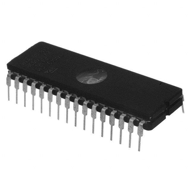
| 产品图片 |
|
| 产品型号 | CY7C1414KV18-250BZI |
| PCN组件/产地 | http://www.cypress.com/?docID=47156 |
| rohs | 含铅 / 不符合限制有害物质指令(RoHS)规范要求 |
| 产品系列 | - |
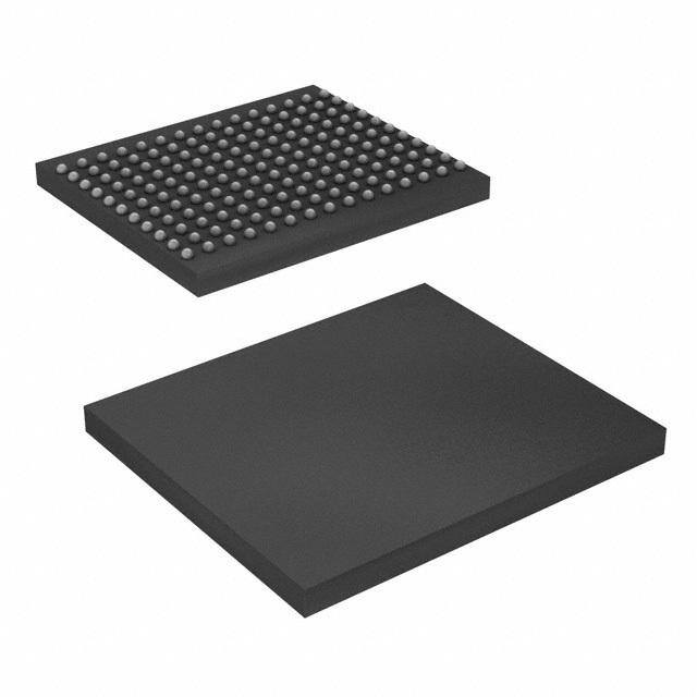
| 供应商器件封装 | 165-FBGA(13x15) |
| 其它名称 | CY7C1414KV18250BZI |
| 包装 | 托盘 |
| 存储器类型 | SRAM - 同步,QDR II |
| 存储容量 | 36M(1M x 36) |
| 封装/外壳 | 165-LBGA |
| 工作温度 | -40°C ~ 85°C |
| 接口 | 并联 |
| 标准包装 | 136 |
| 格式-存储器 | RAM |
| 电压-电源 | 1.7 V ~ 1.9 V |
| 速度 | 250MHz |


- 商务部:美国ITC正式对集成电路等产品启动337调查
- 曝三星4nm工艺存在良率问题 高通将骁龙8 Gen1或转产台积电
- 太阳诱电将投资9.5亿元在常州建新厂生产MLCC 预计2023年完工
- 英特尔发布欧洲新工厂建设计划 深化IDM 2.0 战略
- 台积电先进制程称霸业界 有大客户加持明年业绩稳了
- 达到5530亿美元!SIA预计今年全球半导体销售额将创下新高
- 英特尔拟将自动驾驶子公司Mobileye上市 估值或超500亿美元
- 三星加码芯片和SET,合并消费电子和移动部门,撤换高东真等 CEO
- 三星电子宣布重大人事变动 还合并消费电子和移动部门
- 海关总署:前11个月进口集成电路产品价值2.52万亿元 增长14.8%


PDF Datasheet 数据手册内容提取
CY7C1425KV18 CY7C1412KV18 CY7C1414KV18 ® 36-Mbit QDR II SRAM Two-Word Burst Architecture 36-Mbit QDR® II SRAM Two-Word Burst Architecture Features Configurations ■Separate independent read and write data ports CY7C1425KV18 – 4M × 9 ❐Supports concurrent transactions CY7C1412KV18 – 2M × 18 ■333 MHz clock for high bandwidth CY7C1414KV18 – 1M × 36 ■Two-word burst on all accesses Functional Description ■Double data rate (DDR) Interfaces on both read and write ports The CY7C1425KV18, CY7C1412KV18, and CY7C1414KV18 (data transferred at 666 MHz) at 333 MHz are 1.8 V synchronous pipelined SRAMs, equipped with QDR II ■Two input clocks (K and K) for precise DDR timing architecture. QDR II architecture consists of two separate ports: the read port and the write port to access the memory array. The ❐SRAM uses rising edges only read port has dedicated data outputs to support read operations ■Two input clocks for output data (C and C) to minimize clock and the write port has dedicated data inputs to support write skew and flight time mismatches operations. QDR II architecture has separate data inputs and data outputs to completely eliminate the need to “turnaround” the ■Echo clocks (CQ and CQ) simplify data capture in high speed data bus that exists with common I/O devices. Access to each systems port is through a common address bus. Addresses for read and ■Single multiplexed address input bus latches address inputs write addresses are latched on alternate rising edges of the input for both read and write ports (K) clock. Accesses to the QDR II read and write ports are completely independent of one another. To maximize data ■Separate port selects for depth expansion throughput, both read and write ports are equipped with DDR interfaces. Each address location is associated with two 9-bit ■Synchronous internally self-timed writes words (CY7C1425KV18), 18-bit words (CY7C1412KV18), or ■QDR® II operates with 1.5 cycle read latency when DOFF is 36-bit words (CY7C1414KV18) that burst sequentially into or out asserted HIGH of the device. Because data can be transferred into and out of the device on every rising edge of both input clocks (K and K and ■Operates similar to QDR I device with 1 cycle read latency when C and C), memory bandwidth is maximized while simplifying DOFF is asserted LOW system design by eliminating bus turnarounds. ■Available in × 9, × 18, and × 36 configurations Depth expansion is accomplished with port selects, which ■Full data coherency, providing most current data enables each port to operate independently. All synchronous inputs pass through input registers controlled by ■Core V = 1.8 V (±0.1 V); I/O V = 1.4 V to V DD DDQ DD the K or K input clocks. All data outputs pass through output ❐Supports both 1.5 V and 1.8 V I/O supply registers controlled by the C or C (or K or K in a single clock ■Available in 165-ball FBGA package (13 × 15 × 1.4 mm) domain) input clocks. Writes are conducted with on-chip synchronous self-timed write circuitry. ■Offered in both Pb-free and non Pb-free Packages For a complete list of related documentation, click here. ■Variable drive HSTL output buffers ■JTAG 1149.1 compatible test access port ■Phase locked loop (PLL) for accurate data placement Selection Guide Description 333 MHz 300 MHz 250 MHz Unit Maximum operating frequency 333 300 250 MHz Maximum operating current × 9 730 680 590 mA × 18 750 700 610 × 36 910 850 730 CypressSemiconductorCorporation • 198 Champion Court • SanJose, CA 95134-1709 • 408-943-2600 Document Number: 001-57825 Rev. *O Revised January 3, 2018
CY7C1425KV18 CY7C1412KV18 CY7C1414KV18 Logic Block Diagram – CY7C1425KV18 9 D [8:0] Write Write 21 Reg Reg Address A(20:0) 21 Address Register A(20:0) Register code 2M 2M code De x x De KK CGLeKn. Write Add. 9 Array 9 Array Read Add. CLoongtircol RCPS DOFF Read Data Reg. C CQ 18 VREF 9 9 CQ Reg. Reg. Control WPS Logic BWS[0] 9 Reg. 9 9 Q[8:0] Logic Block Diagram – CY7C1412KV18 18 D [17:0] Write Write 20 Reg Reg Address A(19:0) 20 Address Register A(19:0) Register de 1 1 de o M M o c c d. De x 18 x 18 d. De K CLK e Ad Arra Arra d Ad Control RPS K Gen. Writ y y Rea Logic C DOFF Read Data Reg. C CQ 36 VREF 18 18 CQ Reg. Reg. Control WPS Logic BWS[1:0] 18 Reg. 18 18 Q[17:0] Document Number: 001-57825 Rev. *O Page 2 of 33
CY7C1425KV18 CY7C1412KV18 CY7C1414KV18 Logic Block Diagram – CY7C1414KV18 36 D [35:0] Write Write 19 Reg Reg Address A(18:0) 19 Address Register A(18:0) Register ode 51 51 ode c 2 2 c e K K e d. D x 3 x 3 d. D KK CGLeKn. Write Ad 6 Array 6 Array Read Ad CLoongtircol RCPS DOFF Read Data Reg. C CQ 72 VREF 36 36 CQ Reg. Reg. Control WPS Logic BWS[3:0] 36 Reg. 36 36 Q[35:0] Document Number: 001-57825 Rev. *O Page 3 of 33
CY7C1425KV18 CY7C1412KV18 CY7C1414KV18 Contents Pin Configurations ...........................................................5 Instruction Codes ...........................................................19 Pin Definitions ..................................................................7 Boundary Scan Order ....................................................20 Functional Overview ........................................................8 Power Up Sequence in QDR II SRAM ...........................21 Read Operations .........................................................8 Power Up Sequence .................................................21 Write Operations .........................................................9 PLL Constraints .........................................................21 Byte Write Operations .................................................9 Maximum Ratings ...........................................................22 Concurrent Transactions .............................................9 Operating Range .............................................................22 Depth Expansion .........................................................9 Neutron Soft Error Immunity .........................................22 Programmable Impedance ..........................................9 Electrical Characteristics ...............................................22 Echo Clocks ................................................................9 DC Electrical Characteristics .....................................22 PLL ..............................................................................9 AC Electrical Characteristics .....................................24 Application Example ......................................................10 Capacitance ....................................................................24 Truth Table ......................................................................11 Thermal Resistance ........................................................24 Write Cycle Descriptions ...............................................11 AC Test Loads and Waveforms .....................................24 Write Cycle Descriptions ...............................................12 Switching Characteristics ..............................................25 Write Cycle Descriptions ...............................................12 Switching Waveforms ....................................................27 IEEE 1149.1 Serial Boundary Scan (JTAG) ..................13 Ordering Information ......................................................28 Disabling the JTAG Feature ......................................13 Ordering Code Definitions .........................................28 Test Access Port .......................................................13 Package Diagram ............................................................29 Performing a TAP Reset ...........................................13 Acronyms ........................................................................30 TAP Registers ...........................................................13 Document Conventions .................................................30 TAP Instruction Set ...................................................13 Units of Measure .......................................................30 TAP Controller State Diagram .......................................15 Document History Page .................................................31 TAP Controller Block Diagram ......................................16 Sales, Solutions, and Legal Information ......................33 TAP Electrical Characteristics ......................................16 Worldwide Sales and Design Support .......................33 TAP AC Switching Characteristics ...............................17 Products ....................................................................33 TAP Timing and Test Conditions ..................................18 PSoC® Solutions ......................................................33 Identification Register Definitions ................................19 Cypress Developer Community .................................33 Scan Register Sizes .......................................................19 Technical Support .....................................................33 Document Number: 001-57825 Rev. *O Page 4 of 33
CY7C1425KV18 CY7C1412KV18 CY7C1414KV18 Pin Configurations The pin configurations for CY7C1425KV18, CY7C1412KV18, and CY7C1414KV18 follow. [1] Figure 1. 165-ball FBGA (13 × 15 × 1.4 mm) pinout CY7C1425KV18 (4M × 9) 1 2 3 4 5 6 7 8 9 10 11 A CQ NC/72M A WPS NC K NC/144M RPS A A CQ B NC NC NC A NC/288M K BWS A NC NC Q4 0 C NC NC NC V A A A V NC NC D4 SS SS D NC D5 NC V V V V V NC NC NC SS SS SS SS SS E NC NC Q5 V V V V V NC D3 Q3 DDQ SS SS SS DDQ F NC NC NC V V V V V NC NC NC DDQ DD SS DD DDQ G NC D6 Q6 V V V V V NC NC NC DDQ DD SS DD DDQ H DOFF V V V V V V V V V ZQ REF DDQ DDQ DD SS DD DDQ DDQ REF J NC NC NC V V V V V NC Q2 D2 DDQ DD SS DD DDQ K NC NC NC V V V V V NC NC NC DDQ DD SS DD DDQ L NC Q7 D7 V V V V V NC NC Q1 DDQ SS SS SS DDQ M NC NC NC V V V V V NC NC D1 SS SS SS SS SS N NC D8 NC V A A A V NC NC NC SS SS P NC NC Q8 A A C A A NC D0 Q0 R TDO TCK A A A C A A A TMS TDI Note 1. NC/72M, NC/144M and NC/288M are not connected to the die and can be tied to any voltage level. Document Number: 001-57825 Rev. *O Page 5 of 33
CY7C1425KV18 CY7C1412KV18 CY7C1414KV18 Pin Configurations (continued) The pin configurations for CY7C1425KV18, CY7C1412KV18, and CY7C1414KV18 follow. [1] Figure 1. 165-ball FBGA (13 × 15 × 1.4 mm) pinout CY7C1412KV18 (2M × 18) 1 2 3 4 5 6 7 8 9 10 11 A CQ NC/144M A WPS BWS K NC/288M RPS A NC/72M CQ 1 B NC Q9 D9 A NC K BWS A NC NC Q8 0 C NC NC D10 V A A A V NC Q7 D8 SS SS D NC D11 Q10 V V V V V NC NC D7 SS SS SS SS SS E NC NC Q11 V V V V V NC D6 Q6 DDQ SS SS SS DDQ F NC Q12 D12 V V V V V NC NC Q5 DDQ DD SS DD DDQ G NC D13 Q13 V V V V V NC NC D5 DDQ DD SS DD DDQ H DOFF V V V V V V V V V ZQ REF DDQ DDQ DD SS DD DDQ DDQ REF J NC NC D14 V V V V V NC Q4 D4 DDQ DD SS DD DDQ K NC NC Q14 V V V V V NC D3 Q3 DDQ DD SS DD DDQ L NC Q15 D15 V V V V V NC NC Q2 DDQ SS SS SS DDQ M NC NC D16 V V V V V NC Q1 D2 SS SS SS SS SS N NC D17 Q16 V A A A V NC NC D1 SS SS P NC NC Q17 A A C A A NC D0 Q0 R TDO TCK A A A C A A A TMS TDI CY7C1414KV18 (1M × 36) 1 2 3 4 5 6 7 8 9 10 11 A CQ NC/288M NC/72M WPS BWS K BWS RPS A NC/144M CQ 2 1 B Q27 Q18 D18 A BWS K BWS A D17 Q17 Q8 3 0 C D27 Q28 D19 V A A A V D16 Q7 D8 SS SS D D28 D20 Q19 V V V V V Q16 D15 D7 SS SS SS SS SS E Q29 D29 Q20 V V V V V Q15 D6 Q6 DDQ SS SS SS DDQ F Q30 Q21 D21 V V V V V D14 Q14 Q5 DDQ DD SS DD DDQ G D30 D22 Q22 V V V V V Q13 D13 D5 DDQ DD SS DD DDQ H DOFF V V V V V V V V V ZQ REF DDQ DDQ DD SS DD DDQ DDQ REF J D31 Q31 D23 V V V V V D12 Q4 D4 DDQ DD SS DD DDQ K Q32 D32 Q23 V V V V V Q12 D3 Q3 DDQ DD SS DD DDQ L Q33 Q24 D24 V V V V V D11 Q11 Q2 DDQ SS SS SS DDQ M D33 Q34 D25 V V V V V D10 Q1 D2 SS SS SS SS SS N D34 D26 Q25 V A A A V Q10 D9 D1 SS SS P Q35 D35 Q26 A A C A A Q9 D0 Q0 R TDO TCK A A A C A A A TMS TDI Document Number: 001-57825 Rev. *O Page 6 of 33
CY7C1425KV18 CY7C1412KV18 CY7C1414KV18 Pin Definitions Pin Name I/O Pin Description D Input- Data input signals. Sampled on the rising edge of K and K clocks during valid write operations. [x:0] synchronous CY7C1425KV18 D [8:0] CY7C1412KV18 D [17:0] CY7C1414KV18 D [35:0] WPS Input- Write port select active LOW. Sampled on the rising edge of the K clock. When asserted active, a synchronous write operation is initiated. Deasserting deselects the write port. Deselecting the write port ignores D . [x:0] BWS , Input- Byte write select 0, 1, 2, and 3 active LOW. Sampled on the rising edge of the K and K clocks during 0 BWS1, synchronous write operations. Used to select which byte is written into the device during the current portion of the BWS , write operations. Bytes not written remain unaltered. 2 BWS3 CY7C1425KV18 BWS0 controls D[8:0]. CY7C1412KV18 BWS controls D and BWS controls D 0 [8:0] 1 [17:9]. CY7C1414KV18 BWS controls D , BWS controls D , BWS controls D and BWS 0 [8:0] 1 [17:9] 2 [26:18] 3 controls D [35:27]. All the byte write selects are sampled on the same edge as the data. Deselecting a byte write select ignores the corresponding byte of data and it is not written into the device. A Input- Address inputs. Sampled on the rising edge of the K (read address) and K (write address) clocks during synchronous active read and write operations. These address inputs are multiplexed for both read and write operations. Internally, the device is organized as 4M × 9 (2 arrays each of 2M × 9) for CY7C1425KV18, 2M × 18 (2 arrays each of 1M × 18) for CY7C1412KV18, and 1M × 36 (2 arrays each of 512K × 36) for CY7C1414KV18. Therefore, only 21 address inputs are needed to access the entire memory array of CY7C1425KV18, 20 address inputs for CY7C1412KV18, and 19 address inputs for CY7C1414KV18. These inputs are ignored when the appropriate port is deselected. Q Output- Data output signals. These pins drive out the requested data during a read operation. Valid data is [x:0] synchronous driven out on the rising edge of the C and C clocks during read operations, or K and K when in single clock mode. When the read port is deselected, Q are automatically tristated. [x:0] CY7C1425KV18 Q [8:0] CY7C1412KV18 Q [17:0] CY7C1414KV18 Q [35:0] RPS Input- Read port select active LOW. Sampled on the rising edge of positive input clock (K). When active, a synchronous read operation is initiated. Deasserting deselects the read port. When deselected, the pending access is allowed to complete and the output drivers are automatically tristated following the next rising edge of the C clock. Each read access consists of a burst of two sequential transfers. C Input clock Positive input clock for output data. C is used in conjunction with C to clock out the read data from the device. Use C and C together to deskew the flight times of various devices on the board back to the controller. See Application Example on page 10 for further details. C Input clock Negative input clock for output data. C is used in conjunction with C to clock out the read data from the device. Use C and C together to deskew the flight times of various devices on the board back to the controller. See Application Example on page 10 for further details. K Input clock Positive input clock input. The rising edge of K is used to capture synchronous inputs to the device and to drive out data through Q when in single clock mode. All accesses are initiated on the rising [x:0] edge of K. K Input clock Negative input clock input. K is used to capture synchronous inputs being presented to the device and to drive out data through Q when in single clock mode. [x:0] CQ Echo clock CQ referenced with respect to C. This is a free running clock and is synchronized to the input clock for output data (C) of the QDR II. In single clock mode, CQ is generated with respect to K. The timing for the echo clocks is shown in Switching Characteristics on page 25. CQ Echo clock CQ referenced with respect to C. This is a free running clock and is synchronized to the input clock for output data (C) of the QDR II. In single clock mode, CQ is generated with respect to K. The timing for the echo clocks is shown in the Switching Characteristics on page 25. Document Number: 001-57825 Rev. *O Page 7 of 33
CY7C1425KV18 CY7C1412KV18 CY7C1414KV18 Pin Definitions (continued) Pin Name I/O Pin Description ZQ Input Output impedance matching input. This input is used to tune the device outputs to the system data bus impedance. CQ, CQ, and Q output impedance are set to 0.2 × RQ, where RQ is a resistor [x:0] connected between ZQ and ground. Alternatively, connect this pin directly to V , which enables the DDQ minimum impedance mode. This pin cannot be connected directly to GND or left unconnected. DOFF Input PLL turn off active LOW. Connecting this pin to ground turns off the PLL inside the device. The timing in the operation with the PLL turned off differs from those listed in this data sheet. For normal operation, connect this pin to a pull up through a 10 K or less pull-up resistor. The device behaves in QDR I mode when the PLL is turned off. In this mode, the device can be operated at a frequency of up to 167 MHz with QDR I timing. TDO Output TDO pin for JTAG. TCK Input TCK pin for JTAG. TDI Input TDI pin for JTAG. TMS Input TMS pin for JTAG. NC N/A Not connected to the die. Can be tied to any voltage level. NC/72M Input Not connected to the die. Can be tied to any voltage level. NC/144M Input Not connected to the die. Can be tied to any voltage level. NC/288M Input Not connected to the die. Can be tied to any voltage level. V Input- Reference voltage input. Static input used to set the reference level for HSTL inputs, outputs, and AC REF reference measurement points. V Power supply Power supply inputs to the core of the device. DD V Ground Ground for the device. SS V Power supply Power supply inputs for the outputs of the device. DDQ Functional Overview rising edge of the output clocks (C and C, or K and K when in single clock mode). The CY7C1425KV18, CY7C1412KV18, and CY7C1414KV18 All synchronous control (RPS, WPS, BWS ) inputs pass [x:0] are synchronous pipelined burst SRAMs with a read port and a through input registers controlled by the rising edge of the input write port. The read port is dedicated to read operations and the clocks (K and K). write port is dedicated to write operations. Data flows into the SRAM through the write port and flows out through the read port. CY7C1412KV18 is described in the following sections. The same basic descriptions apply to CY7C1425KV18, and These devices multiplex the address inputs to minimize the number of address pins required. By having separate read and CY7C1414KV18. write ports, the QDR II completely eliminates the need to turn Read Operations around the data bus and avoids any possible data contention, thereby simplifying system design. Each access consists of two The CY7C1412KV18 is organized internally as two arrays of 9-bit data transfers in the case of CY7C1425KV18, two 18-bit 1M× 18. Accesses are completed in a burst of two sequential data transfers in the case of CY7C1412KV18, and two 36-bit 18-bit data words. Read operations are initiated by asserting data transfers in the case of CY7C1414KV18 in one clock cycle. RPSactive at the rising edge of the positive input clock (K). The address is latched on the rising edge of the K clock. The address This device operates with a read latency of one and half cycles presented to the address inputs is stored in the read address when DOFF pin is tied HIGH. When DOFF pin is set LOW or register. Following the next K clock rise, the corresponding connected to V then the device behaves in QDR I mode with SS lowest order 18-bit word of data is driven onto the Q using a read latency of one clock cycle. [17:0] C as the output timing reference. On the subsequent rising edge Accesses for both ports are initiated on the rising edge of the of C, the next 18-bit data word is driven onto the Q . The [17:0] positive input clock (K). All synchronous input timing is requested data is valid 0.45 ns from the rising edge of the output referenced from the rising edge of the input clocks (K and K) and clock (C and C or K and K when in single clock mode). all output timing is referenced to the output clocks (C and C, or Synchronous internal circuitry automatically tristates the outputs K and K when in single clock mode). following the next rising edge of the output clocks (C/C). This All synchronous data inputs (D[x:0]) pass through input registers enables for a seamless transition between devices without the controlled by the input clocks (K and K). All synchronous data insertion of wait states in a depth expanded memory. outputs (Q ) pass through output registers controlled by the [x:0] Document Number: 001-57825 Rev. *O Page 8 of 33
CY7C1425KV18 CY7C1412KV18 CY7C1414KV18 Write Operations on the rising edge of the positive input clock only (K). Each port select input can deselect the specified port. Deselecting a port Write operations are initiated by asserting WPS active at the does not affect the other port. All pending transactions (read and rising edge of the positive input clock (K). On the same K clock write) are completed before the device is deselected. rise the data presented to D is latched and stored into the [17:0] lower 18-bit write data register, provided BWS[1:0] are both Programmable Impedance asserted active. On the subsequent rising edge of the negative input clock (K), the address is latched and the information An external resistor, RQ, must be connected between the ZQ pin presented to D[17:0] is also stored into the write data register, on the SRAM and VSS to enable the SRAM to adjust its output provided BWS are both asserted active. The 36 bits of data driver impedance. The value of RQ must be 5X the value of the [1:0] are then written into the memory array at the specified location. intended line impedance driven by the SRAM. The allowable range of RQ to guarantee impedance matching with a tolerance When deselected, the write port ignores all inputs after the pending write operations are completed. of ±15% is between 175 and 350 , with VDDQ=1.5 V. The output impedance is adjusted every 1024 cycles upon power-up to account for drifts in supply voltage and temperature. Byte Write Operations Byte write operations are supported by the CY7C1412KV18. A Echo Clocks write operation is initiated as described in the Write Operations Echo clocks are provided on the QDR II to simplify data capture section. The bytes that are written are determined by BWS and 0 on high speed systems. Two echo clocks are generated by the BWS , which are sampled with each set of 18-bit data words. 1 QDR II. CQ is referenced with respect to C and CQ is referenced Asserting the appropriate byte write select input during the data with respect to C. These are free running clocks and are portion of a write latches the data being presented and writes it synchronized to the output clock of the QDR II. In the single clock into the device. Deasserting the byte write select input during the mode, CQ is generated with respect to K and CQ is generated data portion of a write enables the data stored in the device for with respect to K. The timing for the echo clocks is shown in that byte to remain unaltered. This feature is used to simplify Switching Characteristics on page 25. read, modify, or write operations to a byte write operation. PLL Concurrent Transactions These chips use a PLL which is designed to function between The read and write ports on the CY7C1412KV18 operate 120 MHz and the specified maximum clock frequency. During completely independently of one another. As each port latches power up, when the DOFF is tied HIGH, the PLL is locked after the address inputs on different clock edges, the user can read or 20 s of stable clock. The PLL can also be reset by slowing or write to any location, regardless of the transaction on the other stopping the input clocks K and K for a minimum of 30 ns. port. The user can start reads and writes in the same clock cycle. However, it is not necessary to reset the PLL to lock to the If the ports access the same location at the same time, the SRAM desired frequency. The PLL automatically locks 20 s after a delivers the most recent information associated with the stable clock is presented. The PLL may be disabled by applying specified address location. This includes forwarding data from a ground to the DOFF pin. When the PLL is turned off, the device write cycle that was initiated on the previous K clock rise. behaves in QDR I mode (with one cycle latency and a longer access time). Depth Expansion The CY7C1412KV18 has a port select input for each port. This enables for easy depth expansion. Both port selects are sampled Document Number: 001-57825 Rev. *O Page 9 of 33
CY7C1425KV18 CY7C1412KV18 CY7C1414KV18 Application Example Figure2 shows two QDR II used in an application. Figure 2. Application Example (Width Expansion) ZQ ZQ SRAM#1 SRAM#2 CQ/CQ CQ/CQ RQ RQ D[x:0] D[x:0] Q[x:0] Q[x:0] A RPS WPSBWS C C K K A RPSWPSBWS C C K K DATA IN[2x:0] DATA OUT [2x:0] ADDRESS RPS WPS BWS CLKIN1/CLKIN1 CLKIN2/CLKIN2 SOURCE K SOURCE K DELAYED K DELAYED K FPGA / ASIC Document Number: 001-57825 Rev. *O Page 10 of 33
CY7C1425KV18 CY7C1412KV18 CY7C1414KV18 Truth Table The truth table for CY7C1425KV18, CY7C1412KV18, and CY7C1414KV18 follow. [2, 3, 4, 5, 6, 7] Operation K RPS WPS DQ DQ Write cycle: L–H X L D(A + 0) at K(t) D(A + 1) at K(t) Load address on the rising edge of K; input write data on K and K rising edges. Read cycle: L–H L X Q(A + 0) at C(t + 1) Q(A + 1) at C(t + 2) Load address on the rising edge of K; wait one and a half cycle; read data on C and C rising edges. NOP: No operation L–H H H D = X D = X Q = high Z Q = high Z Standby: Clock stopped Stopped X X Previous state Previous state Write Cycle Descriptions The write cycle description table for CY7C1412KV18 follow. [2, 8] BWS0 BWS1 K K Comments L L L–H – During the data portion of a write sequence CY7C1412KV18 both bytes (D ) are written into the device. [17:0] L L – L–H During the data portion of a write sequence: CY7C1412KV18 both bytes (D ) are written into the device. [17:0] L H L–H – During the data portion of a write sequence: CY7C1412KV18 only the lower byte (D ) is written into the device, D remains unaltered. [8:0] [17:9] L H – L–H During the data portion of a write sequence CY7C1412KV18 only the lower byte (D ) is written into the device, D remains unaltered. [8:0] [17:9] H L L–H – During the data portion of a write sequence CY7C1412KV18 only the upper byte (D ) is written into the device, D remains unaltered. [17:9] [8:0] H L – L–H During the data portion of a write sequence CY7C1412KV18 only the upper byte (D ) is written into the device, D remains unaltered. [17:9] [8:0] H H L–H – No data is written into the devices during this portion of a write operation. H H – L–H No data is written into the devices during this portion of a write operation. Notes 2. X = “Don't Care,” H = Logic HIGH, L = Logic LOW, represents rising edge. 3. Device powers up deselected with the outputs in a tristate condition. 4. “A” represents address location latched by the devices when transaction was initiated. A + 0, A + 1 represents the internal address sequence in the burst. 5. “t” represents the cycle at which a read/write operation is started. t + 1, and t + 2 are the first, and second clock cycles respectively succeeding the “t” clock cycle. 6. Data inputs are registered at K and K rising edges. Data outputs are delivered on C and C rising edges, except when in single clock mode. 7. Ensure that when the clock is stopped K = K and C = C = HIGH. This is not essential, but permits most rapid restart by overcoming transmission line charging symmetrically. 8. Is based on a write cycle that was initiated in accordance with the Truth Table. BWS0, BWS1, BWS2, and BWS3 can be altered on different portions of a write cycle, as long as the setup and hold requirements are achieved. Document Number: 001-57825 Rev. *O Page 11 of 33
CY7C1425KV18 CY7C1412KV18 CY7C1414KV18 Write Cycle Descriptions The write cycle description table for CY7C1425KV18 follow. [9, 10] BWS K K Comments 0 L L–H – During the data portion of a write sequence, the single byte (D ) is written into the device. [8:0] L – L–H During the data portion of a write sequence, the single byte (D ) is written into the device. [8:0] H L–H – No data is written into the device during this portion of a write operation. H – L–H No data is written into the device during this portion of a write operation. Write Cycle Descriptions The write cycle description table for CY7C1414KV18 follow. [9, 10] BWS BWS BWS BWS K K Comments 0 1 2 3 L L L L L–H – During the data portion of a write sequence, all four bytes (D ) are written into [35:0] the device. L L L L – L–H During the data portion of a write sequence, all four bytes (D ) are written into [35:0] the device. L H H H L–H – During the data portion of a write sequence, only the lower byte (D ) is written [8:0] into the device. D remains unaltered. [35:9] L H H H – L–H During the data portion of a write sequence, only the lower byte (D ) is written [8:0] into the device. D remains unaltered. [35:9] H L H H L–H – During the data portion of a write sequence, only the byte (D ) is written into the [17:9] device. D and D remains unaltered. [8:0] [35:18] H L H H – L–H During the data portion of a write sequence, only the byte (D ) is written into the [17:9] device. D and D remains unaltered. [8:0] [35:18] H H L H L–H – During the data portion of a write sequence, only the byte (D ) is written into [26:18] the device. D and D remains unaltered. [17:0] [35:27] H H L H – L–H During the data portion of a write sequence, only the byte (D ) is written into [26:18] the device. D and D remains unaltered. [17:0] [35:27] H H H L L–H – During the data portion of a write sequence, only the byte (D ) is written into [35:27] the device. D remains unaltered. [26:0] H H H L – L–H During the data portion of a write sequence, only the byte (D ) is written into [35:27] the device. D remains unaltered. [26:0] H H H H L–H – No data is written into the device during this portion of a write operation. H H H H – L–H No data is written into the device during this portion of a write operation. Notes 9. X = “Don't Care,” H = Logic HIGH, L = Logic LOW, represents rising edge. 10.Is based on a write cycle that was initiated in accordance with the Truth Table on page 11. BWS0, BWS1, BWS2, and BWS3 can be altered on different portions of a write cycle, as long as the setup and hold requirements are achieved. Document Number: 001-57825 Rev. *O Page 12 of 33
CY7C1425KV18 CY7C1412KV18 CY7C1414KV18 IEEE 1149.1 Serial Boundary Scan (JTAG) Instruction Register Three-bit instructions are serially loaded into the instruction These SRAMs incorporate a serial boundary scan test access register. This register is loaded when it is placed between the TDI port (TAP) in the FBGA package. This part is fully compliant with and TDO pins, as shown in TAP Controller Block Diagram on IEEE Standard #1149.1-2001. The TAP operates using JEDEC page 16. Upon power-up, the instruction register is loaded with standard 1.8 V I/O logic levels. the IDCODE instruction. It is also loaded with the IDCODE instruction if the controller is placed in a reset state, as described Disabling the JTAG Feature in the previous section. It is possible to operate the SRAM without using the JTAG When the TAP controller is in the Capture-IR state, the two least feature. To disable the TAP controller, TCK must be tied LOW significant bits are loaded with a binary “01” pattern to enable (V ) to prevent clocking of the device. TDI and TMS are SS fault isolation of the board level serial test path. internally pulled up and may be unconnected. They may alternatively be connected to VDD through a pull-up resistor. TDO Bypass Register must be left unconnected. Upon power-up, the device comes up To save time when serially shifting data through registers, it is in a reset state, which does not interfere with the operation of the sometimes advantageous to skip certain chips. The bypass device. register is a single-bit register that can be placed between TDI Test Access Port and TDO pins. This enables shifting of data through the SRAM with minimal delay. The bypass register is set LOW (V ) when SS Test Clock the BYPASS instruction is executed. The test clock is used only with the TAP controller. All inputs are Boundary Scan Register captured on the rising edge of TCK. All outputs are driven from The boundary scan register is connected to all of the input and the falling edge of TCK. output pins on the SRAM. Several No Connect (NC) pins are also Test Mode Select (TMS) included in the scan register to reserve pins for higher density devices. The TMS input is used to give commands to the TAP controller and is sampled on the rising edge of TCK. This pin may be left The boundary scan register is loaded with the contents of the unconnected if the TAP is not used. The pin is pulled up RAM input and output ring when the TAP controller is in the internally, resulting in a logic HIGH level. Capture-DR state and is then placed between the TDI and TDO pins when the controller is moved to the Shift-DR state. The Test Data-In (TDI) EXTEST, SAMPLE/PRELOAD, and SAMPLE Z instructions are used to capture the contents of the input and output ring. The TDI pin is used to serially input information into the registers and can be connected to the input of any of the registers. The The Boundary Scan Order on page 20 shows the order in which register between TDI and TDO is chosen by the instruction that the bits are connected. Each bit corresponds to one of the bumps is loaded into the TAP instruction register. For information about on the SRAM package. The MSB of the register is connected to loading the instruction register, see the TAP Controller State TDI, and the LSB is connected to TDO. Diagram on page 15. TDI is internally pulled up and can be unconnected if the TAP is unused in an application. TDI is Identification (ID) Register connected to the most significant bit (MSB) on any register. The ID register is loaded with a vendor-specific, 32-bit code during the Capture-DR state when the IDCODE command is Test Data-Out (TDO) loaded in the instruction register. The IDCODE is hardwired into The TDO output pin is used to serially clock data out from the the SRAM and can be shifted out when the TAP controller is in registers. The output is active, depending upon the current state the Shift-DR state. The ID register has a vendor code and other of the TAP state machine (see Instruction Codes on page 19). information described in Identification Register Definitions on The output changes on the falling edge of TCK. TDO is page 19. connected to the least significant bit (LSB) of any register. TAP Instruction Set Performing a TAP Reset Eight different instructions are possible with the three-bit A Reset is performed by forcing TMS HIGH (VDD) for five rising instruction register. All combinations are listed in Instruction edges of TCK. This Reset does not affect the operation of the Codes on page 19. Three of these instructions are listed as SRAM and is performed when the SRAM is operating. At power RESERVED and must not be used. The other five instructions up, the TAP is reset internally to ensure that TDO comes up in a are described in this section in detail. high Z state. Instructions are loaded into the TAP controller during the Shift-IR TAP Registers state when the instruction register is placed between TDI and TDO. During this state, instructions are shifted through the Registers are connected between the TDI and TDO pins to scan instruction register through the TDI and TDO pins. To execute the data in and out of the SRAM test circuitry. Only one register the instruction after it is shifted in, the TAP controller must be can be selected at a time through the instruction registers. Data moved into the Update-IR state. is serially loaded into the TDI pin on the rising edge of TCK. Data is output on the TDO pin on the falling edge of TCK. Document Number: 001-57825 Rev. *O Page 13 of 33
CY7C1425KV18 CY7C1412KV18 CY7C1414KV18 IDCODE BYPASS The IDCODE instruction loads a vendor-specific, 32-bit code into When the BYPASS instruction is loaded in the instruction register the instruction register. It also places the instruction register and the TAP is placed in a Shift-DR state, the bypass register is between the TDI and TDO pins and shifts the IDCODE out of the placed between the TDI and TDO pins. The advantage of the device when the TAP controller enters the Shift-DR state. The BYPASS instruction is that it shortens the boundary scan path IDCODE instruction is loaded into the instruction register at when multiple devices are connected together on a board. power up or whenever the TAP controller is supplied a Test-Logic-Reset state. EXTEST The EXTEST instruction drives the preloaded data out through SAMPLE Z the system output pins. This instruction also connects the The SAMPLE Z instruction connects the boundary scan register boundary scan register for serial access between the TDI and between the TDI and TDO pins when the TAP controller is in a TDO in the Shift-DR controller state. Shift-DR state. The SAMPLE Z command puts the output bus into a high Z state until the next command is supplied during the EXTEST OUTPUT BUS TRISTATE Update IR state. IEEE Standard 1149.1 mandates that the TAP controller be able to put the output bus into a tristate mode. SAMPLE/PRELOAD The boundary scan register has a special bit located at bit #108. SAMPLE/PRELOAD is a 1149.1 mandatory instruction. When When this scan cell, called the “extest output bus tristate,” is the SAMPLE/PRELOAD instructions are loaded into the latched into the preload register during the Update-DR state in instruction register and the TAP controller is in the Capture-DR the TAP controller, it directly controls the state of the output state, a snapshot of data on the input and output pins is captured (Q-bus) pins, when the EXTEST is entered as the current in the boundary scan register. instruction. When HIGH, it enables the output buffers to drive the The TAP controller clock can only operate at a frequency up to output bus. When LOW, this bit places the output bus into a 20 MHz, while the SRAM clock operates more than an order of highZ condition. magnitude faster. Because there is a large difference in the clock This bit is set by entering the SAMPLE/PRELOAD or EXTEST frequencies, it is possible that during the Capture-DR state, an command, and then shifting the desired bit into that cell, during input or output undergoes a transition. The TAP may then try to the Shift-DR state. During Update-DR, the value loaded into that capture a signal while in transition (metastable state). This does shift-register cell latches into the preload register. When the not harm the device, but there is no guarantee as to the value EXTEST instruction is entered, this bit directly controls the output that is captured. Repeatable results may not be possible. Q-bus pins. Note that this bit is pre-set LOW to enable the output To guarantee that the boundary scan register captures the when the device is powered up, and also when the TAP controller correct value of a signal, the SRAM signal must be stabilized is in the Test-Logic-Reset state. long enough to meet the TAP controller’s capture setup plus hold times (t and t ). The SRAM clock input might not be captured Reserved CS CH correctly if there is no way in a design to stop (or slow) the clock These instructions are not implemented but are reserved for during a SAMPLE/PRELOAD instruction. If this is an issue, it is future use. Do not use these instructions. still possible to capture all other signals and simply ignore the value of the CK and CK captured in the boundary scan register. After the data is captured, it is possible to shift out the data by putting the TAP into the Shift-DR state. This places the boundary scan register between the TDI and TDO pins. PRELOAD places an initial data pattern at the latched parallel outputs of the boundary scan register cells before the selection of another boundary scan test operation. The shifting of data for the SAMPLE and PRELOAD phases can occur concurrently when required, that is, while the data captured is shifted out, the preloaded data can be shifted in. Document Number: 001-57825 Rev. *O Page 14 of 33
CY7C1425KV18 CY7C1412KV18 CY7C1414KV18 TAP Controller State Diagram The state diagram for the TAP controller follows. [11] TEST-LOGIC 1 RESET 0 1 TEST-LOGIC/ 1 SELECT 1 SELECT 0 IDLE DR-SCAN IR-SCAN 0 0 1 1 CAPTURE-DR CAPTURE-IR 0 0 SHIFT-DR 0 SHIFT-IR 0 1 1 1 1 EXIT1-DR EXIT1-IR 0 0 PAUSE-DR 0 PAUSE-IR 0 1 1 0 0 EXIT2-DR EXIT2-IR 1 1 UPDATE-DR UPDATE-IR 1 1 0 0 Note 11.The 0/1 next to each state represents the value at TMS at the rising edge of TCK. Document Number: 001-57825 Rev. *O Page 15 of 33
CY7C1425KV18 CY7C1412KV18 CY7C1414KV18 TAP Controller Block Diagram 0 Bypass Register 2 1 0 TDI Selection Instruction Register Selection TDO Circuitry Circuitry 31 30 29 . . 2 1 0 Identification Register 108 . . . . 2 1 0 Boundary Scan Register TCK TAP Controller TMS TAP Electrical Characteristics Over the Operating Range Parameter [12, 13, 14] Description Test Conditions Min Max Unit V Output HIGH voltage I =2.0 mA 1.4 – V OH1 OH V Output HIGH voltage I =100 A 1.6 – V OH2 OH V Output LOW voltage I = 2.0 mA – 0.4 V OL1 OL V Output LOW voltage I = 100 A – 0.2 V OL2 OL V Input HIGH voltage 0.65 × V V + 0.3 V IH DD DD V Input LOW voltage –0.3 0.35 × V V IL DD I Input and output load current GND V V –5 5 A X I DD Notes 12.These characteristics pertain to the TAP inputs (TMS, TCK, TDI and TDO). Parallel load levels are specified in the Electrical Characteristics on page 22. 13.Overshoot: VIH(AC) < VDDQ + 0.85 V (Pulse width less than tCYC/2), Undershoot: VIL(AC) > 1.5 V (Pulse width less than tCYC/2). 14.All voltage referenced to Ground. Document Number: 001-57825 Rev. *O Page 16 of 33
CY7C1425KV18 CY7C1412KV18 CY7C1414KV18 TAP AC Switching Characteristics Over the Operating Range Parameter [15, 16] Description Min Max Unit t TCK clock cycle time 50 – ns TCYC t TCK clock frequency – 20 MHz TF t TCK clock HIGH 20 – ns TH t TCK clock LOW 20 – ns TL Setup Times t TMS setup to TCK clock rise 5 – ns TMSS t TDI setup to TCK clock rise 5 – ns TDIS t Capture setup to TCK rise 5 – ns CS Hold Times t TMS hold after TCK clock rise 5 – ns TMSH t TDI hold after clock rise 5 – ns TDIH t Capture hold after clock rise 5 – ns CH Output Times t TCK clock LOW to TDO valid – 10 ns TDOV t TCK clock LOW to TDO invalid 0 – ns TDOX Notes 15.tCS and tCH refer to the setup and hold time requirements of latching data from the boundary scan register. 16.Test conditions are specified using the load in TAP AC Test Conditions. tR/tF = 1 ns. Document Number: 001-57825 Rev. *O Page 17 of 33
CY7C1425KV18 CY7C1412KV18 CY7C1414KV18 TAP Timing and Test Conditions Figure3 shows the TAP timing and test conditions. [17] Figure 3. TAP Timing and Test Conditions 0.9V ALL INPUT PULSES 1.8V 50 0.9V TDO 0V Z0= 50 CL= 20 pF (a) GND tTH tTL Test Clock TCK t TCYC t TMSH t TMSS Test Mode Select TMS t TDIS t TDIH Test Data In TDI Test Data Out TDO tTDOV tTDOX Note 17.Test conditions are specified using the load in TAP AC Test Conditions. tR/tF = 1 ns. Document Number: 001-57825 Rev. *O Page 18 of 33
CY7C1425KV18 CY7C1412KV18 CY7C1414KV18 Identification Register Definitions Value Instruction Field Description CY7C1425KV18 CY7C1412KV18 CY7C1414KV18 Revision number (31:29) 000 000 000 Version number. Cypress device ID (28:12) 11010011010001111 11010011010010111 11010011010100111 Defines the type of SRAM. Cypress JEDEC ID (11:1) 00000110100 00000110100 00000110100 Allows unique identification of SRAM vendor. ID register presence (0) 1 1 1 Indicates the presence of an ID register. Scan Register Sizes Register Name Bit Size Instruction 3 Bypass 1 ID 32 Boundary scan 109 Instruction Codes Instruction Code Description EXTEST 000 Captures the input and output ring contents. IDCODE 001 Loads the ID register with the vendor ID code and places the register between TDI and TDO. This operation does not affect SRAM operation. SAMPLE Z 010 Captures the input and output contents. Places the boundary scan register between TDI and TDO. Forces all SRAM output drivers to a high Z state. RESERVED 011 Do Not Use: This instruction is reserved for future use. SAMPLE/PRELOAD 100 Captures the input and output contents. Places the boundary scan register between TDI and TDO. Does not affect the SRAM operation. RESERVED 101 Do Not Use: This instruction is reserved for future use. RESERVED 110 Do Not Use: This instruction is reserved for future use. BYPASS 111 Places the bypass register between TDI and TDO. This operation does not affect SRAM operation. Document Number: 001-57825 Rev. *O Page 19 of 33
CY7C1425KV18 CY7C1412KV18 CY7C1414KV18 Boundary Scan Order Bit # Bump ID Bit # Bump ID Bit # Bump ID Bit # Bump ID 0 6R 28 10G 56 6A 84 1J 1 6P 29 9G 57 5B 85 2J 2 6N 30 11F 58 5A 86 3K 3 7P 31 11G 59 4A 87 3J 4 7N 32 9F 60 5C 88 2K 5 7R 33 10F 61 4B 89 1K 6 8R 34 11E 62 3A 90 2L 7 8P 35 10E 63 2A 91 3L 8 9R 36 10D 64 1A 92 1M 9 11P 37 9E 65 2B 93 1L 10 10P 38 10C 66 3B 94 3N 11 10N 39 11D 67 1C 95 3M 12 9P 40 9C 68 1B 96 1N 13 10M 41 9D 69 3D 97 2M 14 11N 42 11B 70 3C 98 3P 15 9M 43 11C 71 1D 99 2N 16 9N 44 9B 72 2C 100 2P 17 11L 45 10B 73 3E 101 1P 18 11M 46 11A 74 2D 102 3R 19 9L 47 10A 75 2E 103 4R 20 10L 48 9A 76 1E 104 4P 21 11K 49 8B 77 2F 105 5P 22 10K 50 7C 78 3F 106 5N 23 9J 51 6C 79 1G 107 5R 24 9K 52 8A 80 1F 108 Internal 25 10J 53 7A 81 3G 26 11J 54 7B 82 2G 27 11H 55 6B 83 1H Document Number: 001-57825 Rev. *O Page 20 of 33
CY7C1425KV18 CY7C1412KV18 CY7C1414KV18 Power Up Sequence in QDR II SRAM PLL Constraints ■PLL uses K clock as its synchronizing input. The input must QDR II SRAMs must be powered up and initialized in a have low phase jitter, which is specified as t . predefined manner to prevent undefined operations. KC Var ■The PLL functions at frequencies down to 120 MHz. Power Up Sequence ■If the input clock is unstable and the PLL is enabled, then the ■Apply power and drive DOFF either HIGH or LOW (All other PLL may lock onto an incorrect frequency, causing unstable inputs can be HIGH or LOW). SRAM behavior. To avoid this, provide 20 s of stable clock to ❐Apply VDD before VDDQ. relock to the desired clock frequency. ❐Apply V before V or at the same time as V . DDQ REF REF ❐Drive DOFF HIGH. ■Provide stable DOFF (HIGH), power and clock (K, K) for 20 s to lock the PLL. Figure 4. Power Up Waveforms ~~ K K ~~ Unstable Clock > 20μs Stable clock Start Normal Operation Clock Start (Clock Starts after V D D / V D D Q Stable) VDD/VDDQ VDD/ VDDQ Stable (< +/- 0.1V DC per 50ns ) Fix HIGH (or tie to V ) DDQ DOFF Document Number: 001-57825 Rev. *O Page 21 of 33
CY7C1425KV18 CY7C1412KV18 CY7C1414KV18 Maximum Ratings Operating Range Exceeding maximum ratings may impair the useful life of the Ambient device. These user guidelines are not tested. Range Temperature (T ) V [19] V [19] A DD DDQ Storage temperature ................................–65 °C to +150 °C Commercial 0 °C to +70 °C 1.8 ± 0.1 V 1.4 V to Ambient temperature Industrial –40 °C to +85 °C VDD with power applied ...................................–55 °C to +125 °C Supply voltage on V relative to GND .......–0.5 V to +2.9 V DD Neutron Soft Error Immunity Supply voltage on V relative to GND ......–0.5 V to +V DDQ DD DC applied to outputs in high Z ........–0.5 V to VDDQ + 0.5 V Parameter Description Test Typ Max* Unit DC input voltage [18] ...........................–0.5 V to V + 0.5 V Conditions DD Current into outputs (LOW) ........................................20 mA LSBU Logical 25 °C 197 216 FIT/ single-bit Mb Static discharge voltage upsets (MIL-STD-883, M. 3015) .........................................> 2001 V LMBU Logical 25 °C 0 0.01 FIT/ Latch-up current ....................................................> 200 mA Multi-Bit Mb upsets SEL Single event 85 °C 0 0.1 FIT/ latchup Dev * No LMBU or SEL events occurred during testing; this column represents a statistical 2, 95% confidence limit calculation. For more details refer to Application Note AN54908 “Accelerated Neutron SER Testing and Calculation of Terrestrial Failure Rates”. Electrical Characteristics Over the Operating Range DC Electrical Characteristics Over the Operating Range Parameter [20] Description Test Conditions Min Typ Max Unit V Power supply voltage 1.7 1.8 1.9 V DD V I/O supply voltage 1.4 1.5 V V DDQ DD V Output HIGH voltage Note 21 V /2 – 0.12 – V /2 + 0.12 V OH DDQ DDQ V Output LOW voltage Note 22 V /2 – 0.12 – V /2 + 0.12 V OL DDQ DDQ V Output HIGH voltage I =0.1 mA, nominal impedance V – 0.2 – V V OH(LOW) OH DDQ DDQ V Output LOW voltage I = 0.1 mA, nominal impedance V – 0.2 V OL(LOW) OL SS V Input HIGH voltage V + 0.1 – V + 0.3 V IH REF DDQ V Input LOW voltage –0.3 – V – 0.1 V IL REF I Input leakage current GND V V 5 – 5 A X I DDQ I Output leakage current GND V V output disabled 5 – 5 A OZ I DDQ, V Input reference voltage [23] Typical value = 0.75 V 0.68 0.75 0.95 V REF Notes 18.Overshoot: VIH(AC) < VDDQ + 0.85 V (Pulse width less than tCYC/2), Undershoot: VIL(AC) > 1.5 V (Pulse width less than tCYC/2). 19.Power-up: Assumes a linear ramp from 0 V to VDD(min) within 200 ms. During this time VIH < VDD and VDDQ VDD. 20.All voltage referenced to Ground. 21.Output are impedance controlled. IOH = (VDDQ/2)/(RQ/5) for values of 175 RQ 350 . 22.Output are impedance controlled. IOL = (VDDQ/2)/(RQ/5) for values of 175 RQ 350 . 23.VREF(min) = 0.68 V or 0.46 VDDQ, whichever is larger, VREF(max) = 0.95 V or 0.54 VDDQ, whichever is smaller. Document Number: 001-57825 Rev. *O Page 22 of 33
CY7C1425KV18 CY7C1412KV18 CY7C1414KV18 Electrical Characteristics (continued) Over the Operating Range DC Electrical Characteristics (continued) Over the Operating Range Parameter [20] Description Test Conditions Min Typ Max Unit I [24] V operating supply V = Max, I = 0 mA, 333 MHz (× 9) – – 730 mA DD DD DD OUT f = f = 1/t MAX CYC (× 18) – – 750 (× 36) – – 910 300 MHz (× 9) – – 680 mA (× 18) – – 700 (× 36) – – 850 250 MHz (× 9) – – 590 mA (× 18) – – 610 (× 36) – – 730 I Automatic power-down Max V , 333 MHz (× 9) – – 280 mA SB1 DD current both ports deselected, (× 18) – – 280 V V or V V IN IH IN IL f = f = 1/t , (× 36) – – 280 MAX CYC Inputs Static 300 MHz (× 9) – – 270 mA (× 18) – – 270 (× 36) – – 270 250 MHz (× 9) – – 260 mA (× 18) – – 260 (× 36) – – 260 Note 24.The operation current is calculated with 50% read cycle and 50% write cycle. Document Number: 001-57825 Rev. *O Page 23 of 33
CY7C1425KV18 CY7C1412KV18 CY7C1414KV18 AC Electrical Characteristics Over the Operating Range Parameter [25] Description Test Conditions Min Typ Max Unit V Input HIGH voltage V + 0.2 – – V IH REF V Input LOW voltage – – V – 0.2 V IL REF Capacitance Parameter [26] Description Test Conditions Max Unit C Input capacitance T = 25 C, f = 1 MHz, V = 1.8 V, V = 1.5 V 4 pF IN A DD DDQ C Output capacitance 4 pF O Thermal Resistance Parameter [26] Description Test Conditions 165-ball FBGA Unit Package (0 m/s) Thermal resistance Socketed on a 170 × 220 × 2.35 mm, eight-layer printed 16.72 °C/W JA (junction to ambient) circuit board (1 m/s) 15.67 °C/W JA (3 m/s) 14.92 °C/W JA Thermal resistance 13.67 °C/W JB (junction to board) Thermal resistance 4.54 °C/W JC (junction to case) AC Test Loads and Waveforms Figure 5. AC Test Loads and Waveforms V = 0.75 V REF V 0.75 V REF OUTPUT VREF 0.75 V R = 50 [27] ALL INPUT PULSES DEVICE Z0= 50 R = 50 OUTPUT 1.25 V L UNDER DEVICE 0.75 V TEST UNDER 5pF 0.25 V VREF = 0.75 V TEST ZQ SLEW RATE= 2 V/ns ZQ RQ = RQ = 250 250 INCLUDING JIG AND (b) (a) SCOPE Notes 25.Overshoot: VIH(AC) < VDDQ + 0.85 V (Pulse width less than tCYC/2), Undershoot: VIL(AC) > 1.5 V (Pulse width less than tCYC/2). 26.Tested initially and after any design or process change that may affect these parameters. 27.Unless otherwise noted, test conditions are based on signal transition time of 2 V/ns, timing reference levels of 0.75 V, Vref = 0.75 V, RQ = 250 , VDDQ = 1.5 V, input pulse levels of 0.25 V to 1.25 V, and output loading of the specified IOL/IOH and load capacitance shown in (a) of Figure5. Document Number: 001-57825 Rev. *O Page 24 of 33
CY7C1425KV18 CY7C1412KV18 CY7C1414KV18 Switching Characteristics Over the Operating Range Parameters [28, 29] 333 MHz 300 MHz 250 MHz Cypress Consortium Description Unit Min Max Min Max Min Max Parameter Parameter t V (typical) to the first access [30] 1 – 1 – 1 – ms POWER DD t t K clock and C clock cycle time 3.0 8.4 3.3 8.4 4.0 8.4 ns CYC KHKH t t Input clock (K/K; C/C) HIGH 1.20 – 1.32 – 1.6 – ns KH KHKL t t Input clock (K/K; C/C) LOW 1.20 – 1.32 – 1.6 – ns KL KLKH t t K clock rise to K clock rise and C 1.35 – 1.49 – 1.8 – ns KHKH KHKH to C rise (rising edge to rising edge) t t K/K clock rise to C/C clock rise 0 1.30 0 1.45 0 1.8 ns KHCH KHCH (rising edge to rising edge) Setup Times t t Address set-up to K clock rise 0.3 – 0.3 – 0.35 – ns SA AVKH t t Control set-up to K clock rise 0.3 – 0.3 – 0.35 – ns SC IVKH (RPS, WPS) t t DDR control set-up to clock (K/K) 0.3 – 0.3 – 0.35 – ns SCDDR IVKH rise (BWS , BWS , BWS , 0 1 2 BWS ) 3 t t D set-up to clock (K/K) rise 0.3 – 0.3 – 0.35 – ns SD DVKH [X:0] Hold Times t t Address hold after K clock rise 0.3 – 0.3 – 0.35 – ns HA KHAX t t Control hold after K clock rise 0.3 – 0.3 – 0.35 – ns HC KHIX (RPS, WPS) t t DDR control hold after clock (K/K) 0.3 – 0.3 – 0.35 – ns HCDDR KHIX rise (BWS , BWS , BWS , 0 1 2 BWS ) 3 t t D hold after clock (K/K) rise 0.3 – 0.3 – 0.35 – ns HD KHDX [X:0] Notes 28.Unless otherwise noted, test conditions are based on signal transition time of 2 V/ns, timing reference levels of 0.75 V, Vref = 0.75 V, RQ = 250 , VDDQ = 1.5 V, input pulse levels of 0.25 V to 1.25 V, and output loading of the specified IOL/IOH and load capacitance shown in (a) of Figure 5 on page 24. 29.When a part with a maximum frequency above 250 MHz is operating at a lower clock frequency, it requires the input timings of the frequency range in which it is operated and outputs data with the output timings of that frequency range. 30.This part has a voltage regulator internally; tPOWER is the time that the power must be supplied above VDD(minimum) initially before initiating a read or write operation. Document Number: 001-57825 Rev. *O Page 25 of 33
CY7C1425KV18 CY7C1412KV18 CY7C1414KV18 Switching Characteristics (continued) Over the Operating Range Parameters [28, 29] 333 MHz 300 MHz 250 MHz Cypress Consortium Description Unit Min Max Min Max Min Max Parameter Parameter Output Times tCO tCHQV C/C clock rise (or K/K in single – 0.45 – 0.45 – 0.45 ns clock mode) to data valid tDOH tCHQX Data output hold after output C/C –0.45 – –0.45 – –0.45 – ns clock rise (active to active) tCCQO tCHCQV C/C clock rise to echo clock valid – 0.45 – 0.45 – 0.45 ns tCQOH tCHCQX Echo clock hold after C/C clock –0.45 – –0.45 – –0.45 – ns rise t t Echo clock high to data valid 0.25 0.27 – 0.30 ns CQD CQHQV t t Echo clock high to data invalid –0.25 – –0.27 – –0.30 – ns CQDOH CQHQX t t Output clock (CQ/CQ) HIGH [31] 1.25 – 1.40 – 1.75 – ns CQH CQHCQL t t CQ clock rise to CQ clock rise 1.25 – 1.40 – 1.75 – ns CQHCQH CQHCQH [31] (rising edge to rising edge) t t Clock (C/C) rise to high Z (active – 0.45 – 0.45 – 0.45 ns CHZ CHQZ to high Z) [32, 33] t t Clock (C/C) rise to low Z [32, 33] –0.45 – –0.45 – –0.45 – ns CLZ CHQX1 PLL Timing t t Clock phase jitter – 0.20 – 0.20 – 0.20 ns KC Var KC Var t t PLL lock time (K, C) [34] 20 – 20 – 20 – s KC lock KC lock t t K static to PLL reset 30 – 30 – 30 – ns KC Reset KC Reset Notes 31.These parameters are extrapolated from the input timing parameters (tCYC/2 – 250 ps, where 250 ps is the internal jitter). These parameters are only guaranteed by design and are not tested in production. 32.tCHZ, tCLZ, are specified with a load capacitance of 5 pF as in part (b) of Figure 5 on page 24. Transition is measured 100 mV from steady state voltage. 33.At any voltage and temperature tCHZ is less than tCLZ and tCHZ less than tCO. 34.For frequencies 300 MHz or below, the Cypress QDR II devices surpass the QDR consortium specification for PLL lock time (tKC lock) of 20 µs (min. spec.) and will lock after 1024 clock cycles (min. spec.), after a stable clock is presented, per the previous 90 nm version. Document Number: 001-57825 Rev. *O Page 26 of 33
CY7C1425KV18 CY7C1412KV18 CY7C1414KV18 Switching Waveforms Figure 6. Read/Write/Deselect Sequence [35, 36, 37] READ WRITE READ WRITE READ WRITE NOP WRITE NOP 1 2 3 4 5 6 7 8 9 10 K tKH tKL tCYC tKHKH K RPS tSC ttHC WPS A A0 A1 A2 A3 A4 A5 A6 tSA tHA tSA tHA D D10 D11 D30 D31 D50 D51 D60 D61 tSD tHD tSD tHD Q Q00 Q01 Q20 Q21 Q40 Q41 tCLZ tDOH tCQDOH tCHZ tKHCH tKL tCO tCQD C tKH tKHCH tKHKH tCYC C tCCQO tCQOH CQ tCCQO tCQH tCQHCQH tCQOH CQ DON’T CARE UNDEFINED Notes 35.Q00 refers to output from address A0. Q01 refers to output from the next internal burst address following A0, that is, A0 + 1. 36.Outputs are disabled (high Z) one clock cycle after a NOP. 37.In this example, if address A0 = A1, then data Q00 = D10 and Q01 = D11. Write data is forwarded immediately as read results. This note applies to the whole diagram. Document Number: 001-57825 Rev. *O Page 27 of 33
CY7C1425KV18 CY7C1412KV18 CY7C1414KV18 Ordering Information The following table contains only the parts that are currently available. If you do not see what you are looking for, contact your local sales representative. For more information, visit the Cypress website at www.cypress.com and refer to the product summary page at http://www.cypress.com/products Cypress maintains a worldwide network of offices, solution centers, manufacturer’s representatives and distributors. To find the office closest to you, visit us at http://www.cypress.com/go/datasheet/offices. Speed Package Operating (MHz) Ordering Code Diagram Package Type Range 333 CY7C1412KV18-333BZC 51-85180 165-ball FBGA (13 × 15 × 1.4 mm) Commercial CY7C1414KV18-333BZC CY7C1425KV18-333BZXC 165-ball FBGA (13 × 15 × 1.4 mm) Pb-free CY7C1412KV18-333BZXI Industrial CY7C1414KV18-333BZXI 300 CY7C1414KV18-300BZC 51-85180 165-ball FBGA (13 × 15 × 1.4 mm) Commercial CY7C1425KV18-300BZXC 165-ball FBGA (13 × 15 × 1.4 mm) Pb-free CY7C1412KV18-300BZXC CY7C1414KV18-300BZXC CY7C1414KV18-300BZXI 165-ball FBGA (13 × 15 × 1.4 mm) Pb-free Industrial 250 CY7C1425KV18-250BZC 51-85180 165-ball FBGA (13 × 15 × 1.4 mm) Commercial CY7C1412KV18-250BZC CY7C1414KV18-250BZC CY7C1425KV18-250BZXC 165-ball FBGA (13 × 15 × 1.4 mm) Pb-free CY7C1412KV18-250BZXC CY7C1414KV18-250BZXC CY7C1425KV18-250BZI 165-ball FBGA (13 × 15 × 1.4 mm) Industrial CY7C1412KV18-250BZI CY7C1414KV18-250BZI CY7C1425KV18-250BZXI 165-ball FBGA (13 × 15 × 1.4 mm) Pb-free CY7C1412KV18-250BZXI CY7C1414KV18-250BZXI Ordering Code Definitions CY 7 C 14XX K V18 - XXX BZ X X Temperature Range: X = C or I C = Commercial = 0 C to +70 C; I = Industrial = –40 C to +85 C X = Pb-free; X Absent = Leaded Package Type: BZ = 165-ball FBGA Speed Grade: XXX = 333 MHz or 300 MHz or 250 MHz V18 = 1.8 V V DD Process Technology K = 65 nm Part Identifier: 14XX = 1412 or 1414 or 1425 Technology Code: C = CMOS Marketing Code: 7 = SRAM Company ID: CY = Cypress Document Number: 001-57825 Rev. *O Page 28 of 33
CY7C1425KV18 CY7C1412KV18 CY7C1414KV18 Package Diagram Figure 7. 165-ball FBGA (13 × 15 × 1.4 mm) BB165D/BW165D (0.5 Ball Diameter) Package Outline, 51-85180 51-85180 *G Document Number: 001-57825 Rev. *O Page 29 of 33
CY7C1425KV18 CY7C1412KV18 CY7C1414KV18 Acronyms Document Conventions Units of Measure Acronym Description DDR Double Data Rate Symbol Unit of Measure FBGA Fine-Pitch Ball Grid Array °C degree Celsius HSTL High-Speed Transceiver Logic MHz megahertz I/O Input/Output µA microampere µs microsecond JTAG Joint Test Action Group mA milliampere LSB Least Significant Bit mm millimeter MSB Most Significant Bit ms millisecond PLL Phase Locked Loop ns nanosecond QDR Quad Data Rate ohm SRAM Static Random Access Memory % percent TAP Test Access Port pF picofarad TCK Test Clock V volt TDI Test Data-In W watt TDO Test Data-Out TMS Test Mode Select Document Number: 001-57825 Rev. *O Page 30 of 33
CY7C1425KV18 CY7C1412KV18 CY7C1414KV18 Document History Page Document Title: CY7C1425KV18/CY7C1412KV18/CY7C1414KV18, 36-Mbit QDR® II SRAM Two-Word Burst Architecture Document Number: 001-57825 Orig. of Submission Rev. ECN No. Description of Change Change Date ** 2816620 VKN / 11/27/2009 New data sheet. AESA *A 2884865 VKN 02/26/2010 Updated Switching Characteristics (Changed the minimum value of t and SA t parameters from 0.7 ns to 0.5 ns for 167 MHz, from 0.6 ns to 0.4 ns for SC 200MHz, from 0.5 ns to 0.35 ns for 250 MHz, and from 0.4 ns to 0.3 ns for 333MHz and 300 MHz). *B 3018546 NJY 10/21/2010 Changed status from Preliminary to Final. Added Ordering Code Definitions. Minor edits. Updated to new template. *C 3155124 VIDB 01/27/2011 Updated Switching Characteristics: Added Note 34 and referred the same note in description of t parameter. KC lock *D 3165654 NJY 02/08/2011 Updated Switching Characteristics: Updated Note 34. Updated Ordering Information (Updated part numbers). Added Acronyms and Units of Measure. *E 3436284 PRIT 11/11/2011 Updated Ordering Information (Updated part numbers). *F 3549927 PRIT 03/13/2012 Updated Features (Removed CY7C1410KV18 part related information). Updated Configurations (Removed CY7C1410KV18 part related information). Updated Functional Description (Removed CY7C1410KV18 part related information). Updated Selection Guide (Removed 167 MHz and 200 MHz frequencies related information). Removed Logic Block Diagram – CY7C1410KV18. Updated Pin Configurations (Removed CY7C1410KV18 part related information). Updated Pin Definitions (Removed CY7C1410KV18 part related information). Updated Functional Overview (Removed CY7C1410KV18 part related information). Updated Truth Table (Removed CY7C1410KV18 part related information). Updated Write Cycle Descriptions (Removed CY7C1410KV18 part related information). Updated Identification Register Definitions (Removed CY7C1410KV18 part related information). Updated Electrical Characteristics (Updated DC Electrical Characteristics (Removed 167 MHz and 200 MHz frequencies related information)). Updated Switching Characteristics (Removed 167 MHz and 200 MHz frequencies related information, updated Note 29). Updated Ordering Information (Updated part numbers). Updated Package Diagram. *G 3789642 PRIT 10/22/2012 Updated Package Diagram (spec 51-85180 (Changed revision from *E to *F)). *H 3860026 PRIT 01/10/2013 Updated Ordering Information (Updated part numbers). *I 3905088 PRIT 03/20/2013 Updated Ordering Information: Updated part numbers. *J 4373734 PRIT 05/08/2014 Updated Application Example: Updated Figure2. Updated Thermal Resistance: Updated values of parameter. JA Included parameter and its details. JB Updated to new template. Document Number: 001-57825 Rev. *O Page 31 of 33
CY7C1425KV18 CY7C1412KV18 CY7C1414KV18 Document History Page (continued) Document Title: CY7C1425KV18/CY7C1412KV18/CY7C1414KV18, 36-Mbit QDR® II SRAM Two-Word Burst Architecture Document Number: 001-57825 Orig. of Submission Rev. ECN No. Description of Change Change Date *K 4567876 PRIT 11/12/2014 Updated Functional Description: Added “For a complete list of related documentation, click here.” at the end. Updated Ordering Information: Updated part numbers. *L 4621838 PRIT 01/13/2015 Updated Ordering Information (Updated part numbers). *M 5060318 PRIT 12/22/2015 Updated Package Diagram: spec 51-85180 – Changed revision from *F to *G. Updated to new template. Completing Sunset Review. *N 5522985 PRIT 11/16/2016 Updated Ordering Information: Updated part numbers. Updated to new template. Completing Sunset Review. *O 6012085 AESATP12 01/03/2018 Updated logo and copyright. Document Number: 001-57825 Rev. *O Page 32 of 33
CY7C1425KV18 CY7C1412KV18 CY7C1414KV18 Sales, Solutions, and Legal Information Worldwide Sales and Design Support Cypress maintains a worldwide network of offices, solution centers, manufacturer’s representatives, and distributors. To find the office closest to you, visit us at Cypress Locations. Products PSoC® Solutions Arm® Cortex® Microcontrollers cypress.com/arm PSoC 1 | PSoC 3 | PSoC 4 | PSoC 5LP | PSoC 6 MCU Automotive cypress.com/automotive Cypress Developer Community Clocks & Buffers cypress.com/clocks Community | Projects | Video | Blogs | Training | Components Interface cypress.com/interface Technical Support Internet of Things cypress.com/iot cypress.com/support Memory cypress.com/memory Microcontrollers cypress.com/mcu PSoC cypress.com/psoc Power Management ICs cypress.com/pmic Touch Sensing cypress.com/touch USB Controllers cypress.com/usb Wireless Connectivity cypress.com/wireless © Cypress Semiconductor Corporation, 2009-2018. This document is the property of Cypress Semiconductor Corporation and its subsidiaries, including Spansion LLC (“Cypress”). This document, including any software or firmware included or referenced in this document (“Software”), is owned by Cypress under the intellectual property laws and treaties of the United States and other countries worldwide. Cypress reserves all rights under such laws and treaties and does not, except as specifically stated in this paragraph, grant any license under its patents, copyrights, trademarks, or other intellectual property rights. If the Software is not accompanied by a license agreement and you do not otherwise have a written agreement with Cypress governing the use of the Software, then Cypress hereby grants you a personal, non-exclusive, nontransferable license (without the right to sublicense) (1) under its copyright rights in the Software (a) for Software provided in source code form, to modify and reproduce the Software solely for use with Cypress hardware products, only internally within your organization, and (b) to distribute the Software in binary code form externally to end users (either directly or indirectly through resellers and distributors), solely for use on Cypress hardware product units, and (2) under those claims of Cypress’s patents that are infringed by the Software (as provided by Cypress, unmodified) to make, use, distribute, and import the Software solely for use with Cypress hardware products. Any other use, reproduction, modification, translation, or compilation of the Software is prohibited. TO THE EXTENT PERMITTED BY APPLICABLE LAW, CYPRESS MAKES NO WARRANTY OF ANY KIND, EXPRESS OR IMPLIED, WITH REGARD TO THIS DOCUMENT OR ANY SOFTWARE OR ACCOMPANYING HARDWARE, INCLUDING, BUT NOT LIMITED TO, THE IMPLIED WARRANTIES OF MERCHANTABILITY AND FITNESS FOR A PARTICULAR PURPOSE. No computing device can be absolutely secure. Therefore, despite security measures implemented in Cypress hardware or software products, Cypress does not assume any liability arising out of any security breach, such as unauthorized access to or use of a Cypress product. In addition, the products described in these materials may contain design defects or errors known as errata which may cause the product to deviate from published specifications. To the extent permitted by applicable law, Cypress reserves the right to make changes to this document without further notice. Cypress does not assume any liability arising out of the application or use of any product or circuit described in this document. Any information provided in this document, including any sample design information or programming code, is provided only for reference purposes. It is the responsibility of the user of this document to properly design, program, and test the functionality and safety of any application made of this information and any resulting product. Cypress products are not designed, intended, or authorized for use as critical components in systems designed or intended for the operation of weapons, weapons systems, nuclear installations, life-support devices or systems, other medical devices or systems (including resuscitation equipment and surgical implants), pollution control or hazardous substances management, or other uses where the failure of the device or system could cause personal injury, death, or property damage (“Unintended Uses”). A critical component is any component of a device or system whose failure to perform can be reasonably expected to cause the failure of the device or system, or to affect its safety or effectiveness. Cypress is not liable, in whole or in part, and you shall and hereby do release Cypress from any claim, damage, or other liability arising from or related to all Unintended Uses of Cypress products. You shall indemnify and hold Cypress harmless from and against all claims, costs, damages, and other liabilities, including claims for personal injury or death, arising from or related to any Unintended Uses of Cypress products. Cypress, the Cypress logo, Spansion, the Spansion logo, and combinations thereof, WICED, PSoC, CapSense, EZ-USB, F-RAM, and Traveo are trademarks or registered trademarks of Cypress in the United States and other countries. For a more complete list of Cypress trademarks, visit cypress.com. Other names and brands may be claimed as property of their respective owners. Document Number: 001-57825 Rev. *O Revised January 3, 2018 Page 33 of 33