
 Datasheet下载
- 型号: CY7C1270XV18-600BZXC
- 制造商: Cypress Semiconductor
- 库位|库存: xxxx|xxxx
- 要求:
| 数量阶梯 | 香港交货 | 国内含税 |
| +xxxx | $xxxx | ¥xxxx |
查看当月历史价格
查看今年历史价格
CY7C1270XV18-600BZXC产品简介:
ICGOO电子元器件商城为您提供CY7C1270XV18-600BZXC由Cypress Semiconductor设计生产,在icgoo商城现货销售,并且可以通过原厂、代理商等渠道进行代购。 CY7C1270XV18-600BZXC价格参考。Cypress SemiconductorCY7C1270XV18-600BZXC封装/规格:存储器, SRAM - 同步,DDR II 存储器 IC 36Mb (1M x 36) 并联 600MHz 165-FBGA(13x15)。您可以下载CY7C1270XV18-600BZXC参考资料、Datasheet数据手册功能说明书,资料中有CY7C1270XV18-600BZXC 详细功能的应用电路图电压和使用方法及教程。
CY7C1270XV18-600BZXC 是 Cypress Semiconductor Corp 生产的一款存储器产品,具体为 SRAM(静态随机存取存储器)。以下是其可能的应用场景:

 1. 实时数据处理
   - CY7C1270XV18-600BZXC 的高速性能使其非常适合需要快速读写操作的实时数据处理系统。例如工业自动化、医疗设备中的数据采集和分析。

 2. 通信设备
   - 在网络路由器、交换机和其他通信设备中,该 SRAM 可用于缓存临时数据或存储关键配置信息,以确保高效的数据传输和低延迟操作。

 3. 嵌入式系统
   - 此型号的 SRAM 常用于嵌入式系统中作为主处理器的外部存储器,支持程序代码执行或临时数据存储。例如消费电子设备、打印机控制器等。

 4. 图形与显示
   - 在图形处理单元 (GPU) 或显示控制器中,SRAM 可用作帧缓冲区,存储图像像素数据,从而实现流畅的视频输出。

 5. 测试与测量仪器
   - 高速 SRAM 在示波器、频谱分析仪等测试设备中被用来暂存采样数据,以便后续处理和显示。

 6. 汽车电子
   - 汽车中的导航系统、娱乐系统及高级驾驶辅助系统 (ADAS) 都可能使用此类 SRAM 来提高响应速度和性能。

 7. 军事与航空航天
   - 由于其可靠性高且速度快,该 SRAM 还可用于军事雷达系统、卫星通信以及其他对性能要求极高的领域。

总之,CY7C1270XV18-600BZXC 凭借其优异的性能特点,在需要快速访问、低延迟以及高可靠性的各种应用场合中发挥重要作用。
| 参数 | 数值 |
| 产品目录 | 集成电路 (IC) |
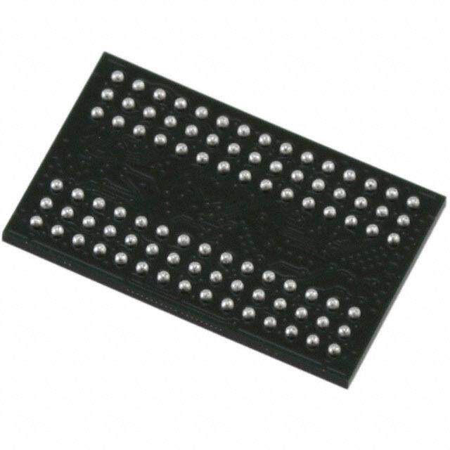
| 描述 | IC SRAM 36MBIT 600MHZ 165FBGA |
| 产品分类 | |
| 品牌 | Cypress Semiconductor Corp |
| 数据手册 | http://www.cypress.com/?docID=50153 |
| 产品图片 |
|
| 产品型号 | CY7C1270XV18-600BZXC |
| rohs | 无铅 / 符合限制有害物质指令(RoHS)规范要求 |
| 产品系列 | - |
| 供应商器件封装 | 165-FBGA(13x15) |
| 其它名称 | CY7C1270XV18600BZXC |
| 包装 | 托盘 |
| 存储器类型 | SRAM - 同步,DDR II |
| 存储容量 | 36M(1M x 36) |
| 封装/外壳 | 165-LBGA |
| 工作温度 | 0°C ~ 70°C |
| 接口 | 并联 |
| 标准包装 | 136 |
| 格式-存储器 | RAM |
| 电压-电源 | 1.7 V ~ 1.9 V |
| 速度 | 600MHz |


_renders/IS45S16320F-7BLA1.jpg)


_renders/IS42S32800D-6BLI.jpg)


- 商务部:美国ITC正式对集成电路等产品启动337调查
- 曝三星4nm工艺存在良率问题 高通将骁龙8 Gen1或转产台积电
- 太阳诱电将投资9.5亿元在常州建新厂生产MLCC 预计2023年完工
- 英特尔发布欧洲新工厂建设计划 深化IDM 2.0 战略
- 台积电先进制程称霸业界 有大客户加持明年业绩稳了
- 达到5530亿美元!SIA预计今年全球半导体销售额将创下新高
- 英特尔拟将自动驾驶子公司Mobileye上市 估值或超500亿美元
- 三星加码芯片和SET,合并消费电子和移动部门,撤换高东真等 CEO
- 三星电子宣布重大人事变动 还合并消费电子和移动部门
- 海关总署:前11个月进口集成电路产品价值2.52万亿元 增长14.8%


PDF Datasheet 数据手册内容提取
Please note that Cypress is an Infineon Technologies Company. The document following this cover page is marked as “Cypress” document as this is the company that originally developed the product. Please note that Infineon will continue to offer the product to new and existing customers as part of the Infineon product portfolio. Continuity of document content The fact that Infineon offers the following product as part of the Infineon product portfolio does not lead to any changes to this document. Future revisions will occur when appropriate, and any changes will be set out on the document history page. Continuity of ordering part numbers Infineon continues to support existing part numbers. Please continue to use the ordering part numbers listed in the datasheet for ordering. www.infineon.com
CY7C1268XV18 CY7C1270XV18 36-Mbit DDR II+ Xtreme SRAM Two-Word Burst Architecture (2.5 Cycle Read Latency) 36-Mbit DDR II+ Xtreme SRAM Two-Word Burst Architecture (2.5 Cycle Read Latency) Features Configurations ■36-Mbit density (2 M × 18, 1 M × 36) With Read Cycle Latency of 2.5 cycles: ■633 MHz clock for high bandwidth CY7C1268XV18 – 2 M × 18 CY7C1270XV18 – 1 M × 36 ■Two-word burst for reducing address bus frequency ■Double data rate (DDR) interfaces (data transferred at Functional Description 1266MHz) at 633 MHz The CY7C1268XV18, and CY7C1270XV18 are 1.8V ■Available in 2.5 clock cycle latency synchronous pipelined SRAMs equipped with DDR II+ ■Two input clocks (K and K) for precise DDR timing architecture. The DDR II+ consists of an SRAM core with advanced synchronous peripheral circuitry. Addresses for read ❐SRAM uses rising edges only and write are latched on alternate rising edges of the input (K) ■Echo clocks (CQ and CQ) simplify data capture in high speed clock. Write data is registered on the rising edges of both K and systems K. Read data is driven on the rising edges of K and K. Each address location is associated with two 18-bit words ■Data valid pin (QVLD) to indicate valid data on the output (CY7C1268XV18), or 36-bit words (CY7C1270XV18) that burst ■Synchronous internally self-timed writes sequentially into or out of the device. Asynchronous inputs include an output impedance matching ■DDR II+ Xtreme operates with 2.5 cycle read latency when input (ZQ). Synchronous data outputs (Q, sharing the same DOFF is asserted HIGH physical pins as the data inputs D) are tightly matched to the two ■Operates similar to DDR I device with 1 cycle read latency when output echo clocks CQ/CQ, eliminating the need for separately DOFF is asserted LOW capturing data from each individual DDR SRAM in the system design. ■Core V = 1.8 V ± 0.1 V; I/O V = 1.4 V to 1.6 V DD DDQ All synchronous inputs pass through input registers controlled by ❐Supports 1.5 V I/O supply the K or K input clocks. All data outputs pass through output ■HSTL inputs and variable drive HSTL output buffers registers controlled by the K or K input clocks. Writes are ■Available in 165-ball fine pitch ball grid array (FBGA) package conducted with on-chip synchronous self-timed write circuitry. (13 × 15 × 1.4 mm) For a complete list of related documentation, click here. ■Offered in Pb-free packages ■JTAG 1149.1 compatible test access port ■Phase-locked loop (PLL) for accurate data placement Selection Guide Description 633 MHz 600 MHz Unit Maximum operating frequency 633 600 MHz Maximum operating current × 18 965 910 mA × 36 1230 1165 CypressSemiconductorCorporation • 198 Champion Court • SanJose, CA 95134-1709 • 408-943-2600 Document Number: 001-70329 Rev. *F Revised December 15, 2017
CY7C1268XV18 CY7C1270XV18 Logic Block Diagram – CY7C1268XV18 Write Write 20 A(19:0) Reg Reg Address LD Register code 1M 1M code 18 De x x De d. 18 18 d. KK GCLeKn. Write Ad Array Array Read Ad OCLouontgptirucotl R/W DOFF Read Data Reg. 36 CQ VREF 18 18 Control Reg. Reg. CQ R/W Logic BWS[1:0] 18 Reg. 18 18 DQ [17:0] QVLD Logic Block Diagram – CY7C1270XV18 Write Write 19 A(18:0) Reg Reg Address LD Register code 512 512 code 36 e K K e d. D x 3 x 3 d. D K d 6 6 d K GCLeKn. Write A Array Array Read A OCLouontgptirucotl R/W DOFF Read Data Reg. 72 CQ VREF 36 36 Control Reg. Reg. CQ R/W Logic BWS[3:0] 36 Reg. 36 36 DQ [35:0] QVLD Document Number: 001-70329 Rev. *F Page 2 of 28
CY7C1268XV18 CY7C1270XV18 Contents Pin Configurations ...........................................................4 Boundary Scan Order ....................................................17 Pin Definitions ..................................................................5 Power Up Sequence in DDR II+ Xtreme SRAM ............18 Functional Overview ........................................................6 Power Up Sequence .................................................18 Read Operations .........................................................6 PLL Constraints .........................................................18 Write Operations .........................................................6 Maximum Ratings ...........................................................19 Byte Write Operations .................................................6 Operating Range .............................................................19 DDR Operation ............................................................7 Neutron Soft Error Immunity .........................................19 Depth Expansion .........................................................7 Electrical Characteristics ...............................................19 Programmable Impedance ..........................................7 DC Electrical Characteristics .....................................19 Echo Clocks ................................................................7 AC Electrical Characteristics .....................................20 Valid Data Indicator (QVLD) ........................................7 Capacitance ....................................................................20 PLL ..............................................................................7 Thermal Resistance ........................................................20 Application Example ........................................................7 AC Test Loads and Waveforms .....................................21 Truth Table ........................................................................8 Switching Characteristics ..............................................22 Write Cycle Descriptions .................................................8 Switching Waveforms ....................................................23 Write Cycle Descriptions .................................................9 Read/Write/Deselect Sequence ................................23 IEEE 1149.1 Serial Boundary Scan (JTAG) ..................10 Ordering Information ......................................................24 Disabling the JTAG Feature ......................................10 Ordering Code Definitions .........................................24 Test Access Port .......................................................10 Package Diagram ............................................................25 Performing a TAP Reset ...........................................10 Acronyms ........................................................................26 TAP Registers ...........................................................10 Document Conventions .................................................26 TAP Instruction Set ...................................................10 Units of Measure .......................................................26 TAP Controller State Diagram .......................................12 Document History Page .................................................27 TAP Controller Block Diagram ......................................13 Sales, Solutions, and Legal Information ......................28 TAP Electrical Characteristics ......................................13 Worldwide Sales and Design Support .......................28 TAP AC Switching Characteristics ...............................14 Products ....................................................................28 TAP Timing and Test Conditions ..................................15 PSoC® Solutions ......................................................28 Identification Register Definitions ................................16 Cypress Developer Community .................................28 Scan Register Sizes .......................................................16 Technical Support .....................................................28 Instruction Codes ...........................................................16 Document Number: 001-70329 Rev. *F Page 3 of 28
CY7C1268XV18 CY7C1270XV18 Pin Configurations The pin configurations for CY7C1268XV18, and CY7C1270XV18 follow. [1] Figure 1. 165-ball FBGA (13 × 15 × 1.4 mm) pinout CY7C1268XV18 (2 M × 18) 1 2 3 4 5 6 7 8 9 10 11 A CQ NC/72M A R/W BWS K NC/144M LD A A CQ 1 B NC DQ9 NC A NC/288M K BWS A NC NC DQ8 0 C NC NC NC V A NC A V NC DQ7 NC SS SS D NC NC DQ10 V V V V V NC NC NC SS SS SS SS SS E NC NC DQ11 V V V V V NC NC DQ6 DDQ SS SS SS DDQ F NC DQ12 NC V V V V V NC NC DQ5 DDQ DD SS DD DDQ G NC NC DQ13 V V V V V NC NC NC DDQ DD SS DD DDQ H DOFF V V V V V V V V V ZQ REF DDQ DDQ DD SS DD DDQ DDQ REF J NC NC NC V V V V V NC DQ4 NC DDQ DD SS DD DDQ K NC NC DQ14 V V V V V NC NC DQ3 DDQ DD SS DD DDQ L NC DQ15 NC V V V V V NC NC DQ2 DDQ SS SS SS DDQ M NC NC NC V V V V V NC DQ1 NC SS SS SS SS SS N NC NC DQ16 V A A A V NC NC NC SS SS P NC NC DQ17 A A QVLD A A NC NC DQ0 R TDO TCK A A A NC A A A TMS TDI CY7C1270XV18 (1 M × 36) 1 2 3 4 5 6 7 8 9 10 11 A CQ NC/144M A R/W BWS K BWS LD A NC/72M CQ 2 1 B NC DQ27 DQ18 A BWS K BWS A NC NC DQ8 3 0 C NC NC DQ28 V A NC A V NC DQ17 DQ7 SS SS D NC DQ29 DQ19 V V V V V NC NC DQ16 SS SS SS SS SS E NC NC DQ20 V V V V V NC DQ15 DQ6 DDQ SS SS SS DDQ F NC DQ30 DQ21 V V V V V NC NC DQ5 DDQ DD SS DD DDQ G NC DQ31 DQ22 V V V V V NC NC DQ14 DDQ DD SS DD DDQ H DOFF V V V V V V V V V ZQ REF DDQ DDQ DD SS DD DDQ DDQ REF J NC NC DQ32 V V V V V NC DQ13 DQ4 DDQ DD SS DD DDQ K NC NC DQ23 V V V V V NC DQ12 DQ3 DDQ DD SS DD DDQ L NC DQ33 DQ24 V V V V V NC NC DQ2 DDQ SS SS SS DDQ M NC NC DQ34 V V V V V NC DQ11 DQ1 SS SS SS SS SS N NC DQ35 DQ25 V A A A V NC NC DQ10 SS SS P NC NC DQ26 A A QVLD A A NC DQ9 DQ0 R TDO TCK A A A NC A A A TMS TDI Note 1. NC/72M, NC/144M and NC/288M are not connected to the die and can be tied to any voltage level. Document Number: 001-70329 Rev. *F Page 4 of 28
CY7C1268XV18 CY7C1270XV18 Pin Definitions Pin Name I/O Pin Description DQ Input Output- Data input output signals. Inputs are sampled on the rising edge of K and K clocks during valid write [x:0] Synchronous operations. These pins drive out the requested data when the read operation is active. Valid data is driven out on the rising edge of both the K and K clocks during read operations. When read access is deselected, Q are automatically tristated. [x:0] CY7C1268XV18 DQ [17:0] CY7C1270XV18 DQ [35:0] LD Input- Synchronous load. Sampled on the rising edge of the K clock. This input is brought LOW when a bus Synchronous cycle sequence is defined. This definition includes address and read/write direction. All transactions operate on a burst of 2 data. LD must meet the setup and hold times around edge of K. BWS , Input- Byte Write Select 0, 1, 2 and 3 Active LOW. Sampled on the rising edge of the K and K clocks during 0 BWS , Synchronous write operations. Used to select which byte is written into the device during the current portion of the 1 BWS , write operations. Bytes not written remain unaltered. 2 BWS CY7C1268XV18 BWS controls D and BWS controls D 3 0 [8:0] 1 [17:9]. CY7C1270XV18 BWS controls D , BWS controls D , BWS controls D and BWS 0 [8:0] 1 [17:9] 2 [26:18] 3 controls D . [35:27] All the Byte Write Selects are sampled on the same edge as the data. Deselecting a Byte Write Select ignores the corresponding byte of data and it is not written into the device. A Input- Address inputs. Sampled on the rising edge of the K clock during active read and write operations. Synchronous These address inputs are multiplexed for both read and write operations. Internally, the device is organized as 2 M × 18 (2 arrays each of 1 M × 18) for CY7C1268XV18, and 1 M × 36 (2 arrays each of 512 K × 36) for CY7C1270XV18. The address pins (A) can be assigned any bit order. R/W Input- Synchronous read or write input. When LD is LOW, this input designates the access type (read when Synchronous R/W is HIGH, write when R/W is LOW) for loaded address. R/W must meet the setup and hold times around edge of K. QVLD Valid output Valid output indicator. The Q Valid indicates valid output data. QVLD is edge aligned with CQ and CQ. indicator K Input Clock Positive input clock input. The rising edge of K is used to capture synchronous inputs to the device and to drive out data through Q . All accesses are initiated on the rising edge of K. [x:0] K Input Clock Negative input clock input. K is used to capture synchronous data being presented to the device and to drive out data through Q . [x:0] CQ Echo Clock Synchronous echo clock outputs. This is a free running clock and is synchronized to the input clock (K) of the DDR II+ Xtreme. The timing for the echo clocks is shown in the Switching Characteristics on page 22. CQ Echo Clock Synchronous echo clock outputs. This is a free running clock and is synchronized to the input clock (K) of the DDR II+ Xtreme. The timing for the echo clocks is shown in the Switching Characteristics on page 22. ZQ Input Output impedance matching input. This input is used to tune the device outputs to the system data bus impedance. CQ, CQ, and Q output impedance are set to 0.2 × RQ, where RQ is a resistor [x:0] connected between ZQ and ground. Alternatively, this pin can be connected directly to V , which DDQ enables the minimum impedance mode. This pin cannot be connected directly to GND or left unconnected. DOFF Input PLL Turn Off Active LOW. Connecting this pin to ground turns off the PLL inside the device. The timing in the PLL turned off operation differs from those listed in this data sheet. For normal operation, this pin can be connected to a pull up through a 10 k or less pull up resistor. The device behaves in DDR I mode when the PLL is turned off. In this mode, the device can be operated at a frequency of up to 167MHz with DDR I timing. Document Number: 001-70329 Rev. *F Page 5 of 28
CY7C1268XV18 CY7C1270XV18 Pin Definitions (continued) Pin Name I/O Pin Description TDO Output Test data out (TDO) pin for JTAG. TCK Input Test clock (TCK) pin for JTAG. TDI Input Test data in (TDI) pin for JTAG. TMS Input Test mode select (TMS) pin for JTAG. NC N/A Not connected to the die. Can be tied to any voltage level. NC/72M Input Not connected to the die. Can be tied to any voltage level. NC/144M Input Not connected to the die. Can be tied to any voltage level. NC/288M Input Not connected to the die. Can be tied to any voltage level. V Input- Reference voltage input. Static input used to set the reference level for HSTL inputs, outputs, and AC REF Reference measurement points. V Power Supply Power supply inputs to the core of the device. DD V Ground Ground for the device. SS V Power Supply Power supply inputs for the outputs of the device. DDQ Functional Overview When read access is deselected, the CY7C1268XV18 first completes the pending read transactions. Synchronous internal The CY7C1268XV18, and CY7C1270XV18 are synchronous circuitry automatically tristates the output following the next rising pipelined Burst SRAMs equipped with a DDR interface, which edge of the negative input clock (K). This enables for a transition operates with a read latency of two and half cycles when DOFF between devices without the insertion of wait states in a depth pin is tied HIGH. When DOFF pin is set LOW or connected to expanded memory. V the device behaves in DDR I mode with a read latency of SS Write Operations one clock cycle. Accesses are initiated on the rising edge of the positive input Write operations are initiated by asserting R/W LOW and LD clock (K). All synchronous input and output timing is referenced LOW at the rising edge of the positive input clock (K). The from the rising edge of the input clocks (K and K). address presented to address inputs is stored in the write address register. On the following K clock rise, the data All synchronous data inputs (D ) pass through input registers [x:0] presented to D is latched and stored into the 18-bit write controlled by the rising edge of the input clocks (K and K). All [17:0] data register, provided BWS are both asserted active. On the synchronous data outputs (Q ) pass through output registers [1:0] [x:0] subsequent rising edge of the negative input clock (K) the controlled by the rising edge of the input clocks (K and K). information presented to D is also stored into the write data [17:0] All synchronous control (R/W, LD, BWS ) inputs pass through register, provided BWS are both asserted active. The 36 bits [X:0] [1:0] input registers controlled by the rising edge of the input clock (K). of data are then written into the memory array at the specified location. Write accesses can be initiated on every rising edge of CY7C1268XV18 is described in the following sections. The the positive input clock (K). Doing so pipelines the data flow such same basic descriptions apply to CY7C1270XV18. that 18 bits of data can be transferred into the device on every Read Operations rising edge of the input clocks (K and K). The CY7C1268XV18 is organized internally as two arrays of When the write access is deselected, the device ignores all 1M×18. Accesses are completed in a burst of 2 sequential inputs after the pending write operations have been completed. 18-bit data words. Read operations are initiated by asserting Byte Write Operations R/WHIGH and LD LOW at the rising edge of the positive input clock (K). The address presented to the address inputs is stored Byte write operations are supported by the CY7C1268XV18. A in the read address register. Following the next two K clock rise, write operation is initiated as described in the Write Operations the corresponding 18-bit word of data from this address location section. The bytes that are written are determined by BWS and 0 is driven onto the Q using K as the output timing reference. BWS , which are sampled with each set of 18-bit data words. [17:0] 1 On the subsequent rising edge of K, the next 18-bit data word is Asserting the appropriate Byte Write Select input during the data driven onto the Q . The requested data is valid 0.45 ns from portion of a write latches the data being presented and writes it [17:0] the rising edge of the input clock (K and K). To maintain the into the device. Deasserting the Byte Write Select input during internal logic, each read access must be allowed to complete. the data portion of a write enables the data stored in the device Read accesses can be initiated on every rising edge of the for that byte to remain unaltered. This feature can be used to positive input clock (K). simplify read, modify, or write operations to a byte write operation. Document Number: 001-70329 Rev. *F Page 6 of 28
CY7C1268XV18 CY7C1270XV18 DDR Operation output impedance is adjusted every 1024 cycles upon power up to account for drifts in supply voltage and temperature. The CY7C1268XV18 enables high-performance operation through high clock frequencies (achieved through pipelining) and Echo Clocks DDR mode of operation. The CY7C1268XV18 requires two No Operation (NOP) cycle during transition from a read to a write Echo clocks are provided on the DDR II+ Xtreme to simplify data cycle. At higher frequencies, some applications require third capture on high-speed systems. Two echo clocks are generated NOP cycle to avoid contention. by the DDR II+ Xtreme. CQ is referenced with respect to K and CQ is referenced with respect to K. These are free-running If a read occurs after a write cycle, address and data for the write clocks and are synchronized to the input clock of the DDR II+ are stored in registers. The write information is stored because Xtreme. The timing for the echo clocks is shown in the Switching the SRAM cannot perform the last word write to the array without Characteristics on page 22. conflicting with the read. The data stays in this register until the next write cycle occurs. On the first write cycle after the read(s), Valid Data Indicator (QVLD) the stored data from the earlier write is written into the SRAM array. This is called a Posted write. QVLD is provided on the DDR II+ Xtreme to simplify data capture on high speed systems. The QVLD is generated by the DDR II+ If a read is performed on the same address on which a write is Xtreme device along with data output. This signal is also edge performed in the previous cycle, the SRAM reads out the most aligned with the echo clock and follows the timing of any data pin. current data. The SRAM does this by bypassing the memory This signal is asserted half a cycle before valid data arrives. array and reading the data from the registers. PLL Depth Expansion These chips use a PLL that is designed to function between Depth expansion requires replicating the LD control signal for 120MHz and the specified maximum clock frequency. During each bank. All other control signals can be common between power up, when the DOFF is tied HIGH, the PLL is locked after banks as appropriate. 100 s of stable clock. The PLL can also be reset by slowing or stopping the input clock K and K for a minimum of 30 ns. Programmable Impedance However, it is not necessary to reset the PLL to lock to the An external resistor, RQ, must be connected between the ZQ pin desired frequency. The PLL automatically locks 100 s after a on the SRAM and V to allow the SRAM to adjust its output stable clock is presented. The PLL may be disabled by applying SS driver impedance. The value of RQ must be 5 × the value of the ground to the DOFF pin. When the PLL is turned off, the device intended line impedance driven by the SRAM. The allowable behaves in DDR I mode (with one cycle latency and a longer range of RQ to guarantee impedance matching with a tolerance access time). For information, refer to the application note, PLL of ±15% is between 175 and 350 , with VDDQ=1.5 V. The Considerations in QDRII/DDRII/QDRII+/DDRII+. Application Example Figure2 shows two DDR II+ Xtreme used in an application. Figure 2. Application Example (Width Expansion) ZQ ZQ SRAM#1 SRAM#2 CQ/CQ CQ/CQ RQ RQ DQ[x:0] DQ[x:0] A LD R/W BWS K K A LD R/W BWS K K DQ[2x:0] ADDRESS LD R/W BWS CLKIN1/CLKIN1 CLKIN2/CLKIN2 SOURCE K SOURCE K FPGA / ASIC Document Number: 001-70329 Rev. *F Page 7 of 28
CY7C1268XV18 CY7C1270XV18 Truth Table The truth table for the CY7C1268XV18, and CY7C1270XV18 follows. [2, 3, 4, 5, 6, 7] Operation K LD R/W DQ DQ Write cycle: L–H L L D(A) at K(t + 1) D(A+1) at K(t + 1) Load address; wait one cycle; input write data on consecutive K and K rising edges. Read cycle: (2.5 cycle Latency) L–H L H Q(A) at K(t + 2) Q(A+1) at K(t + 3) Load address; wait two and half cycles; read data on consecutive K and K rising edges. NOP: No operation L–H H X High Z High Z Standby: Clock stopped Stopped X X Previous State Previous State Write Cycle Descriptions The write cycle description table for CY7C1268XV18 follows. [2, 8] BWS0 BWS1 K K Comments L L L–H – During the data portion of a write sequence CY7C1268XV18 both bytes (D ) are written into the device. [17:0] L L – L–H During the data portion of a write sequence: CY7C1268XV18 both bytes (D ) are written into the device. [17:0] L H L–H – During the data portion of a write sequence: CY7C1268XV18 only the lower byte (D ) is written into the device, D remains unaltered. [8:0] [17:9] L H – L–H During the data portion of a write sequence CY7C1268XV18 only the lower byte (D ) is written into the device, D remains unaltered. [8:0] [17:9] H L L–H – During the data portion of a write sequence CY7C1268XV18 only the upper byte (D ) is written into the device, D remains unaltered. [17:9] [8:0] H L – L–H During the data portion of a write sequence CY7C1268XV18 only the upper byte (D ) is written into the device, D remains unaltered. [17:9] [8:0] H H L–H – No data is written into the devices during this portion of a write operation. H H – L–H No data is written into the devices during this portion of a write operation. Notes 2. X = “Don’t Care,” H = Logic HIGH, L = Logic LOW, represents rising edge. 3. Device powers up deselected with the outputs in a tristate condition. 4. “A” represents address location latched by the devices when transaction was initiated. A + 1 represents the address sequence in the burst. 5. “t” represents the cycle at which a read/write operation is started. t + 1 and t + 2 are the first and second clock cycles succeeding the “t” clock cycle. 6. Data inputs are registered at K and K rising edges. Data outputs are delivered on K and K rising edges as well. 7. Ensure that when clock is stopped K = K. This is not essential, but permits most rapid restart by overcoming transmission line charging symmetrically. 8. Is based on a write cycle that was initiated in accordance with the Truth Table. BWS0, BWS1, BWS2, and BWS3 can be altered on different portions of a write cycle, as long as the setup and hold requirements are achieved. Document Number: 001-70329 Rev. *F Page 8 of 28
CY7C1268XV18 CY7C1270XV18 Write Cycle Descriptions The write cycle description table for CY7C1270XV18 follows. [9, 10] BWS BWS BWS BWS K K Comments 0 1 2 3 L L L L L–H – During the data portion of a write sequence, all four bytes (D ) are written into [35:0] the device. L L L L – L–H During the data portion of a write sequence, all four bytes (D ) are written into [35:0] the device. L H H H L–H – During the data portion of a write sequence, only the lower byte (D ) is written [8:0] into the device. D remains unaltered. [35:9] L H H H – L–H During the data portion of a write sequence, only the lower byte (D ) is written [8:0] into the device. D remains unaltered. [35:9] H L H H L–H – During the data portion of a write sequence, only the byte (D ) is written into the [17:9] device. D and D remains unaltered. [8:0] [35:18] H L H H – L–H During the data portion of a write sequence, only the byte (D ) is written into the [17:9] device. D and D remains unaltered. [8:0] [35:18] H H L H L–H – During the data portion of a write sequence, only the byte (D ) is written into [26:18] the device. D and D remains unaltered. [17:0] [35:27] H H L H – L–H During the data portion of a write sequence, only the byte (D ) is written into [26:18] the device. D and D remains unaltered. [17:0] [35:27] H H H L L–H – During the data portion of a write sequence, only the byte (D ) is written into [35:27] the device. D remains unaltered. [26:0] H H H L – L–H During the data portion of a write sequence, only the byte (D ) is written into [35:27] the device. D remains unaltered. [26:0] H H H H L–H – No data is written into the device during this portion of a write operation. H H H H – L–H No data is written into the device during this portion of a write operation. Notes 9. X = “Don’t Care,” H = Logic HIGH, L = Logic LOW, represents rising edge. 10.Is based on a write cycle that was initiated in accordance with the Truth Table on page 8. BWS0, BWS1, BWS2, and BWS3 can be altered on different portions of a write cycle, as long as the setup and hold requirements are achieved. Document Number: 001-70329 Rev. *F Page 9 of 28
CY7C1268XV18 CY7C1270XV18 IEEE 1149.1 Serial Boundary Scan (JTAG) Instruction Register Three-bit instructions can be serially loaded into the instruction These SRAMs incorporate a serial boundary scan Test Access register. This register is loaded when it is placed between the TDI Port (TAP) in the FBGA package. This part is fully compliant with and TDO pins, as shown in TAP Controller Block Diagram on IEEE Standard #1149.1-2001. The TAP operates using JEDEC page 13. Upon power up, the instruction register is loaded with standard 1.8V I/O logic levels. the IDCODE instruction. It is also loaded with the IDCODE instruction if the controller is placed in a reset state, as described Disabling the JTAG Feature in the previous section. It is possible to operate the SRAM without using the JTAG When the TAP controller is in the Capture-IR state, the two least feature. To disable the TAP controller, TCK must be tied LOW significant bits are loaded with a binary “01” pattern to allow for (V ) to prevent clocking of the device. TDI and TMS are SS fault isolation of the board level serial test path. internally pulled up and may be unconnected. They may alternatively be connected to VDD through a pull up resistor. TDO Bypass Register must be left unconnected. Upon power up, the device comes up To save time when serially shifting data through registers, it is in a reset state, which does not interfere with the operation of the sometimes advantageous to skip certain chips. The bypass device. register is a single-bit register that can be placed between TDI Test Access Port and TDO pins. This enables shifting of data through the SRAM with minimal delay. The bypass register is set LOW (V ) when SS Test Clock the BYPASS instruction is executed. The test clock is used only with the TAP controller. All inputs are Boundary Scan Register captured on the rising edge of TCK. All outputs are driven from the falling edge of TCK. The boundary scan register is connected to all of the input and output pins on the SRAM. Several No Connect (NC) pins are also Test Mode Select (TMS) included in the scan register to reserve pins for higher density devices. The TMS input is used to give commands to the TAP controller and is sampled on the rising edge of TCK. This pin may be left The boundary scan register is loaded with the contents of the unconnected if the TAP is not used. The pin is pulled up RAM input and output ring when the TAP controller is in the internally, resulting in a logic HIGH level. Capture-DR state and is then placed between the TDI and TDO pins when the controller is moved to the Shift-DR state. The Test Data-In (TDI) EXTEST, SAMPLE/PRELOAD, and SAMPLE Z instructions can be used to capture the contents of the input and output ring. The TDI pin is used to serially input information into the registers and can be connected to the input of any of the registers. The The Boundary Scan Order on page 17 shows the order in which register between TDI and TDO is chosen by the instruction that the bits are connected. Each bit corresponds to one of the bumps is loaded into the TAP instruction register. For information about on the SRAM package. The MSB of the register is connected to loading the instruction register, see the TAP Controller State TDI, and the LSB is connected to TDO. Diagram on page 12. TDI is internally pulled up and can be unconnected if the TAP is unused in an application. TDI is Identification (ID) Register connected to the most significant bit (MSB) on any register. The ID register is loaded with a vendor-specific, 32-bit code during the Capture-DR state when the IDCODE command is Test Data-Out (TDO) loaded in the instruction register. The IDCODE is hardwired into The TDO output pin is used to serially clock data out from the the SRAM and can be shifted out when the TAP controller is in registers. The output is active, depending upon the current state the Shift-DR state. The ID register has a vendor code and other of the TAP state machine (see Instruction Codes on page 16). information described in Identification Register Definitions on The output changes on the falling edge of TCK. TDO is page 16. connected to the least significant bit (LSB) of any register. TAP Instruction Set Performing a TAP Reset Eight different instructions are possible with the three-bit A Reset is performed by forcing TMS HIGH (VDD) for five rising instruction register. All combinations are listed in Instruction edges of TCK. This Reset does not affect the operation of the Codes on page 16. Three of these instructions are listed as SRAM and can be performed while the SRAM is operating. At RESERVED and must not be used. The other five instructions power up, the TAP is reset internally to ensure that TDO comes are described in this section in detail. up in a High Z state. Instructions are loaded into the TAP controller during the Shift-IR TAP Registers state when the instruction register is placed between TDI and TDO. During this state, instructions are shifted through the Registers are connected between the TDI and TDO pins to scan instruction register through the TDI and TDO pins. To execute the data in and out of the SRAM test circuitry. Only one register the instruction after it is shifted in, the TAP controller must be can be selected at a time through the instruction registers. Data moved into the Update-IR state. is serially loaded into the TDI pin on the rising edge of TCK. Data is output on the TDO pin on the falling edge of TCK. Document Number: 001-70329 Rev. *F Page 10 of 28
CY7C1268XV18 CY7C1270XV18 IDCODE PRELOAD places an initial data pattern at the latched parallel outputs of the boundary scan register cells before the selection The IDCODE instruction loads a vendor-specific, 32-bit code into of another boundary scan test operation. the instruction register. It also places the instruction register between the TDI and TDO pins and shifts the IDCODE out of the The shifting of data for the SAMPLE and PRELOAD phases can device when the TAP controller enters the Shift-DR state. The occur concurrently when required, that is, while the data IDCODE instruction is loaded into the instruction register at captured is shifted out, the preloaded data can be shifted in. power up or whenever the TAP controller is supplied a Test-Logic-Reset state. BYPASS When the BYPASS instruction is loaded in the instruction register SAMPLE Z and the TAP is placed in a Shift-DR state, the bypass register is The SAMPLE Z instruction connects the boundary scan register placed between the TDI and TDO pins. The advantage of the between the TDI and TDO pins when the TAP controller is in a BYPASS instruction is that it shortens the boundary scan path Shift-DR state. The SAMPLE Z command puts the output bus when multiple devices are connected together on a board. into a High Z state until the next command is supplied during the Update IR state. EXTEST The EXTEST instruction drives the preloaded data out through SAMPLE/PRELOAD the system output pins. This instruction also connects the SAMPLE/PRELOAD is a 1149.1 mandatory instruction. When boundary scan register for serial access between the TDI and the SAMPLE/PRELOAD instructions are loaded into the TDO in the Shift-DR controller state. instruction register and the TAP controller is in the Capture-DR state, a snapshot of data on the input and output pins is captured EXTEST OUTPUT BUS TRISTATE in the boundary scan register. IEEE Standard 1149.1 mandates that the TAP controller be able The user must be aware that the TAP controller clock can only to put the output bus into a tristate mode. operate at a frequency up to 20 MHz, while the SRAM clock The boundary scan register has a special bit located at bit #108. operates more than an order of magnitude faster. Because there When this scan cell, called the “extest output bus tristate,” is is a large difference in the clock frequencies, it is possible that latched into the preload register during the Update-DR state in during the Capture-DR state, an input or output undergoes a the TAP controller, it directly controls the state of the output transition. The TAP may then try to capture a signal while in (Q-bus) pins, when the EXTEST is entered as the current transition (metastable state). This does not harm the device, but instruction. When HIGH, it enables the output buffers to drive the there is no guarantee as to the value that is captured. output bus. When LOW, this bit places the output bus into a Repeatable results may not be possible. HighZ condition. To guarantee that the boundary scan register captures the This bit can be set by entering the SAMPLE/PRELOAD or correct value of a signal, the SRAM signal must be stabilized EXTEST command, and then shifting the desired bit into that cell, long enough to meet the TAP controller’s capture setup plus hold during the Shift-DR state. During Update-DR, the value loaded times (tCS and tCH). The SRAM clock input might not be captured into that shift-register cell latches into the preload register. When correctly if there is no way in a design to stop (or slow) the clock the EXTEST instruction is entered, this bit directly controls the during a SAMPLE/PRELOAD instruction. If this is an issue, it is output Q-bus pins. Note that this bit is preset HIGH to enable the still possible to capture all other signals and simply ignore the output when the device is powered up, and also when the TAP value of the CK and CK captured in the boundary scan register. controller is in the Test-Logic-Reset state. After the data is captured, it is possible to shift out the data by Reserved putting the TAP into the Shift-DR state. This places the boundary scan register between the TDI and TDO pins. These instructions are not implemented but are reserved for future use. Do not use these instructions. Document Number: 001-70329 Rev. *F Page 11 of 28
CY7C1268XV18 CY7C1270XV18 TAP Controller State Diagram The state diagram for the TAP controller follows. [11] TEST-LOGIC 1 RESET 0 1 TEST-LOGIC/ 1 SELECT 1 SELECT 0 IDLE DR-SCAN IR-SCAN 0 0 1 1 CAPTURE-DR CAPTURE-IR 0 0 SHIFT-DR 0 SHIFT-IR 0 1 1 1 1 EXIT1-DR EXIT1-IR 0 0 PAUSE-DR 0 PAUSE-IR 0 1 1 0 0 EXIT2-DR EXIT2-IR 1 1 UPDATE-DR UPDATE-IR 1 1 0 0 Note 11.The 0/1 next to each state represents the value at TMS at the rising edge of TCK. Document Number: 001-70329 Rev. *F Page 12 of 28
CY7C1268XV18 CY7C1270XV18 TAP Controller Block Diagram 0 Bypass Register 2 1 0 TDI Selection Instruction Register Selection TDO Circuitry Circuitry 31 30 29 . . 2 1 0 Identification Register 108 . . . . 2 1 0 Boundary Scan Register TCK TAP Controller TMS TAP Electrical Characteristics Over the Operating Range Parameter [12, 13, 14] Description Test Conditions Min Max Unit V Output HIGH voltage I =2.0 mA 1.4 – V OH1 OH V Output HIGH voltage I =100 A 1.6 – V OH2 OH V Output LOW voltage I = 2.0 mA – 0.4 V OL1 OL V Output LOW voltage I = 100 A – 0.2 V OL2 OL V Input HIGH voltage – 0.65 × V V + 0.3 V IH DD DD V Input LOW voltage – –0.3 0.35 × V V IL DD I Input and output load current GND V V –5 5 A X I DD Notes 12.These characteristics pertain to the TAP inputs (TMS, TCK, TDI and TDO). Parallel load levels are specified in the Electrical Characteristics on page 19. 13.Overshoot: VIH(AC) < VDD + 0.3 V (Pulse width less than tTCYC/2), Undershoot: VIL(AC) > 0.3 V (Pulse width less than tTCYC/2). 14.All Voltage referenced to Ground. Document Number: 001-70329 Rev. *F Page 13 of 28
CY7C1268XV18 CY7C1270XV18 TAP AC Switching Characteristics Over the Operating Range Parameter [15, 16] Description Min Max Unit t TCK clock cycle time 50 – ns TCYC t TCK clock frequency – 20 MHz TF t TCK clock HIGH 20 – ns TH t TCK clock LOW 20 – ns TL Setup Times t TMS setup to TCK clock rise 5 – ns TMSS t TDI setup to TCK clock rise 5 – ns TDIS t Capture setup to TCK rise 5 – ns CS Hold Times t TMS hold after TCK clock rise 5 – ns TMSH t TDI hold after clock rise 5 – ns TDIH t Capture hold after clock rise 5 – ns CH Output Times t TCK clock LOW to TDO valid – 10 ns TDOV t TCK clock LOW to TDO invalid 0 – ns TDOX Notes 15.tCS and tCH refer to the setup and hold time requirements of latching data from the boundary scan register. 16.Test conditions are specified using the load in TAP AC Test Conditions. tR/tF = 1 V/ns. Document Number: 001-70329 Rev. *F Page 14 of 28
CY7C1268XV18 CY7C1270XV18 TAP Timing and Test Conditions Figure3 shows the TAP timing and test conditions. [17] Figure 3. TAP Timing and Test Conditions 0.9 V ALL INPUT PULSES 1.8 V 50 0.9 V TDO 0 V Slew Rate = 1 V/ns Z0= 50 CL= 20 pF (a) GND tTH tTL Test Clock TCK t TCYC t TMSH t TMSS Test Mode Select TMS t TDIS t TDIH Test Data In TDI Test Data Out TDO tTDOV tTDOX Note 17.Test conditions are specified using the load in TAP AC Test Conditions. tR/tF = 1 V/ns. Document Number: 001-70329 Rev. *F Page 15 of 28
CY7C1268XV18 CY7C1270XV18 Identification Register Definitions Value Instruction Field Description CY7C1268XV18 CY7C1270XV18 Revision number (31:29) 000 000 Version number. Cypress device ID (28:12) 11010111000010100 11010111000100100 Defines the type of SRAM. Cypress JEDEC ID (11:1) 00000110100 00000110100 Allows unique identification of SRAM vendor. ID register presence (0) 1 1 Indicates the presence of an ID register. Scan Register Sizes Register Name Bit Size Instruction 3 Bypass 1 ID 32 Boundary Scan 109 Instruction Codes Instruction Code Description EXTEST 000 Captures the input and output ring contents. IDCODE 001 Loads the ID register with the vendor ID code and places the register between TDI and TDO. This operation does not affect SRAM operation. SAMPLE Z 010 Captures the input and output contents. Places the boundary scan register between TDI and TDO. Forces all SRAM output drivers to a High Z state. RESERVED 011 Do Not Use: This instruction is reserved for future use. SAMPLE/PRELOAD 100 Captures the input and output ring contents. Places the boundary scan register between TDI and TDO. Does not affect the SRAM operation. RESERVED 101 Do Not Use: This instruction is reserved for future use. RESERVED 110 Do Not Use: This instruction is reserved for future use. BYPASS 111 Places the bypass register between TDI and TDO. This operation does not affect SRAM operation. Document Number: 001-70329 Rev. *F Page 16 of 28
CY7C1268XV18 CY7C1270XV18 Boundary Scan Order Bit # Bump ID Bit # Bump ID Bit # Bump ID Bit # Bump ID 0 6R 28 10G 56 6A 84 1J 1 6P 29 9G 57 5B 85 2J 2 6N 30 11F 58 5A 86 3K 3 7P 31 11G 59 4A 87 3J 4 7N 32 9F 60 5C 88 2K 5 7R 33 10F 61 4B 89 1K 6 8R 34 11E 62 3A 90 2L 7 8P 35 10E 63 2A 91 3L 8 9R 36 10D 64 1A 92 1M 9 11P 37 9E 65 2B 93 1L 10 10P 38 10C 66 3B 94 3N 11 10N 39 11D 67 1C 95 3M 12 9P 40 9C 68 1B 96 1N 13 10M 41 9D 69 3D 97 2M 14 11N 42 11B 70 3C 98 3P 15 9M 43 11C 71 1D 99 2N 16 9N 44 9B 72 2C 100 2P 17 11L 45 10B 73 3E 101 1P 18 11M 46 11A 74 2D 102 3R 19 9L 47 10A 75 2E 103 4R 20 10L 48 9A 76 1E 104 4P 21 11K 49 8B 77 2F 105 5P 22 10K 50 7C 78 3F 106 5N 23 9J 51 6C 79 1G 107 5R 24 9K 52 8A 80 1F 108 Internal 25 10J 53 7A 81 3G 26 11J 54 7B 82 2G 27 11H 55 6B 83 1H Document Number: 001-70329 Rev. *F Page 17 of 28
CY7C1268XV18 CY7C1270XV18 Power Up Sequence in DDR II+ Xtreme SRAM PLL Constraints ■PLL uses K clock as its synchronizing input. The input must DDR II+ Xtreme SRAMs must be powered up and initialized in a have low phase jitter, which is specified as t . predefined manner to prevent undefined operations. KC Var ■The PLL functions at frequencies down to 120 MHz. Power Up Sequence ■If the input clock is unstable and the PLL is enabled, then the ■Apply power and drive DOFF either HIGH or LOW (All other PLL may lock onto an incorrect frequency, causing unstable inputs can be HIGH or LOW). SRAM behavior. To avoid this, provide 100 s of stable clock ❐Apply VDD before VDDQ. to relock to the desired clock frequency. ❐Apply V before V or at the same time as V . DDQ REF REF ❐Drive DOFF HIGH. ■Provide stable DOFF (HIGH), power and clock (K, K) for 100 s to lock the PLL. Figure 4. Power Up Waveforms Document Number: 001-70329 Rev. *F Page 18 of 28
CY7C1268XV18 CY7C1270XV18 Maximum Ratings Operating Range Exceeding maximum ratings may shorten the useful life of the Range Ambient V [19] V [19] device. User guidelines are not tested. Temperature (TA) DD DDQ Storage temperature ................................–65 °C to +150 °C Commercial 0 °C to +70 °C 1.8 ± 0.1 V 1.4 V to 1.6 V Supply voltage on V relative to GND .......–0.5 V to +2.9 V DD Supply voltage on V relative to GND ......–0.5 V to +V Neutron Soft Error Immunity DDQ DD DC applied to outputs in High Z ........–0.5 V to V + 0.3 V DDQ Test DC input voltage [18] ...........................–0.5 V to VDD + 0.3 V Parameter Description Conditions Typ Max* Unit Current into outputs (LOW) ........................................20 mA LSBU Logical 25 °C 260 271 FIT/ Static discharge voltage Single-Bit Mb (MIL-STD-883, M 3015) .........................................> 2,001 V Upsets Latch up current .....................................................> 200 mA LMBU Logical 25 °C 0 0.01 FIT/ Multi-Bit Mb Maximum Junction Temperature..................................125 °C Upsets SEL Single Event 85 °C 0 0.1 FIT/ Latch up Dev * No LMBU or SEL events occurred during testing; this column represents a statistical 2, 95% confidence limit calculation. For more details refer to Application Note AN54908 “Accelerated Neutron SER Testing and Calculation of Terrestrial Failure Rates”. Electrical Characteristics Over the Operating Range DC Electrical Characteristics Over the Operating Range Parameter [20] Description Test Conditions Min Typ Max Unit V Power supply voltage 1.7 1.8 1.9 V DD V I/O supply voltage 1.4 1.5 1.6 V DDQ V Output HIGH voltage Note 21 V /2 – 0.12 – V /2 + 0.12 V OH DDQ DDQ V Output LOW voltage Note 22 V /2 – 0.12 – V /2 + 0.12 V OL DDQ DDQ V Output HIGH voltage I =0.1 mA, Nominal impedance V – 0.2 – V V OH(LOW) OH DDQ DDQ V Output LOW voltage I = 0.1 mA, Nominal impedance V – 0.2 V OL(LOW) OL SS V Input HIGH voltage V + 0.1 – V + 0.15 V IH REF DDQ V Input LOW voltage –0.15 – V – 0.1 V IL REF I Input leakage current GND V V 2 – 2 A X I DDQ I Output leakage current GND V V Output disabled 2 – 2 A OZ I DDQ, V Input reference voltage Typical value = 0.75 V 0.68 0.75 0.86 V REF IDD [23] VDD operating supply VDD = Max, IOUT = 0 mA, 633 MHz (× 18) – – 965 mA f = f = 1/t MAX CYC (× 36) – – 1230 600 MHz (× 18) – – 910 mA (× 36) – – 1165 Notes 18.Overshoot: VIH(AC) < VDDQ + 0.3 V (Pulse width less than tCYC/2), Undershoot: VIL(AC) > 0.3 V (Pulse width less than tCYC/2). 19.Power up: assumes a linear ramp from 0 V to VDD(min) within 200 ms. During this time VIH < VDD and VDDQ VDD. 20.All Voltage referenced to Ground. 21.Outputs are impedance controlled. IOH = –(VDDQ/2)/(RQ/5) for values of 175 RQ 350 . 22.Outputs are impedance controlled. IOL = (VDDQ/2)/(RQ/5) for values of 175 RQ 350 . 23.The operation current is calculated with 50% read cycle and 50% write cycle. Document Number: 001-70329 Rev. *F Page 19 of 28
CY7C1268XV18 CY7C1270XV18 Electrical Characteristics (continued) Over the Operating Range DC Electrical Characteristics (continued) Over the Operating Range Parameter [20] Description Test Conditions Min Typ Max Unit I Automatic power down Max V , 633 MHz (× 18) – – 965 mA SB1 DD current Both ports deselected, (× 36) – – 1230 V V or V V IN IH IN IL f = f = 1/t , 600 MHz (× 18) – – 910 mA MAX CYC Inputs Static (× 36) – – 1165 AC Electrical Characteristics Over the Operating Range Parameter [24] Description Test Conditions Min Typ Max Unit V Input HIGH voltage V + 0.2 – V + 0.24 V IH REF DDQ V Input LOW voltage –0.24 – V – 0.2 V IL REF Capacitance Parameter [25] Description Test Conditions Max Unit C Input capacitance T = 25 C, f = 1 MHz, V = 1.8 V, V = 1.5 V 4 pF IN A DD DDQ C Output capacitance 4 pF O Thermal Resistance Parameter [25] Description Test Conditions 165-ball FBGA Unit Package (0 m/s) Thermal resistance Socketed on a 170 × 220 × 2.35 mm, eight-layer printed circuit 14.43 °C/W JA (junction to ambient) board (1 m/s) 13.40 °C/W JA (3 m/s) 12.66 °C/W JA Thermal resistance 11.38 °C/W JB (junction to board) Thermal resistance 3.30 °C/W JC (junction to case) Notes 24.Overshoot: VIH(AC) < VDDQ + 0.3 V (Pulse width less than tCYC/2), Undershoot: VIL(AC) > 0.3 V (Pulse width less than tCYC/2). 25.Tested initially and after any design or process change that may affect these parameters. Document Number: 001-70329 Rev. *F Page 20 of 28
CY7C1268XV18 CY7C1270XV18 AC Test Loads and Waveforms Figure 5. AC Test Loads and Waveforms V = 0.75 V REF V 0.75 V REF OUTPUT VREF 0.75 V R = 50 [26] ALL INPUT PULSES Device Z0= 50 R = 50 OUTPUT 1.25 V L Under Device 0.75 V Test Under 5pF 0.25 V VREF = 0.75 V Test ZQ Slew Rate = 2 V/ns ZQ RQ = RQ = 250 250 (a) INCLUDING JIG AND (b) SCOPE Note 26.Unless otherwise noted, test conditions assume signal transition time of 2 V/ns, timing reference levels of 0.75 V, VREF = 0.75 V, RQ = 250 , VDDQ = 1.5 V, input pulse levels of 0.25 V to 1.25 V, and output loading of the specified IOL/IOH and load capacitance shown in (a) of Figure5. Document Number: 001-70329 Rev. *F Page 21 of 28
CY7C1268XV18 CY7C1270XV18 Switching Characteristics Over the Operating Range Parameters [27, 28] 633 MHz 600 MHz Cypress Consortium Description Unit Min Max Min Max Parameter Parameter t V (typical) to the first access [29] 1 – 1 – ms POWER DD t t K clock cycle time 1.58 8.4 1.66 8.4 ns CYC KHKH t t Input clock (K/K) HIGH 0.4 – 0.4 – ns KH KHKL t t Input clock (K/K) LOW 0.4 – 0.4 – ns KL KLKH t t K clock rise to K clock rise (rising edge to rising edge) 0.71 – 0.75 – ns KHKH KHKH Setup Times t t Address setup to K clock rise 0.23 – 0.23 – ns SA AVKH t t Control setup to K clock rise (LD, R/W) 0.23 – 0.23 – ns SC IVKH t t Double data rate control setup to clock (K/K) rise (BWS , BWS , 0.18 – 0.18 – ns SCDDR IVKH 0 1 BWS , BWS ) 2 3 t t D setup to clock (K/K) rise 0.18 – 0.18 – ns SD DVKH [X:0] Hold Times t t Address hold after K clock rise 0.23 – 0.23 – ns HA KHAX t t Control hold after K clock rise (LD, R/W) 0.23 – 0.23 – ns HC KHIX t t Double data rate control hold after clock (K/K) rise (BWS , 0.18 – 0.18 – ns HCDDR KHIX 0 BWS , BWS , BWS ) 1 2 3 t t D hold after clock (K/K) rise 0.18 – 0.18 – ns HD KHDX [X:0] Output Times t t K/K clock rise to echo clock valid – 0.45 – 0.45 ns CCQO CHCQV t t Echo clock hold after K/K clock rise –0.45 – –0.45 – ns CQOH CHCQX t t Echo clock high to data valid – 0.09 – 0.09 ns CQD CQHQV t t Echo clock high to data invalid –0.09 – –0.09 – ns CQDOH CQHQX t t Output clock (CQ/CQ) HIGH [30] 0.71 – 0.75 – ns CQH CQHCQL tCQHCQH tCQHCQH CQ clock rise to CQ clock rise (rising edge to rising edge) [30] 0.71 – 0.75 – ns t t Clock (K/K) rise to high Z (active to high Z) [31, 32] – 0.45 – 0.45 ns CHZ CHQZ t t Clock (K/K) rise to low Z [31, 32] –0.45 – –0.45 – ns CLZ CHQX1 t t Echo clock high to QVLD valid [33] –0.15 0.15 –0.15 0.15 ns QVLD CQHQVLD PLL Timing t t Clock phase jitter – 0.15 – 0.15 ns KC Var KC Var t t PLL lock time (K) 100 – 100 – s KC lock KC lock t t K static to PLL reset [34] 30 – 30 – ns KC Reset KC Reset Notes 27.Unless otherwise noted, test conditions assume signal transition time of 2 V/ns, timing reference levels of 0.75 V, VREF = 0.75 V, RQ = 250 , VDDQ = 1.5 V, input pulse levels of 0.25 V to 1.25 V, and output loading of the specified IOL/IOH and load capacitance shown in (a) of Figure 5 on page 21. 28.When a part with a maximum frequency above 600 MHz is operating at a lower clock frequency, it requires the input timings of the frequency range in which it is being operated and outputs data with the output timings of that frequency range. 29.This part has an internal voltage regulator; tPOWER is the time that the power is supplied above VDD(min) initially before a read or write operation can be initiated. 30.These parameters are extrapolated from the input timing parameters (tCYC/2 – 80 ps, where 80 ps is the internal jitter). These parameters are only guaranteed by design and are not tested in production. 31.tCHZ, tCLZ are specified with a load capacitance of 5 pF as in (b) of Figure 5 on page 21. Transition is measured 100 mV from steady-state voltage. 32.At any voltage and temperature tCHZ is less than tCLZ. 33.tQVLD specification is applicable for both rising and falling edges of QVLD signal. 34.Hold to >VIH or <VIL. Document Number: 001-70329 Rev. *F Page 22 of 28
CY7C1268XV18 CY7C1270XV18 Switching Waveforms Read/Write/Deselect Sequence Figure 6. Waveform for 2.5 Cycle Read Latency [35, 36, 37] NOP READ READ NOP NOP NOP WRITE WRITE READ NOP NOP 1 2 3 4 5 6 7 8 9 10 11 12 K tKH tKL tCYC tKHKH K LD tSC tHC R/W A0 A1 A2 A3 A4 A t QVLD tSA tHA tQVLD tQVLD QVLD tHD tHD t tSD SD Q00 Q01 Q10 Q11 D20 D21 D30 D31 Q40 DQ tCLZ tCHZ t CQD (Read Latency = 2.5 Cycles) tCCQO tCQDOH t CQOH CQ t CQH t t CQHCQH CCQO t CQOH CQ DON’T CARE UNDEFINED Notes 35.Q00 refers to output from address A0. Q01 refers to output from the next internal burst address following A0, that is, A0 + 1. 36.Outputs are disabled (High Z) one clock cycle after a NOP. 37.In this example, if address A4 = A3, then data Q40 = D30 and Q41 = D31. Write data is forwarded immediately as read results. This note applies to the whole diagram. Document Number: 001-70329 Rev. *F Page 23 of 28
CY7C1268XV18 CY7C1270XV18 Ordering Information The following table contains only the parts that are currently available. If you do not see what you are looking for, contact your local sales representative. For more information, visit the Cypress website at www.cypress.com and refer to the product summary page at http://www.cypress.com/products Cypress maintains a worldwide network of offices, solution centers, manufacturer’s representatives and distributors. To find the office closest to you, visit us at http://www.cypress.com/go/datasheet/offices. Speed Package Operating Ordering Code Part and Package Type (MHz) Diagram Range 633 CY7C1268XV18-633BZXC 51-85180 165-ball FBGA (13 × 15 × 1.4 mm) Pb-free Commercial CY7C1270XV18-633BZXC 165-ball FBGA (13 × 15 × 1.4 mm) Pb-free Ordering Code Definitions CY 7 C 12XX X V18 - XXX BZ X X Temperature Range: X = C C = Commercial; Pb-free Package Type: BZ = 165-ball FBGA Frequency Range: XXX = 633 MHz V18 = 1.8 V Die Revision X = Xtreme Part Identifier 12XX = 1268 (2 M × 18) or 1270 (1 M × 36) Technology Code: C = CMOS Marketing Code: 7 = SRAM Company ID: CY = Cypress Document Number: 001-70329 Rev. *F Page 24 of 28
CY7C1268XV18 CY7C1270XV18 Package Diagram Figure 7. 165-ball FBGA (13 × 15 × 1.4 mm) BB165D/BW165D (0.5 Ball Diameter) Package Outline, 51-85180 51-85180 *G Document Number: 001-70329 Rev. *F Page 25 of 28
CY7C1268XV18 CY7C1270XV18 Acronyms Document Conventions Units of Measure Acronym Description DDR Double Data Rate Symbol Unit of Measure EIA Electronic Industries Alliance °C degree Celsius FBGA Fine-Pitch Ball Grid Array k kilohm HSTL High-Speed Transceiver Logic MHz megahertz I/O Input/Output µA microampere JEDEC Joint Electron Devices Engineering Council µs microsecond JTAG Joint Test Action Group mV millivolt LSB Least Significant Bit mA milliampere LMBU Logical Multi-Bit Upsets ms millisecond LSBU Logical Single-Bit Upsets mm millimeter MSB Most Significant Bit ns nanosecond PLL Phase-Locked Loop ohm SEL Single Event Latch-up % percent SRAM Static Random Access Memory pF picofarad TAP Test Access Port V volt TCK Test Clock W watt TDI Test Data-In TDO Test Data-Out TMS Test Mode Select Document Number: 001-70329 Rev. *F Page 26 of 28
CY7C1268XV18 CY7C1270XV18 Document History Page Document Title: CY7C1268XV18/CY7C1270XV18, 36-Mbit DDR II+ Xtreme SRAM Two-Word Burst Architecture (2.5 Cycle Read Latency) Document Number: 001-70329 Orig. of Submission Rev. ECN No. Description of Change Change Date ** 3377091 VIDB 09/20/2011 New data sheet. *A 3532213 PRIT / 02/22/2012 Changed status from Preliminary to Final. GOPA *B 3774109 PRIT 10/11/2012 Updated Application Example (Updated Figure2). Updated TAP Electrical Characteristics (Updated Note 13). Updated TAP AC Switching Characteristics (Updated Note 16). Updated TAP Timing and Test Conditions (Updated Note 17 and updated Figure3). Updated Thermal Resistance (Changed value of parameter from JA 26.65°C/W to 14.84°C/W for 165-ball FBGA Package, changed value of JC parameter from 4.31°C/W to 5.1°C/W for 165-ball FBGA Package). Updated Package Diagram (spec 51-85180 (Changed revision from *E to *F)). *C 4441399 PRIT 07/14/2014 Updated Application Example: Updated Figure2. Updated Thermal Resistance: Updated values of and parameters. JA JC Included parameter and its details. JB Updated to new template. *D 4574060 PRIT 11/19/2014 Updated Functional Description: Added “For a complete list of related documentation, click here.” at the end. *E 4976464 PRIT 10/20/2015 Updated Ordering Information: Updated part numbers. Updated Package Diagram: spec 51-85180 – Changed revision from *F to *G. Updated to new template. Completing Sunset Review. *F 5994288 AESATMP9 12/15/2017 Updated logo and copyright. Document Number: 001-70329 Rev. *F Page 27 of 28
CY7C1268XV18 CY7C1270XV18 Sales, Solutions, and Legal Information Worldwide Sales and Design Support Cypress maintains a worldwide network of offices, solution centers, manufacturer’s representatives, and distributors. To find the office closest to you, visit us at Cypress Locations. Products PSoC® Solutions Arm® Cortex® Microcontrollers cypress.com/arm PSoC 1 | PSoC 3 | PSoC 4 | PSoC 5LP | PSoC 6 MCU Automotive cypress.com/automotive Cypress Developer Community Clocks & Buffers cypress.com/clocks Community | Projects | Video | Blogs | Training | Components Interface cypress.com/interface Technical Support Internet of Things cypress.com/iot cypress.com/support Memory cypress.com/memory Microcontrollers cypress.com/mcu PSoC cypress.com/psoc Power Management ICs cypress.com/pmic Touch Sensing cypress.com/touch USB Controllers cypress.com/usb Wireless Connectivity cypress.com/wireless © Cypress Semiconductor Corporation, 2011-2017. This document is the property of Cypress Semiconductor Corporation and its subsidiaries, including Spansion LLC ("Cypress"). This document, including any software or firmware included or referenced in this document ("Software"), is owned by Cypress under the intellectual property laws and treaties of the United States and other countries worldwide. Cypress reserves all rights under such laws and treaties and does not, except as specifically stated in this paragraph, grant any license under its patents, copyrights, trademarks, or other intellectual property rights. If the Software is not accompanied by a license agreement and you do not otherwise have a written agreement with Cypress governing the use of the Software, then Cypress hereby grants you a personal, non-exclusive, nontransferable license (without the right to sublicense) (1) under its copyright rights in the Software (a) for Software provided in source code form, to modify and reproduce the Software solely for use with Cypress hardware products, only internally within your organization, and (b) to distribute the Software in binary code form externally to end users (either directly or indirectly through resellers and distributors), solely for use on Cypress hardware product units, and (2) under those claims of Cypress's patents that are infringed by the Software (as provided by Cypress, unmodified) to make, use, distribute, and import the Software solely for use with Cypress hardware products. Any other use, reproduction, modification, translation, or compilation of the Software is prohibited. TO THE EXTENT PERMITTED BY APPLICABLE LAW, CYPRESS MAKES NO WARRANTY OF ANY KIND, EXPRESS OR IMPLIED, WITH REGARD TO THIS DOCUMENT OR ANY SOFTWARE OR ACCOMPANYING HARDWARE, INCLUDING, BUT NOT LIMITED TO, THE IMPLIED WARRANTIES OF MERCHANTABILITY AND FITNESS FOR A PARTICULAR PURPOSE. To the extent permitted by applicable law, Cypress reserves the right to make changes to this document without further notice. Cypress does not assume any liability arising out of the application or use of any product or circuit described in this document. Any information provided in this document, including any sample design information or programming code, is provided only for reference purposes. It is the responsibility of the user of this document to properly design, program, and test the functionality and safety of any application made of this information and any resulting product. Cypress products are not designed, intended, or authorized for use as critical components in systems designed or intended for the operation of weapons, weapons systems, nuclear installations, life-support devices or systems, other medical devices or systems (including resuscitation equipment and surgical implants), pollution control or hazardous substances management, or other uses where the failure of the device or system could cause personal injury, death, or property damage ("Unintended Uses"). A critical component is any component of a device or system whose failure to perform can be reasonably expected to cause the failure of the device or system, or to affect its safety or effectiveness. Cypress is not liable, in whole or in part, and you shall and hereby do release Cypress from any claim, damage, or other liability arising from or related to all Unintended Uses of Cypress products. You shall indemnify and hold Cypress harmless from and against all claims, costs, damages, and other liabilities, including claims for personal injury or death, arising from or related to any Unintended Uses of Cypress products. Cypress, the Cypress logo, Spansion, the Spansion logo, and combinations thereof, WICED, PSoC, CapSense, EZ-USB, F-RAM, and Traveo are trademarks or registered trademarks of Cypress in the United States and other countries. For a more complete list of Cypress trademarks, visit cypress.com. Other names and brands may be claimed as property of their respective owners. Document Number: 001-70329 Rev. *F Revised December 15, 2017 Page 28 of 28