ICGOO在线商城 > 集成电路(IC) > 数据采集 - ADCs/DAC - 专用型 > CS5368-CQZ
 Datasheet下载
- 型号: CS5368-CQZ
- 制造商: Cirrus Logic
- 库位|库存: xxxx|xxxx
- 要求:
| 数量阶梯 | 香港交货 | 国内含税 |
| +xxxx | $xxxx | ¥xxxx |
查看当月历史价格
查看今年历史价格
CS5368-CQZ产品简介:
ICGOO电子元器件商城为您提供CS5368-CQZ由Cirrus Logic设计生产,在icgoo商城现货销售,并且可以通过原厂、代理商等渠道进行代购。 CS5368-CQZ价格参考。Cirrus LogicCS5368-CQZ封装/规格:数据采集 - ADCs/DAC - 专用型, ADC,音频 24 b 192k 串行 48-LQFP(7x7)。您可以下载CS5368-CQZ参考资料、Datasheet数据手册功能说明书,资料中有CS5368-CQZ 详细功能的应用电路图电压和使用方法及教程。
Cirrus Logic Inc.的CS5368-CQZ是一款专门用于音频数据采集的高性能模数转换器(ADC),属于数据采集 - ADCs/DAC - 专用型产品。以下是其主要应用场景:

 1. 音频设备
   - 家庭音响系统:如高保真音响、AV接收器等,CS5368-CQZ能够提供高质量的音频信号数字化处理,确保声音的清晰度和细节还原。
   - 专业音频设备:包括调音台、录音设备、数字音频工作站(DAW)等,适用于需要高精度音频采样的场合。

 2. 消费电子
   - 便携式音频设备:例如MP3播放器、便携式CD/DVD播放器等,支持高质量音频输入和输出。
   - 电视与显示器:在带有音频功能的显示设备中,该芯片可用于处理音频输入信号,实现更好的音画同步体验。

 3. 通信设备
   - VoIP电话和会议系统:CS5368-CQZ可以用于语音信号的高精度采集,提升通话质量。
   - 无线麦克风和耳机:在需要低失真、高动态范围音频采集的场景中表现优异。

 4. 汽车电子
   - 车载娱乐系统:支持高品质音频输入,适用于车内多媒体系统的语音识别和音乐播放功能。
   - 语音控制系统:为汽车语音助手提供清晰的语音信号输入。

 5. 医疗设备
   - 听力辅助设备:如助听器或人工耳蜗相关设备,需要高灵敏度和低噪声的音频信号处理。
   - 生物信号监测:部分医疗设备可能涉及音频信号的采集与分析,例如声波检测设备。

 技术特点支持的应用优势:
   - 高分辨率:24位分辨率,支持高达96kHz的采样率,适合高保真音频应用。
   - 低功耗设计:适合对功耗敏感的便携式设备。
   - 低失真和高信噪比:确保音频信号的高质量采集,减少噪声干扰。

综上所述,CS5368-CQZ广泛应用于需要高质量音频数据采集的各种领域,特别是在注重音质和信号完整性的场景中表现出色。
| 参数 | 数值 |
| ADC输入端数量 | 8 |
| 产品目录 | 集成电路 (IC)半导体 |
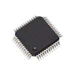
| 描述 | IC ADC 24BIT SRL 192KHZ 48-LQFP音频模/数转换器 IC 114dB 192kHz 8-Ch ADC w/TDM Interface |
| 产品分类 | |
| 品牌 | Cirrus Logic |
| 产品手册 | |
| 产品图片 |
|
| rohs | 符合RoHS无铅 / 符合限制有害物质指令(RoHS)规范要求 |
| 产品系列 | 音频 IC,音频模/数转换器 IC,Cirrus Logic CS5368-CQZ- |
| 数据手册 | |
| 产品型号 | CS5368-CQZ |
| 产品目录页面 | |
| 产品种类 | 音频模/数转换器 IC |
| 供应商器件封装 | 48-LQFP(7x7) |
| 信噪比 | 114 dB |
| 其它名称 | 598-1090 |
| 分辨率 | 24 bit |
| 分辨率(位) | 24 b |
| 功耗 | 680 mW |
| 包装 | 托盘 |
| 商标 | Cirrus Logic |
| 商标名 | CS5368 |
| 安装类型 | 表面贴装 |
| 安装风格 | SMD/SMT |
| 封装 | Tube |
| 封装/外壳 | 48-LQFP |
| 封装/箱体 | LQFP-48 |
| 工作温度 | -40°C ~ 85°C |
| 工作电源电压 | 5 V |
| 工厂包装数量 | 250 |
| 数据接口 | 串行 |
| 最大工作温度 | + 85 C |
| 最小工作温度 | - 40 C |
| 标准包装 | 250 |
| 电压-电源 | 3.3V,5V |
| 电压源 | 模拟和数字 |
| 电源电压-最大 | 5.25 V |
| 电源电压-最小 | 4.75 V |
| 类型 | ADC, 音频 |
| 系列 | CS5368 |
| 转换器数量 | 8 |
| 转换速率 | 192 kS/s |
| 配用 | /product-detail/zh/CDB5368/598-1157-ND/1245607 |
| 采样率(每秒) | 192k |


_renders/CS4265-CNZR.jpg)


- 商务部:美国ITC正式对集成电路等产品启动337调查
- 曝三星4nm工艺存在良率问题 高通将骁龙8 Gen1或转产台积电
- 太阳诱电将投资9.5亿元在常州建新厂生产MLCC 预计2023年完工
- 英特尔发布欧洲新工厂建设计划 深化IDM 2.0 战略
- 台积电先进制程称霸业界 有大客户加持明年业绩稳了
- 达到5530亿美元!SIA预计今年全球半导体销售额将创下新高
- 英特尔拟将自动驾驶子公司Mobileye上市 估值或超500亿美元
- 三星加码芯片和SET,合并消费电子和移动部门,撤换高东真等 CEO
- 三星电子宣布重大人事变动 还合并消费电子和移动部门
- 海关总署:前11个月进口集成电路产品价值2.52万亿元 增长14.8%


PDF Datasheet 数据手册内容提取
CS5368 114 dB, 192 kHz, 8-Channel A/D Converter Features Advanced Multi-bit Delta-Sigma Architecture Separate 1.8 V to 5 V Logic Supplies for Control and Serial Ports 24-Bit Conversion High-Pass Filter for DC Offset Calibration 114 dB Dynamic Range -105 dB THD+N Overflow Detection Supports Audio Sample Rates up to 216 kHz Footprint Compatible with the 4-Channel CS5364 and 6-Channel CS5366 Selectable Audio Interface Formats – Left-Justified, I²S, TDM Additional Control Port Features – 8-Channel TDM Interface Formats Supports I²C or SPI™ Control Interface per Low Latency Digital Filter specifications on page 17 and page 18 Less than 680 mW Power Consumption Individual Channel HPF Disable On-Chip Oscillator Driver Overflow Detection for Individual Channels Operation as System Clock Master or Slave Mute Control for Individual Channels Auto-Detect Speed in Slave Mode Independent Power-Down Control per Channel Differential Analog Architecture Pair VA VD VLC 5V 3.3 - 5V 1.8 - 5V Voltage Control Interface or Reference CoRnefiggiustreartsion I2oCr P, SinPsI Level anslat CDoenvticroel Tr Internal Oscillator A8n Dalioffge rIennptuiatsl Multi-bit Decimation High Pass APuSdCeiMori a Ool ru t Level anslator DAiugditiaol ADC Filter Filter TDM Tr VLS 1.8 - 5V Copyright Cirrus Logic, Inc. 2014 JUL '14 http://www.cirrus.com (All Rights Reserved) DS624F5
CS5368 Description The CS5368 is a complete 8-channel analog-to-digital converter for digital audio systems. It performs sampling, an- alog-to-digital conversion, and anti-alias filtering, generating 24-bit values for all 8-channel inputs in serial form at sample rates up to 216kHz per channel. The CS5368 uses a 5th-order, multi-bit delta sigma modulator followed by low latency digital filtering and decima- tion, which removes the need for an external anti-aliasing filter. The ADC uses a differential input architecture which provides excellent noise rejection. Dedicated level translators for the Serial Port and Control Port allow seamless interfacing between the CS5368 and other devices operating over a wide range of logic levels. In addition, an on-chip oscillator driver provides clocking flexibility and simplifies design. The CS5368 is the industry’s first audio A/D to support a high-speed TDM interface which provides a serial output of 8 channels of audio data with sample rates up to 216kHz within a single data stream. It further reduces layout complexity and relieves input/output constraints in digital signal processors. The CS5368 is available in a 48-pin LQFP package in both Commercial (-40°C to 85°C) and Automotive grades (-40°C to +105°C). The CDB5368 Customer Demonstration board is also available for device evaluation and implementation suggestions. Please see “Ordering Information” on page41 for complete ordering information. The CS5368 is ideal for high-end and pro-audio systems requiring unrivaled sound quality, transparent conversion, wide dynamic range and negligible distortion, such as A/V receivers, digital mixing consoles, multi-channel record- ers, outboard converters, digital effect processors, and automotive audio systems. 2 DS624F5
CS5368 TABLE OF CONTENTS 1. PIN DESCRIPTION .................................................................................................................................6 2. TYPICAL CONNECTION DIAGRAM ...................................................................................................9 3. CHARACTERISTICS AND SPECIFICATIONS ....................................................................................10 RECOMMENDED OPERATING CONDITIONS .................................................................................10 ABSOLUTE RATINGS .......................................................................................................................10 SYSTEM CLOCKING .........................................................................................................................10 DC POWER ........................................................................................................................................11 LOGIC LEVELS .................................................................................................................................11 PSRR, VQ AND FILT+ CHARACTERISTICS ....................................................................................11 ANALOG CHARACTERISTICS (COMMERCIAL) ..............................................................................12 ANALOG CHARACTERISTICS (AUTOMOTIVE) ...............................................................................13 DIGITAL FILTER CHARACTERISTICS .............................................................................................14 OVERFLOW TIMEOUT ......................................................................................................................14 SERIAL AUDIO INTERFACE - I²S/LJ TIMING ...................................................................................15 SERIAL AUDIO INTERFACE - TDM TIMING .....................................................................................16 SWITCHING SPECIFICATIONS - CONTROL PORT - I²C TIMING ...................................................17 SWITCHING SPECIFICATIONS - CONTROL PORT - SPI TIMING ..................................................18 4. APPLICATIONS ...................................................................................................................................19 4.1 Power .............................................................................................................................................19 4.2 Control Port Mode and Stand-Alone Operation ..............................................................................19 4.2.1 Stand-Alone Mode .................................................................................................................19 4.2.2 Control Port Mode .................................................................................................................19 4.3 Master Clock Source ......................................................................................................................20 4.3.1 On-Chip Crystal Oscillator Driver ..........................................................................................20 4.3.2 Externally Generated Master Clock .......................................................................................20 4.4 Master and Slave Operation ...........................................................................................................21 4.4.1 Synchronization of Multiple Devices ......................................................................................21 4.5 Serial Audio Interface (SAI) Format ................................................................................................22 4.5.1 I²S and LJ Format ..................................................................................................................22 4.5.2 TDM Format ..........................................................................................................................23 4.5.3 Configuring Serial Audio Interface Format ............................................................................23 4.6 Speed Modes .................................................................................................................................23 4.6.1 Sample Rate Ranges ............................................................................................................23 4.6.2 Using M1 and M0 to Set Sampling Parameters ....................................................................23 4.6.3 Master Mode Clock Dividers .................................................................................................24 4.6.4 Slave Mode Audio Clocking With Auto-Detect ......................................................................24 4.7 Master and Slave Clock Frequencies .............................................................................................25 4.8 Reset ..............................................................................................................................................27 4.8.1 Power-Down Mode ................................................................................................................27 4.9 Overflow Detection .........................................................................................................................27 4.9.1 Overflow in Stand-Alone Mode ..............................................................................................27 4.9.2 Overflow in Control Port Mode ..............................................................................................27 4.10 Analog Connections .....................................................................................................................28 4.11 Optimizing Performance in TDM Mode ........................................................................................29 4.12 DC Offset Control .........................................................................................................................29 4.13 Control Port Operation ..................................................................................................................30 4.13.1 SPI Mode .............................................................................................................................30 4.13.2 I²C Mode ..............................................................................................................................31 5. REGISTER MAP ...................................................................................................................................32 5.1 Register Quick Reference .............................................................................................................32 5.2 00h (REVI) Chip ID Code & Revision Register ...............................................................................32 DS624F5 3
CS5368 5.3 01h (GCTL) Global Mode Control Register ...................................................................................32 5.4 02h (OVFL) Overflow Status Register ...........................................................................................33 5.5 03h (OVFM) Overflow Mask Register ............................................................................................33 5.6 04h (HPF) High-Pass Filter Register .............................................................................................34 5.7 05h Reserved ................................................................................................................................34 5.8 06h (PDN) Power Down Register ..................................................................................................34 5.9 07h Reserved ................................................................................................................................34 5.10 08h (MUTE) Mute Control Register ..............................................................................................34 5.11 09h Reserved ..............................................................................................................................35 5.12 0Ah (SDEN) SDOUT Enable Control Register ............................................................................35 6. FILTER PLOTS .....................................................................................................................................36 7. PARAMETER DEFINITIONS ................................................................................................................39 8. PACKAGE DIMENSIONS ...................................................................................................................40 THERMAL CHARACTERISTICS .......................................................................................................40 9. ORDERING INFORMATION ................................................................................................................41 10. REVISION HISTORY .........................................................................................................................41 LIST OF FIGURES Figure 1. CS5368 Pinout .............................................................................................................................6 Figure 2. Typical Connection Diagram ........................................................................................................9 Figure 3. I²S/LJ Timing ..............................................................................................................................15 Figure 4. TDM Timing ...............................................................................................................................16 Figure 5. I²C Timing ..................................................................................................................................17 Figure 6. SPI Timing .................................................................................................................................18 Figure 7. Crystal Oscillator Topology ........................................................................................................20 Figure 8. Master/Slave Clock Flow ...........................................................................................................21 Figure 9. Master and Slave Clocking for a Multi-Channel Application ......................................................21 Figure 10. I²S Format ................................................................................................................................22 Figure 11. LJ Format .................................................................................................................................22 Figure 12. TDM Format .............................................................................................................................23 Figure 13. Master Mode Clock Dividers ....................................................................................................24 Figure 14. Slave Mode Auto-Detect Speed ...............................................................................................24 Figure 15. Recommended Analog Input Buffer .........................................................................................28 Figure 16. SPI Format ...............................................................................................................................30 Figure 17. I²C Write Format ......................................................................................................................31 Figure 18. I²C Read Format ......................................................................................................................31 Figure 19. SSM Passband ........................................................................................................................36 Figure 20. DSM Passband ........................................................................................................................36 Figure 21. QSM Passband ........................................................................................................................36 Figure 22. SSM Stopband .........................................................................................................................37 Figure 23. DSM Stopband .........................................................................................................................37 Figure 24. QSM Stopband ........................................................................................................................37 Figure 25. SSM -1 dB Cutoff .....................................................................................................................38 Figure 26. DSM -1 dB Cutoff ....................................................................................................................38 Figure 27. QSM -1 dB Cutoff .....................................................................................................................38 4 DS624F5
CS5368 LIST OF TABLES Table 1. Power Supply Pin Definitions ......................................................................................................19 Table 2. DIF1 and DIF0 Pin Settings ........................................................................................................23 Table 3. M1 and M0 Settings ....................................................................................................................23 Table 4. Frequencies for 48kHz Sample Rate using LJ/I²S .....................................................................25 Table 5. Frequencies for 96kHz Sample Rate using LJ/I²S .....................................................................25 Table 6. Frequencies for 192kHz Sample Rate using LJ/I²S ...................................................................25 Table 7. Frequencies for 48kHz Sample Rate using TDM .......................................................................25 Table 8. Frequencies for 48kHz Sample Rate using TDM .......................................................................25 Table 9. Frequencies for 96kHz Sample Rate using TDM .......................................................................26 Table 10. Frequencies for 96kHz Sample Rate using TDM .....................................................................26 Table 11. Frequencies for 192kHz Sample Rate using TDM ...................................................................26 Table 12. Frequencies for 192kHz Sample Rate using TDM ...................................................................26 DS624F5 5
CS5368 1. PIN DESCRIPTION T N U O K S DI L D C C C C C 0/ 1/ A/ L/ D D AIN1- AIN1+ AIN5- AIN5+ AIN6- AIN6+ MDIV RST M0/SD M1/SC DIF0/A DIF1/A 48 47 46 45 44 43 42 41 40 39 38 37 AIN2+ 1 36 OVFL AIN2- 2 35 VLC GND 3 34 CLKMODE VA 4 33 VD REF_GND 5 32 GND FILT+ 6 CS5368 31 SDOUT3/TDM VQ 7 30 SDOUT1/TDM GND 8 29 GND VA 9 28 VLS GND 10 27 SDOUT2 AIN4+ 11 26 SDOUT4 AIN4- 12 25 SCLK 13 14 15 16 17 18 19 20 21 22 23 24 AIN3+ AIN3- AIN7+ AIN7- AIN8+ AIN8- GND VX XTI XTO MCLK CK/FS R L Figure 1. CS5368 Pinout 6 DS624F5
CS5368 Pin Name Pin # Pin Description AIN2+, AIN2- 1,2 AIN4+, AIN4- 11,12 AIN3+, AIN3- 13,14 AIN7+, AIN7- 15,16 Differential Analog (Inputs) - Audio signals are presented differently to the delta sigma modula- AIN8+, AIN8- 17,18 tors via the AIN+/- pins. AIN6+, AIN6- 43,44 AIN5+, AIN5- 45,46 AIN1+, AIN1- 47,48 3,8 GND 10,19 Ground (Input) - Ground reference. Must be connected to analog ground. 29,32 VA 4,9 Analog Power (Input) - Positive power supply for the analog section Reference Ground (Input) - For the internal sampling circuits. Must be connected to analog REF_GND 5 ground. FILT+ 6 Positive Voltage Reference (Output) - Reference voltage for internal sampling circuits. VQ 7 Quiescent Voltage (Output) - Filter connection for the internal quiescent reference voltage. Crystal Oscillator Power (Input) - Also powers control logic to enable or disable oscillator cir- VX 20 cuits. XTI 21 Crystal Oscillator Connections (Input/Output) - I/O pins for an external crystal which may be XTO 22 used to generate MCLK. System Master Clock (Input/Output) - When a crystal is used, this pin acts as a buffered MCLK MCLK 23 Source (Output). When the oscillator function is not used, this pin acts as an input for the system master clock. In this case, the XTI and XTO pins must be tied low. Serial Audio Channel Clock (Input/Output) In I²S Mode, Serial Audio Channel Select. When low, the odd channels are selected. LRCK/FS 24 In LJ Mode, Serial Audio Channel Select. When high, the odd channels are selected. In TDM Mode, a frame sync signal. When high, it marks the beginning of a new frame of serial audio samples. In Slave Mode, this pin acts as an input pin. Main timing clock for the Serial Audio Interface (Input/Output) - During Master Mode, this pin SCLK 25 acts as an output, and during Slave Mode it acts as an input pin. SDOUT4 26 Serial Audio Data (Output) - Channels 7,8. SDOUT2 27 Serial Audio Data (Output) - Channels 3,4. VLS 28 Serial Audio Interface Power (Input) - Positive power for the serial audio interface. SDOUT1/TDM 30 Serial Audio Data (Output) - Channels 1,2. SDOUT3/TDM 31 Serial Audio Data (Output) - Channels 5,6. TDM is complementary TDM data. VD 33 Digital Power (Input) - Positive power supply for the digital section. VLC 35 Control Port Interface Power(Input) - Positive power for the control port interface. OVFL 36 Overflow (Output, open drain) - Detects an overflow condition on both left and right channels. RST 41 Reset (Input) - The device enters a low power mode when low. Stand-Alone Mode CLKMODE (Input) - Setting this pin HIGH places a divide-by-1.5 circuit in the MCLK path to the CLKMODE 34 core device circuitry. DIF1 37 DIF1, DIF0 (Input) - Inputs of the audio interface format. DIF0 38 M1 39 Mode Selection (Input) - Determines the operational mode of the device. M0 40 MCLK Divider (Input) - Setting this pin HIGH places a divide-by-2 circuit in the MCLK path to the MDIV 42 core device circuitry. DS624F5 7
CS5368 Control Port Mode CLKMODE (Input) - This pin is ignored in Control Port Mode and the same functionality is CLKMODE 34 obtained from the corresponding bit in the Global Control Register. Note: Should be connected to GND when using the part in Control Port Mode. I²C Format, AD1 (Input) - Forms the device address input AD[1]. AD1/CDIN 37 SPI Format, CDIN (Input) - Becomes the input data pin. I²C Format, AD0 (Input) - Forms the device address input AD[0]. AD0/CS 38 SPI Format, CS (Input) - Acts as the active low chip select input. I²C Format, SCL (Input) – Serial clock for the serial control port. An external pull-up resistor is SCL/CCLK 39 required for I²C control port operation. SPI Format, CCLK (Input) – Serial clock for the serial control port. I²C Format SDA (Input/Output) - Acts as an input/output data pin. An external pull-up resistor is SDA/CDOUT 40 required for I²C control port operation. SPI Format CDOUT (Output) - Acts as an output only data pin. MCLK Divider (Input) - This pin is ignored in Control Port Mode and the same functionality is MDIV 42 obtained from the corresponding bit in the Global Control Register. Note: Should be connected to GND when using the part in Control Port Mode. 8 DS624F5
CS5368 2. TYPICAL CONNECTION DIAGRAM Resistor may only be used if VD is derived from VA. If used, + +5V to 3.3V do not drive any other logic 1 F from VD. +5V + 1 F 0.0 1F 5.1 0.0 1F 4, 9 33 VA VD 6 FILT+ + 35 220F 0.1 F VLC +5V to 1.8V 5 REF_GND 0.01 F 7 VQ 1F+ 0.1 F MODE1/SCL/CCLK 39 8 GND MODE0/SDA/CDOUT 40 36 OVFL 37 Power Down DIF1/AD1/CDIN Channel 1 Analog 47 AIN 1+ DIF0/AD0/CS 38 and Mode Settings Input Buffer RST 41 48 AIN 1- MDIV 42 34 Channel 2 Analog 1 AIN 2+ CLKMODE Input Buffer 2 AIN 2- 13 Channel 3 Analog AIN 3+ CS5368 Input Buffer VLS 28 +5V to 1.8V 14 AIN 3- A/D CONVERTER 0.01 F Channel 4 Analog 11 AIN 4+ SDOUT1/ TDM 30 Input Buffer SDOUT2 27 12 AIN 4- SDOUT3/ TDM 31 APurodcioe Dssaotar 26 45 SDOUT4 Channel 5 Analog AIN 5+ Input Buffer LRCK/FS 24 46 AIN 5- SCLK 25 Timing Logic and Clock 43 MCLK 23 Channel 6 Analog AIN 6+ Input Buffer 44 AIN 6- 20 VX +5V 15 Channel 7 Analog AIN 7+ Input Buffer 21 XTI 16 AIN 7- 22 XTO 17 Channel 8 Analog AIN 8+ Input Buffer 18 AIN 8- GND 3, 8, 10, 19, 29, 32 Figure 2. Typical Connection Diagram For analog buffer configurations, refer to Cirrus Application Note AN241. Also, a low-cost single-ended-to-differen- tial solution is provided on the Customer Evaluation Board. DS624F5 9
CS5368 3. CHARACTERISTICS AND SPECIFICATIONS RECOMMENDED OPERATING CONDITIONS GND = 0V, all voltages with respect to 0V. Parameter Symbol Min Typ Max Unit DC Power Supplies: Positive Analog VA 4.75 5.0 Positive Crystal VX 4.75 5.0 Positive Digital VD 3.14 3.3 5.25 V Positive Serial Logic VLS 1.711 3.3 Positive Control Logic VLC 1.71 3.3 Ambient Operating Temperature (-CQZ) T -40 - 85 AC °C (-DQZ) T -40 - 105 AA 1. TDM Quad-Speed Mode specified to operate correctly at VLS 3.14V. ABSOLUTE RATINGS Operation beyond these limits may result in permanent damage to the device. Normal operation is not guaranteed at these extremes. Transient currents up to ±100 mA on the analog input pins will not cause SCR latch-up. Parameter Symbol Min Typ Max Units DC Power Supplies: Positive Analog VA Positive Crystal VX Positive Digital VD -0.3 - +6.0 V Positive Serial Logic VLS Positive Control Logic VLC Input Current I -10 10 mA in Analog Input Voltage V VA+0.3 IN -0.3 V Digital Input Voltage V - VL+0.3 IND Ambient Operating Temperature (Power Applied) T -50 +125 A C Storage Temperature T -65 +150 stg SYSTEM CLOCKING Parameter Symbol Min Typ Max Unit Input Master Clock Frequency MCLK 0.512 55.05 MHz Input Master Clock Duty Cycle t 40 60 % clkhl 10 DS624F5
CS5368 DC POWER MCLK = 12.288MHz; Master Mode; GND = 0V. Parameter Symbol Min Typ Max Unit Power Supply Current VA = 5V I 100 112 A (Normal Operation) VX = 5V I 4 8 X VD = 5V I 70 88 D - mA VD = 3.3V I 42 50 D VLS, VLC = 5V I 12 15 L VLS, VLC = 3.3V I 5 8 L Power Supply Current VA = VX = 5V I 50 A - - A (Power-Down) (Note 1) VLS, VLC, VD = 5V I 500 D+L Power Consumption Normal Operation All Supplies = 5V 930 1115 - - mW VA = VX = 5V, VD = VLS = VLC = 3.3V 675 792 (Power-Down) (Note 1) 2.75 - 1. Power-Down is defined as RST = LOW with all clocks and data lines held static at a valid logic level. LOGIC LEVELS Parameter Symbol Min Typ Max Units High-Level Input Voltage %VLS/VLC V 70 - - % IH Low-Level Input Voltage %VLS/VLC V - - 30 % IL High-Level Output Voltage at 100 A load %VLS/VLC V 85 - - % OH Low-Level Output Voltage at -100 A load %VLS/VLC V - - 15 % OL SDA Low-Level Output Voltage at -2 mA load %VLC V - - TBD % OL OVFL Current Sink -4 mA Input Leakage Current logic pins only I -10 - 10 A in PSRR, VQ AND FILT+ CHARACTERISTICS MCLK = 12.288MHz; Master Mode. Valid with the recommended capacitor values on FILT+ and VQ as shown in the “Typical Connection Diagram”. Parameter Symbol Min Typ Max Unit Power Supply Rejection Ratio at (1 kHz) PSRR - 65 - dB V Nominal Voltage VA/2 V Q Output Impedance - 25 - k Maximum allowable DC current source/sink 10 A Filt+ Nominal Voltage VA V Output Impedance - 4.4 - k Maximum allowable DC current source/sink 10 A DS624F5 11
CS5368 ANALOG CHARACTERISTICS (COMMERCIAL) Test Conditions (unless otherwise specified). VA = 5 V, VD = VLS = VLC 3.3 V, and T = 25° C. Full-scale input A sine wave. Measurement Bandwidth is 10Hz to 20kHz. Parameter Symbol Min Typ Max Unit Single-Speed Mode Fs = 48kHz Dynamic Range A-weighted 108 114 - dB unweighted 105 111 - Total Harmonic Distortion + Noise -1dB -105 -99 referred to typical full scale -20dB THD+N - -91 - dB -60dB -51 -45 Double-Speed Mode Fs = 96kHz Dynamic Range A-weighted 108 114 unweighted 105 111 - dB 40kHz bandwidth unweighted - 108 Total Harmonic Distortion + Noise -1dB -105 -99 referred to typical full scale -20dB -91 - THD+N - dB -60dB -51 -45 40kHz bandwidth -1dB -102 - Quad-Speed Mode Fs = 192kHz Dynamic Range A-weighted 108 114 unweighted 105 111 - dB 40kHz bandwidth unweighted - 108 Total Harmonic Distortion + Noise -1dB -105 -99 referred to typical full scale -20dB -91 - THD+N - dB -60dB -51 -45 40kHz bandwidth -1dB -102 - Dynamic Performance for All Modes Interchannel Isolation - 110 - dB DC Accuracy Interchannel Gain Mismatch - 0.1 - dB Gain Error -5 - 5 % Gain Drift - 100 - ppm/°C Offset Error HPF enabled 0 - - LSB HPF disabled - - 100 Analog Input Characteristics Full-scale Differential Input Voltage 1.07*VA 1.13*VA 1.19*VA Vpp Input Impedance (Differential) - 250 - k Common Mode Rejection Ratio CMRR - 82 - dB 12 DS624F5
CS5368 ANALOG CHARACTERISTICS (AUTOMOTIVE) Test Conditions (unless otherwise specified). VA = 5.25 to 4.75 V, VD = 5.25 to 3.14V, VLS = VLC = 5.25 to 1.71V and T =-40° to +85°C. Full-scale input sine wave. Measurement Bandwidth is 10Hz to 20kHz. A Parameter Symbol Min Typ Max Unit Single-Speed Mode Fs = 48kHz Dynamic Range A-weighted 106 114 - dB unweighted 103 111 Total Harmonic Distortion + Noise -1dB -105 -97 referred to typical full scale -20dB THD+N - -91 - dB -60dB -51 -45 Double-Speed Mode Fs = 96kHz Dynamic Range A-weighted 106 114 unweighted 103 111 - dB 40kHz bandwidth unweighted - 108 Total Harmonic Distortion + Noise -1dB -105 -97 referred to typical full scale -20dB -91 - THD+N - dB -60dB -51 -45 40kHz bandwidth -1dB -102 - Quad-Speed Mode Fs = 192kHz Dynamic Range A-weighted 106 114 unweighted 103 111 - dB 40kHz bandwidth unweighted - 108 Total Harmonic Distortion + Noise -1dB -105 -97 referred to typical full scale -20dB -91 - THD+N - dB -60dB -51 -45 40kHz bandwidth -1dB -102 - Dynamic Performance for All Modes Interchannel Isolation - 110 - dB DC Accuracy Interchannel Gain Mismatch - 0.1 - dB Gain Error -7 - 7 % Gain Drift - 100 - ppm/°C Offset Error HPF enabled 0 - - LSB HPF disabled - - 100 Analog Input Characteristics Full-scale Input Voltage 1.02*VA 1.13*VA 1.24*VA Vpp Input Impedance (Differential) 250 - k Common Mode Rejection Ratio CMRR - 82 - dB DS624F5 13
CS5368 DIGITAL FILTER CHARACTERISTICS Parameter Symbol Min Typ Max Unit Single-Speed Mode (2kHz to 54kHz sample rates) Passband (Note 1) (-0.1dB) 0 0.47 Fs Passband Ripple -0.035 0.035 dB - Stopband (Note 1) 0.58 Fs Stopband Attenuation -95 - dB Total Group Delay (Fs = Output Sample Rate) t - 12/Fs s gd Double-Speed Mode (54kHz to 108kHz sample rates) Passband (Note 1) (-0.1dB) 0 0.45 Fs Passband Ripple -0.035 0.035 dB - Stopband (Note 1) 0.68 Fs Stopband Attenuation -92 - dB Total Group Delay (Fs = Output Sample Rate) t - 9/Fs s gd Quad-Speed Mode (108kHz to 216kHz sample rates) Passband (Note 1) (-0.1dB) 0 0.24 Fs Passband Ripple -0.035 0.035 dB - Stopband (Note 1) 0.78 Fs Stopband Attenuation -92 - dB Total Group Delay (Fs = Output Sample Rate) t - 5/Fs s gd High-Pass Filter Characteristics Frequency Response (Note 2) -3.0dB 1 - - Hz -0.13dB 20 Phase Deviation (Note 2) @ 20Hz 10 - Deg Passband Ripple - - 0 dB Filter Settling Time 105/Fs - s Notes: 1. The filter frequency response scales precisely with Fs. 2. Response shown is for Fs equal to 48 kHz. Filter characteristics scale with Fs. OVERFLOW TIMEOUT Logic "0" = GND = 0V; Logic "1" = VLS; C = 30pF, timing threshold is 50% of VLS. L Parameter Symbol Min Typ Max Unit OVFL time-out on overrange condition (217-1)/Fs Fs = 44.1kHz - 2972 - ms Fs = 192kHz 683 14 DS624F5
CS5368 SERIAL AUDIO INTERFACE - I²S/LJ TIMING The serial audio port is a three-pin interface consisting of SCLK, LRCK and SDOUT. Logic "0" = GND = 0V; Logic "1" = VLS; C = 20pF, timing threshold is 50% of VLS. L Parameter Symbol Min Typ Max Unit Sample Rates Single-Speed Mode 2 54 Double-Speed Mode - 54 - 108 kHz Quad-Speed Mode 108 216 Master Mode SCLK Frequency - 64*Fs - 64*Fs Hz SCLK Period 1/(64*216kHz) t 72.3 - - ns PERIOD SCLK Duty Cycle (Note 1) (CLKMODE = 0)(Note 2) tHIGH 40 50 60 % t 28 33 38 % (CLKMODE = 1)(Note 2) HIGH LRCK setup before SCLK rising t 20 SETUP1 - - ns LRCK hold after SCLK rising t 20 HOLD1 SDOUT setup before SCLK rising t 10 SETUP2 SDOUT hold after SCLK rising (VLS = 1.8 V) t 20 HOLD2 - - ns after SCLK rising (VLS = 3.3 V) t 10 HOLD2 after SCLK rising (VLS = 5 V) t 5 HOLD2 Slave Mode SCLK Frequency (Note 3) - - 64*Fs - Hz SCLK Period 1/(64*216kHz) tPERIOD 72.3 - - ns SCLK Duty Cycle tHIGH 28 - 65 % LRCK setup before SCLK rising t 20 SETUP1 - - ns LRCK hold after SCLK rising t 20 HOLD1 SDOUT setup before SCLK rising (VLS = 1.8 V) t 4 SETUP2 before SCLK rising (VLS = 3.3 V) t 10 SETUP2 before SCLK rising (VLS = 5 V) t 10 SETUP2 - - ns SDOUT hold after SCLK rising (VLS = 1.8 V) t 20 HOLD2 after SCLK rising (VLS = 3.3 V) t 10 HOLD2 after SCLK rising (VLS = 5 V) t 5 HOLD2 Notes: 1. Duty cycle of generated SCLK depends on duty cycle of received MCLK as specified under “System Clocking” on page10. 2. CLKMODE functionality described in Section 4.6.3 "Master Mode Clock Dividers" on page 24. 3. In Slave Mode, the SCLK/LRCK ratio can be set according to preference. However, chip performance is guaranteed only when using the ratios in Section 4.7 Master and Slave Clock Frequencies on page 25. t t PERIOD HIGH SCLK t t HOLD1 SETUP1 LRCK channel channel t t SETUP2 HOLD2 SDOUT data data Figure 3. I²S/LJ Timing DS624F5 15
CS5368 SERIAL AUDIO INTERFACE - TDM TIMING The serial audio port is a three-pin interface consisting of SCLK, LRCK and SDOUT. Logic "0" = GND = 0V; Logic "1" = VLS; C = 20pF, timing threshold is 50% of VLS. L Parameter Symbol Min Typ Max Unit Sample Rates Single-Speed Mode - 2 - 54 kHz Double-Speed Mode - 54 - 108 kHz Quad-Speed Mode1 - 108 - 216 kHz Master Mode SCLK Frequency 256*Fs - 256*Fs Hz SCLK Period 1/(256*216kHz) t 18 - - ns PERIOD SCLK Duty Cycle (Note 2) (CLKMODE = 0)(Note 3) t 40 50 60 % HIGH1 (CLKMODE = 1)(Note 3) t 28 33 38 % HIGH1 FS setup before SCLK rising (Single-Speed Mode) t 20 - - ns SETUP1 FS setup before SCLK rising (Double-Speed Mode) t 18 - - ns SETUP1 FS setup before SCLK rising (Quad-Speed Mode) t 5 - - ns SETUP1 FS width in SCLK cycles t 128 - 128 - HIGH2 SDOUT setup before SCLK rising t 5 - - ns SETUP2 SDOUT hold after SCLK rising t 5 - - ns HOLD2 Slave Mode SCLK Frequency (Note 4) - 256*Fs - Hz SCLK Period 1/(256*216kHz) t 18 - - ns PERIOD SCLK Duty Cycle t 28 - 65 % HIGH1 FS setup before SCLK rising (Single-Speed Mode) t 20 - - ns SETUP1 FS setup before SCLK rising (Double-Speed Mode) t 20 - - ns SETUP1 FS setup before SCLK rising (Quad-Speed Mode) t 10 - - ns SETUP1 FS width in SCLK cycles t 1 - 244 - HIGH2 SDOUT setup before SCLK rising t 5 - - ns SETUP2 SDOUT hold after SCLK rising t 5 - - ns HOLD2 Notes: 1. TDM Quad-Speed Mode only specified to operate correctly at VLS 3.14V. 2. Duty cycle of generated SCLK depends on duty cycle of received MCLK as specified under “System Clocking” on page10. 3. CLKMODE functionality described in Section 4.6.3 "Master Mode Clock Dividers" on page 24. 4. In Slave Mode, the SCLK/LRCK ratio can be set according to preference; chip performance is guaran- teed only when using the ratios in Section 4.7 Master and Slave Clock Frequencies on page 25. t t PERIOD HIGH1 SCLK t HIGH2 t SETUP1 FS new frame t t SETUP2 HOLD2 SDOUT data data data Figure 4. TDM Timing 16 DS624F5
CS5368 SWITCHING SPECIFICATIONS - CONTROL PORT - I²C TIMING Inputs: Logic 0=DGND, Logic 1=VLC, SDA C =30pF L Parameter Symbol Min Max Unit SCL Clock Frequency f - 100 kHz scl RST Rising Edge to Start t 600 ns irs Bus Free Time Between Transmissions t 4.7 µs buf Start Condition Hold Time (prior to first clock pulse) t 4.0 hdst Clock Low time t 4.7 low - Clock High Time thigh 4.0 µs Setup Time for Repeated Start Condition t 4.7 sust SDA Hold Time from SCL Falling (Note 1) thdd 0 SDA Setup time to SCL Rising (Note 2) t 600 ns sud Rise Time of SCL and SDA t - 1 µs rc Fall Time SCL and SDA t - 300 ns fc Setup Time for Stop Condition t 4.7 - µs susp Acknowledge Delay from SCL Falling t 300 1000 ns ack Notes: 1. Data must be held for sufficient time to bridge the transition time, t , of SCL. fc RST t irs Repeated Stop Start Start Stop trd tfd SDA tbuf thdst t high thdst tfc tsusp SCL tlow t hdd tsud tack tsust trc Figure 5. I²C Timing 2. The operational timing specification deviates from the I2C-Bus Specification and User Manual of 250ns. DS624F5 17
CS5368 SWITCHING SPECIFICATIONS - CONTROL PORT - SPI TIMING Inputs: Logic 0=DGND, Logic 1=VLC, CDOUT C =30pF L Parameter Symbol Min Max Units CCLK Clock Frequency f 0 6.0 MHz sck RST Rising Edge to CS Falling t 20 srs ns CS Falling to CCLK Edge t 20 css CS High Time Between Transmissions t 1.0 s csh CCLK Low Time t 66 - scl CCLK High Time t 66 sch CDIN to CCLK Rising Setup Time t 40 dsu CCLK Rising to DATA Hold Time (Note 1) t 15 dh CCLK Falling to CDOUT Stable t 50 ns pd Rise Time of CDOUT t r1 25 Fall Time of CDOUT t - f1 Rise Time of CCLK and CDIN (Note 2) t r2 100 Fall Time of CCLK and CDIN (Note 2) t f2 Notes: 1. Data must be held for sufficient time to bridge the transition time of CCLK. 2. For f <1MHz sck RST t srs CS t csh t t t css sch scl t r2 CCLK t f2 t t dsu dh CDIN t pd CDOUT Figure 6. SPI Timing 18 DS624F5
CS5368 4. APPLICATIONS 4.1 Power CS5368 features five independent power pins that power various functional blocks within the device and allow for convenient interfacing to other devices. Table1 shows what portion of the device is powered from each supply pin. Please refer to “Recommended Operating Conditions” on page10 for the valid range of each power supply pin. The power supplied to each power pin can be independent of the power supplied to any other pin. Power Supply Pin Pin Name Pin Number Functional Block VA 4, 9 Analog Core VX 20 Crystal Oscillator VD 33 Digital Core VLS 28 Serial Audio Interface VLC 35 Control Logic Table 1. Power Supply Pin Definitions To meet full performance specifications, the CS5368 requires normal low-noise board layout. The “Typical Connection Diagram” on page9 shows the recommended power arrangements, with the VA pins connected to a clean supply. VD, which powers the digital filter, may be run from the system logic supply, or it may be powered from the analog supply via a single-pole decoupling filter. Decoupling capacitors should be placed as near to the ADC as possible, with the lower value high-frequen- cy capacitors placed nearest to the device leads. Clocks should be kept away from the FILT+ and VQ pins in order to avoid unwanted coupling of these signals into the device. The FILT+ and VQ decoupling capac- itors must be positioned to minimize the electrical path to ground. The CDB5368 evaluation board demonstrates optimum layout for the device. 4.2 Control Port Mode and Stand-Alone Operation 4.2.1 Stand-Alone Mode In Stand-Alone Mode, the CS5368 is programmed exclusively with multi-use configuration pins. This mode provides a set of commonly used features, which comprise a subset of the complete set of device features offered in Control Port Mode. To use the CS5368 in Stand-Alone Mode, the configuration pins must be held in a stable state, at valid logic levels, and RST must be asserted until the power supplies and clocks are stable and valid. More informa- tion on the reset function is available in Section 4.5 on page 22. 4.2.2 Control Port Mode In Control Port Mode, all features of the CS5368 are available. Four multi-use configuration pins become software pins that support the I²C or SPI bus protocol. To initiate Control Port Mode, a controller that sup- ports I²C or SPI must be used to enable the internal register functionality. This is done by setting the CP- EN bit (Bit 7 of the Global Control Port Register). Once CP-EN is set, all of the device configuration pins are ignored, and the internal register settings determine the operating modes of the part. Figure 4.13 on page 30 provides detailed information about the I²C and SPI bus protocols. DS624F5 19
CS5368 4.3 Master Clock Source The CS5368 requires a Master Clock that can come from one of two sources: an on-chip crystal oscillator driver or an externally generated clock. 4.3.1 On-Chip Crystal Oscillator Driver When using the on-board crystal oscillator driver, the XTI pin (pin 21) is the input for the Master Clock (MC- LK) to the device. The XTO pin (pin 22) must not be used to drive anything other than the oscillator tank circuitry. When using the on-board crystal driver, the topology shown in Figure7 must be used. The crystal oscillator manufacturer supplies recommended capacitor values. A buffered copy of the XTI input is avail- able as an output on the MCLK pin (pin 23), which is level-controlled by VLS and may be used to synchro- nize other parts to the device. 21 XTI 22 XTO Figure 7. Crystal Oscillator Topology 4.3.2 Externally Generated Master Clock If an external clock is used, the XTI and XTO pins must be grounded, and the MCLK pin becomes an input for the system master clock. The incoming MCLK should be at the logic level set by the user on the VLS supply pin. 20 DS624F5
CS5368 4.4 Master and Slave Operation CS5368 operation depends on two clocks that are synchronously derived from MCLK: SCLK and LRCK/FS. See Section 4.5 on page 22 for a detailed description of SCLK and LRCK/FS. The CS5368 can operate as either clock master or clock slave with respect to SCLK and LRCK/FS. In Mas- ter Mode, the CS5368 derives SCLK and LRCK/FS synchronously from MCLK and outputs the derived clocks on the SCLK pin (pin 25) and the LRCK/FS pin (pin 24), respectively. In Slave Mode, the SCLK and LRCK/FS are inputs, and the input signals must be synchronously derived from MCLK by a separate device such as another CS5368 or a microcontroller. Figure8 illustrates the clock flow of SCLK and LRCK/FS in both Master and Slave Modes. The Master/Slave operation is controlled through the settings of M1 and M0 pins in Stand-Alone Mode or by the M[1] and M[0] bits in the Global Mode Control Register in Control Port Mode. See Section 4.6 on page 23 for more information regarding the configuration of M1 and M0 pins or M[1] and M[0] bits. SCLK SCLK ADC as ADC as clock Controller clock Controller master LRCK/FS slave LRCK/FS Figure 8. Master/Slave Clock Flow 4.4.1 Synchronization of Multiple Devices To ensure synchronous sampling in applications where multiple ADCs are used, the MCLK and LRCK must be the same for all CS5368 devices in the system. If only one master clock source is needed, one solution is to place one CS5368 in Master Mode, and slave all of the other devices to the one master, as illustrated in Figure9. If multiple master clock sources are needed, one solution is to supply all clocks from the same external source and time the CS5368 reset de-assertion with the falling edge of MCLK. This will ensure that all converters begin sampling on the same clock edge. SCLK & LRCK/FS Master Slave1 ADC ADC Slave2 ADC Slave3 ADC Figure 9. Master and Slave Clocking for a Multi-Channel Application DS624F5 21
CS5368 4.5 Serial Audio Interface (SAI) Format The SAI port consists of two timing pins (SCLK, LRCK/FS) and four audio data output pins (SDOUT1/TDM, SDOUT2, SDOUT3/TDM and SDOUT4). The CS5368 output is serial data in I²S, Left-Justified (LJ), or Time Division Multiplexed (TDM) digital audio interface formats. These formats are available to the user in both Stand-Alone Mode and Control Port Mode. 4.5.1 I²S and LJ Format The I²S and LJ formats are both two-channel protocols. During one LRCK period, two channels of data are transmitted, odd channels first, then even. The MSB is always clocked out first. In Slave Mode, the number of SCLK cycles per channel is fixed as described under “Serial Audio Interface - I²S/LJ Timing” on page15. In Slave Mode, if more than 32 SCLK cycles per channel are received from a master controller, the CS5368 will fill the longer frame with trailing zeros. If fewer than 24 SCLK cycles per channel are received from a master, the CS5368 will truncate the serial data output to the number of SCLK cycles received. For a complete overview of serial audio interface formats, please refer to Cirrus Logic Ap- plication Note AN282. receiver latches data on rising edges of SCLK SCLK LRCK Odd Channels 1,3, ... Even Channels 2,4, ... SDOUT MSB ... LSB MSB ... LSB MSB Figure 10. I²S Format receiver latches data on rising edges of SCLK SCLK LRCK Odd Channels 1,3, ... Even Channels 2,4, ... SDOUT MSB ... LSB MSB ... LSB MSB Figure 11. LJ Format 22 DS624F5
CS5368 4.5.2 TDM Format In TDM Mode, all eight channels of audio data are serially clocked out during a single Frame Sync (FS) cycle, as shown in Figure12. The rising edge of FS signifies the start of a new TDM frame cycle. Each channel slot occupies 32 SCLK cycles, with the data left justified and with MSB first. TDM output data should be latched on the rising edge of SCLK within time specified under ”Serial Audio Interface - TDM Tim- ing” section on page16. The TDM data output port resides on the SDOUT1 pin. The TDM output pin is complimentary TDM data. All SDOUT pins will remain active during TDM Mode. Refer to Section 4.11 “Op- timizing Performance in TDM Mode” on page29 for critical system design information. FS SCLK TDM OUT LSB MSB LSB MSB LSB MSB LSB MSB LSB MSB LSB MSB LSB MSB LSB MSB LSB MSB Channel 1 Channel 2 Channel 3 Channel 4 Channel 5 Channel 6 Channel 7 Channel 8 32 clks 32 clks 32 clks 32 clks 32 clks 32 clks 32 clks 32 clks Data MSB LSB Zeroes Figure 12. TDM Format 4.5.3 Configuring Serial Audio Interface Format The serial audio interface format of the data is controlled by the configuration of the DIF1 and DIF0 pins in Stand-Alone Mode or by the DIF[1] and DIF[0] bits in the Global Mode Control Register in Control Port Mode, as shown in Table2. DIF1 DIF0 Mode 0 0 Left-Justified 0 1 I²S 1 0 TDM 1 1 Reserved Table 2. DIF1 and DIF0 Pin Settings 4.6 Speed Modes 4.6.1 Sample Rate Ranges CS5368 supports sampling rates from 2kHz to 21 kHz, divided into three ranges: 2kHz-54kHz, 54kHz- 108kHz, and 108kHz-216 kHz. These sampling speed modes are called Single-Speed Mode (SSM), Double-Speed Mode (DSM), and Quad-Speed Mode (QSM), respectively. 4.6.2 Using M1 and M0 to Set Sampling Parameters The Master/Slave operation and the sample rate range are controlled through the settings of the M1 and M0 pins in Stand-Alone Mode, or by the M[1] and M[0] bits in the Global Mode Control Register in Control Port Mode, as shown in Table3. M1 M0 Mode Frequency Range 0 0 Single-Speed Master Mode (SSM) 2kHz - 54kHz 0 1 Double-Speed Master Mode (DSM) 54kHz - 108kHz 1 0 Quadruple-Speed Master Mode (QSM) 108kHz - 216kHz 1 1 Auto-Detected Speed Slave Mode 2kHz - 216kHz Table 3. M1 and M0 Settings DS624F5 23
CS5368 4.6.3 Master Mode Clock Dividers Figure13 shows the configuration of the MCLK dividers and the sample rate dividers for Master Mode, in- cluding the significance of each MCLK divider pin (in Stand-Alone Mode) or bit (in Control Port Mode). SAMPLE RATE DIVIDERS Single ÷ 256 00 Speed Double MCLK DIVIDERS ÷ 128 01 LRCK/ FS Speed ÷ 64 Quad 10 Speed 0/1 0/1 0/1 ÷ 1 ÷ 1 ÷ 1 MCLK M1 M0 ÷ 1.5 ÷ 2 ÷ 2 Single ÷ 4 00 Speed pin CLKMODE MDIV n/a ÷ 2 Double 01 SCLK bit CLKMODE MDIV1 MDIV0 Speed Quad ÷ 1 10 Speed Figure 13. Master Mode Clock Dividers 4.6.4 Slave Mode Audio Clocking With Auto-Detect In Slave Mode, CS5368 auto-detects speed mode, which eliminates the need to configure M1 and M0 when changing among speed modes. The external MCLK is subject to clock dividers as set by the clock divider pins in Stand-Alone Mode or the clock divider bits in Control Port Mode. The CS5368 compares the divided- down, internal MCLK to the incoming LRCK/FS and sets the speed mode based on the MCLK/LRCK ratio as shown in Figure14. MCLK DIVIDERS SPEED MODE 0/1 0/1 0/1 256 Single-Speed Internal ÷ 1 ÷ 1 ÷ 1 External MCLK ÷LRCK 128 Double-Speed MCLK ÷ 1.5 ÷ 2 ÷ 2 64 Quad-Speed pin CLKMODE MDIV n/a LRCK bit CLKMODE MDIV1 MDIV0 Figure 14. Slave Mode Auto-Detect Speed 24 DS624F5
CS5368 4.7 Master and Slave Clock Frequencies Tables 4 through 12 show the clock speeds for sample rates of 48kHz, 96kHz and 192kHz. The MC- LK/LRCK ratio should be kept at a constant value during each mode. In Master Mode, the device outputs the frequencies shown. In Slave Mode, the SCLK/LRCK ratio can be set according to design preference. However, device performance is guaranteed only when using the ratios shown in the tables. Control Port Mode only LJ/I²S MASTER OR SLAVE SSM Fs = 48 kHz MCLK Divider 4 3 2 1.5 1 MCLK (MHz) 49.152 36.864 24.576 18.384 12.288 SCLK (MHz) 3.072 3.072 3.072 3.072 3.072 MCLK/LRCK Ratio 1024 768 512 384 256 SCLK/LRCK Ratio 64 64 64 64 64 Table 4. Frequencies for 48kHz Sample Rate using LJ/I²S LJ/I²S MASTER OR SLAVE DSM Fs = 96 kHz MCLK Divider 4 3 2 1.5 1 MCLK (MHz) 49.152 36.864 24.567 18.384 12.288 SCLK (MHz) 6.144 6.144 6.144 6.144 6.144 MCLK/LRCK Ratio 512 384 256 192 128 SCLK/LRCK Ratio 64 64 64 64 64 Table 5. Frequencies for 96kHz Sample Rate using LJ/I²S LJ/I²S MASTER OR SLAVE QSM Fs = 192 kHz MCLK Divider 4 3 2 1.5 1 MCLK (MHz) 49.152 36.864 24 18.384 12.288 SCLK (MHz) 12.288 12.288 12.288 12.288 12.288 MCLK/LRCK Ratio 256 192 128 96 64 SCLK/LRCK Ratio 64 64 64 64 64 Table 6. Frequencies for 192kHz Sample Rate using LJ/I²S TDM MASTER SSM Fs = 48 kHz MCLK Divider 4 3 2 1.5 1 MCLK (MHz) 49.152 36.864 24.567 18.384 12.288 SCLK (MHz) 12.288 12.288 12.288 12.288 12.288 MCLK/FS Ratio 1024 768 512 384 256 SCLK/FS Ratio 256 256 256 256 256 Table 7. Frequencies for 48kHz Sample Rate using TDM TDM SLAVE SSM Fs = 48 kHz MCLK Divider 4 3 2 1.5 1 MCLK (MHz) 49.152 36.864 24.567 18.384 12.288 SCLK (MHz) 12.288 12.288 12.288 12.288 12.288 MCLK/FS Ratio 1024 768 512 384 256 SCLK/FS Ratio 256 256 256 256 256 Table 8. Frequencies for 48kHz Sample Rate using TDM DS624F5 25
CS5368 TDM MASTER DSM Fs = 96 kHz MCLK Divider 4 3 2 - - MCLK (MHz) 49.152 36.864 24.567 - - SCLK (MHz) 24.576 24.576 24.576 - - MCLK/FS Ratio 512 384 256 - - SCLK/FS Ratio 256 256 256 - - Table 9. Frequencies for 96kHz Sample Rate using TDM TDM SLAVE DSM Fs = 96 kHz MCLK Divider 4 3 2 1.5 1 MCLK (MHz) 49.152 36.864 24.567 18.384 12.288 SCLK (MHz) 24.576 24.576 24.576 24.576 24.576 MCLK/FS Ratio 512 384 256 192 128 SCLK/FS Ratio 256 256 256 256 256 Table 10. Frequencies for 96kHz Sample Rate using TDM TDM MASTER QSM Fs = 192 kHz MCLK Divider 4 - - - - MCLK (MHz) 49.152 - - - - SCLK (MHz) 49.152 - - - - MCLK/FS Ratio 256 - - - - SCLK/FS Ratio 256 - - - - Table 11. Frequencies for 192kHz Sample Rate using TDM TDM SLAVE QSM Fs = 192 kHz MCLK Divider 4 3 2 1.5 1 MCLK (MHz) 49.152 36.864 24.567 18.384 12.288 SCLK (MHz) 49.152 49.152 49.152 49.152 49.152 MCLK/FS Ratio 256 192 128 96 64 SCLK/FS Ratio 256 256 256 256 256 Table 12. Frequencies for 192kHz Sample Rate using TDM 26 DS624F5
CS5368 4.8 Reset The device should be held in reset until power is applied and all incoming clocks are stable and valid. Upon de-assertion of RST, the state of the configuration pins is latched, the state machine begins, and the device starts sending audio output data a maximum of 524288 MCLK cycles after the release of RST. When chang- ing between mode configurations in Stand-Alone Mode, including clock dividers, serial audio interface for- mat, master/slave, or speed modes, it is recommended to reset the device following the change by holding the RST pin low for a minimum of one MCLK cycle and then restoring the pin to a logic-high condition. 4.8.1 Power-Down Mode The CS5368 features a Power-Down Mode in which power is temporarily withheld from the modulators, the crystal oscillator driver, the digital core, and the serial port. The user can access Power-Down Mode by holding the device in reset and holding all clock lines at a static, valid logic level (either logic-high or logic- low). “DC Power” on page11 shows the power-saving associated with Power-Down Mode. 4.9 Overflow Detection 4.9.1 Overflow in Stand-Alone Mode The CS5368 includes overflow detection on all input channels. In Stand-Alone Mode, this information is presented as open drain, active low on the OVFL pin. The pin will go to a logical low as soon as an over- range condition in any channel is detected. The data will remain low, then time-out as specified in Section "Overflow Timeout" on page 14. After the time-out, the OVFL pin will return to a logical high if there has not been any other over-range condition detected. Note that an over-range condition on any channel will restart the time-out period. 4.9.2 Overflow in Control Port Mode In Control Port Mode, the Overflow Status Register interacts with the Overflow Mask Register to provide interrupt capability for each individual channel. See Section 5.4 "02h (OVFL) Overflow Status Register" on page 33 for details on these two registers. DS624F5 27
CS5368 4.10 Analog Connections The analog modulator samples the input at half of the internal Master Clock frequency, or 6.144 MHz nom- inally. The digital filter will reject signals within the stopband of the filter. However, there is no rejection of input signals that are at (N X 6.144 MHz) the digital passband frequency, where n=0,1,2.... Refer to Figure15, which shows the suggested filter that will attenuate any noise energy at 6.144 MHz in addition to providing the optimum source impedance for the modulators. The use of capacitors that have a large volt- age coefficient (such as general-purpose ceramics) must be avoided since these can degrade signal linear- ity. COG capacitors are recommended for this application. For additional configurations, refer to Cirrus Application Note AN241. 634 470 pF COG - 91 10 uF ADC AIN+ AIN+ + 100k 10k COG VQ 2700 pF 10k 10 uF AIN- + 91 ADC AIN- 100k - 470 pF COG 634 Figure 15. Recommended Analog Input Buffer 28 DS624F5
CS5368 4.11 Optimizing Performance in TDM Mode Noise Management is a design technique that is utilized in the majority of audio A/D converters. Noise man- agement is relatively simple conceptually. The goal of noise management is to interleave the on-chip digital activity with the analog sampling processes to ensure that the noise generated by the digital activity is min- imized (ideally non-existant) when the analog sampling occurs. Noise management, when implemented properly, minimizes the on-chip interference between the analog and digital sections of the device. This technique has proven to be very effective and has simplified the process of implementing an A/D converter into a systems design. The dominate source of interference (and most difficult to control) is the activity on the serial audio interface (SAI). However, noise management becomes more difficult to implement as audio sample rates increase simply due to the fact that there is less time between transitions on the SAI. The CS5368 A/D converter supports a multi-channel Time-Division-Multiplexed interface for Single, Double and Quad-Speed sampling modes. In Single-Speed Mode, sample rates below 50 kHz, the required fre- quencies of the audio serial ports are sufficiently low that it is possible to implement noise-management. In this mode, the performance of the devices are relatively immune to activity on the audio ports. However, in Double-Speed and Quad-Speed modes there is insufficient time to implement noise manage- ment due to the required frequencies of the audio ports. Therefore, analog performance, both dynamic range and THD+N, can be degraded if the serial port transitions occurr concurrently with the analog sam- pling. The magnitude of the interference is not only related to the timing of the transition but also the di/dt or transient currents associated with the activity on the serial ports. Even though there is insufficient time to properly implement noise management, the interference effects can be minimized by controlling the tran- sient currents required of the serial ports in Double- and Quad-Speed TDM Modes. In addition to standard mixed-signal design techniques, system performance can be maximized by following several guidelines during design. – Operate the serial audio port at 3.3V and not 5V. The lower serial port voltage lowers transent currents. – Operate the A/D converter as a system clock Slave. The serial clock and Left/Right clock become high- impedence inputs in this mode and do not generate significant transient currents. – Place a buffer on the serial data output very near the A/D converter. Minimizing the stray capacitance of the printed circuit board trace and the loading presented by other devices on the serial data line will minimize the transient current. – Place a resistor, near the converter, beween the A/D serial data output and the buffer. This resistor will reduce the instantaneous switching currents into the capacitive loads on the nets, resulting in a slower edge rate. The value of the resistor should be as high as possible without causing timing problems elsewhere in the system. 4.12 DC Offset Control The CS5368 includes a dedicated high-pass filter for each channel to remove input DC offset at the system level. A DC level may result in audible “clicks” when switching between devices in a multi-channel system. In Stand-Alone Mode, all of the high-pass filters remain enabled. In Control Port Mode, the high-pass filters default to enabled, but may be controlled by writing to the HPF register. If any HPF bit is taken low, the re- spective high-pass filter is enabled, and it continuously subtracts a measure of the DC offset from the output of the decimation filter. If any HPF bit is taken high during device operation, the value of the DC offset reg- ister is frozen, and this DC offset will continue to be subtracted from the conversion result. DS624F5 29
CS5368 4.13 Control Port Operation The Control Port is used to read and write the internal device registers. It supports two industry standard formats, I²C and SPI. The part is in I²C format by default. SPI Mode is selected if there is ever a high-to-low transition on the AD0/CS pin after the RST pin has been restored high. In Control Port Mode, all features of the CS5368 are available. Four multi-use configuration pins become software pins that support the I²C or SPI bus protocol. To initiate Control Port Mode, a controller that sup- ports I²C or SPI must be used to enable the internal register functionality. This is done by setting the CP-EN bit (Bit 7 of the Global Control Port Register). Once CP-EN is set, all of the device configuration pins are ignored, and the internal register settings determine the operating modes of the part. 4.13.1 SPI Mode In SPI Mode, CS is the CS5368 chip select signal; CCLK is the control port bit clock (input into the CS5368 from a controller); CDIN is the input data line from a controller; CDOUT is the output data line to a controller. Data is clocked in on the rising edge of CCLK and is supplied on the falling edge of CCLK. To write to a register, bring CS low. The first seven bits on CDIN form the chip address and must be 1001111. The eighth bit is a read/write indicator (R/W), which should be low to write. The next eight bits form the Memory Address Pointer (MAP), which is set to the address of the register that is to be updated. The next eight bits are the data that will be placed into the register designated by the MAP. During writes, the CDOUT output stays in the Hi-Z state. It may be externally pulled high or low with a 47k resistor, if desired. There is a MAP auto-increment capability, which is enabled by the INCR bit in the MAP register. If INCR is a zero, the MAP will stay constant for successive read or writes. If INCR is set to a 1, the MAP will auto- increment after each byte is read or written, allowing block reads or writes of successive registers. To read a register, the MAP has to be set to the correct address by executing a partial write cycle that fin- ishes (CS high) immediately after the MAP byte. The MAP auto-increment bit (INCR) may be set or not, as desired. To begin a read, bring CS low, send out the chip address and set the read/write bit (R/W) high. The next falling edge of CCLK will clock out the MSB of the addressed register (CDOUT will leave the high impedance state). If the MAP auto-increment bit is set to 1, the data for successive registers will appear consecutively . CS CCLK CHIP CHIP ADDRESS MAP DATA ADDRESS CDIN 1001111 R/W MSB LSB 1001111 R/W byte 1 byte n HighImpedance CDOUT MSB LSBMSB LSB MAP=MemoryAddressPointer,8bits,MSBfirst Figure 16. SPI Format 30 DS624F5
CS5368 4.13.2 I²C Mode In I²C Mode, SDA is a bidirectional data line. Data is clocked into and out of the part by the clock, SCL. There is no CS pin. Pins AD0 and AD1 form the two least-significant bits of the chip address and should be connected through a resistor to VLC or DGND, as desired. The state of the pins is latched when the CS5368 is being released from RST. A Start condition is defined as a falling transition of SDA while SCL is high. A Stop condition is a rising tran- sition of SDA while SCL is high. All other transitions of SDA occur while SCL is low. The first byte sent to the CS5368 after a Start condition consists of a 7-bit chip address field and a R/W bit (high for a read, low for a write). The upper five bits of the 7-bit address field are fixed at 10011. To communicate with a CS5368, the chip address field, which is the first byte sent to the CS5368, should match 10011 and be followed by the settings of the AD1 and AD0. The eighth bit of the address is the R/W bit. If the operation is a write, the next byte is the Memory Address Pointer (MAP), which selects the register to be read or written. If the op- eration is a read, the contents of the register pointed to by the MAP will be output. Setting the auto-incre- ment bit in MAP allows successive reads or writes of consecutive registers. Each byte is separated by an acknowledge bit. The ACK bit is output from the CS5368 after each input byte is read and is input to the CS5368 from the microcontroller after each transmitted byte. Since the read operation cannot set the MAP, an aborted write operation is used as a preamble. The write operation is aborted after the acknowledge for the MAP byte by sending a Stop condition. The following pseudocode illustrates an aborted write operation followed by a read operation. Send start condition. Send 10011xx0 (chip address & write operation). Receive acknowledge bit. Send MAP byte, auto increment off. Receive acknowledge bit. Send stop condition, aborting write. Send start condition. Send 10011xx1 (chip address & read operation). Receive acknowledge bit. Receive byte, contents of selected register. Send acknowledge bit. Send stop condition. 0 1 2 3 4 5 6 7 8 9 10 11 12 13 14 15 16 17 18 19 24 25 26 27 28 SCL CHIP ADDRESS (WRITE) MAP BYTE DATA DATA +1 DATA +n SDA 1 0 0 1 1 AD1 AD0 0 INCR 6 5 4 3 2 1 0 7 6 1 0 7 6 1 0 7 6 1 0 ACK ACK ACK ACK START STOP Figure 17. I²C Write Format 0 1 2 3 4 5 6 7 8 9 10 11 12 13 14 15 16 17 18 19 20 21 22 23 242526 27 28 SCL STOP CHIP ADDRESS (WRITE) MAP BYTE CHIP ADDRESS (READ) DATA DATA +1 DATA + n SDA 1 0 0 1 1 AD1 AD0 0 INCR 6 5 4 3 2 1 0 1 0 0 1 1 AD1 AD0 1 7 0 7 0 7 0 ACK ACK ACK ACK NO START START ACKSTOP Figure 18. I²C Read Format DS624F5 31
CS5368 5. REGISTER MAP In Control Port Mode, the bits in these registers are used to control all of the programmable features of the ADC. All registers above 0Ah are RESERVED. 5.1 Register Quick Reference Adr Name 7 6 5 4 3 2 1 0 00 REVI CHIP-ID[3:0] REVISION[3:0] 01 GCTL CP-EN CLKMODE MDIV[1:0] DIF[1:0] MODE[1:0] 02 OVFL OVFL8 OVFL7 OVFL6 OVFL5 OVFL4 OVFL3 OVFL2 OVFL1 03 OVFM OVFM8 OVFM7 OVFM6 OVFM5 OVFM4 OVFM3 OVFM2 OVFM1 04 HPF HPF8 HPF7 HPF6 HPF5 HPF4 HPF3 HPF2 HPF1 05 RESERVED - - - - - - - - 06 PDNE RESERVED PDN-BG PDN-OSC PDN87 PDN65 PDN43 PDN21 07 RESERVED - - - - - - - - 08 MUTE MUTE8 MUTE7 MUTE6 MUTE5 MUTE4 MUTE3 MUTE2 MUTE1 09 RESERVED - - - - - - - - 0A SDEN RESERVED SDEN4 SDEN3 SDEN2 SDEN1 5.2 00h (REVI) Chip ID Code & Revision Register R/W 7 6 5 4 3 2 1 0 R CHIP-ID[3:0] REVISION[3:0] Default: See description The Chip ID Code & Revision Register is used to store the ID and revision of the chip. Bits[7:4] contain the chip ID, where the CS5368 is represented with a value of 0x8. Bits[3:0] contain the revision of the chip, where revision A is represented as 0x0, revision B is represented as 0x1, etc. 5.3 01h (GCTL) Global Mode Control Register R/W 7 6 5 4 3 2 1 0 R/W CP-EN CLKMODE MDIV[1:0] DIF[1:0] MODE[1:0] Default: 0x00 The Global Mode Control Register is used to control the Master/Slave Speed modes, the serial audio data format and the Master clock dividers for all channels. It also contains a Control Port enable bit. Bit[7] CP-EN manages the Control Port Mode. Until this bit is asserted, all pins behave as if in Stand-Alone Mode. When this bit is asserted, all pins used in Stand-Alone Mode are ignored, and the corresponding reg- ister values become functional. Bit[6] CLKMODE Setting this bit puts the part in 384X mode (divides XTI by 1.5), and clearing the bit in- vokes 256X mode (divide XTI by 1.0 - pass through). 32 DS624F5
CS5368 Bits[5:4] MDIV[1:0] Each bit selects an XTI divider. When either bit is low, an XTI divide-by-1 function is selected. When either bit is HIGH, an XTI divide-by-2 function is selected. With both bits HIGH, XTI is divid- ed by 4. The table below shows the composite XTI division using both CLKMODE and MDIV[1:0]. CLKMODE,MDIV[1],MDIV[0] DESCRIPTION 000 Divide-by-1 100 Divide-by-1.5 001 or 010 Divide-by-2 101 or 110 Divide-by-3 011 Divide-by-4 111 Reserved Bits[3:2] DIF[1:0] Determine which data format the serial audio interface is using to clock-out data. DIF[1:0] 0x00 Left-Justified format 0x01 I²S format 0x02 TDM 0x03 Reserved Bits[1:0] MODE[1:0] This bit field determines the device sample rate range and whether it is operating as an audio clocking Master or Slave. MODE[1:0] 0x00 Single-Speed Mode Master 0x01 Double-Speed Mode Master 0x02 Quad-Speed Mode Master 0x03 Slave Mode all speeds 5.4 02h (OVFL) Overflow Status Register R/W 7 6 5 4 3 2 1 0 R OVFL8 OVFL7 OVFL6 OVFL5 OVFL4 OVFL3 OVFL2 OVFL1 Default: 0xFF, no overflows have occurred. Note: This register interacts with Register 03h, the Overflow Mask Register. The Overflow Status Register is used to indicate an individual overflow in a channel. If an overflow condition on any channel is detected, the corresponding bit in this register is asserted (low) in addition to the open drain active low OVFL pin going low. Each overflow status bit is sticky and is cleared only when read, pro- viding full interrupt capability. 5.5 03h (OVFM) Overflow Mask Register R/W 7 6 5 4 3 2 1 0 R/W OVFM8 OVFM7 OVFM6 OVFM5 OVFM4 OVFM3 OVFM2 OVFM1 Default: 0xFF, all overflow interrupts enabled. The Overflow Mask Register is used to allow or prevent individual channel overflow events from creating activity on the OVFL pin. When a particular bit is set low in the Mask register, the corresponding overflow bit in the Overflow Status register is prevented from causing any activity on the OVFL pin. DS624F5 33
CS5368 5.6 04h (HPF) High-Pass Filter Register R/W 7 6 5 4 3 2 1 0 R/W HPF8 HPF7 HPF6 HPF5 HPF4 HPF3 HPF2 HPF1 Default: 0x00, all high-pass filters enabled. The High-Pass Filter Register is used to enable or disable a high-pass filter that exists for each channel. These filters are used to perform DC offset calibration, a procedure that is detailed in “DC Offset Control” on page29. 5.7 05h Reserved R/W 7 6 5 4 3 2 1 0 RESERVED - - - - - - - - 5.8 06h (PDN) Power Down Register R/W 7 6 5 4 3 2 1 0 R/W RESERVED PDN-BG PDN-OSC PDN87 PDN65 PDN43 PDN21 Default: 0x00 - everything powered up The Power Down Register is used as needed to reduce the chip’s power consumption. Bit[7] RESERVED Bit[6] RESERVED Bit[5] PDN-BG When set, this bit powers-down the bandgap reference. Bit[4] PDN-OSC controls power to the internal oscillator core. When asserted, the internal oscillator core is shut down, and no clock is supplied to the chip. If the chip is running off an externally supplied clock at the MCLK pin, it is also prevented from clocking the device internally. Bit[3:0] PDN When any bit is set, all clocks going to a channel pair are turned off, and the serial data outputs are forced to all zeroes. 5.9 07h Reserved R/W 7 6 5 4 3 2 1 0 RESERVED - - - - - - - - 5.10 08h (MUTE) Mute Control Register R/W 7 6 5 4 3 2 1 0 R/W MUTE8 MUTE7 MUTE6 MUTE5 MUTE4 MUTE3 MUTE2 MUTE1 Default: 0x00, no channels are muted. The Mute Control Register is used to mute or unmute the serial audio data output of individual channels. When a bit is set, that channel’s serial data is muted by forcing the output to all zeroes. 34 DS624F5
CS5368 5.11 09h Reserved R/W 7 6 5 4 3 2 1 0 RESERVED - - - - - - - - 5.12 0Ah (SDEN) SDOUT Enable Control Register R/W 7 6 5 4 3 2 1 0 R/W RESERVED SDEN4 SDEN3 SDEN2 SDEN1 Default: 0x00, all SDOUT pins enabled. The SDOUT Enable Control Register is used to tri-state the serial audio data output pins. Each bit, when set, tri-states the associated SDOUT pin. DS624F5 35
CS5368 6. FILTER PLOTS 0.1 0.08 0.06 0.04 0.02 B) mplitude (d 0 A −0.02 −0.04 −0.06 −0.08 −0.1 0 0.05 0.1 0.15 0.2 0.25 0.3 0.35 0.4 0.45 0.5 Frequency (normalized to Fs) Figure 19. SSM Passband 0.1 0.08 0.06 0.04 0.02 B) mplitude (d 0 A −0.02 −0.04 −0.06 −0.08 −0.1 0 0.05 0.1 0.15 0.2 0.25 0.3 0.35 0.4 0.45 0.5 Frequency (normalized to Fs) Figure 20. DSM Passband 0.1 0.08 0.06 0.04 0.02 B) mplitude (d 0 A −0.02 −0.04 −0.06 −0.08 −0.1 0 0.05 0.1 0.15 0.2 0.25 Frequency (normalized to Fs) Figure 21. QSM Passband 36 DS624F5
CS5368 0 −20 −40 B) −60 mplitude (d −80 A −100 −120 −140 0 0.1 0.2 0.3 0.4 0.5 0.6 0.7 0.8 0.9 1 Frequency (normalized to Fs) Figure 22. SSM Stopband 0 −20 −40 B) −60 mplitude (d −80 A −100 −120 −140 0 0.1 0.2 0.3 0.4 0.5 0.6 0.7 0.8 0.9 1 Frequency (normalized to Fs) Figure 23. DSM Stopband 0 −20 −40 B) mplitude (d −60 A −80 −100 −120 0 0.1 0.2 0.3 0.4 0.5 0.6 0.7 0.8 0.9 1 Frequency (normalized to Fs) Figure 24. QSM Stopband DS624F5 37
CS5368 0 −0.2 −0.4 −0.6 −0.8 B) mplitude (d −1 A −1.2 −1.4 −1.6 −1.8 −2 0.4 0.42 0.44 0.46 0.48 0.5 0.52 0.54 0.56 0.58 0.6 Frequency (normalized to Fs) Figure 25. SSM -1 dB Cutoff 0 −0.2 −0.4 −0.6 −0.8 B) mplitude (d −1 A −1.2 −1.4 −1.6 −1.8 −2 0.4 0.42 0.44 0.46 0.48 0.5 0.52 0.54 0.56 0.58 0.6 Frequency (normalized to Fs) Figure 26. DSM -1 dB Cutoff 0 −0.2 −0.4 −0.6 −0.8 B) mplitude (d −1 A −1.2 −1.4 −1.6 −1.8 −2 0.2 0.22 0.24 0.26 0.28 0.3 0.32 0.34 0.36 0.38 0.4 Frequency (normalized to Fs) Figure 27. QSM -1 dB Cutoff 38 DS624F5
CS5368 7. PARAMETER DEFINITIONS Dynamic Range The ratio of the rms value of the signal to the rms sum of all other spectral components over the specified bandwidth. Dynamic Range is a signal-to-noise ratio measurement over the specified bandwidth made with a -60dBFS signal. 60dB is added to resulting measurement to refer the measurement to full scale. This technique ensures that the distortion components are below the noise level and do not affect the measure- ment. This measurement technique has been accepted by the Audio Engineering Society, AES17-199, and the Electronic Industries Association of Japan, EIAJ CP-307. Expressed in decibels. The dynamic range is specified with and without an A-weighting filter. Total Harmonic Distortion + Noise The ratio of the rms value of the signal to the rms sum of all other spectral components over the specified bandwidth (typically 10Hz to 20kHz), including distortion components. Expressed in decibels. Measured at -1 and -20dBFS as suggested in AES17-1991 Annex A. Specified using an A-weighting filter. Frequency Response A measure of the amplitude response variation from 10Hz to 20kHz relative to the amplitude response at 1kHz. Units in decibels. Interchannel Isolation A measure of crosstalk between one channel and all remaining channels, measured for each channel at the converter's output with no signal to the input under test and a full-scale signal applied to all other channels. Units in decibels. Interchannel Gain Mismatch The gain difference between left and right channels. Units in decibels. Gain Error The deviation from the nominal full-scale analog output for a full-scale digital input. Gain Drift The change in gain value with temperature. Units in ppm/°C. Offset Error The deviation of the mid-scale transition (111...111 to 000...000) from the ideal. Units in mV. Intrachannel Phase Deviation The deviation from linear phase within a given channel. Interchannel Phase Deviation The difference in phase response between channels. DS624F5 39
CS5368 8. PACKAGE DIMENSIONS 48L LQFP PACKAGE DRAWING EE EE11 DD DD11 11 ee BB AA AA11 LL INCHES MILLIMETERS DIM MIN NOM MAX MIN NOM MAX A --- 0.055 0.063 --- 1.40 1.60 A1 0.002 0.004 0.006 0.05 0.10 0.15 B 0.007 0.009 0.011 0.17 0.22 0.27 D 0.343 0.354 0.366 8.70 9.0 BSC 9.30 D1 0.272 0.28 0.280 6.90 7.0 BSC 7.10 E 0.343 0.354 0.366 8.70 9.0 BSC 9.30 E1 0.272 0.28 0.280 6.90 7.0 BSC 7.10 e* 0.016 0.020 0.024 0.40 0.50 BSC 0.60 L 0.018 0.24 0.030 0.45 0.60 0.75 0.000° 4° 7.000° 0.00° 4° 7.00° * Nominal pin pitch is 0.50 mm Controlling dimension is mm. JEDEC Designation: MS026 THERMAL CHARACTERISTICS Parameter Symbol Min Typ Max Unit Allowable Junction Temperature - - 135 C - 48 - JA Package Thermal Resistance C/W - 15 - JC 40 DS624F5
CS5368 9. ORDERING INFORMATION Product Description Package Pb-Free Grade Temp Range Container Order # Tray CS5368-CQZ 114dB, 192kHz, Commercial -40°C to +85°C 48-pin Tape & Reel CS5368-CQZR CS5368 8-channel A/D YES LQFP Tray CS5368-DQZ Converter Automotive -40°C to +105°C Tape & Reel CS5368-DQZR CDB5368 Evaluation Board for CS5368 CDB5368 10.REVISION HISTORY Revision Changes F1 Initial release. DEC ‘06 F2 Updated the wording of pin 24, LRCK/FS, in the pin description table on page 7 to correctly reflect the JUL ‘07 high/low clocking state for odd-channel c in I²S and LJ Modes. F3 Corrected SCL/CCLK pin description (Pin 39) for "Control Port Mode" on page8. JAN ‘08 F4 Corrected Absolute Max temp for “Ambient Operating Temperature (Power Applied)” on page10. APR ‘09 F5 Updated I2C and SPI bullet under “Additional Control Port Features” on page1. JUL ‘14 Added Note 2 to “Switching Specifications - Control Port - I²C Timing” on page17. DS624F5 41
CS5368 Contacting Cirrus Logic Support For all product questions and inquiries, contact a Cirrus Logic Sales Representative. To find the one nearest you, go to www.cirrus.com. IMPORTANT NOTICE Cirrus Logic, Inc. and its subsidiaries ("Cirrus") believe that the information contained in this document is accurate and reliable. However, the information is subject to change without notice and is provided "AS IS" without warranty of any kind (express or implied). Customers are advised to obtain the latest version of relevant information to verify, before placing orders, that information being relied on is current and complete. All products are sold subject to the terms and conditions of sale supplied at the time of order acknowledgment, including those pertaining to warranty, indemnification, and limitation of liability. No responsibility is assumed by Cirrus for the use of this information, including use of this information as the basis for manufacture or sale of any items, or for infringement of patents or other rights of third parties. This document is the property of Cirrus and by furnishing this information, Cirrus grants no license, express or implied under any patents, mask work rights, copyrights, trademarks, trade secrets or other intellectual property rights. Cirrus owns the copyrights associated with the information contained herein and gives con- sent for copies to be made of the information only for use within your organization with respect to Cirrus integrated circuits or other products of Cirrus. This consent does not extend to other copying such as copying for general distribution, advertising or promotional purposes, or for creating any work for resale. CERTAIN APPLICATIONS USING SEMICONDUCTOR PRODUCTS MAY INVOLVE POTENTIAL RISKS OF DEATH, PERSONAL INJURY, OR SEVERE PROP- ERTY OR ENVIRONMENTAL DAMAGE (“CRITICAL APPLICATIONS”). CIRRUS PRODUCTS ARE NOT DESIGNED, AUTHORIZED OR WARRANTED FOR USE IN PRODUCTS SURGICALLY IMPLANTED INTO THE BODY, AUTOMOTIVE SAFETY OR SECURITY DEVICES, LIFE SUPPORT PRODUCTS OR OTHER CRIT- ICAL APPLICATIONS. INCLUSION OF CIRRUS PRODUCTS IN SUCH APPLICATIONS IS UNDERSTOOD TO BE FULLY AT THE CUSTOMER’S RISK AND CIRRUS DISCLAIMS AND MAKES NO WARRANTY, EXPRESS, STATUTORY OR IMPLIED, INCLUDING THE IMPLIED WARRANTIES OF MERCHANTABILITY AND FITNESS FOR PARTICULAR PURPOSE, WITH REGARD TO ANY CIRRUS PRODUCT THAT IS USED IN SUCH A MANNER. IF THE CUSTOMER OR CUSTOMER’S CUSTOMER USES OR PERMITS THE USE OF CIRRUS PRODUCTS IN CRITICAL APPLICATIONS, CUSTOMER AGREES, BY SUCH USE, TO FULLY INDEMNIFY CIRRUS, ITS OFFICERS, DIRECTORS, EMPLOYEES, DISTRIBUTORS AND OTHER AGENTS FROM ANY AND ALL LIABILITY, INCLUD- ING ATTORNEYS’ FEES AND COSTS, THAT MAY RESULT FROM OR ARISE IN CONNECTION WITH THESE USES. Cirrus Logic, Cirrus, and the Cirrus Logic logo designs are trademarks of Cirrus Logic, Inc. All other brand and product names in this document may be trademarks or service marks of their respective owners. SPI is a trademark of Motorola, Inc. 42 DS624F5
Mouser Electronics Authorized Distributor Click to View Pricing, Inventory, Delivery & Lifecycle Information: C irrus Logic: CS5368-CQZ CS5368-CQZR CS5368-DQZ CS5368-DQZR