ICGOO在线商城 > 集成电路(IC) > 数据采集 - ADCs/DAC - 专用型 > AD7153BRMZ
 Datasheet下载
- 型号: AD7153BRMZ
- 制造商: Analog
- 库位|库存: xxxx|xxxx
- 要求:
| 数量阶梯 | 香港交货 | 国内含税 |
| +xxxx | $xxxx | ¥xxxx |
查看当月历史价格
查看今年历史价格
AD7153BRMZ产品简介:
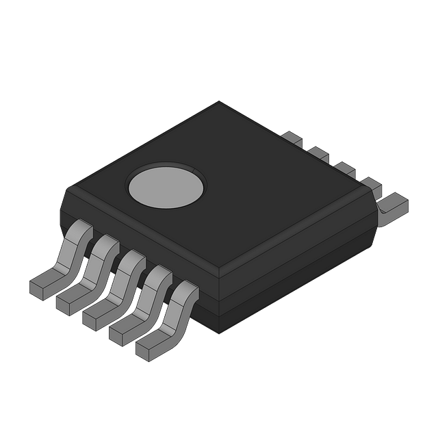
ICGOO电子元器件商城为您提供AD7153BRMZ由Analog设计生产,在icgoo商城现货销售,并且可以通过原厂、代理商等渠道进行代购。 AD7153BRMZ价格参考。AnalogAD7153BRMZ封装/规格:数据采集 - ADCs/DAC - 专用型, 电容数字转换器 12 b 串行 10-MSOP。您可以下载AD7153BRMZ参考资料、Datasheet数据手册功能说明书,资料中有AD7153BRMZ 详细功能的应用电路图电压和使用方法及教程。
AD7153BRMZ是Analog Devices Inc.(ADI)推出的一款专用型集成电路,属于数据采集系统中的ADC(模数转换器)类别。该器件是一款12位、多通道、低功耗的电容式触摸传感器接口,主要用于电容式感应应用,如触摸屏、触摸板和工业控制中的非接触式感应系统。

AD7153BRMZ的应用场景主要包括:

1. 消费电子产品:用于智能手机、平板电脑、笔记本电脑的触摸板和按钮检测,实现高灵敏度的电容变化检测,提升用户体验。

2. 工业控制:在工业人机界面(HMI)中用于触摸按钮、滑动条等电容式输入设备,具有抗干扰能力强、环境适应性好的特点。

3. 汽车电子:用于车载控制面板、中控台按钮、空调控制旋钮等电容式触摸控制,提升汽车内饰的美观性和可靠性。

4. 家电控制:应用于洗衣机、微波炉、电磁炉等家用电器的触摸控制面板,实现防水、防尘的非机械式操作。

该器件集成有自动校准功能,可适应环境变化,确保长期稳定性。其低功耗特性也适合电池供电设备使用。
| 参数 | 数值 |
| 产品目录 | 集成电路 (IC)半导体 |
| 描述 | IC CDC 12BIT 1/2CH 10MSOP模数转换器 - ADC 1-CH 12-bit CDC IC |
| 产品分类 | |
| 品牌 | Analog Devices |
| 产品手册 | |
| 产品图片 |
|
| rohs | 符合RoHS无铅 / 符合限制有害物质指令(RoHS)规范要求 |
| 产品系列 | 数据转换器IC,模数转换器 - ADC,Analog Devices AD7153BRMZ- |
| 数据手册 | |
| 产品型号 | AD7153BRMZ |
| 产品目录页面 | |
| 产品种类 | 模数转换器 - ADC |
| 供应商器件封装 | 10-MSOP |
| 分辨率 | 12 bit |
| 分辨率(位) | 12 b |
| 包装 | 管件 |
| 商标 | Analog Devices |
| 安装类型 | 表面贴装 |
| 安装风格 | SMD/SMT |
| 封装 | Tube |
| 封装/外壳 | 10-TFSOP,10-MSOP(0.118",3.00mm 宽) |
| 封装/箱体 | MSOP-10 |
| 工作温度 | -40°C ~ 85°C |
| 工作电源电压 | 2.7 V to 3.6 V |
| 工厂包装数量 | 50 |
| 接口类型 | Serial (2-Wire, I2C) |
| 数据接口 | 串行 |
| 最大功率耗散 | 432 uW |
| 最大工作温度 | + 85 C |
| 最小工作温度 | - 40 C |
| 标准包装 | 50 |
| 特色产品 | http://www.digikey.com/cn/zh/ph/analog-devices/ad715x.html |
| 电压-电源 | 2.7 V ~ 3.6 V |
| 电压源 | 单电源 |
| 类型 | 电容数字转换器 |
| 系列 | AD7153 |
| 结构 | Sigma-Delta |
| 转换速率 | 200 S/s |
| 输入类型 | Single-Ended/Differential |
| 通道数量 | 1 Channel |
| 采样率(每秒) | - |


- 商务部:美国ITC正式对集成电路等产品启动337调查
- 曝三星4nm工艺存在良率问题 高通将骁龙8 Gen1或转产台积电
- 太阳诱电将投资9.5亿元在常州建新厂生产MLCC 预计2023年完工
- 英特尔发布欧洲新工厂建设计划 深化IDM 2.0 战略
- 台积电先进制程称霸业界 有大客户加持明年业绩稳了
- 达到5530亿美元!SIA预计今年全球半导体销售额将创下新高
- 英特尔拟将自动驾驶子公司Mobileye上市 估值或超500亿美元
- 三星加码芯片和SET,合并消费电子和移动部门,撤换高东真等 CEO
- 三星电子宣布重大人事变动 还合并消费电子和移动部门
- 海关总署:前11个月进口集成电路产品价值2.52万亿元 增长14.8%


PDF Datasheet 数据手册内容提取
12-Bit Capacitance-to-Digital Converter Data Sheet AD7152/AD7153 FEATURES FUNCTIONAL BLOCK DIAGRAMS Capacitance-to-digital converters VDD Interfaces to floating sensors CAP+ AD7152 Resolution down to 0.25 fF (that is, up to 12 ENOB) CAP– CLOCK VOLTAGE GENERATOR REFERENCE Linearity: 0.05% CIN1(+) Common-mode (not changing) capacitance up to 5 pF CIN1(–) EXC1 12-BIT Σ-∆ I2C SDA Four capacitance ranges selectable per operation mode CIN2(+) MUX MODULATOR INTSEERRFIAALCE SCL ±0.25 pF to ±2 pF in differential mode CIN2(–) 0.5 pF to 4 pF in single-ended mode EXC2 TCoolnevrearnstio onf tpimarea spietirc c chaapnanceilt:a 5n mces ,t 2o0 g mrosu, n50d mups, taon 5d0 6 p0 Fm s EXCITATION DFIIGLTITEARL COCANLTIRBORLA TLIOOGNIC 07450-001 GND Internal clock oscillator Figure 1. 2-wire serial interface (I2C-compatible) VDD Power CAP+ AD7153 2.7 V to 3.6 V single-supply operation CAP– CLOCK VOLTAGE 100 μA current consumption GENERATOR REFERENCE Operating temperature: −40°C to +85°C CIN1(+) 10-lead MSOP 12-BIT Σ-∆ I2C SDA CIN1(–) MUX MODULATOR SERIAL APPLICATIONS EXC1 INTERFACE SCL AuPtroemssoutrivee m, ienadsuusrtermiael,n atn d medical systems for EXCITATION DFIIGLTITEARL COCANLTIRBORLA TLIOOGNIC 07450-002 Position sensing GND Level sensing Figure 2. Flowmeters Humidity sensing GENERAL DESCRIPTION The AD7152/AD7153 are 12-bit sigma-delta (Σ-Δ) capacitance-to- The AD7153 has one capacitance input channel, while the digital converters (CDCs). The capacitance to be measured is AD7152 has two channels. Each channel can be configured connected directly to the device inputs. The architecture features as single-ended or differential. The AD7152/AD7153 are inherent high resolution (12-bit no missing codes, up to 12-bit designed for floating capacitive sensors. effective resolution) and high linearity (±0.05%). The AD7152/ The AD7152/AD7153 have a 2-wire, I2C-compatible serial AD7153 have four capacitance input ranges per operation mode, interface. Both devices can operate with a single power supply ±0.25 pF to ±2 pF in differential mode and 0.5 pF to 4 pF in from 2.7 V to 3.6 V. They are specified over the temperature single-ended mode. range of −40°C to +85°C and are available in a 10-lead MSOP. The AD7152/AD7153 can accept up to 5 pF common-mode capacitance (not changing), which can be balanced by a programmable on-chip, digital-to-capacitance converter (CAPDAC). Rev. A Document Feedback Information furnished by Analog Devices is believed to be accurate and reliable. However, no responsibility is assumed by Analog Devices for its use, nor for any infringements of patents or other One Technology Way, P.O. Box 9106, Norwood, MA 02062-9106, U.S.A. rights of third parties that may result from its use. Specifications subject to change without notice. No license is granted by implication or otherwise under any patent or patent rights of Analog Devices. Tel: 781.329.4700 ©2008–2016 Analog Devices, Inc. All rights reserved. Trademarks and registered trademarks are the property of their respective owners. Technical Support www.analog.com
AD7152/AD7153 Data Sheet TABLE OF CONTENTS Features .............................................................................................. 1 Configuration Register .............................................................. 16 Applications ....................................................................................... 1 CAPDAC POS Register ............................................................. 17 Functional Block Diagrams ............................................................. 1 CAPDAC NEG Register ............................................................ 17 General Description ......................................................................... 1 Configuration2 Register ............................................................ 17 Revision History ............................................................................... 2 Circuit Description......................................................................... 18 Specifications ..................................................................................... 3 Capacitance-to-Digital Converter (CDC) .............................. 18 Timing Specifications .................................................................. 5 Excitation Source ........................................................................ 18 Absolute Maximum Ratings ............................................................ 6 CAPDAC ..................................................................................... 19 ESD Caution .................................................................................. 6 Single-Ended Capacitive Input ................................................. 19 Pin Configurations and Function Descriptions ........................... 7 Differential Capacitive Input .................................................... 20 Typical Performance Characteristics ............................................. 8 Parasitic Capacitance to Ground .............................................. 20 Serial Interface ................................................................................ 11 Parasitic Resistance to Ground ................................................. 20 Write Operation .......................................................................... 11 Parasitic Parallel Resistance ...................................................... 21 Read Operation ........................................................................... 11 Parasitic Serial Resistance ......................................................... 21 AD7152/AD7153 Reset .............................................................. 12 Input EMC Protection ............................................................... 21 General Call................................................................................. 12 Power Supply Decoupling and Filtering .................................. 21 Register Map .................................................................................... 13 Capacitive Gain Calibration ..................................................... 21 Status Register ............................................................................. 14 Capacitive System Offset Calibration ...................................... 21 Data Registers ............................................................................. 15 Typical Application Diagram .................................................... 22 Offset Calibration Registers ...................................................... 15 Outline Dimensions ....................................................................... 23 Gain Calibration Registers ........................................................ 15 Ordering Guide .......................................................................... 23 CAP Setup Registers .................................................................. 16 REVISION HISTORY 2/16—Rev. 0 to Rev. A Change to Address 0x01, Address 0x02 for Channel 1, Address 0x03, Address 0x04 (AD7152 Only) for Channel 2, 16 Bits, Read-Only, Default Value 0x0000 Section .................................. 15 Updated Outline Dimensions ....................................................... 23 5/08—Revision 0: Initial Version Rev. A | Page 2 of 24
Data Sheet AD7152/AD7153 SPECIFICATIONS V = 2.7 V to 3.6 V; GND = 0 V; −40°C to +85°C, unless otherwise noted. DD Table 1. Parameter Min Typ Max Unit1 Test Conditions/Comments CAPACITIVE INPUT Capacitive Input Ranges ±2 pF Differential mode ±1 pF ±0.5 pF ±0.25 pF 4 pF Single-ended mode 2 pF 1 pF 0.5 pF Gain Matching Between Ranges ±3 % of FS Integral Nonlinearity (INL)2 ±0.05 % of FS No Missing Codes2 12 Bits Resolution, p-p2, 3 10 Bits 25°C, V = 3.3 V, 4 pF range DD Resolution Effective2, 3 12 Bits 25°C, V = 3.3 V, 4 pF range DD Absolute Error4 ±20 fF 25°C, V = 3.3 V, after system offset DD calibration, ±2 pF range System Offset Calibration Range5, 6 40 % of FSR Offset Deviation over Temperature2 1 5 fF Single-ended mode, CIN and EXC pins disconnected, see Figure 8 0.3 1 fF Differential mode, CIN and EXC pins disconnected Gain Error7 0.5 % of FSR 25°C, V = 3.3 V DD Gain Deviation over Temperature2 0.3 0.4 % of FSR See Figure 7 Allowed Capacitance, CIN to GND2 50 pF See Figure 9 and Figure 10 Allowed Resistance, CIN to GND2 10 MΩ See Figure 13 Allowed Serial Resistance2 20 kΩ See Figure 16 Power Supply Rejection DC 2 fF/V See Figure 17 Normal-Mode Rejection2 −70 dB 50 Hz ± 1 Hz, conversion time = 60 ms −70 dB 60 Hz ± 1 Hz, conversion time = 50 ms Channel-to-Channel Isolation2 −70 dB AD7152 only CAPDAC Full Range 5 6.25 pF Resolution8 200 fF 5-bit CAPDAC Differential Nonlinearity (DNL)2 0.25 LSB See Figure 18 and Figure 19 Offset Deviation over Temperature2 0.3 % of CAPDAC FSR Single-ended mode EXCITATION Frequency 30.9 32 32.8 kHz Voltage ±V /2 V DD Allowed Capacitance, EXC to GND2 300 pF See Figure 11 and Figure 12 SERIAL INTERFACE LOGIC INPUTS (SCL, SDA) Input High Voltage, V 1.5 V IH Input Low Voltage, V 0.8 V IL Input Leakage Current (SCL) ±0.1 ±5 µA OPEN-DRAIN OUTPUT (SDA) Output Low Voltage, VOL 0.4 V ISINK = −6.0 mA Output High Leakage Current, I 0.1 5 µA V = V OH OUT DD POWER SUPPLY MONITOR Threshold Voltage, V 2.45 2.65 V DD Rev. A | Page 3 of 24
AD7152/AD7153 Data Sheet Parameter Min Typ Max Unit1 Test Conditions/Comments POWER REQUIREMENTS V -to-GND Voltage 2.7 3.6 V V = 3.3 V, nominal DD DD Current, I 9 100 120 µA DD Current Power-Down Mode, I 9 1 5 µA Temperature ≤ 25°C DD 3 10 µA Temperature = 85°C 1 Capacitance units: 1 pF = 10−12 F; 1 fF = 10−15 F; 1 aF = 10−18 F. 2 Specification is not production tested but is supported by characterization data at initial product release. 3 Except Channel 2 in differential mode. To achieve the specified performance in differential mode, the I2C interface must be idle during the capacitance conversion to prevent signal coupling from the SCL pin to the adjacent CIN2(−) pin. 4 Factory calibrated. The absolute error includes factory gain calibration error and integral nonlinearity error all at 25°C. At different temperatures, compensation for gain drift over temperature is required. 5 Specification is not production tested but guaranteed by design. 6 A system offset calibration is effectively a conversion; therefore, the offset error is of the order of the conversion noise. This applies after calibration at the temperature, capacitive input range, and applied VDD of interest. The capacitive input offset can be reduced using a system offset calibration. Large offsets should be removed using CAPDACs. 7 The gain error is factory calibrated at 25°C. At different temperatures, compensation for gain drift over temperature is required. 8 The CAPDAC resolution is five bits in the actual CAPDAC full range. Using the on-chip offset calibration or adjusting the capacitive offset calibration register can further reduce the CIN offset or the unchanging CIN component. 9 Digital inputs equal to VDD or GND. Rev. A | Page 4 of 24
Data Sheet AD7152/AD7153 TIMING SPECIFICATIONS V = 2.7 V to 3.6 V; GND = 0 V; Input Logic 0 = 0 V; Input Logic 1 = V ; −40°C to +85°C, unless otherwise noted. DD DD Table 2. Parameter Min Typ Max Unit Test Conditions/Comments SERIAL INTERFACE1, 2 See Figure 3. SCL Frequency 0 400 kHz SCL High Pulse Width, t 0.6 µs HIGH SCL Low Pulse Width, t 1.3 µs LOW SCL, SDA Rise Time, t 0.3 µs R SCL, SDA Fall Time, t 0.3 µs F Hold Time (Start Condition), t 0.6 µs After this period, the first clock is generated. HD;STA Set-Up Time (Start Condition), t 0.6 µs Relevant for repeated start condition. SU;STA Data Set-Up Time, t 0.1 µs SU;DAT Setup Time (Stop Condition), t 0.6 µs SU;STO Data Hold Time, t (Master) 0.01 µs HD;DAT Bus-Free Time (Between Stop and Start Conditions, t ) 1.3 µs BUF 1 Sample tested during initial release to ensure compliance. 2 All input signals are specified with input rise/fall times = 3 ns, measured between the 10% and 90% points. Timing reference points at 50% for inputs and outputs; output load = 10 pF. tLOW tR tF tHD;STA SCL tHD;STA tHD;DAT tHIGH tSU;DAT tSU;STA tSU;STO SDA PtBUF S S P 07450-003 Figure 3. Serial Interface Timing Diagram Rev. A | Page 5 of 24
AD7152/AD7153 Data Sheet ABSOLUTE MAXIMUM RATINGS Stresses at or above those listed under Absolute Maximum T = 25°C, unless otherwise noted. A Ratings may cause permanent damage to the product. This is a Table 3. stress rating only; functional operation of the product at these Parameter Rating or any other conditions above those indicated in the operational Positive Supply Voltage, V to GND −0.3 V to +3.9 V section of this specification is not implied. Operation beyond DD Voltage on Any Input or Output Pin to GND −0.3 V to V + 0.3 V the maximum operating conditions for extended periods may DD ESD Rating (ESD Association Human 4 kV affect product reliability. Body Model, S5.1) ESD CAUTION ESD Rating (Field-Induced Charged 750 V Device Model) Operating Temperature Range −40°C to +85°C Storage Temperature Range −65°C to +150°C Junction Temperature 150°C MSOP θ Thermal Impedance-to-Air 206°C/W JA θ Thermal Impedance-to-Case 44°C/W JC Reflow Soldering (Pb-Free) Peak Temperature 260 (+0/−5)°C Time at Peak Temperature 10 sec to 40 sec Rev. A | Page 6 of 24
Data Sheet AD7152/AD7153 PIN CONFIGURATIONS AND FUNCTION DESCRIPTIONS GND 1 10 SDA GND 1 10 SDA VDD 2 AD7153 9 SCL VDD 2 AD7152 9 SCL CIN1(–) 3 TOP VIEW 8 NC CIN1(–) 3 TOP VIEW 8 CIN2(–) CIN1(+) 4 (Not to Scale) 7 NC CIENX1(C+2) 45 (Not to Scale) 76 CEXINC21(+) 07450-004 NC 5NC = NO CONNECT6 EXC1 07450-005 Figure 4. AD7152 Pin Configuration Figure 5. AD7153 Pin Configuration Table 4. Pin Function Descriptions Pin No. Mnemonic Description 1 GND Ground Pin. 2 VDD Power Supply Voltage. This pin should be decoupled to GND, using a low impedance capacitor, for example, in combination with a 10 μF tantalum and a 0.1 μF multilayer ceramic capacitor. 3 CIN1(–) CDC Negative Capacitive Input of Channel 1. If not used, this pin can be left as an open circuit or connected to GND. This pin is internally disconnected in single-ended CDC configuration. 4 CIN1(+) CDC Positive Capacitive Input of Channel 1. If not used, this pin can be left as an open circuit or connected to GND. 5 EXC2/NC AD7152: CDC Excitation Output for Channel 2. The measured capacitance is connected between one of the EXC pins and one of the CIN pins. If not used, these pins should be left as an open circuit. AD7153: No Connect. This pin must be left as an open circuit. 6 EXC1 CDC Excitation Output for Channel 1. The measured capacitance is connected between one of the EXC pins and one of the CIN pins. If not used, these pins should be left as an open circuit. 7 CIN2(+)/NC AD7152: CDC Positive Capacitive Input of Channel 2. If not used, this pin can be left as an open circuit or connected to GND. AD7153: No Connect. This pin must be left as an open circuit. 8 CIN2(–)/NC AD7152: CDC Negative Capacitive Input of Channel 2. If not used, this pin can be left as an open circuit or connected to GND. This pin is internally disconnected in single-ended CDC configuration. AD7153: No Connect. This pin must be left as an open circuit. 9 SCL Serial Interface Clock Input. Connects to the master clock line. Requires a pull-up resistor if one is not already provided in the system. 10 SDA Serial Interface Bidirectional Data. Connects to the master data line. Requires a pull-up resistor if one is not provided elsewhere in the system. Rev. A | Page 7 of 24
AD7152/AD7153 Data Sheet TYPICAL PERFORMANCE CHARACTERISTICS 0.05 2 0.04 0 0.03 0.02 R) –2 R) FS 9pF 3pF S0.01 % % of F 0 ROR ( –4 INL (0.01 AIN ER –6 0.02 G –8 0.03 –10 0.04 0.05–2 –1 CAPACIT0ANCE (pF) 1 2 07450-106 –120 50 100CAPL1O5A0DTO2G00ND(pF)250 300 350 07450-109 Figure 6. Capacitance Input Integral Nonlinearity, Figure 9. Capacitance Input Error vs. Capacitance Between CIN and GND; VDD = 3.3 V, See Figure 34 Single-Ended Mode, CIN(+) to EXC = 3 pF and 9 pF, VDD = 3.3 V 0.20 2 TC ≈ 28ppm/°C 2pF 0.15 0 0.10 %FSR) 0.05 %FSR) –2 8pF R ( 0.00 R ( –4 O O N ERR–0.05 N ERR –6 AI–0.10 AI G G –8 –0.15 –10 –0.20 –0.2550 25 0TEMPERA2T5URE (°C)50 75 100 07450-107 –120 50 10C0AP LO1A50D TO G2N0D0 (pF)250 300 350 07450-110 Figure 7. Capacitance Input Gain Drift vs. Temperature, Figure 10. Capacitance Input Error vs. Capacitance Between CIN and GND, VDD = 3.3 V, Range = ±2 pF Differential Mode, CIN(+) to EXC = 2 pF and 8 pF, CIN(−) to EXC = 0 pF and 6 pF, VDD = 3.3 V 0.4 0.3 0.2 0.2 E (fF) SR) 0.1 NC %F TA R ( CAPACI 0 N ERRO 0 T AI–0.1 E G S F–0.2 F O –0.2 –0.4–50 –25 T0EMPERA2T5URE (°C)50 75 100 07450-108 –0.30 50 100CAP LO15A0D TO G20N0D (pF)250 300 350 07450-111 Figure 8. Capacitance Input Offset Drift vs. Temperature, Figure 11. Capacitance Input Error vs. Capacitance Between EXC and GND, VDD = 3.3 V, CIN and EXC Pins Open Circuit Single-Ended Mode, CIN(+) to EXC = 9 pF, VDD = 3.3 V Rev. A | Page 8 of 24
Data Sheet AD7152/AD7153 0.3 10 0.2 0 %FSR) 0.1 %FSR) –10 GAIN ERROR (–0.10 GAIN ERROR ( ––3200 –0.2 –40 –0.30 50 100CAP L1O5A0D TO 2G0N0D (pF)250 300 350 07450-112 –501 PAR1A0LLEL RESISTANCE1 0(0MΩ) 100007450-115 Figure 12. Capacitance Input Error vs. Capacitance Between EXC and GND, Figure 15. Capacitance Input Error vs. Parasitic Parallel Resistance Differential Mode, CIN(+) to EXC = 8 pF, Single-Ended Mode, CIN(+) to EXC = 9 pF, VDD = 3.3 V CIN(−) to EXC = 6 pF, VDD = 3.3 V 2 0 3pF 0 –5 SR)–2 SR)–10 %F %F 9pF R ( R ( RO–4 RO–15 R R E E N N GAI–6 GAI–20 –8 –25 –101 RESIST1A0NCE CIN TO GROU1N00D (MΩ) 100007450-113 –300 20 SERIA4L0 RESISTAN6C0E (kΩ) 80 10007450-116 Figure 13. Capacitance Input Error vs. Parasitic Resistance CIN to GND, Figure 16. Capacitance Input Error vs. Serial Resistance, Single-Ended Mode, CIN(+) to EXC = 9 pF, VDD = 3.3 V Single-Ended Mode, CIN(+) to EXC = 3 pF and 9 pF, VDD = 3.3 V 0.6 0.2 0.4 0.0 %FSR) 0.2 OR (fF) –0.2 R ( RR ERRO 0 AIN E –0.4 N G AI –0.2 –0.6 G –0.4 –0.8 –0.61 RESIST1A0NCE EXC TO GROU10N0D (MΩ) 100007450-114 –1.02.6 2.8 3.0 VD3D.2 (V) 3.4 3.6 3.8 07450-117 Figure 14. Capacitance Input Error vs. Parasitic Resistance EXC to GND, Figure 17. Capacitance Input Power Supply Rejection (PSR), Single-Ended Mode, CIN(+) to EXC = 9 pF, VDD = 3.3 V Differential Mode; CIN(+) to EXC = 1.9 pF Rev. A | Page 9 of 24
AD7152/AD7153 Data Sheet 30 0 20 –20 10 B) d NL (fF) 0 R GAIN (–40 D E T L –10 FI –60 –20 –300 5 10CAPDA1C5 CODE 20 25 30 07450-118 –800 INPU5T0 SIGNAL FREQUEN1C0Y0 (Hz) 15007450-120 Figure 18. CAPDAC(+) Differential Nonlinearity (DNL) Figure 20. Capacitance Channel Frequency Response, Conversion Time = 60 ms 30 0 20 –20 10 B) d NL (fF) 0 R GAIN (–40 D E T L –10 FI –60 –20 –300 5 10CAPDA1C5 CODE 20 25 30 07450-119 –800 INPU5T0 SIGNAL FREQUEN1C0Y0 (Hz) 15007450-221 Figure 19. CAPDAC(−) Differential Nonlinearity (DNL) Figure 21. Capacitance Channel Frequency Response, Conversion Time = 50 ms Rev. A | Page 10 of 24
Data Sheet AD7152/AD7153 SERIAL INTERFACE A stop condition is defined by a low-to-high transition on SDA The AD7152/AD7153 support an I2C-compatible, 2-wire serial while SCL remains high. If a stop condition is ever encountered interface. The two wires on the I2C bus are called SCL (clock) by the AD7152/AD7153, it returns to its idle condition and the and SDA (data). These two wires carry all addressing, control, address pointer is reset to Address 0x00. and data information one bit at a time over the bus to all connected peripheral devices. The SDA wire carries the data, while the If a data byte is transmitted after the register address pointer SCL wire synchronizes the sender and receiver during the byte, the AD7152/AD7153 load this byte into the register that data transfer. I2C devices are classified as either master or slave is currently addressed by the address pointer register. The devices devices. A device that initiates a data transfer message is called a send an acknowledge and the address pointer autoincrementer master; a device that responds to this message is called a slave. automatically increments the address pointer register to the next internal register address. Thus, subsequent transmitted To control the AD7152/AD7153 via the bus, the following data bytes are loaded into sequentially incremented addresses. protocol must be followed. The master initiates a data transfer by establishing a start condition, defined by a high-to-low If a repeated start condition is encountered after the address transition on SDA while SCL remains high. This indicates that pointer byte, all peripherals connected to the bus respond the start byte follows. This 8-bit start byte is made up of a 7-bit exactly as previously outlined for a start condition, that is, a address plus an R/W bit indicator. repeated start condition is treated the same as a start condition. When a master device issues a stop condition, it relinquishes All peripherals connected to the bus respond to the start control of the bus, allowing another master device to take condition and shift in the next 8 bits (7-bit address and an control. Hence, a master wanting to retain control of the bus R/W bit). The bits arrive MSB first. The peripheral that issues successive start conditions known as repeated start recognizes the transmitted address responds by pulling the conditions. data line low during the ninth clock pulse. This is known as the acknowledge bit. All other devices withdraw from the bus at READ OPERATION this point and maintain an idle condition. An exception to this When a read is selected in the start byte, the register that is is the general call address, which is described in the General currently addressed by the address pointer is transmitted onto Call section. The idle condition is where the device monitors the SDA line by the AD7152/AD7153. The regulator is then the SDA and SCL lines waiting for the start condition and the clocked out by the master device, and the AD7152/AD7153 correct address byte. The R/W bit determines the direction of await an acknowledge from the master. the data transfer. A Logic 0 LSB in the start byte means that the If an acknowledge is received from the master, the address master writes information to the addressed peripheral. In this autoincrementer automatically increments the address pointer case, the device becomes a slave receiver. A Logic 1 LSB in the register and outputs the next addressed register content onto start byte means that the master reads information from the the SDA line for transmission to the master. If no acknowledge addressed peripheral. In this case, the device becomes a slave is received, the AD7152/AD7153 return to the idle state and the transmitter. In all instances, the AD7152/AD7153 act as a standard slave device on the I2C bus. address pointer is not incremented. The autoincrementer of the address pointers allows block data The start byte address is Address 0x90 for a write and to be written or read from the starting address and subsequent Address 0x91 for a read. incremental addresses. WRITE OPERATION In continuous conversion mode, the autoincrementer of the When a write is selected, the byte following the start byte is address pointers should be used for reading a conversion result; always the register address pointer (subaddress) byte, which that is, the three data bytes should be read using one multibyte points to one of the internal registers on the AD7152/AD7153. read transaction rather than three separate single-byte The address pointer byte is automatically loaded into the transactions. The single-byte data read transaction may result in address pointer register and acknowledged by the AD7152/ the data bytes from two different results being mixed. AD7153. After the address pointer byte acknowledge, a stop condition, a repeated start condition, or another data byte can follow from the master. Rev. A | Page 11 of 24
AD7152/AD7153 Data Sheet The user can also access any unique register (address) on a AD7152/AD7153 RESET one-to-one basis without having to update all the registers. To reset the AD7152/AD7153 without having to reset the entire However, the address pointer register contents cannot be read. I2C bus, an explicit reset command is provided. This command If an incorrect address pointer location is accessed, or if the user uses a particular address pointer word as a command word to allows the autoincrementer to exceed the required register reset the device and upload all default settings. The AD7152/ address, apply the following requirements: AD7153 do not respond to the I2C bus commands (no acknowl- edge) during the default values upload for approximately 150 μs In read mode, the AD7152/AD7153 continue to output (maximum 200 μs). various internal register contents until the master device issues a no acknowledge, start, or stop condition. The The reset command address word is 0xBF. contents of the address pointers autoincrementer are reset GENERAL CALL to point to the status register at Address 0x00 when a stop When a master issues a slave address consisting of seven 0s with condition is received at the end of a read operation. This the eighth bit (R/W bit) set to 0, this is called the general call allows the status register to be read (polled) continually address. The general call address is for addressing every device without having to constantly write to the address pointer. connected to the I2C bus. The AD7152/AD7153 acknowledge In write mode, the data for the invalid address is not this address and read the following data byte. loaded into the registers of the AD7152/AD7153, but an acknowledge is issued by the AD7152/AD7153. If the second byte is 0x06, the AD7152/AD7153 are reset, completely uploading all default values. The AD7152/AD7153 do not respond to the I2C bus commands (no acknowledge) during the default values upload for approximately 150 μs (maximum 200 μs). The AD7152/AD7153 do not acknowledge any other general call commands. SDA SCL STASRT A1D toD R7 R8/W AC9K SUBA1 DtoD 7RESS 8 A9CK 1D AtoT A7 8 AC9K STPOP 07450-006 Figure 22. Bus Data Transfer WRITE S SLAVEADDR A(S) SUBADDR A(S) DATA A(S) DATA A(S) P SEQUENCE LSB = 0 LSB = 1 READ S SLAVEADDR A(S) SUBADDR A(S) S SLAVEADDR A(S) DATA A(M) DATA A(M) P SEQUENCE 07450-007 Figure 23. Write and Read Sequences Table 5. I2C Abbreviation Abbreviation Definition S Start bit P Stop bit A(S) Acknowledge by slave A(M) Acknowledge by master A(S) No acknowledge by slave A(M) No acknowledge by master ACK Acknowledge R/W Read/write Rev. A | Page 12 of 24
Data Sheet AD7152/AD7153 REGISTER MAP The master can write to or read from all of the registers except read/write operation is selected, the address pointer register is the address pointer register, which is a write-only register. The set up. The address pointer register determines from or to which address pointer register determines which register the next read register the operation takes place. A read/write operation is or write operation accesses. All communications with the device performed from/to the target address, which then increments to through the bus start with an access to the address pointer the next address until a stop command on the bus is performed. register. After the device has been accessed over the bus and a Table 6. Register Summary Subaddress Default Register Name Dec Hex Access Bit 7 Bit 6 Bit 5 Bit 4 Bit 3 Bit 2 Bit 1 Bit 0 Value Status 0 0x00 R PWDN Unused Unused Unused Unused C1C2 RDY2 RDY1 0x03 Channel 1 Data MSB 1 0x01 R Channel 1 data, high byte 0x00 Channel 1 Data LSB 2 0x02 R Channel 1 data, low byte 0x00 Channel 2 Data MSB1 3 0x03 R Channel 2 data, high byte 0x00 Channel 2 Data LSB 4 0x04 R Channel 2 data, low byte 0x00 Channel 1 Offset MSB 5 0x05 R/W Channel 1 offset calibration coefficient, high byte 0x80 Channel 1 Offset LSB 6 0x06 R/W Channel 1 offset calibration coefficient, low byte 0x00 Channel 2 Offset MSB1 7 0x07 R/W Channel 2 offset calibration coefficient, high byte 0x80 Channel 2 Offset LSB1 8 0x08 R/W Channel 2 offset calibration coefficient, low byte 0x00 Channel 1 Gain MSB 9 0x09 R/W Channel 1 gain coefficient, high byte, factory calibrated 0xXX Channel 1 Gain LSB 10 0x0A R/W Channel 1 gain coefficient, low byte, factory calibrated 0xXX Channel 1 Setup 11 0x0B R/W Range 1 Range 0 CAPDIFF Unused Unused 0x00 Channel 2 Gain MSB1 12 0x0C R/W Channel 2 gain coefficient, high byte, factory calibrated 0xXX Channel 2 Gain LSB1 13 0x0D R/W Channel 2 gain coefficient, low byte, factory calibrated 0xXX Channel 2 Setup1 14 0x0E R/W Range 1 Range 0 CAPDIFF Unused Unused 0x00 Configuration 15 0x0F R/W Unused Unused Unused Ch1en Ch2en MD2 MD1 MD0 0x00 Reserved 16 0x10 R/W Unused 0x00 CAPDAC POS 17 0x11 R/W DACPen Unused Unused DACP Bits[4:0] value 0x00 CAPDAC NEG 18 0x12 R/W DACNen Unused Unused DACN Bits[4:0] value 0x00 Configuration2 26 0x1A R/W Unused Unused OSR1 OSR0 Unused Unused Unused Unused 0x00 1 AD7152 only. Rev. A | Page 13 of 24
AD7152/AD7153 Data Sheet STATUS REGISTER Address 0x00 Read Only Default Value 0x03 This register indicates the status of the converter. The status register can be read via the 2-wire serial interface to query a finished conversion. Table 7. Status Register Bit Map Bit Bit 7 Bit 6 Bit 5 Bit 4 Bit 3 Bit 2 Bit 1 Bit 0 Mnemonic PWDN Unused Unused Unused Unused C1C2 RDY2 RDY1 Default 0 0 0 0 0 0 1 1 Table 8. Status Register Bit Descriptions Bit Mnemonic Description 7 PWDN PWDN = 1 indicates that the V voltage level is below 2.45 V typically or the device is in power-down mode DD 6 to 3 N/A Not used, always read 0 2 C1C2 C1C2 = 0 indicates that the last conversion performed was from Channel 1, C1C2 = 1 indicates that the last conversion performed was from Channel 2 1 RDY2 RDY2 = 0 indicates that a conversion on the Channel 2 has been finished and new unread data is available (AD7152 only) 0 RDY1 RDY1 = 0 indicates that a conversion on the Channel 1 has been finished and new unread data is available Rev. A | Page 14 of 24
Data Sheet AD7152/AD7153 DATA REGISTERS Therefore, to prevent incorrect data reading through the Address 0x01, Address 0x02 for Channel 1, serial interface, the two bytes of a data register should be Address 0x03, Address 0x04 (AD7152 Only) for Channel 2, read sequentially using the register address pointer auto- 16 Bits, Read-Only, Default Value 0x0000 increment feature of the serial interface. Data from the last complete capacitance-to-digital conversion OFFSET CALIBRATION REGISTERS reflects the capacitance on the input. Only the 12 MSBs of the Address 0x05, Address 0x06 for Channel 1, data registers are used for the CDC result. The 4 LSBs are Address 0x07, Address 0x08 for Channel 2 (AD7152 Only) always 0, as shown in Figure 24. 16 Bits Read/Write, Default Value 0x8000 MSB DATA HIGH DATA LOW LSB The offset calibration registers hold the zero-scale calibration BIT 7BIT 6BIT 5BIT 4BIT 3BIT 2BIT 1BIT 0 BIT 7BIT 6BIT 5BIT 4BIT 3BIT 2BIT 1BIT 0 coefficients. 12-BIT CDC RESULT 0 07450-044 The zero-scale calibration coefficient digitally maps the zero Figure 24. CDC Data Register capacitance on the CDC input to the zero-scale data code. The coefficient can be used for compensation of the AD7152/ The AD7152/AD7153 are factory gain calibrated and map the AD7153 internal offset as well as the system level offset within CDC full-scale raw data range of 0x3000 to 0xCFF0 to a CDC specified offset calibration limits. full-scale data register range of 0x0000 to 0xFFF0 (see Table 9). Users can set the coefficient by executing the offset calibration Table 9. AD7152/AD7153 Capacitance-to-Data Mapping after connecting the zero-scale capacitance to the system input. Input Capacitance (4 pF range) Alternatively, the coefficient value can be written to the offset Data Reg Differential Mode Single-Ended Mode calibration register(s) by the host software, for example, values 0x0000 Negative full scale (–2 pF) Zero scale (0 pF) stored in a host nonvolatile memory. 0x8000 Zero scale (0 pF) Midscale (2 pF) Note that there is a difference between code mapping in differ- 0xFFF0 Positive full scale (+2 pF) Full scale (4 pF) ential and single-ended input mode. In differential mode, the The data register output in differential mode is internally nominal zero-scale calibration coefficient value is a power-on calculated using the following equation: default, 0x8000. In single–ended mode, the nominal zero-scale Data Reg = (Code – (Offset Reg – 0x8000)) × Gain + 0x8000 (1) calibration coefficient value is 0x3000. The input capacitance can be calculated from the output data The difference means that before using the single-ended mode using the following equation: (or any time when changing between modes afterwards), the user should either perform offset calibration with capacitance DataReg −0x8000 C(pF)= ×InputRange (2) close to 0 pF connected to the input or write the offset calibra- 0xFFF0 tion register(s) value(s) close to 0x8000 for differential mode or The data register output in single-ended mode is internally value close to 0x3000 for single-ended mode. calculated using the following equation: On the AD7152, the two capacitive channels have individual Data Reg = (Code − (Offset Reg − 0x3000)) × Gain (3) offset registers and each channel can be calibrated individually. The input capacitance can be calculated from the output data GAIN CALIBRATION REGISTERS using the following equation: Address 0x09, Address 0x0A for Channel 1 DataReg Address 0x0C, Address 0x0D for Channel 2 (AD7152 Only) C(pF)= ×InputRange (4) 16 Bits Read/Write, Default Value 0xXXXX 0xFFF0 The capacitive gain calibration registers hold the capacitive where Input Range = 4 pF, 2 pF, 1 pF, or 0.5 pF. channel full-scale factory calibration coefficient. The gain A data register is updated after a finished conversion on the calibration factor can be calculated using the following capacitive channel, with one exception: when the serial interface equation: read operation from the data register is in progress, the data register is not updated and the new capacitance conversion 216 +GainReg Gain= (5) result is lost. 216 The stop condition on the serial interface is considered to be the On the AD7152, the two capacitive channels each have a gain end of the read operation. register, which allows the device to gain calibrate each channel individually. Rev. A | Page 15 of 24
AD7152/AD7153 Data Sheet CAP SETUP REGISTERS Address 0x0B for Channel 1 Address 0x0E Channel 2 (AD7152 Only) Default Value 0x00 Table 10. CAP Setup Register Bit Map Bit Bit 7 Bit 6 Bit 5 Bit 4 Bit 3 Bit 2 Bit 1 Bit 0 Mnemonic Range 1 Range 0 CAPDIFF Unused Unused Unused Unused Unused Default 0 0 0 0 0 0 0 0 Table 11. CAP Setup Register Bit Descriptions Bit Mnemonic Description 7 Range 1 Capacitive input range and mode setup 6 Range 0 Capacitive Input Range 5 CAPDIFF Range 1 Range 0 CAPDIFF = 1 (Differential Mode) CAPDIFF = 0 (Single-Ended Mode) 0 0 ±1 pF 2 pF 0 1 ±0.25 pF 0.5 pF 1 0 ±0.5 pF 0.25 pF 1 1 ±2 pF 4 pF 4 to 0 N/A These bits must be 0 for proper operation CONFIGURATION REGISTER Address Pointer 0x0F Default Value 0x00 Table 12. Configuration Register Bit Map Bit Bit 7 Bit 6 Bit 5 Bit 4 Bit 3 Bit 2 Bit 1 Bit 0 Mnemonic Unused Unused Unused Ch1en Ch2en MD2 MD1 MD0 Default 0 0 0 0 0 0 0 0 Table 13. Configuration Register Bit Descriptions Bit Mnemonic Description 7 to 5 N/A These bits must be 0 for proper operation 4 Ch1en Ch2en = 1 enables Channel 1 for single conversion, continuous conversion, or calibration 3 Ch2en Ch2en = 1 enables Channel 2 for single conversion, continuous conversion, or calibration 2 MD2 Converter mode of operation setup 1 MD1 MD2 MD1 MD0 Mode 0 MD0 0 0 0 Idle 0 0 1 Continuous conversion 0 1 0 Single conversion 0 1 1 Power-down 1 0 0 N/A 1 0 1 Capacitance system offset calibration 1 1 0 Capacitance system gain calibration 1 1 1 N/A Rev. A | Page 16 of 24
Data Sheet AD7152/AD7153 CAPDAC POS REGISTER Address 0x11 Default Value 0x00 Table 14. Status Register Bit Map Bit Bit 7 Bit 6 Bit 5 Bit 4 Bit 3 Bit 2 Bit 1 Bit 0 Mnemonic DACPen Unused Unused DACP – Bits[4:0] Value Default 0 0 0 0x00 Table 15. Status Register Bit Descriptions Bit Mnemonic Description 7 DACPen DACPen = 1 connects the capacitive DAC POS to the positive capacitive input 6 to 5 N/A These bits must be 0 for proper operation 4 to 0 DACP DACP value, Code 0x00 = 0 pF, Code 0x1F = full range CAPDAC NEG REGISTER Address 0x12 Default Value 0x00 Table 16. Status Register Bit Map Bit Bit 7 Bit 6 Bit 5 Bit 4 Bit 3 Bit 2 Bit 1 Bit 0 Mnemonic DACNen Unused Unused DACN – Bit[4:0] Value Default 0 0 0 0x00 Table 17. Status Register Bit Descriptions Bit Mnemonic Description 7 DACNen DACNen = 1 connects the capacitive DAC NEG to the positive capacitive input 6 to 5 N/A These bits must be 0 for proper operation 4 to 0 DACN DACN value, Code 0x00 = 0 pF, Code 0x1F = full range CONFIGURATION2 REGISTER Address 0x1A, Default Value 0x00 Table 18. Configuration2 Register Bit Map Bit Bit 7 Bit 6 Bit 5 Bit 4 Bit 3 Bit 2 Bit 1 Bit 0 Mnemonic Unused Unused OSR1 OSR0 Default 0 0 0 0 0 0 0 0 Table 19. Configuration2 Register Bit Descriptions Bit Mnemonic Description 7 to 6 N/A These bits must be 0 for proper operation 5 OSR1 Capacitive channel digital filter setup; conversion time/update rate setup per channel 4 OSR0 OSR1 OSR0 Conversion Time (ms) Update Rate (Hz) 0 0 5 200 0 1 20 50 1 0 50 20 1 1 60 16.7 3 to 0 N/A These bits must be 0 for proper operation Rev. A | Page 17 of 24
AD7152/AD7153 Data Sheet CIRCUIT DESCRIPTION VDD CAPACITANCE-TO-DIGITAL CONVERTER (CDC) CAP+ AD7152 Figure 27 shows the CDC simplified functional diagram. The CAP– CLOCK VOLTAGE measured capacitance CX is connected between the excitation GENERATOR REFERENCE source and the Σ-Δ modulator input. A square-wave excitation CIN1(+) signal is applied on the C during the conversion and the mod- CIN1(–) X EXC1 12-BIT Σ-∆ I2C SDA ulator continuously samples the charge going through the CX. CIN2(+) MUX MODULATOR INTSEERRFIAALCE SCL The digital filter processes the modulator output, which is a CIN2(–) stream of 0s and 1s containing the information in 0 and 1 EXC2 density. The data from the digital filter is scaled, applying the EXCITATION DFIIGLTITEARL COCANLTIRBORLA TLIOOGNIC 07450-025 cthaeli bseraritaiol nin ctoereffafcicei.e Tnthse, aAnDd7 t1h5e2 f/iAnDal7 r1e5s3u lat rcea dne bsieg rneeadd ftohrr ough GND floating capacitive sensors. Therefore, both C plates have to Figure 25. AD7152 Block Diagram X be isolated from ground. VDD CAPACITANCE-TO-DIGITAL CONVERTER CAP+ AD7153 (CDC) CAP– CLOCK VOLTAGE CLOCK GENERATOR REFERENCE GENERATOR CIN1(+) DATA CIN1(–) MUX M1O2D-BUILTA ΣT-O∆R SEIR2CIAL SDA CIN M1O2D-BUILTA ΣT-O∆R DFIIGLTITEARL EXC1 INTERFACE SCL CX EXC EXCITATION EXCITATION DFIIGLTITEARL COCANLTIRBORLA TLIOOGNIC 07450-026 Figure 27. CDC Simplified Block Diagram 07450-027 GND EXCITATION SOURCE Figure 26. AD7153 Block Diagram The core of the AD7152/AD7153 is a precision converter The AD7152/AD7153 have one excitation source. For the consisting of a second-order modulator (Σ-Δ or charge- AD7152, the excitation source is switched between the balancing) and a third-order digital filter. excitation pins, EXC1 and EXC2, depending on which channel performs a conversion. In addition to the converter, the AD7152/AD7153 integrate a multiplexer, an excitation source, and CAPDACs for the capaci- tive inputs, a voltage reference, a complete clock generator, a control and calibration logic, and an I2C-compatible serial interface. The AD7153 has one capacitive input, while the AD7152 has two capacitive inputs. For the AD7152, the modulator input and the excitation source are multiplexed between the converting channel. All other features and specifications are identical for both devices. Rev. A | Page 18 of 24
Data Sheet AD7152/AD7153 CAPDAC SINGLE-ENDED CAPACITIVE INPUT The CDC full-scale input range of the AD7152/AD7153 can When configured for a single-ended mode (the CAPDIFF bit in be set to ±0.25 pF, ±0.5 pF, ± 1 pF, and ±2 pF in differential the Channel 1 Setup or Channel 2 Setup registers is set to 0), the mode or 0.5 pF, 1 pF, 2 pF, and 4 pF in single-ended mode. AD7152/AD7153 CIN(−) pin is disconnected internally. The For simplicity, the following text and figures use the maximum CDC (without using the CAPDACs) can measure positive input full scale of ±2 pF and +4 pF. capacitance in the range of 0 pF to 4 pF (see Figure 29). The devices can accept a higher capacitance on the input and the common-mode or offset capacitance (unchanging component) CAPDAC(+) can be balanced by programmable on-chip CAPDACs. OFF CIN(+) 0x0000 ... 0xFFF0 DATA CAPDIFF = 0 0pFTO 4pF CAPDAC(+) CIN(–) CDC CIN(+) CAPDAC(–) CDC DATA CX OFF CIN(–) 0pFTO 4pF CX CY CAPDAC(–) EXC 07450-024 Figure 29. CDC Single-Ended Input Mode EXC 07450-010 Tinhpeu Ct rAaPngDeA. C can be used for programmable shifting of the Figure 28. Using a CAPDAC Figure 30 shows how to shift the input range up to 9 pF absolute The CAPDAC can be understood as a negative capacitance value of capacitance connected to the CIN(+) using connected internally to the CIN pin. There are two independent the CAPDAC(+) only. CAPDACs, one connected to the CIN(+) and the second connected to the CIN(–). CAPDAC(+) In differential mode, the relationship between the capacitance 5pF input and output data can be expressed as CIN(+) 0x0000 ... 0xFFF0 DATA CAPDIFF = 0 0pFTO 4pF DATA ≈ (CX − CAPDAC(+)) − (CY − CAPDAC(−)) CIN(–) CDC In single-ended mode, the relationship between the capacitance input and output data can be expressed as CAPDAC(–) CX OFF 5pFTO 9pF DATA ≈ C −(CAPDAC(+) + CAPDAC(−)) X Tfuhnec CtioAnP, DarAeC wse hlla mvea tac 5h-ebdi tt ore esaocluht iootnh eera, cahn,d m hoanvoe tao ndiecf itnreadn sfer EXC 07450-124 Figure 30. Using CAPDAC in Single-Ended Mode temperature coefficient. The CAPDAC full range (absolute value) is not factory calibrated and can vary up to ±20% with Figure 31 shows how to shift the input range up to 14 pF the manufacturing process (see the Specifications section, absolute value of capacitance connected to the CIN(+) using Figure 18, and Figure 19). both CAPDAC(+) and CAPDAC(−). The CAPDACs are shared by the two capacitive channels on the AD7152. If the CAPDACs need to be set individually, the host CAPDAC(+) 5pF controller software should reload the CAPDAC values to the CIN(+) 0x0000 ... 0xFFF0 AD7152 before executing a conversion on a different channel. DATA CAPDIFF = 0 0pFTO 4pF CIN(–) CDC CAPDAC(–) CX 5pF 10pFTO 14pF EXC 07450-224 Figure 31. Using CAPDAC in Single-Ended Mode Rev. A | Page 19 of 24
AD7152/AD7153 Data Sheet DIFFERENTIAL CAPACITIVE INPUT PARASITIC CAPACITANCE TO GROUND When configured for differential mode (the CAPDIFF bit in the Channel 1 Setup or Channel 2 Setup registers is set to 1), the CDC measures the difference between positive and negative capacitance input. CGND1 CIN CDC DATA Each of the two input capacitances, C and C , between the X Y EXC and CIN pins must be less than 2 pF (without using the CAPDACs) or must be less than 9 pF and balanced by the CX CAPDACs. Balancing by the CAPDACs means that both ICf Xt h−e C uAnbPaDlaAnCce(+d) c aanpdac CitYa n−c Ce AbePtDwAeeCn( −th)e a EreX lCes as nthda CnI 2N p pFi.n s CGND2 EXC 07450-012 is higher than 2 pF, the CDC introduces a gain error, an offset Figure 35. Parasitic Capacitance to Ground error, and nonlinearity error (see Figure 32, Figure 33, and The CDC architecture used in the AD7152/AD7153 measures Figure 34). C connected between the EXC pin and the CIN pin. In theory, X any capacitance, C , to ground should not affect the CDC GND CAPDAC(+) result (see Figure 35). OFF CIN(+) 0x0000 ... 0xFFF0 The practical implementation of the circuitry in the chip DATA ±2pF implies certain limits and the result is gradually affected by CIN(–) CAPDIFF = 1 CDC capacitance to ground. See the allowed capacitance to GND in the Specifications table and, Figure 9 through Figure 12. CAPDAC(–) OFF PARASITIC RESISTANCE TO GROUND CX CY 0pFTO 4pF 0pFTO 4pF EXC 07450-020 Figure 32. CDC Differential Input Mode RGND1 CIN DATA CDC CAPDAC(+) CX 5pF CIN(+) 0x0000 ... 0xFFF0 DATA CIN(–) CAPDIFF = 1 ±C2DpCF RGND2 EXC 07450-013 Figure 36. Parasitic Resistance to Ground CAPDAC(–) CX CY 5pF The CDC result can be affected by a leakage current from the 4pFTO 6pF 4pFTO 6pF C to ground; therefore, the C should be isolated from the (5 ± 1pF) (5 ± 1pF) X X EXC 07450-021 gproowuenrd s.u Tphpely i nvfolluteangec e( soefe t Fhieg lueraek 3ag6e). c urrent varies with the Figure 33. Using CAPDAC in Differential Mode A higher leakage current to ground results in a gain error, an offset error, and a nonlinearity error (see Figure 13 and Figure 14). CAPDAC(+) 5pF CIN(+) 0x0000 ... 0xFFF0 DATA ±2pF CIN(–) CAPDIFF = 1 CDC CAPDAC(–) CX CY 5pF 3pFTO 7pF 5pF (5 ± 2pF) EXC 07450-121 Figure 34. Using CAPDAC in Differential Mode Rev. A | Page 20 of 24
Data Sheet AD7152/AD7153 PARASITIC PARALLEL RESISTANCE Some applications may require an additional input filter for improving electromagnetic compatibility (EMC). Any input filter must be carefully designed, considering the balance between the system capacitance performance and system electromagnetic CIN DATA immunity. CDC Figure 39 shows one of the possible input circuit configurations significantly improving the system immunity against high fre- CX RP quency noise and slightly affecting the AD7152 performance in terms of additional gain and offset error. EXC 07450-022 POWER SUPPLY DECOUPL1IkNΩG ANDVD DFILTERING Figure 37. Parasitic Parallel Resistance 0.1µF 10µF The CDC measures the charge transfer between the EXC pin 1kΩ 1kΩ and CIN pin. Any resistance connected in parallel to the meas- SDA ured capacitance CX (see Figure 37), such as the parasitic CDC SCL resistance of the sensor, also transfers charge. Therefore, the parallel resistor is seen as an additional capacitance in the output data causing a capacitive input error (see Figure 15). GND 07450-058 PARASITIC SERIAL RESISTANCE Figure 40. AD7152/AD7153 VDD Decoupling and Filtering The AD7152 has good dc and low frequency power supply rejection but may be sensitive to higher frequency ripple and noise, specifically around the excitation frequency and its RS1 CIN DATA harmonics. Figure 40 shows a possible circuit configuration CDC for improving the system immunity against ripple and noise coupled to the AD7152 via the power supply. CX Because the serial interface is connected to the other circuits in the system, it is better to connect the pull-up resistors on the RS2 EXC 07450-023 oCtAhePrA siCdIeT oIfV thEe G VADDIN fi lCteAr tLhIaBnR toA cToInOnNec t to the AD7152. Figure 38. Parasitic Serial Resistance The gain of the AD7152/AD7153 is factory calibrated for the full The CDC result is affected by a resistance in series with the scale of 4 pF in the production for each device individually. The measured capacitance. The total serial resistance, which refers factory gain coefficient is stored in a one-time programmable to R and R in Figure 38, should be less than 20 kΩ for the S1 S2 (OTP) memory and is copied to the capacitive gain registers at specified performance (see Figure 16). power-up or after reset. INPUT EMC PROTECTION The gain can be changed by executing a capacitance gain R1 R2 CIN calibration mode, for which an external full-scale capacitance C1 C2 needs to be connected to the capacitance input, or by writing a user value to the capacitive gain register. This change is tempo- CX CDC rary and the factory gain coefficient can be reloaded after R3 EXC power-up or reset. The device is tested and specified only for GND use with the default factory calibration coefficient. C3 07450-039 CAPACITIVE SYSTEM OFFSET CALIBRATION Figure 39. AD7152/AD7153 EMC Protection The capacitive offset is dominated by the parasitic offset in the application, such as the initial capacitance of the sensor, any parasitic capacitance of tracks on the board, and the capacitance of any other connections between the sensor and the CDC. Therefore, the AD7152/AD7153 are not factory calibrated for capacitive offset. The user should calibrate the system capacitance offset in the application. Rev. A | Page 21 of 24
AD7152/AD7153 Data Sheet The offset register of the AD7152/AD7153 allows for offset calibration coefficient value should be stored by the host calibration over the full capacitive input range. However, the controller and reloaded as part of the AD7152/AD7153 setup. user must ensure that the offset to be removed is within 40% of Note that the AD7152/AD7153 zero scale for differential mode the full scale range; this can be achieved by using the CAPCAC is around 0x8000; therefore, the offset register also needs a to perform a coarse offset calibration and use the system offset value of around 0x8000, where the zero scale in single-ended calibration then to compensate for an offset within the 40% of mode is 0x0000, with a required offset register value of 0x3000. full-scale range pF of the CAPDAC. For more detailed information, see the Data Registers section. The offset calibration register is reloaded by the default value 0x8000 at power-on or after reset. Therefore, if the offset calibration is not repeated after each system power-up, the TYPICAL APPLICATION DIAGRAM 1kΩ 3.3V VSUPPLY ADP1720-3.3 0.1µF 10µF 1µF 1µF VDD R1 R2 CIN1(+) 1kΩ 1kΩ AD7153 C1 C2 SDA HOST SYSTEM R3 R4 CIN1(–) SCL C3 C4 GND CSENS1 CSENS2 10kΩ EXC1 47pF GND 07450-061 Figure 41. Basic Application Diagram for a Differential Capacitive Sensor Rev. A | Page 22 of 24
Data Sheet AD7152/AD7153 OUTLINE DIMENSIONS 3.10 3.00 2.90 10 6 5.15 3.10 4.90 3.00 4.65 2.90 1 5 PIN1 IDENTIFIER 0.50BSC 0.95 15°MAX 0.85 1.10MAX 0.75 0.70 0.15 0.30 6° 0.23 0.55 CO0P.0L5ANARITY 0.15 0° 0.13 0.40 0.10 COMPLIANTTOJEDECSTANDARDSMO-187-BA 091709-A Figure 42. 10-Lead Mini Small Outline Package [MSOP] (RM-10) Dimensions shown in millimeters ORDERING GUIDE Model1 Temperature Range Package Description Package Option Branding AD7152BRMZ −40°C to +85°C 10-Lead Mini Small Outline Package [MSOP] RM-10 C5P AD7152BRMZ-REEL −40°C to +85°C 10-Lead Mini Small Outline Package [MSOP] RM-10 C5P AD7153BRMZ −40°C to +85°C 10-Lead Mini Small Outline Package [MSOP] RM-10 C5Q AD7153BRMZ-REEL −40°C to +85°C 10-Lead Mini Small Outline Package [MSOP] RM-10 C5Q EVAL-AD7152EBZ Evaluation Board 1 Z = RoHS Compliant Part. Rev. A | Page 23 of 24
AD7152/AD7153 Data Sheet NOTES I2C refers to a communications protocol originally developed by Philips Semiconductors (now NXP Semiconductors). ©2008–2016 Analog Devices, Inc. All rights reserved. Trademarks and registered trademarks are the property of their respective owners. D07450-0-2/16(A) Rev. A | Page 24 of 24