ICGOO在线商城 > 集成电路(IC) > 数据采集 - ADCs/DAC - 专用型 > AD421BRZRL
 Datasheet下载
- 型号: AD421BRZRL
- 制造商: Analog
- 库位|库存: xxxx|xxxx
- 要求:
| 数量阶梯 | 香港交货 | 国内含税 |
| +xxxx | $xxxx | ¥xxxx |
查看当月历史价格
查看今年历史价格
AD421BRZRL产品简介:
ICGOO电子元器件商城为您提供AD421BRZRL由Analog设计生产,在icgoo商城现货销售,并且可以通过原厂、代理商等渠道进行代购。 AD421BRZRL价格参考¥25.75-¥30.90。AnalogAD421BRZRL封装/规格:数据采集 - ADCs/DAC - 专用型, DAC 16 bit MICROWIRE™, Serial 16-SOIC。您可以下载AD421BRZRL参考资料、Datasheet数据手册功能说明书,资料中有AD421BRZRL 详细功能的应用电路图电压和使用方法及教程。
AD421BRZRL是Analog Devices Inc.推出的一款高性能数模转换器(DAC),属于数据采集-专用型ADC/DAC类别,专为工业过程控制系统设计。该器件主要应用于需要高精度、低功耗和高可靠性的4-20mA电流环路通信系统。

典型应用场景包括智能变送器、工业自动化仪表和远程传感器接口。在这些系统中,AD421BRZRL将来自微控制器或处理器的数字信号转换为标准的4-20mA模拟电流输出,用于传输压力、温度、流量等物理量信息,适用于长距离、抗干扰要求高的工业环境。

该芯片集成了电压调节器、基准源和输出驱动电路,支持单电源供电,简化了系统设计并减少了外围元件数量。其高集成度和出色的稳定性使其特别适合本质安全型应用,在恶劣工业条件下仍能保持精确控制。

此外,AD421BRZRL采用节省空间的SOIC封装(Z表示符合RoHS标准,R表示卷带包装,L可能指特定批次或版本),便于自动化生产装配,广泛应用于工厂自动化、过程控制、油气、电力监控等领域。
| 参数 | 数值 |
| 产品目录 | 集成电路 (IC) |
| 描述 | IC DAC 16BIT LOOP 4-20MA 16SOIC |
| 产品分类 | |
| 品牌 | Analog Devices Inc |
| 数据手册 | |
| 产品图片 |
|
| 产品型号 | AD421BRZRL |
| rohs | 无铅 / 符合限制有害物质指令(RoHS)规范要求 |
| 产品系列 | - |
| 产品培训模块 | http://www.digikey.cn/PTM/IndividualPTM.page?site=cn&lang=zhs&ptm=19145http://www.digikey.cn/PTM/IndividualPTM.page?site=cn&lang=zhs&ptm=18614http://www.digikey.cn/PTM/IndividualPTM.page?site=cn&lang=zhs&ptm=26125http://www.digikey.cn/PTM/IndividualPTM.page?site=cn&lang=zhs&ptm=26140http://www.digikey.cn/PTM/IndividualPTM.page?site=cn&lang=zhs&ptm=26150http://www.digikey.cn/PTM/IndividualPTM.page?site=cn&lang=zhs&ptm=26147 |
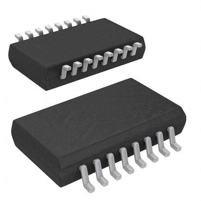
| 供应商器件封装 | 16-SOIC |
| 其它名称 | AD421BRZRLCT |
| 分辨率(位) | 16 b |
| 包装 | 剪切带 (CT) |
| 安装类型 | 表面贴装 |
| 封装/外壳 | 16-SOIC(0.295",7.50mm 宽) |
| 工作温度 | -40°C ~ 85°C |
| 数据接口 | MICROWIRE™,串行 |
| 标准包装 | 1 |
| 电压-电源 | 3V,3.3V,5V |
| 电压源 | 单电源 |
| 类型 | DAC |
| 采样率(每秒) | - |


- 商务部:美国ITC正式对集成电路等产品启动337调查
- 曝三星4nm工艺存在良率问题 高通将骁龙8 Gen1或转产台积电
- 太阳诱电将投资9.5亿元在常州建新厂生产MLCC 预计2023年完工
- 英特尔发布欧洲新工厂建设计划 深化IDM 2.0 战略
- 台积电先进制程称霸业界 有大客户加持明年业绩稳了
- 达到5530亿美元!SIA预计今年全球半导体销售额将创下新高
- 英特尔拟将自动驾驶子公司Mobileye上市 估值或超500亿美元
- 三星加码芯片和SET,合并消费电子和移动部门,撤换高东真等 CEO
- 三星电子宣布重大人事变动 还合并消费电子和移动部门
- 海关总署:前11个月进口集成电路产品价值2.52万亿元 增长14.8%


PDF Datasheet 数据手册内容提取
a Loop-Powered 4 mA to 20 mA DAC AD421 FEATURES FUNCTIONAL BLOCK DIAGRAM 4 mA to 20mA Current Output HART® Compatible REF IN REF OUT1 REF OUT2 16-Bit Resolution and Monotonicity (+2.5V) (+1.25V) (+2.5V) LV VCC (cid:2)0.01% Integral Nonlinearity 5V or 3V Regulator Output 112.5k(cid:1) 75k(cid:1) 2.5V and 1.25V Precision Reference 750(cid:3)A Quiescent Current max AD421 134k(cid:1) Programmable Alarm Current Capability BANDGAP DRIVE Flexible High Speed Serial Interface REFERENCE 16-Lead SOIC and PDIP Packages 121k(cid:1) COMP LOCAL BOOST OSCILLATOR DATA INPUT SHIFT CLOCK REGISTER SWITCHED 16-BIT CURRENT LATCH DAC LATCH SIGMA- SOURCES GENERAL DESCRIPTION DELTA DAC AND 40(cid:1) The AD421 is a complete, loop-powered, digital to 4 mA to POWER-ON FILTERING 80k(cid:1) LOOP 20mA converter, designed to meet the needs of smart trans- RESET RTN mitter manufacturers in the Industrial Control industry. It pro- vides a high precision, fully integrated, low cost solution in a COM C1 C2 C3 compact 16-lead package. The AD421 is ideal for extending the PRODUCT HIGHLIGHTS resolution of smart 4 mA to 20mA transmitters at very low cost. 1. The AD421 is a single chip, high performance, low cost The AD421 includes a selectable regulator that is used to power solution for generating 4 mA to 20mA signals for smart itself and other devices in the transmitter. This regulator pro- industrial control transmitters. vides either a +5V, +3.3V or +3V regulated output voltage. 2. The AD421’s regulated supply voltage can be used to power The part also contains +1.25V and +2.5V precision references. any additional circuits in the transmitter. The regulated The AD421 thus eliminates the need for a discrete regulator output value is pin selectable as either +3V, +3.3V or +5V. and voltage reference. The only external components required are a number of passive components and a pass transistor to 3. The AD421’s on-chip references can provide a precision span large loop voltages. reference voltage to other devices in the system. This refer- ence voltage can be either +1.25V or +2.5V. The AD421 can be used with standard HART FSK protocol communication circuitry without any degradation in specified 4. The AD421 is fully compatible with standard HART cir- performance. The high speed serial interface is capable of oper- cuitry or other similar FSK protocols. ating at 10Mbps and allows for simple connection to com- 5. With the addition of a single discrete transistor, the AD421 monly-used microprocessors and microcontrollers via a standard can be operated from V + 2 V min to a maximum of the three-wire serial interface. CC breakdown voltage of the pass transistor. The sigma-delta architecture of the DAC guarantees 16-bit 6. The AD421 converts the digital data to current with 16-bit monotonicity while the integral nonlinearity for the AD421 is resolution and monotonicity. Full-scale settling time to ±0.01%. The part provides a zero scale 4mA output current ±0.1% typically occurs within 8ms. with ±0.1% offset error and a 20mA full-scale output current with ±0.2% gain error. 7. The AD421 features a programmable alarm current capabil- ity that allows the transmitter to send out of range currents to The AD421 is available in a 16-lead, 0.3 inch-wide, plastic DIP indicate a transducer fault. and in a 16-lead, 0.3 inch-wide, SOIC package. The part is speci- fied over the industrial temperature range of –40°C to +85°C. HART is a registered trademark of the HART Communication Foundation. REV. C Information furnished by Analog Devices is believed to be accurate and reliable. However, no responsibility is assumed by Analog Devices for its use, nor for any infringements of patents or other rights of third parties One Technology Way, P.O. Box 9106, Norwood, MA 02062-9106, U.S.A. which may result from its use. No license is granted by implication or Tel: 781/329-4700 World Wide Web Site: http://www.analog.com otherwise under any patent or patent rights of Analog Devices. Fax: 781/326-8703 © Analog Devices, Inc., 2000
AD421–LOOP-POWERED SPECIFICATIONS(Using DN25D1 as pass transistor as per Figure 3; REF IN = REF OUT2; T = T to T unless otherwise noted) A MIN MAX Parameter B Versions2 Units Conditions/Comments OUTPUT CHARACTERISTICS Current Loop Voltage Compliance3 V + 2 V min CC 350 V max DN25D Breakdown Voltage Full-Scale Settling Time 8 ms typ Settling Time to ±0.1%, C1 = C2 = 10nF, C3 = 3.3 nF Output Impedance 25 MΩ typ AC Loop Voltage Sensitivity 2 µA/V typ 1200 Hz to 2200 Hz VOLTAGE REGULATOR Output Voltage (V ) CC 3V Mode 2.95/3.05 V min/V max 3V Nominal. LV Pin Connected to V CC 3.3V Mode 3.25/3.35 V min/V max 3.3V Nominal. LV Pin Connected Through 0.01µF to V CC 5V Mode 4.95/5.05 V min/V max 5V Nominal. LV Pin Connected to COM Externally Available Current 3.25 mA min Assuming 4mA Flowing in the Loop Line Regulation 1 µV/V typ Load Regulation 15 µV/mA typ DAC SPECIFICATIONS (V = +3V to +5V; REF IN = REF OUT2; T = T to T unless otherwise noted) CC A MIN MAX Parameter B Versions2 Units Conditions/Comments ACCURACY Resolution 16 Bits Monotonicity 16 Bits min Integral Nonlinearity ±0.01 % of FS max FS = Full-Scale Output Current Offset (4mA) @ +25°C4 ±0.1 % of FS max V = 5 V CC Offset Drift ±25 ppm of FS/°C max Includes On-Chip Reference Drift Total Output Error (20mA) @ +25°C4 ±0.2 % of FS max V = 5 V CC Total Output Drift ±50 ppm of FS/°C max Includes On-Chip Reference Drift V Supply Sensitivity 50 nA/mV max 25nA/mV Typical CC VOLTAGE REFERENCE REF OUT2 Output Voltage 2.49/2.51 V min/V max 2.5V Nominal Drift ±40 ppm/°C max 20 ppm/°C Typical from –40°C to +25°C and –2.5 ppm/°C Typical from +25°C to +85°C Externally Available Current 0.5 mA min V Supply Sensitivity 150 µV/V max 15µV/V Typical CC Output Impedance 3 Ω typ Noise (0.1Hz–10Hz) 6 µV (p-p) typ REF OUT1 Output Voltage 1.24/1.26 V min/V max 1.25V Nominal, 100kΩ Load to COM5 Drift ±50 ppm/°C max 20 ppm/°C Typical from –40°C to +25°C and 2 ppm/°C Typical from +25°C to +85°C Externally Available Current 0.5 mA min V Supply Sensitivity 150 µV/V max 15µV/V Typical CC Output Impedance 3 Ω typ Noise (0.1Hz–10Hz) 4 µV (p-p) typ REF IN Input Resistance 40 kΩ typ DIGITAL INPUTS V (Logic 1) 0.75 × V V min IH CC V (Logic 0) 0.25 × V V max IL CC I ±10 µA max V = V IH IN CC I ±10 µA max V = 0V IL IN Data Coding Binary Data Rate 10 Mbps max POWER SUPPLIES Operating Range +2.95 to +5.05 V min to Vmax Functional to 7 V Quiescent Current @ V = 3 V 650 µA max 475µA Typical CC @ V = 5 V 750 µA max 575µA Typical CC NOTES 1The DN25D is available from Supertex, Inc., 1350 Bordeaux Drive, Sunnyvale, CA 94089. 2Temperature range is –40°C to +85°C. 3The max current loop voltage compliance is determined by the pass transistor breakdown voltage and is 350V for the DN25D. 4With V = 3 V, the transfer function shifts negative by typically 0.25%; a 16 kΩ resistor connected between COM and LOOPRTN will approximately compensate for the V CC CC supply sensitivity in moving from 5 V to 3 V by skewing the gain of the AD421. 5100kΩ resistor only required if this reference is being used in application circuits. Specifications subject to change without notice. –2– REV. C
AD421 TIMING CHARACTERISTICS1, 2, 3 (V = +3V to +5V, T = T to T unless otherwise noted) CC A MIN MAX Parameter (B Versions) Units Conditions/Comments t 100 ns min Data Clock Period CK t 50 ns min Data Clock Low Time CL t 50 ns min Data Clock High Time CH t 30 ns min Data Stable Width DW t 30 ns min Data Setup Time DS t 0 ns min Data Hold Time DH t 50 ns min Latch Delay Time LD t 50 ns min Latch Low Time LL t 50 ns min Latch High Time LH NOTES 1Guaranteed by characterization at initial product release, not production tested. 2See Figures 1 and 2. 3All input signals are specified with tr = tf = 5 ns (10% to 90% of V ) and timed from a voltage level of (V + V )/2; tr and tf should not exceed 1µs on any digital CC IN IL input. Specifications subject to change without notice. CLOCK WORD "N" WORD "N +1" DATA 1 0 1 1 0 0 1 0 0 1 1 1 0 0 1 1 1 0 0 1 MSB)B15 B14 B13B12 B11 B10 B9 B8 B7 B6 B5 B4 B3 B2 B1B0LSB) B15 B14 B13 B12 ( ( LATCH Figure 1.Serial Interface Waveforms (Normal Data Load) t CK t CL CLOCK t CH t t DS DH DATA t DW t LD t LL LATCH t LH Figure 2.Serial Interface Timing Diagram REV. C –3–
AD421 ABSOLUTE MAXIMUM RATINGS* PIN CONFIGURATION (T = +25°C unless otherwise noted) A DIP and SOIC DRIVE, BOOST, COMP to COM . . . –0.5 V to V + 0.5 V CC LOOP RTN to COM . . . . . . . . . . . . . . . . . . . –2 V to + 0.5 V Digital Input Voltage to COM . . . . . . . –0.5 V to V + 0.5 V CC REF OUT1 1 16 VCC Operating Temperature Range REF OUT2 2 15 BOOST Commercial (B Version) . . . . . . . . . . . . . . –40°C to +85°C Storage Temperature Range . . . . . . . . . . . . –65°C to +150°C REF IN 3 14 COMP Junction Temperature . . . . . . . . . . . . . . . . . . . . . . . . +150°C LV 4 AD421 13 DRIVE Plastic DIP Package, Power Dissipation . . . . . . . . . . 670 mW LATCH 5 TOP VIEW 12 C1 (NOT TO SCALE) θ Thermal Impedance . . . . . . . . . . . . . . . . . . . . 116°C/W CLOCK 6 11 C2 JA Lead Temperature (Soldering, 10 sec) . . . . . . . . . . . . 260°C DATA 7 10 C3 SOIC Package, Power Dissipation . . . . . . . . . . . . . . . 450 mW LOOP RTN 8 9 COM θ Thermal Impedance . . . . . . . . . . . . . . . . . . . . 110°C/W JA Lead Temperature, Soldering Vapor Phase (60 sec) . . . . . . . . . . . . . . . . . . . . . +215°C Infrared (15 sec) . . . . . . . . . . . . . . . . . . . . . . . . . +220°C ORDERING GUIDE *Stresses above those listed under Absolute Maximum Ratings may cause perma- Temperature Package nent damage to the device. This is a stress rating only; functional operation of the Model Range Option* device at these or any other conditions above those listed in the operational sections of this specification is not implied. Exposure to absolute maximum rating AD421BN –40°C to +85°C N-16 conditions for extended periods may affect device reliability. AD421BR –40°C to +85°C R-16 AD421BRRL –40°C to +85°C R-16; Reeled SOIC EVAL-AD421EB Evaluation Board *N = Plastic DIP, R = SOIC. CAUTION ESD (electrostatic discharge) sensitive device. Electrostatic charges as high as 4000V readily WARNING! accumulate on the human body and test equipment and can discharge without detection. Although these devices feature proprietary ESD protection circuitry, permanent damage may occur on devices subjected to high energy electrostatic discharges. Therefore, proper ESD precautions are recommended to avoid performance degradation or loss of functionality. ESD SENSITIVE DEVICE –4– REV. C
AD421 PIN FUNCTION DESCRIPTIONS Pin No. Mnemonic Function 1 REF OUT1 Reference Output 1. A precision +1.25V reference is provided at this pin. It is intended as a precision ref- erence source for other devices in the transmitter. REF OUT1 is a buffered output capable of providing up to 0.5mA to external circuitry. If REF OUT 1 is required to sink current, a resistive load of 100 kΩ to COM should be added. (See Reference section.) 2 REF OUT2 Reference Output 2. A precision +2.5V reference is provided at this pin. To operate the AD421 with its own reference, REF OUT2 should be connected to REF IN. It can also be used as a precision reference source for other devices in the transmitter. REF OUT2 is a buffered output capable of providing up to 0.5mA to external circuitry. 3 REF IN Voltage Reference Input. The reference voltage for the AD421 is applied to this pin and it sets the span for the AD421. The nominal reference voltage for the AD421 is +2.5V for correct operation. This can be sup- plied using an external reference source or by using the part’s own REF OUT2 voltage. 4 LV Regulated Voltage Control Input. The LV input controls the loop gain of the servo amplifier to set V . CC With LV connected to COM, the regulator voltage is set to 5V nominal. If the LV input is connected through 0.01µF to V , the regulated voltage is nominally 3.3V. With LV connected to V the regulated voltage, CC CC V , is 3V nominal. CC 5 LATCH DAC Latch Input. Logic Input. A rising edge of the LATCH signal loads the data from the serial input shift register to the DAC latch and hence updates the output of the DAC. The number of clock cycles provided between latch pulses determines whether the DAC is in alarm or normal current mode. (See Digital Inter- face section.) 6 CLOCK Data Clock Input. Data on the DATA input is clocked into the shift register on the rising edge of this CLOCK input. The period of this clock equals the input serial data bit rate. This serial clock rate can be up to 10MHz. If 16 clock cycles are provided between LATCH pulses then the data on the DATA input is accepted as normal 4–20mA data. If more than 16 clock cycles are provided between LATCH pulses, the data is assumed to be alarm current data (see Digital Interface section). 7 DATA Data Input. The data to be loaded to the AD421 input shift register is applied to this input. Data should be valid on the rising edge of the CLOCK input. 8 LOOP RTN Loop Return Output. LOOP RTN is the return path for current flowing in the current loop. 9 COM Common. This is the reference potential for the AD421 analog and digital inputs and outputs and for the voltage regulator output. 10 C3 Filtering Capacitor. A low dielectric absorption capacitor ceramic capacitor should be connected between this pin and COM for internal filtering of the switched current sources. 11 C2 Filtering Capacitor. See C3 description. 12 C1 Filtering Capacitor. See C3 description. 13 DRIVE Output from the Voltage Regulator Loop. The DRIVE signal controls the external pass transistor to establish and maintain the correct V level programmed by the LV inputs while providing the necessary bias as the loop cur- CC rent is programmed from 4mA to 20mA. 14 COMP Compensation Capacitor Input. A capacitor connected between COMP and DRIVE is required to stabilize the feedback loop formed with the regulator op amp and the external pass transistor. 15 BOOST This open collector pin sinks the necessary current from the loop so that the current flowing into BOOST plus the current flowing into COM is equal to the programmed loop current. 16 V Power Supply. V is the power supply input of the AD421 and it also provides the voltage regulator output, CC CC driven by the external pass transistor. It is used both to bias the AD421 itself and to provide power for the rest of the smart transmitter circuitry. The LV input determines the regulated voltage output to be either 3V, 3.3V or 5V nominal. Alternatively, a separate power supply can be connected to this pin to power the AD421. V should be decoupled to COM with a 2.2 µF capacitor. CC REV. C –5–
AD421 CIRCUIT DESCRIPTION Table I. FET Characteristics The AD421 is designed for use in loop-powered 4–20mA smart transmitter applications. A smart transmitter, as a remote in- FET Type N-Channel Depletion Mode strument, controls its current output signal on the same pair of I 24mA min DSS wires from which it receives its power. The AD421 essentially provides three primary functions in the smart transmitter. These BVDS (VLOOP – VCC) min functions are a DAC function for converting the microprocessor/ V V max PINCHOFF CC microcontroller’s digital data to analog format, a current amp- lifier which sets the current flowing in the loop and a voltage Power Dissipation 24 mA × (VLOOP – VCC) min regulator to provide a stable operating voltage from the loop where V is the operating voltage of the AD421 and V is supply. The part also contains a high speed serial interface, two CC LOOP the loop voltage. buffered output references and a clock oscillator circuit. The different sections of the AD421 are discussed in more detail The DN25D FET transistor from Supertex1 meets all the above below. requirements for the FET. Other suitable transistors include ND2020L and ND2410L, both from Siliconix. Voltage Regulator The voltage regulator consists of an op amp, bandgap reference There are a number of external components required to com- and an external depletion mode FET pass transistor. This cir- pensate the regulator loop and ensure stable operation. The cuit is required to regulate the loop voltage that powers the capacitor from the V pin to the COM pin is required to CC AD421 itself and the rest of the transmitter circuitry. Figure 3 stabilize the regulator loop. shows the voltage regulator section of the AD421 plus the associ- To provide additional compensation for the regulator loop, a ated external circuitry for a VCC of 3.3 V. compensation capacitor of 0.01µF should be connected between the COMP and DRIVE pins and an external circuit LOOP(+) of a 1kΩ resistor and a 1000pF capacitor in series should be VCC TO EXTERNAL DN25D connected between DRIVE and COM to stabilize this feed- CIRCUITRY back loop formed with the regulator op amp and the external 2.2(cid:3)F 0.01(cid:3)F pass transistor. COM LV VCC DAC Section AD421 112.5k(cid:1) 75k(cid:1) The AD421 contains a 16-bit sigma-delta DAC to convert the digital information loaded to the input latch into a current. The 134k(cid:1) sigma-delta architecture is particularly useful for the relatively DRIVE 1.21V low bandwidth requirements of the industrial control environ- RBEAFNERDEGNACPE COMP 0.01(cid:3)F ment because of its inherent monotonicity at high resolution. 121k(cid:1) 1k(cid:1) The AD421 guarantees monotonicity to the 16-bit level. 1000pF The sigma-delta DAC consists of a second order modulator followed by a continuous time filter. The single bit stream from Figure 3.AD421 Voltage Regulator Circuit to Provide the modulator controls a switched current source. This current V = 3.3 V CC source is then filtered by three resistor-capacitor filter sections. The signal on the LV pin selects the voltage to which VCC The resistors for each of the filter sections are on-chip while regulates by changing the gain of the resistor divider between the capacitors are external on the C1–C3 pins. To meet the the op amp inverting input and the VCC pin. As the LV pin specified full-scale settling on the part, low dielectric absorption varies between COM and VCC, the voltage from the regulator capacitors (NPO) are required. Suitable values for these capacitors loop varies between 3V and 5V nominal. With LV connected are C1 = 0.01µF, C2 = 0.01µF, and C3 = 0.0033µF. to COM, the regulated voltage is 5V; with LV connected Current Amplifier through a 0.01µF capacitor to V , the regulated voltage is CC The DAC output current drives the second section, an opera- 3.3V while if LV is connected to V , the regulated voltage CC tional amplifier and NPN transistor which acts as a current is 3V. amplifier to set the current flowing through the LOOP RTN The range of loop voltages that can be used by the configuration pin. Figure 4 shows the current amplifier section of the AD421. shown in Figure 3 is determined by the FET breakdown and An 80kΩ resistor connected between the DAC output and loop saturation voltages. The external FET parameters such as Vgs return is used as a sampling resistor to determine current. The (off), IDSS and transconductance must be chosen so that the op base drive to the NPN transistor servos the voltage across the amp output on the DRIVE pin can control the FET operating 40Ω resistor to equal the voltage across the 80kΩ resistor. point while swinging in the range from V to COM. CC The main characteristics for selecting the FET pass transistor are as follows: –6– REV. C
AD421 Reference Section SWITCHED AD421 The AD421 contains an on-chip 1.21V bandgap reference CURRENT which is used as part of the voltage regulator loop. A bandgap SOURCES reference is also used to generate two references voltages BOOST which are available for use external to the AD421. Figure 5 shows the reference section of the AD421. The REF OUT1 pin 80k(cid:1) provides a buffered +1.25V reference voltage which can supply 40(cid:1) up to 0.5mA of external current. The REF OUT2 pin provides LOOP RTN a +2.5V reference voltage which is also capable of providing Figure 4.Current Amplifier 0.5mA of external current. To use the AD421 with its own reference, simply connect the REF OUT2 pin to the REF IN The BOOST pin is normally tied to the V pin. As the DAC CC pin of the device. Alternatively, the part can be used with an input code varies from all zeros to full scale, the output current external reference by connecting the external reference between from the NPN transistor and thus the total loop current varies REF IN and COM. from 4mA to 20mA. With BOOST and V tied together, the CC external FET (DN25D) has to supply the full range of loop When REFOUT1 and REFOUT2 are used in application current (4mA to 20mA). circuits, external 4.7µF capacitors are required on the reference pins to provide compensation and ensure stable operation of the Digital Interface references. These capacitors can be omitted if the internal refer- The digital interface on the AD421 consists of just three wires: ences are not required. DATA, CLOCK and LATCH. The interface connects directly to the serial ports of commonly-used microcontrollers without the need for any external glue logic. Data is loaded MSB first 4.7(cid:3)F 4.7(cid:3)F into an input shift register on the rising edge of the CLOCK REF OUT1 REF OUT2 signal and is transferred to the DAC latch on the rising edge of (1.25V) (2.5V) LV VCC the LATCH signal. The timing diagrams for the serial interface are shown in Figure 1 and Figure 2. AD421 112.5k(cid:1) 75k(cid:1) The data to be loaded to the AD421’s input shift register takes 50k(cid:1) 134k(cid:1) two forms; normal 4mA to 20mA data or alarm current data. 2.5V 1.21V DRIVE The first form is where the AD421 operates over its normal 50k(cid:1) BANDGAP REFERENCE 4mA to 20mA output range with 16 bits of resolution between 121k(cid:1) these endpoints. The second form allows the user to program a current value outside this range as an indication from the trans- mitter than there is a problem with the transducer. The AD421 Figure 5.Reference Section counts the number of clock pulses which it receives between REF OUT2 is sensed internally, and if more than 0.5mA is LATCH signals as a means of determining whether the data drawn externally from this reference, the chip goes into a power clocked in is 4mA to 20mA data or alarm current data. on reset state. In this state the sigma-delta DAC is disabled, the If there are 16 rising clock edges between successive LATCH internal oscillator is stopped and the input data latch is cleared. pulses, then the data being loaded to the input shift register is REF OUT1 has limited current sinking capability. If REF assumed to be normal 4mA to 20mA data. On the rising edge OUT1 is required to sink current, a resistive load of 100kΩ of the LATCH signal, the input shift register data is transferred to COM should be added in addition to the 4.7µF capacitor. to the DAC latch in a 16-bit parallel transfer. In this case, the 16 bits of data in the DAC latch program the output current USING THE AD421 between 4mA for all 0s and 20mA for all 1s (see Table II). The AD421 can be programmed for normal 4 mA to 20mA Data transferred to the AD421 should be MSB first. operation or for alarm current operation. For normal operation, If there are more than 16 clock pulses between successive the coding is 16-bit straight (natural) binary over an output LATCH pulses, then the data being loaded to the input shift current range of 4mA to 20mA. For alarm current operation, register is assumed to be alarm current data. In this case, the the coding is also straight binary but with 17bits of resolution AD421 accepts 17 bits of data into its shift register. For situa- over twice the span, 0mA to 32mA, although the part should tions where there are more than 17 clocks in the serial write not be programmed outside the range of 3.5mA to 24mA. To operation (for example, 24 clocks in a 3 × 8-bit transfer from the determine whether data written to the part is normal 4 mA to serial port of a microcontroller) the AD421 simply accepts the 20mA data or alarm current data, the number of clock pulses last 17 bits of the serial write operation. Data transferred in this between two successive LATCH pulses are counted. If the num- serial write operation is LSB last (i.e., the MSB is loaded on the ber of pulses is 0–16 (modulo 32), it chooses normal mode; if it 17th rising clock edge prior to the LATCH pulse). On the rising is 17–31 (modulo 32), it chooses alarm current range. edge of the LATCH signal, the input shift register data is trans- 4 mA to 20mA Coding ferred to the DAC latch in a 17-bit parallel transfer. In this Table II shows the ideal input-code-to-output-current relation- case, the 17 bits of data in the DAC latch program the output ship for normal operation of the AD421. The output current current between 0 mA for all 0s and 32mA for all 1s (see Table values shown assume a REFIN voltage of +2.5V. With a III). However, in practice the AD421 cannot reliably produce a REFIN of +2.5V, 1LSB = 16mA/65,536 = 244nA. Figure 6 current less than 3.5mA or more than 24mA. shows a timing diagram for programming the AD421 for normal 4 mA to 20mA operation, the AD421 outputting a current REV. C –7–
AD421 of 11.147mA. With 16 clock pulses between consecutive latch CLOCK signals data written is for normal 4 mA to 20mA operation. WORD "N" Table II. Ideal Input/Output Code Table DATA XX XX XX X 0 00 1 11 1 0 0 0 0 0 00 0 00 for 4 mA to 20mA Operation Code Output Current XXXXXXXB)B16 B15B14B13B12B11B10B9B8 B7B6B5B4B3B2B1SB)B0 S L M ( 0000 0000 0000 0000 4mA ( 0000 0000 0000 0001 4.000244mA LATCH 0000 0000 0000 0010 4.000488mA Figure 7.Write Cycle for Programming Alarm Current 0100 0000 0000 0000 8mA Data 1000 0000 0000 0000 12mA MICROPROCESSOR INTERFACING 1100 0000 0000 0000 16mA AD421 – MC68HC11 (SPI BUS) INTERFACE 1111 1111 1111 1101 19.999268mA Figure 8 shows a typical interface between the AD421 and the 1111 1111 1111 1110 19.999512mA Motorola MC68HC11 SPI (Serial Peripheral Interface) bus. 1111 1111 1111 1111 19.999756mA The SCK, MOSI and SS pins of the 68HC11 are respectively connected to the CLOCK, DATA IN and LATCH pins of the AD421. CLOCK WORD "N" WORD "N +1" SCK CLOCK 68HC11 AD421* DATA 1 0 1 1 0 0 1 0 0 1 1 1 0 0 1 1 1 0 0 1 MOSI DATA IN MSB)B15 B14 B13B12 B11B10 B9B8B7 B6B5B4 B3 B2 B1B0LSB) B15 B14 B13B12 SS LATCH ( ( LATCH * ADDITIONAL PINS OMITTED FOR CLARITY Figure 8.AD421 to 68HC11 Interface A typical routine such as the one shown below begins by initializ- Figure 6.Write Cycle for 4 mA to 20mA Operation ing the state of the various SPI data and control registers. Alarm Current Coding INIT LDAA #$2F ;SS = 1; SCK = 0; MOSI = 1 Table III shows the ideal input-code-to-output-current relation- STAA PORTD ;SEND TO SPI OUTPUTS ship for alarm current programming of the AD421. In this case, LDAA #$38 ;SS, SCK, MOSI = OUTPUTS the equivalent span is 0mA to 32mA but a reliable operating STAA DDRD ;SEND DATA DIRECTION INFO span is 3.5mA to 24mA. The part may give an indeterminate LDAA #$50 ;DABL INTRPTS, SPI IS MASTER & ON output for code values outside the range given in the table. As a STAA SPCR ;CPOL = 0, CPHA = 0, 1MHZ BAUDRATE result, the user is advised to restrict the code programmed to the NEXTPT LDAA MSBY ;LOAD ACCUM W/UPPER 8 BITS part in alarm current mode to within the range shown in Table BSR SENDAT ;JUMP TO DAC OUTPUT ROUTINE III. Figure 7 shows a timing diagram for loading an alarm cur- JMP NEXTPT ;INFINITE LOOP rent of 3.75mA to the AD421 with an 8-bit microcontroller SENDAT LDY #$1000 ;POINT AT ON-CHIP REGISTERS using three 8-bit writes. BCLR $08,Y,$20;DRIVE SS (LATCH) LOW STAA SPDR ;SEND MS-BYTE TO SPI DATA REG The output current values shown assume a REFIN voltage of WAIT1 LDAA SPSR ;CHECK STATUS OF SPIE +2.5V. With a REFIN of +2.5V, an ideal 1LSB = 32mA/ BPL WAIT1 ;POLL FOR END OF X-MISSION 131,072 = 244nA. LDAA LSBY ;GET LOW 8 BITS FROM MEMORY STAA SPDR ;SEND LS-BYTE TO SPI DATA REG Table III. Ideal Input/Output Code Table WAIT2 LDAA SPSR ;CHECK STATUS OF SPIE BPL WAIT2; ;POLL FOR END OF X-MISSION for Alarm Current Operation BSET $08,Y,$20;DRIVE SS HIGH TO LATCH DATA Code Output Current RTS The SPI data port is configured to process data in 8-bit bytes. 0 0011 1000 0000 0000 3.5mA The most significant data byte (MSBY) is retrieved from 0 0011 1100 0000 0000 3.75mA memory and processed by the SENDAT routine. The SS pin is 0 0100 0000 0000 0000 4mA driven low by indexing into the PORTD data register and clear Bit 5. The MSBY is then sent to the SPI data register where it is 0 1000 0000 0000 0000 8mA automatically transferred to the AD421 internal shift resistor. 1 0000 0000 0000 0000 16mA 1 0100 0000 0000 0000 20mA 1 0110 0000 0000 0000 22mA 1 1000 0000 0000 0000 24mA –8– REV. C
AD421 The HC11 generates the requisite eight clock pulses with data VCC valid on the rising edges. After the MSBY is transmitted, the least significant byte (LSBY) is loaded from memory and 2.2(cid:3)F 0.1(cid:3)F transmitted in a similar fashion. To complete the transfer, the VCC LATCH pin is driven high when loading the complete 16-bit word into the AD421. 10k(cid:1) VCC CLOCK CLOCK AD421 TO MICROWIRE INTERFACE VCC The flexible serial interface of the AD421 is also compatible AD421* with the National Semiconductor MICROWIRE interface. The 10k(cid:1) MICROWIRE interface is used in microcontrollers such as the LATCH LATCH COP400 and COP800 series of processors. A generic interface VCC to use the MICROWIRE interface is shown in Figure 9. The G1, SK, and SO pins of the MICROWIRE interface respec- 10k(cid:1) tively connect to the LATCH, CLOCK, and DATA IN pins of DATA IN DATA IN the AD421. COM SK CLOCK * ADDITIONAL PINS OMITTED FOR CLARITY MICROWIRE AD421* Figure 10.Opto-Isolated Interface SO DATA IN APPLICATIONS SECTION G1 LATCH Basic Operating Configuration Figure 11 shows the basic connection diagram for the AD421 * ADDITIONAL PINS OMITTED FOR CLARITY operating at 5 V. This circuit shows the minimum of external Figure 9.AD421 to MICROWIRE Interface components to operate the AD421. In the diagram, the AD421’s Opto-Isolated Interface regulator loop in conjunction with the DN25D pass transistor The AD421 has a versatile serial 3-wire serial interface making provides the V voltage for the AD421 itself and for other CC it ideal for minimizing the number of control lines required for devices in the transmitter. The V pin should be well decou- CC isolation of the digital system from the control loop. In intrinsi- pled with a 2.2 µF capacitor to ensure regulator stability and to cally safe applications or due to noise, safety requirements, or absorb power glitches on the V line of the AD421 and other CC distance, it may be necessary to isolate the AD421 from the devices in the system. If the AD421 is operated with V = 3 V, CC controller. This can easily be achieved by using opto-isolators. the transfer function shifts negative. To correct for this a 16kΩ Figure 10 shows an opto-isolated interface to the AD421 where resistor connected between COM and LOOPRTN will approxi- CLOCK, DATAIN and LATCH are driven from opto-couplers. mately compensate for the V supply sensitivity in moving from CC Be aware of signal inversion across the opto-couplers. If opto- 5V to 3V by adjusting the gain of the AD421. couplers with relatively slow rise and fall times are used, Schmitt triggers may be required on the digital inputs to prevent errone- ous data being presented to the DAC. VCC TO EXTERNAL DN25D CIRCUITRY 4.7(cid:3)F 2.2(cid:3)F COM REF IN REF OUT2 REF OUT1 COM LV VCC DRIVE DATA COMP 0.01(cid:3)F VLOOP CLOCK 1k(cid:1) AD421 1000pF LATCH BOOST LOOP RTN COM C1 C2 C3 COM TO EXTERNAL 0.01(cid:3)F 0.01(cid:3)F 0.0033(cid:3)F CIRCUITRY Figure 11. Basic Connection Diagram REV. C –9–
AD421 A capacitor of 0.01µF connected between COMP and DRIVE Smart Transmitter is required to stabilize the feedback loop formed with the The AD421 is intended for use in 4 mA to 20mA smart trans- regulator op amp and the external pass transistor. An external mitters. A smart transmitter is a system that incorporates a snubber circuit of 1kΩ and 1000pF is required between the microprocessor system which is used for linearization and DRIVE pin and COM and a 0.1µF cap between COMP and communication. Figure 13 shows a block diagram of a typical DRIVE to stabilize the feedback loop formed by the regulator smart transmitter. In this example, the transmitter does not have op amp and the external pass transistor. any digital communication capabilities. The internal 2.5V reference on the AD421 is used as the refer- ence for the AD421 and this has to be decoupled with a 4.7µF MEMORY capacitor for compensation and stability purposes. The sigma- delta DAC on the part consists of a second order modulator followed by a continuous time filter. The resistors for each of 4mA TO 20mA A/D MICRO- D/A the filter sections are on-chip while the capacitors are external SENSORS CONVERTER PROCESSOR CONVERTER MEASUREMENT on the C1 to C3 pins. To meet the specified full-scale settling CIRCUIT on the part, low dielectric absorption capacitors (NPO) are Figure 13.Typical Smart Transmitter required. Suitable values for these capacitors are C1 = C2 = Figure 14 shows a typical smart transmitter application circuit 0.01 µF, and C3 = 0.0033 µF. using the AD421. The digital interface on the AD421 consists of just three wires: The sensor voltage to be measured at the transmitter is con- DATA, CLOCK and LATCH. The interface connects directly verted using a high resolution sigma-delta converter such as to the serial ports of commonly-used microcontrollers without the AD7714 or AD7715. These devices have an on-board PGA the need for any external glue logic. Data is loaded into an input which can provide gains on the analog front end from 1 to 128. shift register on the rising edge of the CLOCK signal and is This allows for an analog input range as low as 10mV which transferred to the DAC latch on the rising edge of the LATCH allows the transducer to be connected directly to the ADC. The signal. AD7714/AD7715 have digital calibration techniques which are Reduce Power Load on External FET used to eliminate gain and offset errors. In addition, back- Figure 12 shows a circuit where an external NPN transistor is ground calibration techniques are provided whereby the part added to reduce the power loading on the FET. The FET will continually calibrates itself and the user does not have to supply the VCC and an external high voltage NPN bipolar tran- worry about issuing periodic calibration commands to remove sistor can carry the BOOST current. The BOOST pin sinks the effects of time and temperature drift. necessary current from the loop so that the current flowing into In normal operation the microprocessor reads the data from the BOOST plus the current flowing into COM is equal to the AD7714/AD7715. After the data is processed by the micro- programmed loop current. The external NPN transistor reduces controller, the data is transferred from the serial port of the the external power load that the FET has to carry to less than processor to the AD421 for transmission over the 4 to 20mA 750µA if no other components share the V line and to less CC loop back to the control center. than 4mA in applications that share the same V line as the CC AD421. The AD421 regulates the loop voltage to create power for the rest of the transmitter circuitry. In Figure 14, the derived V CC voltage is 3.3V which is achieved by connecting the LV pin to LOOP(+) V through 0.01µF. REF OUT2 provides the reference volt- VCC TO EXTERNAL DN25D CC CIRCUITRY age for the AD421 itself while REF OUT1 provides the refer- BC639/BC337 2.2(cid:3)F ence voltage for the AD7714/AD7715. COM LV VCC 112.5k(cid:1) 75k(cid:1) AD421 134k(cid:1) DRIVE RBEAFNERDEGNACPE 1.21V COMP0.01(cid:3)F 1k(cid:1) 121k(cid:1) 1000pF BOOST 80k(cid:1) 40(cid:1) LOOP RTN LOOP(–) Figure 12.External NPN Transistor Reduces Power Load on FET –10– REV. C
AD421 DN25D 3.3V 0.1(cid:3)F 2.2(cid:3)F 0.01(cid:3)F SENSORS DVDD AVDD BOOST VCC LV mV (cid:1)R TTDC REF IN 1.25V REF OUT1 ANATOLOG 100k(cid:1) 4.7(cid:3)F VCC 4.7(cid:3)F RREEFF IONUT2 0.01(cid:3)F PLOOWOEPR AMBIENT DIGITAL COMP TEMP CONVERTER SENSOR CLOCK DRIVE AD7714/ AD7715 MICROCONTROLLER LATCH 1k(cid:1) DATA 1000pF MCLK IN AD421 GND MCLK OUT CS LOOP DATA OUT RTN COM SCLK DATA IN C1 C2 C3 DGND AGND Figure 14.AD421 in Smart Transmitter Application HART Interfacing Figure 16 shows a block diagram of a smart and intelligent The HART protocol uses a frequency shift (FSK) keying tech- transmitter. An intelligent transmitter is a transmitter in which nique based on the Bell 202 Communication Standard which is the functions of the microprocessor are shared between deriving one of several standards used to transmit digital signals over the primary measurement signal, storing information regarding the telephone lines. This technique is used to superimpose the transmitter itself, its application data and its location and digital communication on to the 4 mA to 20mA current loop also managing a communication system which enables two way connecting the central system to the transmitter in the field. communication to be superimposed on the same circuit that Two different frequencies, 1200Hz and 2200Hz, are used to carries the measurement signal. A smart transmitter incorporat- represent binary 1 and 0 respectively, as shown in Figure 15. ing the HART protocol is an example of a smart intelligent These sine wave tones are superimposed on the dc signal at a transmitter. low level with the average value of the sine wave signal being zero. This allows simultaneous analog and digital communica- tions. Additionally, no dc component is added to the existing MEMORY 4 mA to 20mA signal regardless of the digital data being sent over the line. Consequently, existing analog instruments con- tinue to work in systems that implement HART as the low-pass A/D MICRO- D/A 4mA TO 20mA SENSORS filtering usually present effectively removes the digital signal. A CONVERTER PROCESSOR CONVERTER MEASUREMENT CIRCUIT single pole 10Hz low-pass filter effectively reduces the commu- nication signal to a ripple of about ±0.01% of the full-scale COMMUNICATION SYSTEM signal. The HART protocol specifies that master devices like a host control system or a hand held terminal transmit a voltage Figure 16.Smart and Intelligent Transmitter signal whereas a slave or field device transmits a current signal. Figure 17 shows an example of the AD421 in a HART transmit- The current signal is converted into a corresponding voltage by ter application. Most of the circuit is as outlined in the smart the loop load resistor. transmitter as shown in Figure 14. The HART data transmitted on the loop is received by the transmitter using a bandpass filter APPROX and modem and the HART data is transferred to the micro- +0.5mA controller’s UART or asynchronous serial port. HART data to be transmitted on the loop is sent from the microcontroller’s UART or asynchronous serial port to the modem. It is then waveshaped before being coupled onto the AD421’s output at the C3 pin. The value of the coupling capacitor C is determined C by the waveshaper output and the C3 capacitor of the AD421. The blocks containing the Bell 202 Modem, waveshaper and bandpass filter come in a complete solution with the 20C15 from Symbios APPROX –0.5mA 1200Hz 2200Hz Logic, Inc., or HT2012 from SMAR Research Corp. “1” “0” For a more complete AD421-20C15 interface, please refer to Figure 15.HART Transmission of Digital Signals Application Note AN-534 on the Analog Devices’ website www.analog.com or contact your local sales office. REV. C –11–
AD421 DN25D 3.3V 0.01(cid:3)F 0.1(cid:3)F 2.2(cid:3)F SENSORS DVDD AVDD BOOST VCC LV 1.25V mV (cid:1)R TTDC ANALROEGF IN 100k(cid:1) 4.7(cid:3)F 4.7(cid:3)F RREEFF OOUUTT12 0.01(cid:3)F PLOOWOEPR AMBIENT DIGTIOTAL VCC REF IN COMP TEMP CONVERTER SENSOR AD7714/ CLOCK DRIVE MICROCONTROLLER AD7715 LATCH 1k(cid:1) DATA MCLK IN AD421 1000pF GND MCLK OUT CS LOOP DATA OUT RTN COM SCLK DATA IN C1 C2 C3 DGND AGND CC* WAVEFORM BANDPASS HART SHAPER FILTER MODEM BELL 202 HT20C12/20C15 *FOR SELECTION OF CC, REFER TO AN-534 Figure 17.AD421 in HART Transmitter Application Current Source across R2. The ratio of R1 to R2 determines the current that Figure 18 shows an application circuit for the AD421 being flows in the load resistor R . I = [1 + R1/R2] × I , where I L L PROG L used as a current source. The current programmed to the is the current that flows in the load resistor R and I is the L PROG AD421 (4 mA to 20mA) will develop a voltage across R1. current programmed to the AD421. R1 and R2 are external to This same voltage due to negative feedback will be generated the AD421 and will need to be matched resistors to obtain a highly accurate current source. 5 VOLT +5V REGULATOR OUT IN VS 2.2(cid:3)F 10k(cid:1) 10k(cid:1) 4.7(cid:3)F COM COM COM 10k(cid:1) REF IN REF OUT2 REF OUT1 LV VCC DATA DATA DRIVE COMP CLOCK CLOCK AD421 BOOST LOOP RTN LATCH LATCH COM C1 C2 C3 R1 R2 0.01(cid:3)F 0.01(cid:3)F 0.0033(cid:3)F RL VS RETURN Figure 18.AD421 in Programmable Current Source/Sink –12– REV. C
AD421 Battery Backup Figure 19 shows an application circuit for the AD421 where the DN25D micro and memory sections of the circuitry are protected against IN3611 losing data if the loop is broken. The backup circuit switches 0.1(cid:3)F IRFF9113 4.7(cid:3)F from V to battery voltage without a glitch when V power is IN3611 lost. ThCeC IRFF9113 acts as a current source durinCgC normal VCC VLOOP 100k(cid:1) 2.2(cid:3)F operation and provides a constant charging current to the supercap MICRO/ MEMORY or Nicad. The loss of V drops the IRFF9113’s gate voltage to zero volts, which allowsC tChe battery or supercaps current to flow GND SUPERCAP VCC DRIVE through the MOSFETs channel and integral body diode to AD421* provide power for the micro and memory sections. To calibrate LOOP RTN this circuit, connect an ammeter in series with the battery or COM supercap. Then with V and the load present adjust the 100kΩ CC *ADDITIONAL CIRCUITRY OMITTED FOR CLARITY potentiometer for the battery charging current recommended by Figure 19.Battery Backup Circuit the battery or supercap manufacturer. Nonrechargeable batteries should not be used in this application due to danger of explosion. REV. C –13–
AD421 OUTLINE DIMENSIONS Dimensions shown in inches and (mm). 16-Lead Plastic DIP (N-16) 0.840 (21.34) 0.745 (18.92) v. C) 161 89 00..228400 ((76..1110)) 0.325 (8.26) 00 (re 0.300 (7.62) 0.195 (4.95) –3/ PIN 1 0.060 (1.52) 0.115 (2.93) 0 – 0.015 (0.38) b 0.210 (5.33) 5 MAX 0.130 10 0.160 (4.06) (3.30) C2 0.115 (2.93) MIN 0.015 (0.381) 0.022 (0.558) 0.100 0.070 (1.77) SEATING 0.008 (0.204) 0.014 (0.356) (2.54) 0.045 (1.15) PLANE BSC 16-Lead (Wide Body) Small Outline Package (R-16) 0.4133 (10.50) 0.3977 (10.00) 16 9 1 8 0.2992 (7.60)0.2914 (7.40)0.4193 (10.65)0.3937 (10.00) 0.0118 (0.30) PIN 1 00..10094236 ((22..6355)) 00..00209918 ((00..7245))x 45(cid:4) 0.0040 (0.10) 8(cid:4) 0.0500 (1.27) 0(B.10.S52C070) 00..00119328 ((00..4395)) SPELAANTIENG 00..00102951 ((00..3223))0(cid:4) 0.0157 (0.40) A. S. U. N D I E T N RI P –14– REV. C