ICGOO在线商城 > 集成电路(IC) > PMIC - LED 驱动器 > CS1616-FSZ

 Datasheet下载
- 型号: CS1616-FSZ
- 制造商: Cirrus Logic
- 库位|库存: xxxx|xxxx
- 要求:
| 数量阶梯 | 香港交货 | 国内含税 |
| +xxxx | $xxxx | ¥xxxx |
查看当月历史价格
查看今年历史价格
CS1616-FSZ产品简介:
ICGOO电子元器件商城为您提供CS1616-FSZ由Cirrus Logic设计生产,在icgoo商城现货销售,并且可以通过原厂、代理商等渠道进行代购。 CS1616-FSZ价格参考。Cirrus LogicCS1616-FSZ封装/规格:PMIC - LED 驱动器, LED 驱动器 IC 1 输出 交直流离线开关 反激,降压,升压 Triac 调光 16-SOIC。您可以下载CS1616-FSZ参考资料、Datasheet数据手册功能说明书,资料中有CS1616-FSZ 详细功能的应用电路图电压和使用方法及教程。
CS1616-FSZ是Cirrus Logic Inc.推出的一款专用LED驱动器,属于PMIC(电源管理集成电路)中的LED驱动器类别。该芯片主要面向中低功率LED照明应用,适用于需要高效、稳定恒流驱动的场景。

典型应用场景包括:
1. 消费类电子产品背光:如LCD显示器、平板电脑和小型电视的LED背光驱动,提供均匀亮度与高能效。
2. 便携式照明设备:用于手电筒、头灯、应急灯等电池供电设备,因其低功耗和小封装特性,适合空间受限的设计。
3. 智能家居照明:适用于LED灯条、装饰灯、橱柜灯等低压直流供电的室内照明产品,支持平滑调光功能。
4. 工业与商业指示灯:在仪表盘、控制面板中作为状态指示光源的驱动方案,具备良好的稳定性和抗干扰能力。

CS1616-FSZ采用恒流驱动模式,确保LED亮度一致,支持PWM调光,可实现精准亮度控制。其小巧的封装(如QFN)有助于节省PCB空间,适合高密度布局设计。同时,芯片集成过温保护、开路/短路保护等安全机制,提升系统可靠性。

综上,CS1616-FSZ是一款适用于多种中小型LED照明应用的高效、可靠驱动解决方案,特别适合对体积、能效和稳定性有要求的中低端市场产品。
| 参数 | 数值 |
| 产品目录 | 集成电路 (IC)光电子产品 |
| 描述 | IC DIM LED DRVR 230V FLYBKLED照明驱动器 IC-Dim LED Dvr 230V Flyback 1-stage |
| 产品分类 | |
| 品牌 | Cirrus Logic |
| 产品手册 | |
| 产品图片 |
|
| rohs | 符合RoHS无铅 / 符合限制有害物质指令(RoHS)规范要求 |
| 产品系列 | LED照明电子器件,LED照明驱动器,Cirrus Logic CS1616-FSZ- |
| 数据手册 | |
| 产品型号 | CS1616-FSZ |
| 产品种类 | LED照明驱动器 |
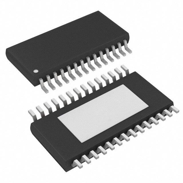
| 供应商器件封装 | 16-SOIC N |
| 其它名称 | 598-2312 |
| 内部驱动器 | 无 |
| 功率耗散 | 400 mW |
| 包装 | 散装 |
| 参考设计库 | http://www.digikey.com/rdl/4294959899/4294959898/1087 |
| 商标 | Cirrus Logic |
| 商标名 | CS1616 |
| 安装类型 | 表面贴装 |
| 安装风格 | SMD/SMT |
| 封装 | Tube |
| 封装/外壳 | 16-SOIC(0.154",3.90mm 宽) |
| 封装/箱体 | SOIC-16 |
| 工作温度 | -40°C ~ 125°C |
| 工作频率 | 6 kHz to 200 kHz |
| 工厂包装数量 | 48 |
| 恒压 | - |
| 恒流 | 是 |
| 拓扑 | 交直流离线开关,反激式,PWM,降压,升压 |
| 最大工作温度 | + 125 C |
| 最大电源电流 | 4.5 mA |
| 最小工作温度 | - 40 C |
| 标准包装 | 48 |
| 电压-电源 | 11 V ~ 17 V |
| 电压-输出 | - |
| 类型-初级 | 通用 |
| 类型-次级 | - |
| 系列 | CS1616 |
| 输入电压 | 11 V to 17 V |
| 输出数 | 1 |
| 配用 | /product-detail/zh/CRD1616-8W-Z/598-2309-ND/3854664 |
| 频率 | - |


- 商务部:美国ITC正式对集成电路等产品启动337调查
- 曝三星4nm工艺存在良率问题 高通将骁龙8 Gen1或转产台积电
- 太阳诱电将投资9.5亿元在常州建新厂生产MLCC 预计2023年完工
- 英特尔发布欧洲新工厂建设计划 深化IDM 2.0 战略
- 台积电先进制程称霸业界 有大客户加持明年业绩稳了
- 达到5530亿美元!SIA预计今年全球半导体销售额将创下新高
- 英特尔拟将自动驾驶子公司Mobileye上市 估值或超500亿美元
- 三星加码芯片和SET,合并消费电子和移动部门,撤换高东真等 CEO
- 三星电子宣布重大人事变动 还合并消费电子和移动部门
- 海关总署:前11个月进口集成电路产品价值2.52万亿元 增长14.8%


PDF Datasheet 数据手册内容提取
CS1615 CS1616 Single Stage Dimmable Offline AC/DC Controller for LED Lamps Features Overview • Best-in-class Dimmer Compatibility The CS1615 and CS1616 are high-performance single - Leading-edge (TRIAC) Dimmers stage dimmable offline AC/DC controllers. The CS1615/16 - Trailing-edge Dimmers is a cost-effective solution that provides unmatched single- - Digital Dimmers (Dimmers with an Integrated Power and multi-lamp dimmer-compatibility performance for Supply) dimmable LED applications. The CS1615 is designed for • Flicker-free Dimming 120VAC line voltage applications, and the CS1616 is • 0% to 100% Smooth Dimming designed for 230VAC line voltage applications. • Primary-side Regulation (PSR) Across a broad range of dimmers, the CS1615/16 provides • Active Power Factor Correction (PFC) smooth flicker free dimming, and consistently dims to - >0.9 Power Factor nearly zero light output, which closely matches the dimming • Constant-current Output performance of incandescent light bulbs. Cirrus Logic’s - Flyback patent pending approach to dimmer compatibility provides - Buck-boost full functionality on a wide range of dimmers, including • Tight LED Current Regulation: Better than ±5% leading-edge, trailing-edge, and digital dimmers. • Low THD: Less Than 20% • Up to 90% Efficiency Applications • Fast Startup • Retro-fit LED Lamps • IEC61000-3-2 Compliant • External LED Drivers • Meets NEMA SSL 6 Dimming Standard • LED Luminaries - Closely Matches Incandescent S-curve • Commercial Lighting • Protection Features - Output Open Circuit Ordering Information - Output Short Circuit See page 14. - External Overtemperature Using NTC L1 Vrect T1 D4 LED+ C6 R6 C5 R4 R5 C7 LED- D3 BR1 BR1 R2 Q1 D2 R3 IAC2 D5 VAUX 5 CS1615/16 GD13 Q3 R1 SOURCE MAaCins C1 C2 VAUX FBSENSE 11 R7 D1 Q2 FBAUX16 BR1 BR1 14 VDD eOTP10 C8 C3 C4 SGND CTRL1 CTRL2 GND RS Z1 4 8 9 12 RSense R8 NTC RCTRL1 RCTRL2 This document contains information for a product under development. Preliminary Product Information Cirrus Logic reserves the right to modify this product without notice. Cirrus Logic, Inc. Copyright Cirrus Logic, Inc. 2013 http://www.cirrus.com APR’13 (All Rights Reserved) DS961PP5
CS1615/16 1. INTRODUCTION VDD VDD 14 RVeoglutalagteo r 13 GD VZ VVDDDD((oonff)) +- POR 12 GND Blank 3 IAC 2 15k ADCIref OLP +- VOLP(th) OCP + - VOCP(th) SOURCE 5 VSOURCE(th) +- CPoenatrko l +- 11 FBSENSE DAC VPk_Max(th) - tVAUX + VFSTART(th) SGND 4 Output Overvoltage +- VOVP(th) CeTORTLP1 180 MUX ICONNECVTDD ZerDoe-ctuecrrtent +- VZCD(th) 16 FBAUX VDD CTRL2 9 VCONNECT(th) +- ICLAMP 3 CLAMP Figure 1. CS1615/16 Block Diagram A typical schematic using the CS1615/16 IC is shown on the The digital dual-mode controller is implemented with peak- previous page. current mode primary-side regulation, which eliminates the need Startup current is provided from a patent-pending, external, high- for additional components to provide feedback from the voltage source-follower network. In addition to providing startup secondary and reduces system cost and complexity. Voltage current, this unique topology is integral in providing compatibility across a user-selected resistor is sensed through pin FBSENSE with digital dimmers by ensuring V power is always available to control the peak current of the primary-side inductor. Leading- DD to the IC. During normal operation, an auxiliary winding on the edge and trailing-edge blanking on pin FBSENSE prevents false flyback transformer or buck-boost inductor back-biases the triggering. The required target LED current and average flyback source-follower circuit and provides steady-state operating transformer and buck-boost inductor input current are set by current to the IC to improve system efficiency. attaching resistors RCTRL1 and RCTRL2 on pins CTRL1 and CTRL2, respectively. The controller ensures half line-cycle Rectified input voltage V is sensed as a current into pin IAC rect averaged constant output current. and is used to control the adaptive dimmer-compatibility algorithm and to extract the phase of the input voltage for output Pin FBAUX is used for zero-current detection to ensure dimming control. The SOURCE pin is used to provide a control quasi-resonant switching of the single stage output. When an signal for the high-voltage source-follower circuit during Leading- external negative temperature coefficient (NTC) thermistor is connected to pin eOTP, the CS1615/16 monitors the system edge Mode and Trailing-edge Mode; it also provides the current temperature, allowing the controller to reduce the output current during startup. of the system. If the temperature reaches a designated high set point, the IC is shut down and stops switching. 2 DS961PP5
CS1615/16 2. PIN DESCRIPTION No Connect NC 1 16 FBAUX Zero-current Detect Rectifier Voltage Sense IAC 2 15 NC No Connect Voltage Clamp Current Source CLAMP 3 14 VDD IC Supply Voltage Source Ground SGND 4 13 GD Gate Drive Source Switch SOURCE 5 12 GND Ground No Connect NC 6 11 FBSENSE Flyback Current Sense No Connect NC 7 10 eOTP External Overtemperature Protection Dimmer Hold Current CTRL1 8 9 CTRL2 LED Load Current 16-lead SOIC and TSSOP Figure 2. CS1615/16 Pin Assignments Pin Name Pin # I/O Description NC 1 IN No Connect — Leave pin unconnected. Rectifier Voltage Sense — A current proportional to the rectified line voltage is fed IAC 2 IN into this pin. The current is measured with an A/D converter. Voltage Clamp Current Source — Connect to a voltage clamp circuit on the source- CLAMP 3 OUT switched dimmer-compatibility circuit. SGND 4 PWR Source Ground — Common reference current return for the SOURCE pin. Source Switch — Connected to the source of the source-switched external high-volt- SOURCE 5 IN age FET. NC 6 IN No Connect — Connect this pin to VDD using a 47k pull-up resistor. NC 7 IN No Connect — Connect this pin to VDD using a 47kpull-up resistor. Dimmer Hold Current — Connect a resistor to this pin to set the minimum input cur- CTRL1 8 IN rent being pulled by the flyback/buck-boost stage. CTRL2 9 IN LED Load Current — Connect a resistor to this pin to set the LED current. External Overtemperature Protection — Connect an external NTC thermistor to this eOTP 10 IN pin, allowing the internal A/D converter to sample the change to NTC resistance. Feedback Current Sense — The current flowing in the power FET is sensed across a FBSENSE 11 IN resistor. The resulting voltage is applied to this pin and digitized for use by the compu- tational logic to determine the FET's duty cycle. Ground — Common reference. Current return for both the input signal portion of the GND 12 PWR IC and the gate driver. GD 13 OUT Gate Drive — Gate drive for the power FET. IC Supply Voltage — Connect a storage capacitor to this pin to serve as a reservoir VDD 14 PWR for operating current for the device, including the gate drive current to the power tran- sistor. NC 15 - No Connect — Leave pin unconnected. Zero-current Detect — Connect to the flyback/buck-boost inductor auxiliary winding FBAUX 16 IN for demagnetization current zero-crossing detection. DS961PP5 3
CS1615/16 3. CHARACTERISTICS AND SPECIFICATIONS 3.1 Electrical Characteristics Typical characteristics conditions: Minimum/Maximum characteristics conditions: • T =25°C, V =12V, GND=0V • T =-40°Cto+125°C, V =11Vto17V, GND=0V A DD J DD • All voltages are measured with respect to GND. • Unless otherwise specified, all currents are positive when flowing into the IC. Parameter Condition Symbol Min Typ Max Unit VDD Supply Voltage Operating Range After Turn-on V 11 - 17 V DD Turn-on Threshold Voltage V Increasing V - 8.5 - V DD ST(th) Turn-off Threshold Voltage (UVLO) V Decreasing V - 7.5 - V DD STP(th) Zener Voltage (Note 1) IDD=20mA VZ 18.5 - 19.8 V VDD Supply Current Startup Supply Current V <V I - - 200 A DD ST(th) ST Operating Supply Current (Note 2) C =0.25nF, f 70kHz - 4.5 - mA L sw Reference Reference Current CS1615 V =200V I - 133 - A rect ref CS1616 Vrect=400V - 133 - A Zero-current Detect FBZCD Threshold V - 200 - mV FBZCD(th) FBZCD Blanking t - 2 - s FBZCB ZCD Sink Current (Note 3) IZCD -2 - - mA FBAUX Upper Voltage I =1mA - V +0.6 - V ZCD DD Current Sense Max Peak Control Threshold V - 1.4 - V Pk_Max(th) Leading-edge Blanking t - 550 - ns LEB Delay to Output - - 100 ns Pulse Width Modulator Minimum On Time - 0.55 - s Maximum On Time - 12.8 - s Minimum Switching Frequency t - 6 - kHz FB(Min) Maximum Switching Frequency t - 200 - kHz FB(Max) Gate Driver Output Source Resistance Z - 24 - OUT Output Sink Resistance Z - 11 - OUT Rise Time C =0.25nF - - 30 ns L Fall Time C =0.25nF - - 20 ns L 4 DS961PP5
CS1615/16 Parameter Condition Symbol Min Typ Max Unit Flyback/Buck-boost Protections Overcurrent Protection (OCP) (Note 4) VOCP(th) - 1.69 - V Overvoltage Protection (OVP) (Note 5) VOVP(th) - 1.25 - V Open Loop Protection (OLP) (Note 4) VOLP(th) - 200 - mV External Overtemperature Protection (eOTP) Pull-up Current Source – Maximum I - 80 - A CONNECT Conductance Accuracy (Note 6) - - ±5 Conductance Offset (Note 6) - ±250 - nS Current Source Voltage Threshold V - 1.25 - V CONNECT(th) Internal Overtemperature Protection (iOTP) Thermal Shutdown Threshold (Note 7) TSD - 135 - ºC Thermal Shutdown Hysteresis (Note 7) TSD(Hy) - 14 - ºC Notes: 1. The CS1615/16 has an internal shunt regulator that limits the voltage on the VDD pin. Shunt regulation voltage V is defined in Z the VDD Supply Voltage section on page4. 2. For test purposes, load capacitance C is connected to pin GD and is equal to 0.25nF. L 3. External circuitry should be designed to ensure that the ZCD current drawn from the internal clamp diode when it is forward biased does not exceed specification. 4. Protection is implemented using pin FBSENSE. See the CS1615/16 Block Diagram on page2. 5. Protection is implemented using pin FBAUX. See the CS1615/16 Block Diagram on page2 6. The conductance is specified in Siemens (S or 1/). Each LSB of the internal ADC corresponds to 250nS or one parallel 4M resistor. Full scale corresponds to 256 parallel 4M resistors or 15.625k. 7. Specifications are guaranteed by design and are characterized and correlated using statistical process methods. DS961PP5 5
CS1615/16 3.2 Thermal Resistance Symbol Parameter SOIC TSSOP Unit Junction-to-Ambient Thermal Impedance 2 Layer PCB 119 138 °C/W JA 4 Layer PCB 105 103 °C/W Junction-to-Case Thermal Impedance 2 Layer PCB 50 44 °C/W JC 4 Layer PCB 44 28 °C/W 3.3 Absolute Maximum Ratings Characteristics conditions: All voltages are measured with respect to GND. Pin Symbol Parameter Value Unit 14 V IC Supply Voltage 18.5 V DD 1,2,8,9, Analog Input Maximum Voltage -0.5 to (V +0.5) V 10,11,16 DD 1,2,8,9, Analog Input Maximum Current 5 mA 10,11,16 13 V Gate Drive Output Voltage -0.3 to (V +0.3) V GD DD 13 I Gate Drive Output Current -1.0 / +0.5 A GD 5 I Current into Pin 1.1 A SOURCE 3 I Clamp Output Current 15 mA CLAMP - P Total Power Dissipation 400 mW D - TJ Junction Temperature Operating Range (Note 8) -40 to +125 °C - T Storage Temperature Range -65 to +150 °C Stg Electrostatic Discharge Capability Human Body Model 2000 V All Pins ESD Charged Device Model 500 V Note: 8. Long-term operation at the maximum junction temperature will result in reduced product life. Derate internal power dissipation at the rate of 50mW/°C for variation over temperature. WARNING: Operation at or beyond these limits may result in permanent damage to the device. Normal operation is not guaranteed at these extremes. 6 DS961PP5
CS1615/16 4. TYPICAL PERFORMANCE PLOTS 8 3 6 2 s A) 4 si m ere (D Falling Edge yst ID 2 O H 1 Rising Edge L V 0 U 0 -2 -50 0 50 100 150 0 2 4 6 8 10 12 14 16 18 20 Temperature (ºC) V (V) DD Figure 3. UVLO Characteristics Figure 4. Supply Current vs. Voltage 10 20 19.5 9 VDD (V) Turn On V(V)z 19 8 Turn Off 18.5 7 -50 0 50 100 150 18 -45 -20 5 25 55 85 105 125 Temperature (ºC) Temperature (ºC) Figure 5. Turn On/Off Threshold Voltage vs. Temperature Figure 6. Zener Voltage vs. Temperature 0.25 35 30 -0.25 25 )(cid:159) -0.75 stance ( 1250 Source Drift (%) -1.25 si Re 10 Sink -1.75 5 0 -2.25 -43 25 125 -45 -20 5 25 55 85 105 125 Temperature (ºC) Temperature (°C) Figure 7. Gate Drive Resistance vs. Temperature Figure 8. Reference Current (I ) Drift vs. Temperature ref DS961PP5 7
CS1615/16 5. GENERAL DESCRIPTION detection algorithm uses the input line voltage slope and dimmer phase angle to determine the operating mode that matches the 5.1 Overview type of dimmer switch in the system. From there on, it periodically The CS1615 and CS1616 are high-performance single stage learns the dimmer type and can change the operating mode if the dimmable offline AC/DC controllers. The CS1615/16 is a cost- type of dimmer switch changes. effective solution that provides unmatched single- and multi-lamp 5.3.1.1 No-dimmer Mode dimmer-compatibility performance for dimmable LED If the CS1615/16 determines that the line is not phase cut by a applications. The CS1615 is designed for 120VAC line voltage dimmer switch, the IC operates the flyback/buck-boost in PFC applications, and the CS1616 is designed for 230VAC line mode to achieve a power factor greater than 0.9 while regulating voltage applications. the load current to a level set by resistor R . In addition, a CTRL2 The CS1615/16 features Cirrus Logic's proprietary adaptive No-dimmer Mode algorithm is applied to the source-controlled dimmer-compatibility algorithm that enables flicker-free operation dimmer-compatibility circuit for optimal performance, including from 0% to 100% output current with leading-edge dimmers, less than 20% of THD and highest possible overall efficiency. trailing-edge dimmers, and digital dimmers (dimmers with an integrated power supply). In addition, the CS1615/16 is configurable for isolated and non-isolated topologies. 5.2 IC Startup A high-voltage source-follower circuit is used to deliver startup current to the IC. During steady-state operation, an auxiliary winding on the transformer/inductor biases this circuit to an off state to improve system efficiency, and all IC supply current is provided from the auxiliary winding. The patent-pending technology of the high-voltage source-follower circuit enables system compatibility with digital dimmers (dimmers containing an internal power supply) by providing a continuous path for the Figure 9. No-dimmer Mode Waveform dimmer’s power supply to recharge during its off state. During steady-state operation, high-voltage FET Q1 in this circuit is source-controlled by a variable internal current source on the 5.3.1.2 Leading-edge Mode SOURCE pin to create the dimmer-compatibility circuit. A If the CS1615/16 determines that the line is phase cut by a Schottky diode with a forward voltage of less than 0.6V is leading-edge dimmer switch, the IC operates the flyback/buck- recommended for D1. Schottky diode D1 will limit inrush current boost in Dimmer Mode and the IC sets the dimmer firing current through the internal diode, preventing damage to the IC. as well as the attach current using a source-controlled dimmer- During initial power-up, the IC executes a fast startup algorithm, compatibility circuit for stable TRIAC dimmer operation. which drives the converter with peak currents that are above normal to charge the output capacitor. Once the output capacitor reaches a defined voltage, the IC drives the converter with nominal peak currents until normal operation is achieved. 5.3 IC Operation 5.3.1 Dimmer Detection The CS1615/16 dimmer switch detection algorithm determines if a non-dimming switch, a leading-edge dimmer switch, or a trailing-edge dimmer switch controls the solid-state lighting (SSL) system. For each type of switch, the IC uses a different operating mode: for a non-dimming switch, No-dimmer Mode is used; for a Figure 10. Leading-edge Mode Phase-cut Waveform leading-edge dimmer switch, Leading-edge Mode is used; for a trailing-edge dimmer switch, Trailing-edge Mode is used. As a 5.3.1.3 Trailing-edge Mode result, the overall performance is optimized in terms of power losses, efficiency, power factor, THD, and dimmer compatibility. If the CS1615/16 determines that the line is phase cut by a When the IC completes UVLO, it executes in Leading-edge trailing-edge dimmer switch, the IC operates the flyback/buck- Mode until the dimmer switch detection algorithm determines the boost in Dimmer Mode. The IC charges the capacitor in the appropriate operating mode for the IC. The dimmer switch 8 DS961PP5
CS1615/16 dimmer switch on the falling edge of the input voltage using a 5.4.1 Clamp Overpower Protection source-controlled dimmer-compatibility circuit. The CS1615/16 clamp overpower protection (COP) control logic averages the ‘ON’ time of the clamp circuit. If the output of the averaging logic exceeds 10%, a COP event is actuated. The clamp circuit is disabled as well as the flyback/buck-boost controller and the dimmer-compatibility circuit. The COP fault state is not cleared until the power to the IC is recycled. 5.5 Dimmer Angle Extraction and the Dim Mapping Algorithm When operating with a dimmer, the dimming signal is extracted in the time domain and is proportional to the conduction angle of the dimmer. A control variable is passed to the quasi-resonant flyback/buck-boost controller to achieve a wide range of output Figure 11. Trailing-edge Mode Phase-cut Waveform currents. 5.6 Dual-mode Flyback/Buck-boost 5.3.2 Switch Overpower Protection The CS1615/16 is configurable for isolated or non-isolated To prevent excessive power dissipation on the source-switched topologies using a flyback transformer or buck-boost inductor, FET Q1, the CS1615/16 monitors voltage across Q1 and current respectively. The CS1615/16 controls the dual-mode flow through Q1 to calculate average power dissipation. If the flyback/buck-boost to satisfy the dimmer hold current calculated power exceeds the overpower protection threshold a requirement in Dimmer Mode and provide power factor fault condition occurs. The IC output is disabled and the correction in No-dimmer Mode. The dual-mode ensures a controller attempts to restart after approximately thirty seconds. minimum average input current greater than the required dimmer 5.4 Voltage Clamp Circuit hold current when behind a dimmer and shapes the line current when not behind a dimmer to provide power factor correction. It To keep trailing-edge dimmer switches conducting and from also ensures half line-cycle averaged constant output current. misfiring, the dimmer switch internal capacitor has to be Figure13 illustrates the dual-mode flyback topology. The charged quickly around the trailing edge of the phase-cut CS1615/16 regulates output current using primary-side control, waveform. In addition to the dimmer compatible circuit, an which eliminates the need for opto-coupler feedback. The control optional clamp circuit provides a high-current sinking path for loop operates in peak current control mode. Demagnetization delivering the required amount of charge onto the dimmer time of the transformer is sensed by the FBAUX pin using an switch capacitor in a short amount of time. auxiliary winding and is used as an input to the control loop. The CS1615/16 provides active clamp circuitry on the CLAMP pin, as shown in Figure12. Vrect T1 Vrect T1 D4 LED+ C6 R6 C6 R6 C7 R4 D3 LED- D3 D5 R5 CS1615/16 VAUX 2 RClamp GD13 Q3 VDD IAC R7 ICLAMP Q FBSENSE 11 FBAUX16 C8 S1 CLAMP3 GD13 Q3 1G2ND CT9RL2 RSense R8 CS1615/16 RCTRL2 RSense Figure 13. Flyback Model Figure 12. CLAMP Pin Model DS961PP5 9
CS1615/16 Figure14 illustrates the dual-mode buck-boost topology. The the target output charge is achieved every half line-cycle, thus CS1615/16 regulates the output current by controlling the peak regulating the output current. current to ensure that the target output charge is achieved every 5.6.3 Input Current Shaping half line-cycle. Demagnetization time of the inductor is sensed by the FBAUX pin using an auxiliary winding and is used as an input The CS1615/16 shapes the input current by controlling the peak to the control loop. primary current and the flyback/buck-boost switching frequency. It shapes the currents differently when behind a dimmer Vrect LED- compared to when not behind a dimmer. 5.6.3.1 Operation Behind a Dimmer L2 C7 Operating behind a dimmer, the CS1615/16 controls the D4 switching frequency to ensure that the average input current is LED+ greater than the dimmer hold current requirement. The dimmer CS1615/16 hold current level is sensed using resistor R on pin CTRL1, CTRL1 which is sampled periodically by an ADC. The value of this GD13 Q3 R7 D5 resistor can be determined using the formula shown in FBSENSE 11 VAUX Equation2. 16 FBAUX 1.4V4M GND CTRL2 RSense R8 C8 RCTRL1 = 5----1---1----------I--I-N------C----C-----------R-----S---e---n---s---e-- [Eq.2] 12 9 RCTRL2 where, I =constant input current used when designing circuit Figure 14. Buck-boost Model IN(CC) R =resistor attached to pin FBSENSE Sense 5.6.1 Primary-Side Current Control 5.6.3.2 Operation in No-dimmer Mode All input current shaping and output power transfer is attained Operating in No-dimmer Mode, the CS1615/16 controls the using a peak current control algorithm. Demagnetization time of switching frequency to ensure that the average input current the primary inductor is sensed by the FBAUX pin using an follows the line voltage to provide power factor correction. In No- auxiliary winding and is used as an input to the control algorithm. dimmer Mode the controller is designed to operate in quasi- The values obtained from R and R are the other CTRL1 CTRL2 resonant mode to improve efficiency. inputs to the control algorithm that help shape the input current 5.6.4 Max Primary-side Switching Current and control the LED current, respectively. 5.6.2 Output Current Regulation Maximum primary-side switching current IPK(max) is set using resistor R connected to pin FBSENSE of the CS1615/16. Sense The CS1615/16 regulates output current by controlling the The maximum primary-side switching current can be calculated charge transferred over a half line-cycle. The full-scale output using Equation3. current target is set using resistor R , which is connected on CTRL2 1.4 pin CTRL2. This pin is sampled periodically by an ADC. The I = ------------------- [Eq.3] PKmax R value of this resistor can be determined using Equation1. Sense 5.6.5 Auxiliary Winding Configuration 1.4VN4M R = ------------------------------------------------------------------------ [Eq.1] CTRL2 1.25511R I The auxiliary winding is used for zero-current detection (ZCD), Sense OUT overvoltage protection (OVP), fast startup, and the steady-state power supply. The voltage on the auxiliary winding is sensed where, through pin FBAUX of the CS1615/16 for zero-current detection, N=turns ratio overvoltage protection, and fast startup. The auxiliary winding is also used to provide the steady-state power supply to the I =current through LED at maximum output OUT CS1615/16. R =resistor attached to pin FBSENSE Sense 5.6.6 Output Open Circuit Protection When designing a buck-boost topology the turns ratio N is set to one. Output open circuit protection and output overvoltage protection (OVP) are implemented by monitoring the output voltage through The CS1615/16 uses the value obtained from the resistor along the transformer auxiliary winding. If the voltage on the FBAUX pin with the phase-cut and line-cycle period information to determine exceeds a threshold V of 1.25V, a fault condition occurs. the corresponding target full-scale output charge. The IC controls OVP(th) The IC output is disabled and the controller attempts to restart the inductor switching frequency and peak current to ensure that after approximately one second. 10 DS961PP5
CS1615/16 5.6.7 Overcurrent Protection scale down the internal dim level of the system (and hence LED current I ) if the temperature exceeds 95°C. The large time Overcurrent protection (OCP) is implemented by monitoring the LED constant for this filter ensures that the dim scaling does not voltage across the sense resistor. If this voltage exceeds a happen spontaneously and is not noticeable (suppress spurious threshold V of 1.69V, a fault condition occurs. The IC OCP(th) glitches). The eOTP tracking circuit is designed to function output is disabled and the controller attempts to restart after accurately with external capacitance up to 470pF. approximately one second. The tracking range of this resistance ADC is approximately 5.6.8 Open Loop Protection 15.5k to 4M. The series resistor R is used to adjust the S Open loop protection (OLP) and sense resistor short protection resistance of the NTC to fall within the ADC tracking range, are implemented by monitoring the voltage across the resistor. If allowing the entire dynamic range of the ADC to be well used. the voltage on pin FBSENSE does not reach the protection The CS1615/16 recognizes a resistance (RS+RNTC) equal to threshold V of 200mV, the IC output is disabled, and the 20.3kwhich corresponds to a temperature of 95°C, as the OLP(th) controller attempts to restart after approximately one second. beginning of an overtemperature dimming event and starts reducing the power dissipation. The output current is scaled until 5.7 Overtemperature Protection the series resistance (R +R ) value reaches 16.26k S NTC The CS1615/16 incorporates internal overtemperature (125°C). Beyond this temperature, the IC shuts down until the protection (iOTP) and the ability to connect an external resistance (RS+RNTC) rises above 19.23k. This is not a latched overtemperature sense circuit for IC protection. Typically, an protection state, and the ADC keeps tracking the temperature in NTC thermistor is used. this state in order to clear the fault state once the temperature drops below 110°C. 5.7.1 Internal Overtemperature Protection When exiting reset, the chip enters startup and the ADC quickly Internal overtemperature protection (iOTP) is activated, and (<5ms) tracks the external temperature to check if it is below the switching is disabled when the die temperature of the devices 110°C reference code before the controller is powered up. If this exceeds 135°C. There is a hysteresis of about 14°C before check fails, the chip will wait until this condition becomes true resuming normal operation. before initializing the rest of the system. 5.7.2 External Overtemperature Protection For example, a 14k (±1% tolerance) series resistor is required to allow measurements of up to 130°C to be within the eOTP The external overtemperature protection (eOTP) pin is used to tracking range when a 100k NTC with a Beta of 4275. If the implement overtemperature protection. A negative temperature temperature exceeds 95°C, thermistor R is approximately coefficient (NTC) thermistor resistive network is connected to pin NTC 6.3k and series resistor R is 14k, so the eOTP pin has a total eOTP, usually in the form of a series combination of a resistor R S S resistance of 20.3k. The eOTP pin initiates protective dimming and a thermistor R (see Figure15). The CS1615/16 cyclically NTC action by reducing the power dissipation. At 125°C the thermistor samples the resistance connected to pin eOTP. R has 2.26k plus a series resistor R equal to 14k present NTC S CS1615/16 V a resistance of 16.26k at the eOTP pin reaching the point where DD a thermal shutdown fault intervenes. The CS1615/16 will eOTP ICONNECT continue to monitor pin eOTP and once the series resistor RS Control Comp_Out +- V eOTP10 rpelussu mthee p tohweremr cisotonrv eRrsNiToCn (rsiseees Faigbuorvee 1169).. 23k the device will CONNECT(th) RS NTC (COpNtiTonCal) m.) 100% o N , D Figure 15. eOTP Functional Diagram E L (I 50% The total resistance on the eOTP pin gives an indication of the nt temperature and is used in a digital feedback loop to adjust e rr current I into the NTC and series resistor R to maintain u CONNECT S C a constant reference voltage V of 1.25V. Current 0 CONNECT(th) 25 95 125 I is generated from a controlled current source with a CONNECT Temperature (°C) full-scale current of 80A. When the loop is in equilibrium, the voltage on the eOTP pin fluctuates around V . A Figure 16. eOTP Temperature vs. Impedance CONNECT(th) resistance ADC is used to generate I . The ADC output CONNECT If the external overtemperature protection feature is not required, is filtered to suppress noise and compared against a reference connect the eOTP pin to GND using a 50k-to-500k resistor to that corresponds to 125°C. A second low-pass filter with a time disable the eOTP feature. constant of two seconds filters the ADC output and is used to DS961PP5 11
CS1615/16 6. PACKAGE DRAWING 16-PIN TSSOP (173 MIL BODY) (cid:18)(cid:23) (cid:70) (cid:35) (cid:38)(cid:18) (cid:38) (cid:17)(cid:15)(cid:19)(cid:22) (cid:40)(cid:34)(cid:54)(cid:40)(cid:38)(cid:1)(cid:49)(cid:45)(cid:34)(cid:47)(cid:38) (cid:49)(cid:42)(cid:47)(cid:1)(cid:18) (cid:84) (cid:45) (cid:37)(cid:38)(cid:53)(cid:34)(cid:42)(cid:45)(cid:1)(cid:34) (cid:42)(cid:47)(cid:37)(cid:42)(cid:36)(cid:34)(cid:53)(cid:48)(cid:51) (cid:19)(cid:89)(cid:1)(cid:25)(cid:1)(cid:53)(cid:74)(cid:81)(cid:84) (cid:18) (cid:19) (cid:69)(cid:69)(cid:69)(cid:36)(cid:35)(cid:34) (cid:53)(cid:48)(cid:49)(cid:1)(cid:55)(cid:42)(cid:38)(cid:56) (cid:37) (cid:37)(cid:38)(cid:53)(cid:34)(cid:42)(cid:45)(cid:1)(cid:34) (cid:34) (cid:34) (cid:68) (cid:52)(cid:38)(cid:34)(cid:53)(cid:42)(cid:47)(cid:40)(cid:1)(cid:49)(cid:45)(cid:34)(cid:47)(cid:38) (cid:34)(cid:18) (cid:67) (cid:18)(cid:23)(cid:89) (cid:18)(cid:23)(cid:89) (cid:36) (cid:66)(cid:66)(cid:66)(cid:36) (cid:67)(cid:67)(cid:67) (cid:36)(cid:35)(cid:34) (cid:38)(cid:47)(cid:37)(cid:1)(cid:55)(cid:42)(cid:38)(cid:56) (cid:52)(cid:42)(cid:37)(cid:38)(cid:1)(cid:55)(cid:42)(cid:38)(cid:56) mm inch Dimension MIN NOM MAX MIN NOM MAX A - - - - 1.20 - - - - 0.047 A1 0.05 - - 0.15 0.002 - - 0.006 b 0.19 - - 0.30 0.007 - - 0.012 C 0.09 - - 0.20 0.004 - - 0.008 D 4.90 5.00 5.10 0.193 0.197 0.201 E 6.40 BSC 0.252 BSC E1 4.30 4.40 4.50 0.169 0.173 0.177 e 0.65 BSC 0.026 BSC L 0.45 0.60 0.75 0.018 0.024 0.030 Θ 0° - - 8° 0° - - 8° aaa 0.10 0.004 bbb 0.10 0.004 ddd 0.20 0.008 1. Controlling dimensions are in millimeters. 2. Dimensioning and tolerances per ASME Y14.5M. 3. This drawing conforms to JEDEC outline MO-153, variation AB. 4. Recommended reflow profile is per JEDEC/IPC J-STD-020. 12 DS961PP5
CS1615/16 16-PIN SOICN (150 MIL BODY) mm inch Dimension MIN NOM MAX MIN NOM MAX A - - - - 1.75 - - - - 0.069 A1 0.10 - - 0.25 0.004 - - 0.010 b 0.31 - - 0.51 0.012 - - 0.020 c 0.10 - - 0.25 0.004 - - 0.010 D 9.90 BSC 0.390 BSC E 6.00 BSC 0.236 BSC E1 3.90 BSC 0.154 BSC e 1.27 BSC 0.050 BSC L 0.40 - - 1.27 0.016 - - 0.050 Θ 0° - - 8° 0° - - 8° aaa 0.10 0.004 bbb 0.25 0.010 ddd 0.25 0.010 Notes: 1. Controlling dimensions are in millimeters. 2. Dimensions and tolerances per ASME Y14.5M. 3. This drawing conforms to JEDEC outline MS-012, variation AC for standard 16 SOICN narrow body. 4. Recommended reflow profile is per JEDEC/IPC J-STD-020. DS961PP5 13
CS1615/16 7. ORDERING INFORMATION Ordering Number Container AC Line Voltage Temperature Package CS1615-FSZ Bulk 120VAC -40 °C to +125 °C 16-lead SOICN, Lead (Pb) Free CS1615-FSZR Tape & Reel CS1616-FSZ Bulk 230VAC -40 °C to +125 °C 16-lead SOICN, Lead (Pb) Free CS1616-FSZR Tape & Reel CS1615-FZZ Bulk 120VAC -40 °C to +125 °C 16-lead TSSOP, Lead (Pb) Free CS1615-FZZR Tape & Reel CS1616-FZZ Bulk 230VAC -40 °C to +125 °C 16-lead TSSOP, Lead (Pb) Free CS1616-FZZR Tape & Reel 8. ENVIRONMENTAL, MANUFACTURING, & HANDLING INFORMATION Part Number Peak Reflow Temp MSL Ratinga Max Floor Lifeb CS1615-FSZ 260 °C 3 7 Days CS1616-FSZ 260 °C 3 7 Days CS1615-FZZ 260 °C 3 7 Days CS1616-FZZ 260 °C 3 7 Days a.MSL (Moisture Sensitivity Level) as specified by IPC/JEDEC J-STD-020. b.Stored at 30°C, 60% relative humidity. 14 DS961PP5
CS1615/16 REVISION HISTORY Revision Date Changes T1 JUN 2012 Initial release. PP1 JUL 2012 Corrected typographical errors. PP2 SEP 2012 Clarified context and corrected typographical errors. PP3 OCT 2012 Clarified context. PP4 JAN 2013 Buck-boost content added, and clarified context. PP5 APR 2013 Context clarification. DS961PP5 15
CS1615/16 Contacting Cirrus Logic Support For all product questions and inquiries contact a Cirrus Logic Sales Representative. To find the one nearest to you go to www.cirrus.com IMPORTANT NOTICE “Preliminary” product information describes products that are in development and subject to development changes. Cirrus Logic, Inc. and its subsidiaries ("Cirrus") believe that the information contained in this document is accurate and reliable. However, the information is subject to change without notice and is provided "AS IS" without warranty of any kind (express or implied). Customers are advised to obtain the latest version of relevant information to verify, before placing orders, that information being relied on is current and complete. All products are sold subject to the terms and conditions of sale supplied at the time of order acknowledgment, including those pertaining to warranty, indemnification, and limitation of liability. No responsibility is assumed by Cirrus for the use of this information, including use of this information as the basis for manufacture or sale of any items, or for infringement of patents or other rights of third parties. This document is the property of Cirrus and by furnishing this information, Cirrus grants no license, express or implied under any patents, mask work rights, copyrights, trademarks, trade secrets or other intellectual property rights. Cirrus owns the copyrights associated with the information contained herein and gives consent for copies to be made of the information only for use within your organization with respect to Cirrus integrated circuits or other products of Cirrus. This con- sent does not extend to other copying such as copying for general distribution, advertising or promotional purposes, or for creating any work for resale. CERTAIN APPLICATIONS USING SEMICONDUCTOR PRODUCTS MAY INVOLVE POTENTIAL RISKS OF DEATH, PERSONAL INJURY, OR SEVERE PROP- ERTY OR ENVIRONMENTAL DAMAGE ("CRITICAL APPLICATIONS"). CIRRUS PRODUCTS ARE NOT DESIGNED, AUTHORIZED OR WARRANTED FOR USE IN PRODUCTS SURGICALLY IMPLANTED INTO THE BODY, AUTOMOTIVE SAFETY OR SECURITY DEVICES, LIFE SUPPORT PRODUCTS OR OTHER CRITICAL APPLICATIONS. INCLUSION OF CIRRUS PRODUCTS IN SUCH APPLICATIONS IS UNDERSTOOD TO BE FULLY AT THE CUSTOMER'S RISK AND CIRRUS DISCLAIMS AND MAKES NO WARRANTY, EXPRESS, STATUTORY OR IMPLIED, INCLUDING THE IMPLIED WARRANTIES OF MERCHANT- ABILITY AND FITNESS FOR PARTICULAR PURPOSE, WITH REGARD TO ANY CIRRUS PRODUCT THAT IS USED IN SUCH A MANNER. IF THE CUSTOMER OR CUSTOMER'S CUSTOMER USES OR PERMITS THE USE OF CIRRUS PRODUCTS IN CRITICAL APPLICATIONS, CUSTOMER AGREES, BY SUCH USE, TO FULLY INDEMNIFY CIRRUS, ITS OFFICERS, DIRECTORS, EMPLOYEES, DISTRIBUTORS AND OTHER AGENTS FROM ANY AND ALL LIABILITY, IN- CLUDING ATTORNEYS' FEES AND COSTS, THAT MAY RESULT FROM OR ARISE IN CONNECTION WITH THESE USES. Use of the formulas, equations, calculations, graphs, and/or other design guide information is at your sole discretion and does not guarantee any specific results or performance. The formulas, equations, graphs, and/or other design guide information are provided as a reference guide only and are intended to assist but not to be solely relied upon for design work, design calculations, or other purposes. Cirrus Logic makes no representations or warranties concerning the formulas, equa- tions, graphs, and/or other design guide information. Cirrus Logic, Cirrus, the Cirrus Logic logo designs, EXL Core, and the EXL Core logo design are trademarks of Cirrus Logic, Inc. All other brand and product names in this document may be trademarks or service marks of their respective owners. 16 DS961PP5