ICGOO在线商城 > 射频/IF 和 RFID > RF 评估和开发套件,板 > CGHV14250F-TB
 Datasheet下载
- 型号: CGHV14250F-TB
- 制造商: Cree
- 库位|库存: xxxx|xxxx
- 要求:
| 数量阶梯 | 香港交货 | 国内含税 |
| +xxxx | $xxxx | ¥xxxx |
查看当月历史价格
查看今年历史价格
CGHV14250F-TB产品简介:
ICGOO电子元器件商城为您提供CGHV14250F-TB由Cree设计生产,在icgoo商城现货销售,并且可以通过原厂、代理商等渠道进行代购。 CGHV14250F-TB价格参考¥4051.33-¥4051.33。CreeCGHV14250F-TB封装/规格:RF 评估和开发套件,板, 。您可以下载CGHV14250F-TB参考资料、Datasheet数据手册功能说明书,资料中有CGHV14250F-TB 详细功能的应用电路图电压和使用方法及教程。
型号为CGHV14250F-TB的开发套件由品牌Cree(现为Wolfspeed)生产,属于射频(RF)评估和开发套件类别。该套件主要用于评估和开发基于碳化硅(SiC)和氮化镓(GaN)技术的高功率射频功率晶体管,特别适用于需要高效率和高功率密度的应用场景。

其主要应用场景包括:

1. 无线通信基础设施:如4G/5G基站、宏蜂窝和小蜂窝基站中的功率放大器设计与测试。
2. 广播系统:用于FM和TV广播发射机中的高功率放大模块开发。
3. 工业加热与等离子体生成:用于射频能量应用,如材料加工、感应加热和等离子体发生器。
4. 雷达与国防通信:适用于军用雷达、电子战系统和高可靠性通信设备中的高功率射频放大器设计。
5. 测试与测量设备:用于射频测试系统中,作为高功率放大模块的评估平台。

该评估板为工程师提供了方便的测试环境,支持性能验证、热管理评估和电路匹配优化,有助于加快产品开发周期并提升系统性能。
| 参数 | 数值 |
| 产品目录 | |
| 描述 | TEST FIXTURE FOR CGHV14250 |
| 产品分类 | |
| 品牌 | Cree Inc |
| 数据手册 | |
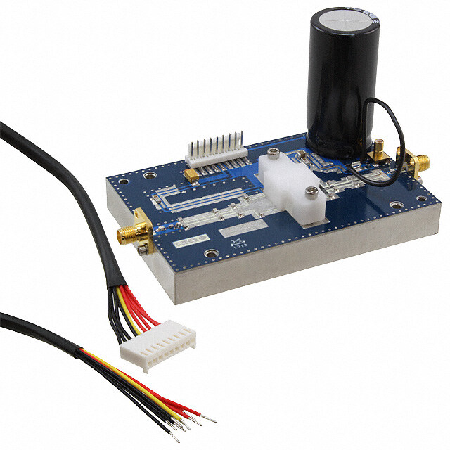
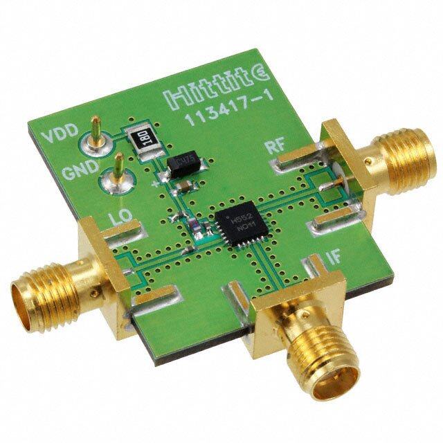
| 产品图片 |
|
| 产品型号 | CGHV14250F-TB |
| rohs | 无铅 / 符合限制有害物质指令(RoHS)规范要求 |
| 产品系列 | - |
| 所含物品 | 板 |
| 标准包装 | 1 |
| 类型 | FET |
| 配套使用产品/相关产品 | CGHV14250 |
| 频率 | 1.2GHz ~ 1.4GHz |


- 商务部:美国ITC正式对集成电路等产品启动337调查
- 曝三星4nm工艺存在良率问题 高通将骁龙8 Gen1或转产台积电
- 太阳诱电将投资9.5亿元在常州建新厂生产MLCC 预计2023年完工
- 英特尔发布欧洲新工厂建设计划 深化IDM 2.0 战略
- 台积电先进制程称霸业界 有大客户加持明年业绩稳了
- 达到5530亿美元!SIA预计今年全球半导体销售额将创下新高
- 英特尔拟将自动驾驶子公司Mobileye上市 估值或超500亿美元
- 三星加码芯片和SET,合并消费电子和移动部门,撤换高东真等 CEO
- 三星电子宣布重大人事变动 还合并消费电子和移动部门
- 海关总署:前11个月进口集成电路产品价值2.52万亿元 增长14.8%


PDF Datasheet 数据手册内容提取
CGHV14250 250 W, 1200 - 1400 MHz, GaN HEMT for L-Band Radar Systems Cree’s CGHV14250 is a gallium nitride (GaN) high electron mobility transistor (HEMT) designed specifically with high efficiency, high gain and wide bandwidth capabilities, which makes the CGHV14250 ideal for 1.2 - 1.4 GHz L-Band radar amplifier applications. The transistor could be utilized for band specific applications ranging from 900 through 1800 MHz. The package options are ceramic/metal flange and pill package. P PNa: cCkGaHgeV 1T4y2p5e:0 4F,4 C0G16H2V, 1444205106P1 Typical Performance Over 1.2-1.4 GHz (T = 25˚C) of Demonstration Amplifier C Parameter 1.2 GHz 1.25 GHz 1.3 GHz 1.35 GHz 1.4 GHz Units Output Power 365 365 350 310 330 W Gain 18.6 18.6 18.4 17.9 18.2 dB Drain Efficiency 80 80 77 74 76 % Note: Measured in the CGHV14250-AMP amplifier circuit, under 500 μs pulse width, 10% duty cycle, P = 37 dBm. IN Features • Reference design amplifier 1.2 - 1.4 GHz Operation • FET Tuning range UHF through 1800 MHz • 330 W Typical Output Power • 18 dB Power Gain 5 1 0 • 77% Typical Drain Efficiency 2 r e • <0.3 dB Pulsed Amplitude Droop b m ec • Internally pre-matched on input, unmatched output e D – 1 .1 v e R Subject to change without notice. 1 www.cree.com/rf
Absolute Maximum Ratings (not simultaneous) Parameter Symbol Rating Units Conditions Drain-Source Voltage V 125 Volts 25˚C DSS Gate-to-Source Voltage V -10, +2 Volts 25˚C GS Storage Temperature T -65, +150 ˚C STG Operating Junction Temperature T 225 ˚C J Maximum Forward Gate Current I 42 mA 25˚C GMAX Maximum Drain Current1 I 18 A 25˚C DMAX Soldering Temperature2 T 245 ˚C S Screw Torque τ 40 in-oz CW Thermal Resistance, Junction to Case3 R 0.95 ˚C/W P = 167 W, 65˚C θJC DISS Pulsed Thermal Resistance, Junction to Case3 R 0.57 ˚C/W P = 167 W, 500 µsec, 10%, 85˚C θJC DISS Pulsed Thermal Resistance, Junction to Case4 R 0.63 ˚C/W P = 167 W, 500 µsec, 10%, 85˚C θJC DISS Case Operating Temperature5 T -40, +130 ˚C P = 167 W, 500 µsec, 10% C DISS Note: 1 Current limit for long term, reliable operation 2 Refer to the Application Note on soldering at http://www.cree.com/rf/document-library 3 Measured for the CGHV14250P 4 Measured for the CGHV14250F 5 See also, the Power Dissipation De-rating Curve on Page 5 Electrical Characteristics Characteristics Symbol Min. Typ. Max. Units Conditions DC Characteristics1 (T = 25˚C) C Gate Threshold Voltage V -3.8 -3.0 -2.3 V V = 10 V, I = 41.8 mA GS(th) DC DS D Gate Quiescent Voltage V – -2.7 – V V = 50 V, I = 500 mA GS(Q) DC DS D Saturated Drain Current2 I 31.4 37.6 – A V = 6.0 V, V = 2.0 V DS DS GS Drain-Source Breakdown Voltage V 150 – – V V = -8 V, I = 41.8 mA BR DC GS D RF Characteristics3 (T = 25˚C, F = 1.3 GHz unless otherwise noted) C 0 Output Power P 275 330 – W V = 50 V, I = 500 mA, P = 37 dBm OUT DD DQ IN Drain Efficiency D 63 77 – % V = 50 V, I = 500 mA, P = 37 dBm E DD DQ IN Power Gain G – 18.2 – dB V = 50 V, I = 500 mA, P = 37 dBm P DD DQ IN Pulsed Amplitude Droop D – -0.3 – dB V = 50 V, I = 500 mA DD DQ No damage at all phase angles, Output Mismatch Stress VSWR – 5 : 1 – Y V = 50 V, I = 500 mA, P = 37 dBm Pulsed DD DQ IN Dynamic Characteristics Input Capacitance C – 150 – pF V = 50 V, V = -8 V, f = 1 MHz GS DS gs Output Capacitance C – 16 – pF V = 50 V, V = -8 V, f = 1 MHz DS DS gs Feedback Capacitance C – 1.35 – pF V = 50 V, V = -8 V, f = 1 MHz GD DS gs Notes: 1 Measured on wafer prior to packaging. 2 Scaled from PCM data. 3 Measured in CGHV14250-AMP. Pulse Width = 500 μS, Duty Cycle = 10%. Cree, Inc. 4600 Silicon Drive Copyright © 2014-2015 Cree, Inc. All rights reserved. The information in this document is subject to change without notice. Cree and the Cree logo are Durham, North Carolina, USA 27703 registered trademarks of Cree, Inc. USA Tel: +1.919.313.5300 Fax: +1.919.869.2733 2 CGHV14250 Rev 1.1 www.cree.com/rf
Typical Performance Figure 1. - CGHV14250 Typical Sparameters CGHV14250TypicalSparameters Tcase = 25°C V = 50 V, I = 500 mA Vdd=D5D0V,Idq=D5Q00mA 30 20 10 B)B) dd (( 0 ee dd uu nitnit gg--1100 aa MM -20 S(2,1) -30 S(1,1) S(2,2) -40 1 1.1 1.2 1.3 1.4 1.5 1.6 Frequency(GHz) Figure 2. - CGHV14250 Typical RF Results CGHV14250TypicalRFResults V = 50 V, I = 500 mA, P = 37 dBm DVDdd=50V,DIQdq=500mA,PIiNn=37dBm TcTacsaes e== 2255°Cde, gPCu,lsPeu lWseidWthid =th 5=0500 0µsu,s D,Duutyty CCyyccllee == 1100 %% 450 90 Drain Efficiency 400 80 350 70 %)%) (( W)W) 30D0rain Efficiency Output Power 60 ncyncy r(r( Output Power ciecie wewe 250 OutputPower 50 EffiEffi oo PP nn utut Gain rairai pp 200 40 DD utut DrainEfficiency && OO B)B) 150 30 dd GGaianin (( Gain Gain nn aiai 100 20 GG 50 10 0 0 1.10 1.15 1.20 1.25 1.30 1.35 1.40 1.45 1.50 Frequency(GHz) Cree, Inc. 4600 Silicon Drive Copyright © 2014-2015 Cree, Inc. All rights reserved. The information in this document is subject to change without notice. Cree and the Cree logo are Durham, North Carolina, USA 27703 registered trademarks of Cree, Inc. USA Tel: +1.919.313.5300 Fax: +1.919.869.2733 3 CGHV14250 Rev 1.1 www.cree.com/rf
Typical Performance Figure 3. - CGHV14250 Typical RF Results CGHV14250TypicalRFResults V = 50 V, I = 500 mA, P = 37 dBm VdDDd=50V,IdDQq=500mA,PinIN=37dBm TTccaassee= =8 855d°eCg, CP,uPlsuels WeWiditdht h= =505000 µuss,, DDuuttyy CCyyccllee == 1100% % 400 80 Drain Efficiency 350 70 300 60 %)%) (( Output Power yy W)W) ncnc ower(ower( 250 OGuaitnputPower 50 EfficieEfficie PP nn putput 200 DrainEfficiency 40 DraiDrai utut && OO 150 30 B)B) dd Gain (( nn 100 20 aiai GG 50 10 0 0 1.10 1.15 1.20 1.25 1.30 1.35 1.40 1.45 1.50 Frequency(GHz) Figure 4. - CGHV14250 CW RF Results V = 50 V, I C G= H5V0104 m25A0F, PCW =R 3F7R deBsmult,s Tcase = 65°C DD DQ IN Vdd=50V,Idq=500mA,Pin=37dBm,Tcase=65C 350 70 Drain Efficiency 300 60 %)%) (( 250 50 yy cc nn W)W) Output Power ciecie er(er( 200 40 EffiEffi ww PoPo ainain rr utut DD pp 150 30 dd OutOut anan Gain B)B) dd 100 20 (( nn aiai GG 50 Pout 10 Gain DrainEff 0 0 1.10 1.15 1.20 1.25 1.30 1.35 1.40 1.45 1.50 Frequency(GHz) Cree, Inc. 4600 Silicon Drive Copyright © 2014-2015 Cree, Inc. All rights reserved. The information in this document is subject to change without notice. Cree and the Cree logo are Durham, North Carolina, USA 27703 registered trademarks of Cree, Inc. USA Tel: +1.919.313.5300 Fax: +1.919.869.2733 4 CGHV14250 Rev 1.1 www.cree.com/rf
Source and Load Impedances D Z Source Z Load G S Frequency (MHz) Z Source Z Load 900 0.6 - j0.3 5.3 + j0.1 1000 0.7 - j0.8 4.3 +j0.8 1100 1.3 - j1.1 3.3 + j0.8 1200 1.8 - j1.1 3.0 + j0.4 1300 2.5 - j0.7 2.5 + j0.4 1400 3.4 - j0.7 2.3 + j0.1 1500 1.8 - j0.9 2.3 + j0 Note 1. V = 50 V, I = 500 mA in the 440162 package DD DQ Note 2. Optimized for power gain, P and Drain Efficiency SAT Note 3. When using this device at low frequency, series resistors should be used to maintain amplifier stability CGHV14250F Power Dissipation De-rating Curve Figure 4. - CGHV14250 Transient Power Dissipation De-Rating Curve CGHV14250TransientPowerDissipationDe-RatingCurve 180 Pill - 500 µs 10% 160 140 120 W)W) Flange - CW (( nn oo 100 atiati pp DissiDissi 80 Note 1 erer ww oo 60 PP Flange-500us10% 40 Pill-500us10% Flange-1ms-20% 20 Pill-1ms-20% 0 0 25 50 75 100 125 150 175 200 225 250 MaximumCaseTemperature(°C) Note 1. Area exceeds Maximum Case Temperature (See Page 2). Cree, Inc. 4600 Silicon Drive Copyright © 2014-2015 Cree, Inc. All rights reserved. The information in this document is subject to change without notice. Cree and the Cree logo are Durham, North Carolina, USA 27703 registered trademarks of Cree, Inc. USA Tel: +1.919.313.5300 Fax: +1.919.869.2733 5 CGHV14250 Rev 1.1 www.cree.com/rf
CGHV14250-AMP Demonstration Amplifier Circuit Bill of Materials Designator Description Qty R1 RES, 1/16W, 0603, 1%, 562 OHMS 1 R2 RES, 5.1 OHM, +/-1%, 1/16W, 0603 1 R3 RES, 1/16W, 0603, 1%, 4700 OHMS 1 L1 INDUCTOR, CHIP, 6.8 nH, 0603 SMT 1 C1, C23 CAP, 27pF, +/- 5%, 250V, 0805, ATC 600F 2 C2 CAP, 2.0pF, +/- 0.1pF, 0603, ATC 1 C3, C4 CAP, 0.5pF, +/-0.05pF, 0805, ATC 600F 2 C5,C6 CAP, 1.0pF, +/-0.05 pF, 0805, ATC 600F 2 C7,C8,C9,C10 CAP, 3.0pF, +/-0.1pF, 250V, 0805, ATC 600F 4 C11,C24 CAP, 47pF,+/-5%, 250V, 0805, ATC 600F 2 C12,C25 CAP, 100pF, +/-5%, 250V, 0805, ATC 600F 2 C13,C26 CAP, 33000PF, 0805,100V, X7R 2 C14 CAP 10uF 16V TANTALUM 1 C15,C16,C17,C18 CAP, 3.9pF, +/-0.1pF, 250V, 0805, ATC 600F 4 C19,C20 CAP, 1.2pF, +/-0.05pF, 0805, ATC 600F 2 C27 CAP, 1.0UF, 100V, 10%, X7R, 1210 1 C28 CAP, 3300 UF, +/-20%, 100V, ELECTROLYTIC 1 J1,J2 CONN, SMA, PANEL MOUNT JACK, FL 2 J3 HEADER RT>PLZ .1CEN LK 9POS 1 J4 CONNECTOR ; SMB, Straight, JACK,SMD 1 W1 CABLE ,18 AWG, 4.2 1 PCB, RO4350, 0.020 MIL THK, CGHV14250, 1.2-1.4GHZ 1 Q1 CGHV14250 1 CGHV14250-AMP Demonstration Amplifier Circuit Cree, Inc. 4600 Silicon Drive Copyright © 2014-2015 Cree, Inc. All rights reserved. The information in this document is subject to change without notice. Cree and the Cree logo are Durham, North Carolina, USA 27703 registered trademarks of Cree, Inc. USA Tel: +1.919.313.5300 Fax: +1.919.869.2733 6 CGHV14250 Rev 1.1 www.cree.com/rf
CGHV14250-AMP Demonstration Amplifier Circuit Outline CGHV14250-AMP Demonstration Amplifier Circuit Schematic Cree, Inc. 4600 Silicon Drive Copyright © 2014-2015 Cree, Inc. All rights reserved. The information in this document is subject to change without notice. Cree and the Cree logo are Durham, North Carolina, USA 27703 registered trademarks of Cree, Inc. USA Tel: +1.919.313.5300 Fax: +1.919.869.2733 7 CGHV14250 Rev 1.1 www.cree.com/rf
Product Dimensions CGHV14250F (Package Type — 440162) Product Dimensions CGHV14250P (Package Type — 440161) Cree, Inc. 4600 Silicon Drive Copyright © 2014-2015 Cree, Inc. All rights reserved. The information in this document is subject to change without notice. Cree and the Cree logo are Durham, North Carolina, USA 27703 registered trademarks of Cree, Inc. USA Tel: +1.919.313.5300 Fax: +1.919.869.2733 8 CGHV14250 Rev 1.1 www.cree.com/rf
Part Number System CGHV14250F Type Power Output (W) Upper Frequency (GHz) Cree GaN High Voltage Parameter Value Units Upper Frequency1 1.4 GHz Power Output 250 W F = Flanged Type - P = Package Table 1. Note1: Alpha characters used in frequency code indicate a value greater than 9.9 GHz. See Table 2 for value. Character Code Code Value A 0 B 1 C 2 D 3 E 4 F 5 G 6 H 7 J 8 K 9 1A = 10.0 GHz Examples: 2H = 27.0 GHz Table 2. Cree, Inc. 4600 Silicon Drive Copyright © 2014-2015 Cree, Inc. All rights reserved. The information in this document is subject to change without notice. Cree and the Cree logo are Durham, North Carolina, USA 27703 registered trademarks of Cree, Inc. USA Tel: +1.919.313.5300 Fax: +1.919.869.2733 9 CGHV14250 Rev 1.1 www.cree.com/rf
Product Ordering Information Order Number Description Unit of Measure Image CGHV14250F GaN HEMT Each CGHV14250P GaN HEMT Each CGHV14250-TB Test board without GaN HEMT Each CGHV14250P-AMP Test board with GaN HEMT installed Each CGHV14250F-AMP Test board with GaN HEMT installed Each Cree, Inc. 4600 Silicon Drive Copyright © 2014-2015 Cree, Inc. All rights reserved. The information in this document is subject to change without notice. Cree and the Cree logo are Durham, North Carolina, USA 27703 registered trademarks of Cree, Inc. USA Tel: +1.919.313.5300 Fax: +1.919.869.2733 10 CGHV14250 Rev 1.1 www.cree.com/rf
Disclaimer Specifications are subject to change without notice. Cree, Inc. believes the information contained within this data sheet to be accurate and reliable. However, no responsibility is assumed by Cree for any infringement of patents or other rights of third parties which may result from its use. No license is granted by implication or otherwise under any patent or patent rights of Cree. Cree makes no warranty, representation or guarantee regarding the suitability of its products for any particular purpose. “Typical” parameters are the average values expected by Cree in large quantities and are provided for information purposes only. These values can and do vary in different applications and actual performance can vary over time. All operating parameters should be validated by customer’s technical experts for each application. Cree products are not designed, intended or authorized for use as components in applications intended for surgical implant into the body or to support or sustain life, in applications in which the failure of the Cree product could result in personal injury or death or in applications for planning, construction, maintenance or direct operation of a nuclear facility. For more information, please contact: Cree, Inc. 4600 Silicon Drive Durham, North Carolina, USA 27703 www.cree.com/rf Sarah Miller Marketing Cree, RF Components 1.919.407.5302 Ryan Baker Marketing & Sales Cree, RF Components 1.919.407.7816 Tom Dekker Sales Director Cree, RF Components 1.919.407.5639 Cree, Inc. 4600 Silicon Drive Copyright © 2014-2015 Cree, Inc. All rights reserved. The information in this document is subject to change without notice. Cree and the Cree logo are Durham, North Carolina, USA 27703 registered trademarks of Cree, Inc. USA Tel: +1.919.313.5300 Fax: +1.919.869.2733 11 CGHV14250 Rev 1.1 www.cree.com/rf
Mouser Electronics Authorized Distributor Click to View Pricing, Inventory, Delivery & Lifecycle Information: C ree, Inc.: CGHV14250F-TB CGHV14250F