 Datasheet下载
- 型号: CAT24C02LI-G
- 制造商: ON Semiconductor
- 库位|库存: xxxx|xxxx
- 要求:
| 数量阶梯 | 香港交货 | 国内含税 |
| +xxxx | $xxxx | ¥xxxx |
查看当月历史价格
查看今年历史价格
CAT24C02LI-G产品简介:
ICGOO电子元器件商城为您提供CAT24C02LI-G由ON Semiconductor设计生产,在icgoo商城现货销售,并且可以通过原厂、代理商等渠道进行代购。 CAT24C02LI-G价格参考。ON SemiconductorCAT24C02LI-G封装/规格:存储器, EEPROM 存储器 IC 2Kb (256 x 8) I²C 400kHz 900ns 8-PDIP。您可以下载CAT24C02LI-G参考资料、Datasheet数据手册功能说明书,资料中有CAT24C02LI-G 详细功能的应用电路图电压和使用方法及教程。
ON Semiconductor(现为安森美半导体)生产的CAT24C02LI-G是一款2K位串行EEPROM(电可擦除可编程只读存储器),具有多种应用场景,特别是在需要非易失性数据存储的嵌入式系统中。以下是该型号的应用场景:

1. 工业控制:
   - CAT24C02LI-G可以用于工业自动化设备中的参数配置和校准数据存储。例如,在PLC(可编程逻辑控制器)中,它可以保存用户设置、运行状态和故障记录等信息,确保在断电后这些数据不会丢失。

2. 消费电子:
   - 在消费电子产品如智能家电、智能家居设备中,这款EEPROM可用于存储用户的个性化设置,如温度设定、定时功能等。它还可以保存设备的固件版本信息,便于后续升级或维护。

3. 通信设备:
   - 通信模块和路由器等设备中,CAT24C02LI-G可以用来存储网络配置参数、MAC地址和其他关键数据。即使在网络重启或断电后,这些数据仍然能够保持不变,确保设备正常运行。

4. 医疗设备:
   - 医疗仪器如血糖仪、血压计等需要高可靠性的非易失性存储器来保存患者的测量数据和历史记录。CAT24C02LI-G的小封装和低功耗特性使其非常适合这类应用,同时保证数据的安全性和准确性。

5. 汽车电子:
   - 汽车电子系统中,该芯片可用于存储传感器校准数据、故障诊断码以及车辆配置信息。其宽工作温度范围(-40°C至+85°C)使得它能够在恶劣的环境条件下稳定工作。

6. 物联网(IoT)设备:
   - 物联网节点和传感器通常需要一个小型、低功耗的非易失性存储器来保存配置文件、采集到的数据以及其他重要信息。CAT24C02LI-G凭借其I²C接口和低功耗特性,成为这些应用的理想选择。

总之,CAT24C02LI-G以其小尺寸、低功耗、高可靠性等特点,广泛应用于各种需要非易失性数据存储的领域,为各类嵌入式系统提供了可靠的解决方案。
| 参数 | 数值 |
| 产品目录 | 集成电路 (IC)半导体 |
| 描述 | IC EEPROM 2KBIT 400KHZ 8DIP电可擦除可编程只读存储器 (256x8) 2K 1.8-5.5 |
| 产品分类 | |
| 品牌 | ON Semiconductor |
| 产品手册 | |
| 产品图片 |
|
| rohs | 符合RoHS无铅 / 符合限制有害物质指令(RoHS)规范要求 |
| 产品系列 | 内存,电可擦除可编程只读存储器,ON Semiconductor CAT24C02LI-G- |
| 数据手册 | |
| 产品型号 | CAT24C02LI-G |
| 产品目录页面 | |
| 产品种类 | 电可擦除可编程只读存储器 |
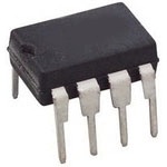
| 供应商器件封装 | 8-PDIP |
| 其它名称 | 24C02LI-G |
| 包装 | 管件 |
| 商标 | ON Semiconductor |
| 存储器类型 | EEPROM |
| 存储容量 | 2 kbit |
| 安装风格 | Through Hole |
| 封装 | Tube |
| 封装/外壳 | 8-DIP(0.300",7.62mm) |
| 封装/箱体 | PDIP-8 |
| 工作温度 | -40°C ~ 85°C |
| 工作电流 | 2 mA |
| 工作电源电压 | 1.8 V , 2.5 V , 3.3 V , 5 V |
| 工厂包装数量 | 50 |
| 接口 | I²C,2 线串口 |
| 接口类型 | I2C |
| 数据保留 | 100 yr |
| 最大工作温度 | + 85 C |
| 最大工作电流 | 2 mA |
| 最大时钟频率 | 0.4 MHz |
| 最小工作温度 | - 40 C |
| 标准包装 | 50 |
| 格式-存储器 | EEPROMs - 串行 |
| 电压-电源 | 1.7 V ~ 5.5 V |
| 电源电压-最大 | 5.5 V |
| 电源电压-最小 | 1.7 V |
| 系列 | CAT24C02 |
| 组织 | 256 x 8 |
| 访问时间 | 900 ns |
| 速度 | 400kHz |


- 商务部:美国ITC正式对集成电路等产品启动337调查
- 曝三星4nm工艺存在良率问题 高通将骁龙8 Gen1或转产台积电
- 太阳诱电将投资9.5亿元在常州建新厂生产MLCC 预计2023年完工
- 英特尔发布欧洲新工厂建设计划 深化IDM 2.0 战略
- 台积电先进制程称霸业界 有大客户加持明年业绩稳了
- 达到5530亿美元!SIA预计今年全球半导体销售额将创下新高
- 英特尔拟将自动驾驶子公司Mobileye上市 估值或超500亿美元
- 三星加码芯片和SET,合并消费电子和移动部门,撤换高东真等 CEO
- 三星电子宣布重大人事变动 还合并消费电子和移动部门
- 海关总署:前11个月进口集成电路产品价值2.52万亿元 增长14.8%


PDF Datasheet 数据手册内容提取
CAT24C02, CAT24C04, CAT24C08, CAT24C16 EEPROM Serial 2/4/8/16(cid:2)Kb I2C Description The CAT24C02/04/08/16 are 2−Kb, 4−Kb, 8−Kb and 16−Kb www.onsemi.com respectively I2C Serial EEPROM devices organized internally as 16/32/64 and 128 pages respectively of 16 bytes each. All devices support both the Standard (100 kHz) as well as Fast (400 kHz) I2C protocol. Data is written by providing a starting address, then loading 1 to 16 UDFN8−EP SOIC−8 WIDE contiguous bytes into a Page Write Buffer, and then writing all data to HU4 SUFFIX X SUFFIX CASE 517AZ non−volatile memory in one internal write cycle. Data is read by CASE 751BE providing a starting address and then shifting out data serially while automatically incrementing the internal address count. External address pins make it possible to address up to eight TSSOP−8 CAT24C02, four CAT24C04, two CAT24C08 and one CAT24C16 TSOT−23 Y SUFFIX TD SUFFIX device on the same bus. CASE 948AL CASE 419AE Features • Supports Standard and Fast I2C Protocol • WLCSP−4** 1.7 V to 5.5 V Supply Voltage Range SOIC−8 C4A SUFFIX • 16−Byte Page Write Buffer W SUFFIX CASE 567DC • CASE 751BD Hardware Write Protection for Entire Memory • Schmitt Triggers and Noise Suppression Filters on I2C Bus Inputs WLCSP−5** WLCSP−4** (SCL and SDA) C5A SUFFIX C4U SUFFIX • Low power CMOS Technology CASE 567DD CASE 567NX • More than 1,000,000 Program/Erase Cycles ** WLCSP are available for the CAT24C04, • 100 Year Data Retention CAT24C08 and CAT24C16 only. • Industrial and Extended Temperature Range For serial EEPROM in the US8 package, please • consult the N24C02 datasheet These Devices are Pb−Free, Halogen Free/BFR Free and are RoHS Compliant ORDERING INFORMATION See detailed ordering and shipping information in the package dimensions section on page 18 of this data sheet. This document contains information on some products that are still under development. ON Semiconductor reserves the right to change or discontinue these products without notice. © Semiconductor Components Industries, LLC, 2016 1 Publication Order Number: October, 2018 − Rev. 34 CAT24C01/D
CAT24C02, CAT24C04, CAT24C08, CAT24C16 PIN CONFIGURATIONS AND MARKING INFORMATION VCC Table 1. PIN FUNCTION Pin Name† Function A0, A1, A2 Device Address Input SCL SDA Serial Data Input/Output SCL Serial Clock Input A2, A1, A0 CAT24Cxx SDA WP Write Protect Input WP VCC Power Supply VSS Ground NC No Connect VSS †The exposed pad for the UDFN packages can be left floating or connected to Ground. Figure 1. Functional Symbol CAT24C__ Pin 1 1 2 Pin 1 1 2 3 16 / 08 / 04 / 02 NC/ NC/NC / A0 1 8 VCC A VCC VSS VCC VSS A NC/ NC/ A1 / A1 2 7 WP SDA B NC/ A2 / A2 / A2 3 6 SCL VSS 4 5 SDA B SCL SDA WP SCL C SOIC (W, X), TSSOP (Y), WLCSP−4*** WLCSP−5*** UDFN−EP (HU4) (Top View) (Top Views) *** WLCSP are available for the CAT24C04, CAT24C08 and CAT24C16 only. TOP MARKING FOR WLCSP (Ball Down) SCL 1 5 WP Pin 1 Pin 1 Pin 1 VSS 2 SDA 3 4 VCC X X X Y M Y W Y M TSOT−23 (TD) (Top View) WLCSP−4 WLCSP−4 WLCSP−5 (C4A) (C4U) X = Specific Device X = Code 4 or R = 24C04 8 or T = 24C08 6 or V = 24C16 Y = Production Year (Last Digit) M = Production Month (1−9, O, N, D) W = Production Week www.onsemi.com 2
CAT24C02, CAT24C04, CAT24C08, CAT24C16 Table 2. ABSOLUTE MAXIMUM RATINGS Parameters Ratings Units Storage Temperature −65 to +150 °C Voltage on any pin with respect to Ground (Note 1) −0.5 to +6.5 V Stresses exceeding those listed in the Maximum Ratings table may damage the device. If any of these limits are exceeded, device functionality should not be assumed, damage may occur and reliability may be affected. 1. During input transitions, voltage undershoot on any pin should not exceed −1 V for more than 20 ns. Voltage overshoot on pins A0, A1, A2 and WP should not exceed VCC + 1 V for more than 20 ns, while voltage on the I2C bus pins, SCL and SDA, should not exceed the absolute maximum ratings, irrespective of VCC. Table 3. RELIABILITY CHARACTERISTICS (Note 2) Symbol Parameter Min Units NEND (Note 3) Endurance 1,000,000 Program / Erase Cycles TDR Data Retention 100 Years 2. These parameters are tested initially and after a design or process change that affects the parameter according to appropriate AEC−Q100 and JEDEC test methods. 3. Page Mode, VCC = 5 V, 25°C. Table 4. D.C. OPERATING CHARACTERISTICS (VCC = 1.8 V to 5.5 V, TA = −40°C to +125°C and VCC = 1.7 V to 5.5 V, TA = −40°C to +85°C, unless otherwise specified.) Symbol Parameter Test Conditions Min Max Units ICCR Read Current Read, fSCL = 400 kHz 1 mA ICCW Write Current Write, fSCL = 400 kHz 2 mA ISB Standby Current All I/O Pins at GND or VCC TA = −40°C to +85°C 1 (cid:2)A VCC ≤ 3.3 V TA = −40°C to +85°C 3 VCC > 3.3 V TA = −40°C to +125°C 5 IL I/O Pin Leakage Pin at GND or VCC 2 (cid:2)A VIL Input Low Voltage −0.5 0.3 x VCC V VIH Input High Voltage A0, A1, A2 and WP 0.7 x VCC VCC + 0.5 V SCL and SDA 0.7 x VCC 5.5 VOL Output Low VCC > 2.5 V, IOL = 3 mA 0.4 Voltage VCC < 2.5 V, IOL = 1 mA 0.2 Product parametric performance is indicated in the Electrical Characteristics for the listed test conditions, unless otherwise noted. Product performance may not be indicated by the Electrical Characteristics if operated under different conditions. www.onsemi.com 3
CAT24C02, CAT24C04, CAT24C08, CAT24C16 Table 5. PIN IMPEDANCE CHARACTERISTICS (VCC = 1.8 V to 5.5 V, TA = −40°C to +125°C and VCC = 1.7 V to 5.5 V, TA = −40°C to +85°C, unless otherwise specified.) Symbol Parameter Conditions Max Units CIN (Note 4) SDA Pin Capacitance VIN = 0 V, f = 1.0 MHz, VCC = 5.0 V 8 pF Other Pins 6 pF IWP (Note 5) WP Input Current VIN < VIH, VCC = 5.5 V 130 (cid:2)A VIN < VIH, VCC = 3.3 V 120 VIN < VIH, VCC = 1.7 V 80 VIN > VIH 2 IA (Note 5) Address Input Current VIN < VIH, VCC = 5.5 V 50 (cid:2)A (A0, A1, A2) Product Rev H: CAT24C02 VIN < VIH, VCC = 3.3 V 35 Product Rev K: CAT24C04, CAT24C08, CAT24C16 VIN < VIH, VCC = 1.7 V 25 VIN > VIH 2 4. These parameters are tested initially and after a design or process change that affects the parameter according to appropriate AEC−Q100 and JEDEC test methods. 5. When not driven, the WP, A0, A1 and A2 pins are pulled down to GND internally. For improved noise immunity, the internal pull−down is relatively strong; therefore the external driver must be able to supply the pull−down current when attempting to drive the input HIGH. To conserve power, as the input level exceeds the trip point of the CMOS input buffer (~ 0.5 x VCC), the strong pull−down reverts to a weak current source. Table 6. A.C. CHARACTERISTICS (Note 6) (VCC = 1.8 V to 5.5 V, TA = −40°C to +125°C and VCC = 1.7 V to 5.5 V, TA = −40°C to +85°C, unless otherwise specified.) Standard Fast Symbol Parameter Min Max Min Max Units FSCL Clock Frequency 100 400 kHz tHD:STA START Condition Hold Time 4 0.6 (cid:2)s tLOW Low Period of SCL Clock 4.7 1.3 (cid:2)s tHIGH High Period of SCL Clock 4 0.6 (cid:2)s tSU:STA START Condition Setup Time 4.7 0.6 (cid:2)s tHD:DAT Data In Hold Time 0 0 (cid:2)s tSU:DAT Data In Setup Time 250 100 ns tR SDA and SCL Rise Time 1000 300 ns tF (Note 6) SDA and SCL Fall Time 300 300 ns tSU:STO STOP Condition Setup Time 4 0.6 (cid:2)s tBUF Bus Free Time Between STOP and START 4.7 1.3 (cid:2)s tAA SCL Low to Data Out Valid 3.5 0.9 (cid:2)s tDH Data Out Hold Time 100 100 ns Ti (Note 6) Noise Pulse Filtered at SCL and SDA Inputs 100 100 ns tSU:WP WP Setup Time 0 0 (cid:2)s tHD:WP WP Hold Time 2.5 2.5 (cid:2)s tWR Write Cycle Time 5 5 ms tPU (Notes 7, 8) Power−up to Ready Mode 1 1 ms 6. Test conditions according to “AC Test Conditions” table. 7. Tested initially and after a design or process change that affects this parameter. 8. tPU is the delay between the time VCC is stable and the device is ready to accept commands. www.onsemi.com 4
CAT24C02, CAT24C04, CAT24C08, CAT24C16 Table 7. A.C. TEST CONDITIONS Input Drive Levels 0.2 x VCC to 0.8 x VCC Input Rise and Fall Time (cid:2) 50 ns Input Reference Levels 0.3 x VCC, 0.7 x VCC Output Reference Level 0.5 x VCC Output Test Load Current Source IOL = 3 mA (VCC (cid:3) 2.5 V); IOL = 1 mA (VCC < 2.5 V); CL = 100 pF Power−On Reset (POR) During data transfer, the SDA line must remain stable Each CAT24Cxx* incorporates Power−On Reset (POR) while the SCL line is high. An SDA transition while SCL is circuitry which protects the internal logic against powering high will be interpreted as a START or STOP condition up in the wrong state. (Figure 2). The START condition precedes all commands. It A CAT24Cxx device will power up into Standby mode consists of a HIGH to LOW transition on SDA while SCL after V exceeds the POR trigger level and will power is HIGH. The START acts as a ‘wake−up’ call to all CC down into Reset mode when V drops below the POR receivers. Absent a START, a Slave will not respond to CC trigger level. This bi−directional POR feature protects the commands. The STOP condition completes all commands. device against ‘brown−out’ failure following a temporary It consists of a LOW to HIGH transition on SDA while SCL loss of power. is HIGH. *For common features, the CAT24C02/04/08/16 will be NOTE: The I/O pins of CAT24Cxx do not obstruct the SCL referred to as CAT24Cxx. and SDA lines if the VCC supply is switched off. During power−up, the SCL and SDA pins (connected with pull−up Pin Description resistors to VCC) will follow the VCC monotonically from SCL: The Serial Clock input pin accepts the Serial Clock VSS (0 V) to nominal VCC value, regardless of pull−up generated by the Master. resistor value. The delta between the VCC and the SDA: The Serial Data I/O pin receives input data and instantaneous voltage levels during power ramping will be determined by the relation between bus time constant transmits data stored in EEPROM. In transmit mode, this pin (determined by pull−up resistance and bus capacitance) and is open drain. Data is acquired on the positive edge, and is actual VCC ramp rate. delivered on the negative edge of SCL. A0, A1 and A2: The Address inputs set the device address Device Addressing when cascading multiple devices. When not driven, these The Master initiates data transfer by creating a START pins are pulled LOW internally. condition on the bus. The Master then broadcasts an 8−bit WP: The Write Protect input pin inhibits all write serial Slave address. For normal Read/Write operations, the operations, when pulled HIGH. When not driven, this pin is first 4 bits of the Slave address are fixed at 1010 (Ah). The pulled LOW internally. next 3 bits are used as programmable address bits when cascading multiple devices and/or as internal address bits. Functional Description The last bit of the slave address, R/W, specifies whether a The CAT24Cxx supports the Inter−Integrated Circuit Read (1) or Write (0) operation is to be performed. The 3 (I2C) Bus data transmission protocol, which defines a device address space extension bits are assigned as illustrated in that sends data to the bus as a transmitter and a device Figure 3. A , A and A must match the state of the external 2 1 0 receiving data as a receiver. Data flow is controlled by a address pins, and a , a and a are internal address bits. 10 9 8 Master device, which generates the serial clock and all START and STOP conditions. The CAT24Cxx acts as a Acknowledge Slave device. Master and Slave alternate as either After processing the Slave address, the Slave responds transmitter or receiver. with an acknowledge (ACK) by pulling down the SDA line during the 9th clock cycle (Figure 4). The Slave will also I2C Bus Protocol acknowledge the address byte and every data byte presented The I2C bus consists of two ‘wires’, SCL and SDA. The in Write mode. In Read mode the Slave shifts out a data byte, two wires are connected to the VCC supply via pull−up and then releases the SDA line during the 9th clock cycle. As resistors. Master and Slave devices connect to the 2−wire long as the Master acknowledges the data, the Slave will bus via their respective SCL and SDA pins. The transmitting continue transmitting. The Master terminates the session by device pulls down the SDA line to ‘transmit’ a ‘0’ and not acknowledging the last data byte (NoACK) and by releases it to ‘transmit’ a ‘1’. issuing a STOP condition. Bus timing is illustrated in Data transfer may be initiated only when the bus is not Figure 5. busy (see AC Characteristics). www.onsemi.com 5
CAT24C02, CAT24C04, CAT24C08, CAT24C16 SCL SDA START STOP CONDITION CONDITION Figure 2. Start/Stop Timing 1 0 1 0 A2 A1 A0 R/W CAT24C02 1 0 1 0 A2 A1 a8 R/W CAT24C04 1 0 1 0 A2 a9 a8 R/W CAT24C08 1 0 1 0 a10 a9 a8 R/W CAT24C16 Figure 3. Slave Address Bits BUS RELEASE DELAY (TRANSMITTER) BUS RELEASE DELAY (RECEIVER) SCL FROM 1 8 9 MASTER DATA OUTPUT FROM TRANSMITTER DATA OUTPUT FROM RECEIVER ACK SETUP ((cid:3) tSU:DAT) START ACK DELAY ((cid:2) tAA) Figure 4. Acknowledge Timing tF tHIGH tR tLOW tLOW SCL tSU:STA tHD:DAT tHD:SDA tSU:DAT tSU:STO SDA IN tAA tDH tBUF SDA OUT Figure 5. Bus Timing www.onsemi.com 6
CAT24C02, CAT24C04, CAT24C08, CAT24C16 WRITE OPERATIONS Byte Write sixteen bytes are received and the STOP condition has been In Byte Write mode, the Master sends the START sent by the Master, the internal Write cycle begins. At this condition and the Slave address with the R/W bit set to zero point all received data is written to the CAT24Cxx in a single to the Slave. After the Slave generates an acknowledge, the write cycle. Master sends the byte address that is to be written into the address pointer of the CAT24Cxx. After receiving another Acknowledge Polling acknowledge from the Slave, the Master transmits the data The acknowledge (ACK) polling routine can be used to byte to be written into the addressed memory location. The take advantage of the typical write cycle time. Once the stop CAT24Cxx device will acknowledge the data byte and the condition is issued to indicate the end of the host’s write operation, the CAT24Cxx initiates the internal write cycle. Master generates the STOP condition, at which time the The ACK polling can be initiated immediately. This device begins its internal Write cycle to nonvolatile memory involves issuing the start condition followed by the slave (Figure 6). While this internal cycle is in progress (t ), the WR address for a write operation. If the CAT24Cxx is still busy SDA output will be tri−stated and the CAT24Cxx will not with the write operation, NoACK will be returned. If the respond to any request from the Master device (Figure 7). CAT24Cxx has completed the internal write operation, an Page Write ACK will be returned and the host can then proceed with the The CAT24Cxx writes up to 16 bytes of data in a single next read or write operation. write cycle, using the Page Write operation (Figure 8). The Page Write operation is initiated in the same manner as the Hardware Write Protection With the WP pin held HIGH, the entire memory is Byte Write operation, however instead of terminating after the data byte is transmitted, the Master is allowed to send up protected against Write operations. If the WP pin is left to fifteen additional bytes. After each byte has been floating or is grounded, it has no impact on the operation of the CAT24Cxx. The state of the WP pin is strobed on the last transmitted the CAT24Cxx will respond with an falling edge of SCL immediately preceding the first data acknowledge and internally increments the four low order byte (Figure 9). If the WP pin is HIGH during the strobe address bits. The high order bits that define the page address interval, the CAT24Cxx will not acknowledge the data byte remain unchanged. If the Master transmits more than sixteen and the Write request will be rejected. bytes prior to sending the STOP condition, the address counter ‘wraps around’ to the beginning of page and Delivery State previously transmitted data will be overwritten. Once all The CAT24Cxx is shipped erased, i.e., all bytes are FFh. BUS ACTIVITY: S T S ADDRESS DATA A SLAVE BYTE BYTE T MASTER R ADDRESS O T a7− a0 d7− d0 P S P A A A SLAVE C C C K K K Figure 6. Byte Write Sequence www.onsemi.com 7
CAT24C02, CAT24C04, CAT24C08, CAT24C16 SCL SDA 8th Bit ACK Byte n tWR STOP START ADDRESS CONDITION CONDITION Figure 7. Write Cycle Timing BUS ACTIVITY: S T DATA DATA DATA S A SLAVE ADDRESS BYTE BYTE BYTE T MASTER R ADDRESS BYTE n n+1 n+P O T P S P A A A A A SLAVE C C C C C K K K K K n = 1 P (cid:2) 15 Figure 8. Page Write Sequence ADDRESS DATA BYTE BYTE 1 8 9 1 8 SCL SDA a7 a0 d7 d0 tSU:WP WP tHD:WP Figure 9. WP Timing www.onsemi.com 8
CAT24C02, CAT24C04, CAT24C08, CAT24C16 READ OPERATIONS Immediate Read address of the location it wishes to read. After the Upon receiving a Slave address with the R/W bit set to ‘1’, CAT24Cxx acknowledges the byte address, the Master the CAT24Cxx will interpret this as a request for data device resends the START condition and the slave address, residing at the current byte address in memory. The this time with the R/W bit set to one. The CAT24Cxx then CAT24Cxx will acknowledge the Slave address, will responds with its acknowledge and sends the requested data immediately shift out the data residing at the current address, byte. The Master device does not acknowledge the data and will then wait for the Master to respond. If the Master (NoACK) but will generate a STOP condition (Figure 11). does not acknowledge the data (NoACK) and then follows up with a STOP condition (Figure 10), the CAT24Cxx Sequential Read If during a Read session, the Master acknowledges the 1st returns to Standby mode. data byte, then the CAT24Cxx will continue transmitting Selective Read data residing at subsequent locations until the Master Selective Read operations allow the Master device to responds with a NoACK, followed by a STOP (Figure 12). select at random any memory location for a read operation. In contrast to Page Write, during Sequential Read the The Master device first performs a ‘dummy’ write operation address count will automatically increment to and then by sending the START condition, slave address and byte wrap−around at end of memory (rather than end of page). N BUS ACTIVITY: S O T S A SLAVE A T MASTER R ADDRESS CO T KP S P A SLAVE C DATA K BYTE SCL 8 9 SDA 8th Bit DATA OUT NO ACK STOP Figure 10. Immediate Read Sequence and Timing N BUS ACTIVITY: S S O T T S A SLAVE ADDRESS A SLAVE AT MASTER R ADDRESS BYTE R ADDRESS CO T T KP S S P A A A SLAVE C C C DATA BYTE K K K Figure 11. Selective Read Sequence N BUS ACTIVITY: O S SLAVE A A A A T MASTER ADDRESS C C C CO K K K KP P A SLAVE C DATA DATA DATA DATA K BYTE BYTE BYTE BYTE n n+1 n+2 n+x Figure 12. Sequential Read Sequence www.onsemi.com 9
CAT24C02, CAT24C04, CAT24C08, CAT24C16 PACKAGE DIMENSIONS SOIC−8, 208 mils CASE 751BE−01 ISSUE O SYMBOL MIN NOM MAX A 2.03 A1 0.05 0.25 b 0.36 0.48 c 0.19 0.25 E1 E D 5.13 5.33 E 7.75 8.26 E1 5.13 5.38 e 1.27 BSC L 0.51 0.76 θ 0º 8º PIN#1 IDENTIFICATION TOP VIEW D A (cid:3) e b L c A1 SIDE VIEW END VIEW Notes: (1) All dimensions are in millimeters. Angles in degrees. (2) Complies with EIAJ EDR-7320. www.onsemi.com 10
CAT24C02, CAT24C04, CAT24C08, CAT24C16 PACKAGE DIMENSIONS SOIC 8, 150 mils CASE 751BD ISSUE O SYMBOL MIN NOM MAX A 1.35 1.75 A1 0.10 0.25 b 0.33 0.51 c 0.19 0.25 E1 E D 4.80 5.00 E 5.80 6.20 E1 3.80 4.00 e 1.27 BSC h 0.25 0.50 L 0.40 1.27 PIN # 1 IDENTIFICATION θ 0º 8º TOP VIEW D h A1 θ A c e b L SIDE VIEW END VIEW Notes: (1) All dimensions are in millimeters. Angles in degrees. (2) Complies with JEDEC MS-012. www.onsemi.com 11
CAT24C02, CAT24C04, CAT24C08, CAT24C16 PACKAGE DIMENSIONS TSSOP8, 4.4x3 CASE 948AL b ISSUE O SYMBOL MIN NOM MAX A 1.20 A1 0.05 0.15 A2 0.80 0.90 1.05 b 0.19 0.30 E1 E c 0.09 0.20 D 2.90 3.00 3.10 E 6.30 6.40 6.50 E1 4.30 4.40 4.50 e 0.65 BSC L 1.00 REF L1 0.50 0.60 0.75 θ 0º 8º e TOP VIEW D A2 A (cid:3)1 c A1 L1 L SIDE VIEW END VIEW Notes: (1) All dimensions are in millimeters. Angles in degrees. (2) Complies with JEDEC MO-153. www.onsemi.com 12
CAT24C02, CAT24C04, CAT24C08, CAT24C16 PACKAGE DIMENSIONS TSOT−23, 5 LEAD CASE 419AE ISSUE O SYMBOL MIN NOM MAX D A 1.00 e A1 0.01 0.05 0.10 A2 0.80 0.87 0.90 b 0.30 0.45 c 0.12 0.15 0.20 D 2.90 BSC E1 E E 2.80 BSC E1 1.60 BSC e 0.95 TYP L 0.30 0.40 0.50 L1 0.60 REF L2 0.25 BSC θ 0º 8º TOP VIEW A2 A (cid:3) L b A1 c L2 L1 SIDE VIEW END VIEW Notes: (1) All dimensions are in millimeters. Angles in degrees. (2) Complies with JEDEC MO-193. www.onsemi.com 13
CAT24C02, CAT24C04, CAT24C08, CAT24C16 PACKAGE DIMENSIONS UDFN8, 2x3 EXTENDED PAD CASE 517AZ ISSUE O D A b e L DAP SIZE 1.8 x 1.8 E E2 PIN #1 IDENTIFICATION A1 PIN #1 INDEX AREA D2 TOP VIEW SIDE VIEW BOTTOM VIEW SYMBOL MIN NOM MAX A 0.45 0.50 0.55 A1 0.00 0.02 0.05 A3 0.127 REF b 0.20 0.25 0.30 0.065 REF DETAIL A A3 A D 1.95 2.00 2.05 FRONT VIEW D2 1.35 1.40 1.45 E 2.95 3.00 3.05 E2 1.25 1.30 1.35 e 0.50 REF L 0.25 0.30 0.35 0.065 REF A3 0.0 - 0.05 Notes: Copper Exposed (1) (cid:3)All dimensions are in millimeters. (2) Refer JEDEC MO-236/MO-252. DETAIL A www.onsemi.com 14
CAT24C02, CAT24C04, CAT24C08, CAT24C16 PACKAGE DIMENSIONS WLCSP4, 0.84x0.86 CASE 567NX ISSUE A E A B NOTES: 1. DIMENSIONING AND TOLERANCING PER ASME PIN A1 ÈÈ Y14.5M, 1994. REFERENCE 2. CONTROLLING DIMENSION: MILLIMETERS. 3. DATUM C, THE SEATING PLANE, IS DEFINED BY ÈÈ D THE SPHERICAL CROWNS OF THE CONTACT BALLS. A3 4. COPLANARITY APPLIES TO SPHERICAL CROWNS OF THE CONTACT BALLS. TOP VIEW OPTIONAL A2 5. DIMENSION b IS MEASURED AT THE MAXIMUM BACKSIDE COAT CONTACT BALL DIAMETER PARALLEL TO DATUM C. MILLIMETERS DETAIL A A DIM MIN NOM MAX 0.05 C DETAIL A A −−− −−− 0.30 A1 0.08 0.10 0.12 A2 0.15 REF A3 0.025 REF 0.05 C b 0.16 0.18 0.20 NOTE 4 A1 C SPELAATNIENG DE 00..8824 00..8846 00..8868 SIDE VIEW NOTE 3 e 0.40 BSC RECOMMENDED e 4X b e SOLDERING FOOTPRINT* 0.05 C A B A1 PACKAGE 0.03 C NOTE 5 B OUTLINE A 1 2 BOTTOM VIEW 0.40 4X 0.18 PITCH 0.40 PITCH DIMENSIONS: MILLIMETERS *For additional information on our Pb−Free strategy and soldering details, please download the ON Semiconductor Soldering and Mounting Techniques Reference Manual, SOLDERRM/D. www.onsemi.com 15
CAT24C02, CAT24C04, CAT24C08, CAT24C16 PACKAGE DIMENSIONS WLCSP4, 0.84x0.86 CASE 567DC ISSUE D E A B NOTES: 1. DIMENSIONING AND TOLERANCING PER ASME PIN A1 ÈÈ Y14.5M, 1994. REFERENCE 2. CONTROLLING DIMENSION: MILLIMETERS. ÈÈ 3. DATUM C, THE SEATING PLANE, IS DEFINED BY D THE SPHERICAL CROWNS OF THE CONTACT 2X 0.10 C BALLS. 4. COPLANARITY APPLIES TO SPHERICAL CROWNS OF THE CONTACT BALLS. 2X 0.10 C TOP VIEW A2 5. DCIOMNETNASCITO NB AbL ILS DMIAEMASEUTERRE DP AART ATLHLEE LM TAOX IDMAUTMUM C. * Die Coat A3* A (Optional) MILLIMETERS DIM MIN MAX A 0.28 0.38 A2 DETAIL A A DETAIL A AA12 0.00.823 RE0F.12 0.10 C A3* 0.025 REF b 0.16 0.20 D 0.84 BSC 0.05 C E 0.86 BSC e 0.40 BSC NOTE 4 A1 C SPELAATNIENG * Die Coat (Optional) SIDE VIEW NOTE 3 RECOMMENDED e SOLDERING FOOTPRINT* 4X b e A1 PACKAGE 0.10 M C A B OUTLINE B NOTE 5 A 1 2 BOTTOM VIEW 0.40 4X0.18 PITCH 0.40 PITCH DIMENSIONS: MILLIMETERS *For additional information on our Pb−Free strategy and soldering details, please download the ON Semiconductor Soldering and Mounting Techniques Reference Manual, SOLDERRM/D. www.onsemi.com 16
CAT24C02, CAT24C04, CAT24C08, CAT24C16 PACKAGE DIMENSIONS WLCSP5, 0.86x0.84 CASE 567DD ISSUE C E A B NOTES: ÈÈ 1. DIMENSIONING AND TOLERANCING PER ASME PIN A1 Y14.5M, 1994. REFERENCE 2. CONTROLLING DIMENSION: MILLIMETERS. ÈÈ 3. DATUM C, THE SEATING PLANE, IS DEFINED BY THE D SPHERICAL CROWNS OF THE CONTACT BALLS. 2X 0.10 C 4. COPLANARITY APPLIES TO SPHERICAL CROWNS OF THE CONTACT BALLS. 5. DIMENSION b IS MEASURED AT THE MAXIMUM CON- 2X 0.10 C TACT BALL DIAMETER PARALLEL TO DATUM C. TOP VIEW MILLIMETERS DIM MIN MAX A A 0.29 0.39 A2 A1 0.10 0.14 0.10 C A2 0.23 REF b 0.14 0.18 D 0.86 BSC 5X 0.05 C E 0.84 BSC NOTE 3 A1 C SPELAATNIENG ee1 00..3502 BBSSCC SIDE VIEW RECOMMENDED e SOLDERING FOOTPRINT* 5X b e1 A1 PACKAGE 0.10 M C A B OUTLINE C NOTE 4 B A PIN A1 123 REFERENCE 5X BOTTOM VIEW 0.52 0.16 PITCH 0.30 PITCH DIMENSIONS: MILLIMETERS *For additional information on our Pb−Free strategy and soldering details, please download the ON Semiconductor Soldering and Mounting Techniques Reference Manual, SOLDERRM/D. www.onsemi.com 17
CAT24C02, CAT24C04, CAT24C08, CAT24C16 Ordering Information CAT24C02 Ordering Information (Notes 10, 11) Specific Package Temperature Lead Device Order Number Device Marking Type Range (Note 9) Finish Shipping CAT24C02TDI−GT3A C1 TSOT−23−5 Industrial NiPdAu Tape & Reel, 3,000 Units / Reel CAT24C04 Ordering Information Specific Package Temperature Lead Device Order Number Device Marking Type Range (Note 9) Finish Shipping CAT24C04WI−GT3 24C04K SOIC−8 Industrial NiPdAu Tape & Reel, 3,000 Units / Reel CAT24C04XI−T2 (Note 17) TBD SOIC−8 Industrial Matte−Tin Tape & Reel, 2,000 Units / Reel CAT24C04YI−GT3 C04K TSSOP−8 Industrial NiPdAu Tape & Reel, 3,000 Units / Reel CAT24C04C4UTR R WLCSP−4 Industrial N/A (Notes 12 and 13) CAT24C04C4ATR 4 WLCSP−4 Industrial N/A Tape & Reel, 5,000 Units / Reel CAT24C04C5ATR 4 WLCSP−5 Industrial N/A Tape & Reel, 5,000 Units / Reel CAT24C04TDI−GT3 C2 TSOT−23−5 Industrial NiPdAu Tape & Reel, 3,000 Units / Reel CAT24C04HU4I−GT3 C2U UDFN8−EP Industrial NiPdAu Tape & Reel, 3,000 Units / Reel CAT24C08 Ordering Information Specific Package Temperature Lead Device Order Number Device Marking Type Range (Note 9) Finish Shipping CAT24C08WI−GT3 24C08K SOIC−8 Industrial NiPdAu Tape & Reel, 3,000 Units / Reel CAT24C08XI−T2 (Note 17) TBD SOIC−8 Industrial Matte−Tin Tape & Reel, 2,000 Units / Reel CAT24C08YI−GT3 C08K TSSOP−8 Industrial NiPdAu Tape & Reel, 3,000 Units / Reel CAT24C08C4UTR T WLCSP−4 Industrial N/A (Notes 12 and 13) CAT24C08C4ATR 8 WLCSP−4 Industrial N/A Tape & Reel, 5,000 Units / Reel CAT24C08C4CTR** 8 WLCSP−4 Industrial N/A Tape & Reel, 5,000 Units / Reel CAT24C08C5ATR 8 WLCSP−5 Industrial N/A Tape & Reel, 5,000 Units / Reel CAT24C08TDI−GT3 C3 TSOT−23−5 Industrial NiPdAu Tape & Reel, 3,000 Units / Reel CAT24C08HU4I−GT3 C3U UDFN8−EP Industrial NiPdAu Tape & Reel, 3,000 Units / Reel CAT24C16 Ordering Information Specific Package Temperature Lead Device Order Number Device Marking Type Range (Note 9) Finish Shipping CAT24C16WI−GT3 24C16K SOIC−8 Industrial NiPdAu Tape & Reel, 3,000 Units / Reel CAT24C16XI−T2 (Note 17) TBD SOIC−8 Industrial Matte−Tin Tape & Reel, 2,000 Units / Reel CAT24C16YI−GT3 C16K TSSOP−8 Industrial NiPdAu Tape & Reel, 3,000 Units / Reel CAT24C16C4UTR 6 WLCSP−4 Industrial N/A (Notes 12 and 13) CAT24C16C4ATR 6 WLCSP−4 Industrial N/A Tape & Reel, 5,000 Units / Reel CAT24C16C5ATR 6 WLCSP−5 Industrial N/A Tape & Reel, 5,000 Units / Reel CAT24C16TDI−GT3 C4 TSOT−23−5 Industrial NiPdAu Tape & Reel, 3,000 Units / Reel CAT24C16HU4I−GT3 C4U UDFN8−EP Industrial NiPdAu Tape & Reel, 3,000 Units / Reel CAT24C16HU4E−GT3 (Note 17) C4E UDFN8−EP Extended NiPdAu Tape & Reel, 3,000 Units / Reel 9. Industrial temperature range is −40°C to +85°C and Extended temperature range is −40°C to +125°C. 10.Part numbers ending with “A” for the CAT24C02 are for Gresham (Product Rev H) only die. 11.The CAT24C02 “non−A” Device Order Numbers use Gresham die (Rev H) for date codes, starting August 1st, 2012. Therefore the Specific Device Marking for these OPNs reflect Rev H die. 12.Contact local sales office for availability. 13.CAUTION: The EEPROM devices delivered in WLCSP must never be exposed to ultraviolet light. When exposed to ultraviolet light the EEPROM cells lose their stored data. 14.All packages are RoHS−compliant (Lead−free, Halogen−free). 15.For information on tape and reel specifications, including part orientation and tape sizes, please refer to our Tape and Reel Packaging Specifications Brochure, BRD8011/D. 16.For detailed information and a breakdown of device nomenclature and numbering systems, please see the ON Semiconductor Device Nomenclature document, TND310/D, available at www.onsemi.com 17.In Development ** CAT24C08C4CTR is a backside coated version. Contact factory for other densities. www.onsemi.com 18
CAT24C02, CAT24C04, CAT24C08, CAT24C16 ON Semiconductor and are trademarks of Semiconductor Components Industries, LLC dba ON Semiconductor or its subsidiaries in the United States and/or other countries. ON Semiconductor owns the rights to a number of patents, trademarks, copyrights, trade secrets, and other intellectual property. A listing of ON Semiconductor’s product/patent coverage may be accessed at www.onsemi.com/site/pdf/Patent−Marking.pdf. ON Semiconductor reserves the right to make changes without further notice to any products herein. ON Semiconductor makes no warranty, representation or guarantee regarding the suitability of its products for any particular purpose, nor does ON Semiconductor assume any liability arising out of the application or use of any product or circuit, and specifically disclaims any and all liability, including without limitation special, consequential or incidental damages. Buyer is responsible for its products and applications using ON Semiconductor products, including compliance with all laws, regulations and safety requirements or standards, regardless of any support or applications information provided by ON Semiconductor. “Typical” parameters which may be provided in ON Semiconductor data sheets and/or specifications can and do vary in different applications and actual performance may vary over time. All operating parameters, including “Typicals” must be validated for each customer application by customer’s technical experts. ON Semiconductor does not convey any license under its patent rights nor the rights of others. ON Semiconductor products are not designed, intended, or authorized for use as a critical component in life support systems or any FDA Class 3 medical devices or medical devices with a same or similar classification in a foreign jurisdiction or any devices intended for implantation in the human body. Should Buyer purchase or use ON Semiconductor products for any such unintended or unauthorized application, Buyer shall indemnify and hold ON Semiconductor and its officers, employees, subsidiaries, affiliates, and distributors harmless against all claims, costs, damages, and expenses, and reasonable attorney fees arising out of, directly or indirectly, any claim of personal injury or death associated with such unintended or unauthorized use, even if such claim alleges that ON Semiconductor was negligent regarding the design or manufacture of the part. ON Semiconductor is an Equal Opportunity/Affirmative Action Employer. This literature is subject to all applicable copyright laws and is not for resale in any manner. PUBLICATION ORDERING INFORMATION LITERATURE FULFILLMENT: N. American Technical Support: 800−282−9855 Toll Free ON Semiconductor Website: www.onsemi.com Literature Distribution Center for ON Semiconductor USA/Canada 19521 E. 32nd Pkwy, Aurora, Colorado 80011 USA Europe, Middle East and Africa Technical Support: Order Literature: http://www.onsemi.com/orderlit Phone: 303−675−2175 or 800−344−3860 Toll Free USA/Canada Phone: 421 33 790 2910 Fax: 303−675−2176 or 800−344−3867 Toll Free USA/Canada For additional information, please contact your local Email: orderlit@onsemi.com Sales Representative ◊ www.onsemi.com CAT24C01/D 19