
 Datasheet下载
- 型号: M25P32-VMW6G
- 制造商: Micron Technology Inc
- 库位|库存: xxxx|xxxx
- 要求:
| 数量阶梯 | 香港交货 | 国内含税 |
| +xxxx | $xxxx | ¥xxxx |
查看当月历史价格
查看今年历史价格
M25P32-VMW6G产品简介:
ICGOO电子元器件商城为您提供M25P32-VMW6G由Micron Technology Inc设计生产,在icgoo商城现货销售,并且可以通过原厂、代理商等渠道进行代购。 M25P32-VMW6G价格参考。Micron Technology IncM25P32-VMW6G封装/规格:存储器, FLASH - NOR 存储器 IC 32Mb (4M x 8) SPI 75MHz 8-SO。您可以下载M25P32-VMW6G参考资料、Datasheet数据手册功能说明书,资料中有M25P32-VMW6G 详细功能的应用电路图电压和使用方法及教程。
Micron Technology Inc.生产的M25P32-VMW6G是一款串行闪存存储器,广泛应用于多种嵌入式系统和消费电子设备中。这款器件的主要应用场景包括:

1. 嵌入式系统:M25P32-VMW6G常用于微控制器、单片机(MCU)和其他嵌入式处理器的外部存储扩展。它提供非易失性存储,用于存放启动代码、固件、配置参数等关键数据。其高速读写性能确保了系统的快速启动和高效运行。

2. 物联网(IoT)设备:在智能家居、智能穿戴设备、传感器节点等IoT应用中,M25P32-VMW6G可以作为主控芯片的外部存储,存储设备的固件和用户设置。其低功耗特性有助于延长电池寿命,而高可靠性则保证了数据的安全性和完整性。

3. 工业自动化:在工业控制系统、PLC(可编程逻辑控制器)、HMI(人机界面)等设备中,M25P32-VMW6G可用于存储程序代码、配置文件和历史数据。其宽工作温度范围(-40°C至+85°C)使其适用于各种恶劣环境,确保工业设备的稳定运行。

4. 消费电子产品:如数字相机、打印机、便携式媒体播放器等设备中,M25P32-VMW6G可以存储设备的固件和用户设置,确保设备的功能性和个性化体验。其小尺寸封装(如SOP-8)使得它非常适合于对空间要求严格的消费类应用。

5. 通信设备:在网络路由器、交换机、调制解调器等通信设备中,M25P32-VMW6G可以存储引导加载程序、操作系统映像和网络配置参数。其高速读取性能有助于加快设备的初始化过程,提高网络设备的响应速度。

总之,M25P32-VMW6G凭借其高性能、低功耗、高可靠性和紧凑的封装设计,成为众多嵌入式系统和消费电子设备的理想选择,特别适用于需要稳定、快速和非易失性存储的应用场景。
| 参数 | 数值 |
| 产品目录 | 集成电路 (IC) |
| 描述 | IC FLASH 32MBIT 75MHZ 8SO |
| 产品分类 | |
| 品牌 | Micron Technology Inc |
| 数据手册 | |
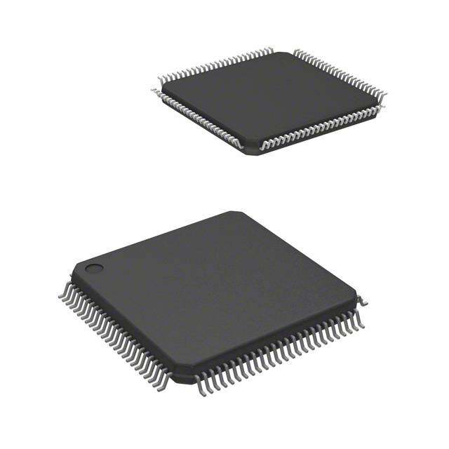
| 产品图片 |
|
| 产品型号 | M25P32-VMW6G |
| rohs | 无铅 / 符合限制有害物质指令(RoHS)规范要求 |
| 产品系列 | - |
| 产品目录页面 | |
| 供应商器件封装 | 8-SO W |
| 其它名称 | M25P32VMW6G |
| 包装 | 管件 |
| 存储器类型 | FLASH - NOR |
| 存储容量 | 32M(4M x 8) |
| 封装/外壳 | 8-SOIC(0.209",5.30mm 宽) |
| 工作温度 | -40°C ~ 85°C |
| 接口 | SPI 串行 |
| 标准包装 | 1,800 |
| 格式-存储器 | 闪存 |
| 电压-电源 | 2.7 V ~ 3.6 V |
| 速度 | 75MHz |


_renders/IS42S32800D-6BLI.jpg)

- 商务部:美国ITC正式对集成电路等产品启动337调查
- 曝三星4nm工艺存在良率问题 高通将骁龙8 Gen1或转产台积电
- 太阳诱电将投资9.5亿元在常州建新厂生产MLCC 预计2023年完工
- 英特尔发布欧洲新工厂建设计划 深化IDM 2.0 战略
- 台积电先进制程称霸业界 有大客户加持明年业绩稳了
- 达到5530亿美元!SIA预计今年全球半导体销售额将创下新高
- 英特尔拟将自动驾驶子公司Mobileye上市 估值或超500亿美元
- 三星加码芯片和SET,合并消费电子和移动部门,撤换高东真等 CEO
- 三星电子宣布重大人事变动 还合并消费电子和移动部门
- 海关总署:前11个月进口集成电路产品价值2.52万亿元 增长14.8%


PDF Datasheet 数据手册内容提取
M25P32 Serial Flash Embedded Memory Features M25P32 32Mb 3V NOR Serial Flash Embedded Memory Features • Electronic signature – JEDEC-standard 2-byte signature (2016h) • SPI bus-compatible serial interface – Unique ID code (UID) and 16 bytes of common • 32Mb Flash memory Flash interface (CFI) data • 75 MHz clock frequency (maximum) – RES command, one-byte signature (15h) for • 2.7V to 3.6V single supply voltage backward-compatibility • VPP = 9V for FAST PROGRAM/ERASE mode (option- • More than 100,000 write cycles per sector al) • More than 20 years of data retention • Page program (up to 256 bytes) in 0.64ms (TYP) • Automotive-grade parts available • Erase capability • Packages (RoHS-compliant) – Sector erase: 512Kb in 0.6s (TYP) – SO8W (MW) 208 mils – Bulk erase: 23 s (TYP); 17s (TYP) with VPP = 9V – SO16 (MF) 300 mils • Write protection – VFQFPN8 (MP) MLP8 6mm x 5mm – Hardware write protection: protected area size – VFDFPN8 (MP) MLP8 8mm x 6mm defined by nonvolatile bits BP0, BP1, BP2 • Deep power-down: 1µA (TYP) 09005aef84566541 1 Micron Technology, Inc. reserves the right to change products or specifications without notice. m25p32.pdf - Rev. R 06/18 EN © 2013 Micron Technology, Inc. All rights reserved. Products and specifications discussed herein are subject to change by Micron without notice.
M25P32 Serial Flash Embedded Memory Features Contents Important Notes and Warnings ......................................................................................................................... 6 Functional Description ..................................................................................................................................... 7 Signal Descriptions ........................................................................................................................................... 9 SPI Modes ...................................................................................................................................................... 10 Operating Features ......................................................................................................................................... 12 Page Programming ..................................................................................................................................... 12 Sector Erase, Bulk Erase .............................................................................................................................. 12 Polling during a Write, Program, or Erase Cycle ............................................................................................ 12 Active Power, Standby Power, and Deep Power-Down .................................................................................. 12 Status Register ............................................................................................................................................ 13 Data Protection by Protocol ........................................................................................................................ 13 Software Data Protection ............................................................................................................................ 13 Hardware Data Protection .......................................................................................................................... 13 Hold Condition .......................................................................................................................................... 14 Configuration and Memory Map ..................................................................................................................... 15 Memory Configuration and Block Diagram .................................................................................................. 15 Memory Map – 32Mb Density ......................................................................................................................... 16 Command Set Overview ................................................................................................................................. 17 WRITE ENABLE .............................................................................................................................................. 19 WRITE DISABLE ............................................................................................................................................. 20 READ IDENTIFICATION ................................................................................................................................. 21 READ STATUS REGISTER ................................................................................................................................ 22 WIP Bit ...................................................................................................................................................... 23 WEL Bit ...................................................................................................................................................... 23 Block Protect Bits ....................................................................................................................................... 23 SRWD Bit ................................................................................................................................................... 23 WRITE STATUS REGISTER .............................................................................................................................. 24 READ DATA BYTES ......................................................................................................................................... 26 READ DATA BYTES at HIGHER SPEED ............................................................................................................ 27 PAGE PROGRAM ............................................................................................................................................ 28 SECTOR ERASE .............................................................................................................................................. 29 BULK ERASE .................................................................................................................................................. 30 DEEP POWER-DOWN ..................................................................................................................................... 31 RELEASE from DEEP POWER-DOWN .............................................................................................................. 32 READ ELECTRONIC SIGNATURE .................................................................................................................... 33 Power-Up/Down and Supply Line Decoupling ................................................................................................. 34 Power-Up Timing and Write Inhibit Voltage Threshold Specifications ............................................................... 36 Maximum Ratings and Operating Conditions .................................................................................................. 37 Electrical Characteristics ................................................................................................................................ 38 AC Characteristics .......................................................................................................................................... 39 Package Information ...................................................................................................................................... 44 Device Ordering Information .......................................................................................................................... 48 Standard Parts ............................................................................................................................................ 48 Automotive Parts ........................................................................................................................................ 48 Revision History ............................................................................................................................................. 50 Rev. R – 06/18 ............................................................................................................................................. 50 Rev. Q – 11/14 ............................................................................................................................................. 50 Rev. P – 05/14 ............................................................................................................................................. 50 Rev. O – 03/13 ............................................................................................................................................. 50 Rev. N – 01/12 ............................................................................................................................................. 50 09005aef84566541 2 Micron Technology, Inc. reserves the right to change products or specifications without notice. m25p32.pdf - Rev. R 06/18 EN © 2013 Micron Technology, Inc. All rights reserved.
M25P32 Serial Flash Embedded Memory Features Rev. M – 09/11 ............................................................................................................................................ 50 Rev. 12.0 – 03/10 ......................................................................................................................................... 50 Rev. 11.0 – 10/09 ......................................................................................................................................... 50 Rev. 10.0 – 02/09 ......................................................................................................................................... 50 Rev. 9.0 – 12/08 ........................................................................................................................................... 50 Rev. 8.0 – 11/08 ........................................................................................................................................... 51 Rev. 7.0 – 06/07 ........................................................................................................................................... 51 Rev. 6.0 – 11/06 ........................................................................................................................................... 51 Rev. 5.0 – 02/06 ........................................................................................................................................... 51 Rev. 4.0 – 01/06 ........................................................................................................................................... 51 Rev. 3.0 – 08/05 ........................................................................................................................................... 51 Rev. 2.0 – 04/05 ........................................................................................................................................... 51 Rev. 1.0 – 10/04 ........................................................................................................................................... 52 09005aef84566541 3 Micron Technology, Inc. reserves the right to change products or specifications without notice. m25p32.pdf - Rev. R 06/18 EN © 2013 Micron Technology, Inc. All rights reserved.
M25P32 Serial Flash Embedded Memory Features List of Figures Figure 1: Logic Diagram ................................................................................................................................... 7 Figure 2: Pin Connections: SO8, MLP8 ............................................................................................................. 8 Figure 3: Pin Connections: SO16 ...................................................................................................................... 8 Figure 4: SPI Modes Supported ...................................................................................................................... 10 Figure 5: Bus Master and Memory Devices on the SPI Bus ............................................................................... 11 Figure 6: Hold Condition Activation ............................................................................................................... 14 Figure 7: Block Diagram ................................................................................................................................ 15 Figure 8: WRITE ENABLE Command Sequence .............................................................................................. 19 Figure 9: WRITE DISABLE Command Sequence ............................................................................................. 20 Figure 10: READ IDENTIFICATION Command Sequence ................................................................................ 21 Figure 11: READ STATUS REGISTER Command Sequence .............................................................................. 22 Figure 12: Status Register Format ................................................................................................................... 22 Figure 13: WRITE STATUS REGISTER Command Sequence ............................................................................. 24 Figure 14: READ DATA BYTES Command Sequence ........................................................................................ 26 Figure 15: READ DATA BYTES at HIGHER SPEED Command Sequence ........................................................... 27 Figure 16: PAGE PROGRAM Command Sequence ........................................................................................... 28 Figure 17: SECTOR ERASE Command Sequence ............................................................................................. 29 Figure 18: BULK ERASE Command Sequence ................................................................................................. 30 Figure 19: DEEP POWER-DOWN Command Sequence ................................................................................... 31 Figure 20: RELEASE from DEEP POWER-DOWN Command Sequence ............................................................. 32 Figure 21: READ ELECTRONIC SIGNATURE Command Sequence .................................................................. 33 Figure 22: Power-Up Timing .......................................................................................................................... 35 Figure 23: AC Measurement I/O Waveform ..................................................................................................... 39 Figure 24: Serial Input Timing ........................................................................................................................ 42 Figure 25: Write Protect Setup and Hold During WRSR When SRWD=1 Timing ................................................ 42 Figure 26: Hold Timing .................................................................................................................................. 43 Figure 27: Output Timing .............................................................................................................................. 43 Figure 28: SO8W 208 mils Body Width ............................................................................................................ 44 Figure 29: SO16W 300 mils Body Width .......................................................................................................... 45 Figure 30: VFQFPN8 (MLP8) 6mm x 5mm ...................................................................................................... 46 Figure 31: VFDFPN8 (MLP8) 8mm x 6mm ...................................................................................................... 47 09005aef84566541 4 Micron Technology, Inc. reserves the right to change products or specifications without notice. m25p32.pdf - Rev. R 06/18 EN © 2013 Micron Technology, Inc. All rights reserved.
M25P32 Serial Flash Embedded Memory Features List of Tables Table 1: Signal Names ...................................................................................................................................... 7 Table 2: Signal Descriptions ............................................................................................................................. 9 Table 3: Protected Area Sizes .......................................................................................................................... 13 Table 4: Sectors 63:0 ...................................................................................................................................... 16 Table 5: Command Set Codes ........................................................................................................................ 18 Table 6: READ IDENTIFICATION Data Out Sequence ..................................................................................... 21 Table 7: Status Register Protection Modes ...................................................................................................... 25 Table 8: Power-Up Timing and V Threshold ................................................................................................. 36 WI Table 9: Absolute Maximum Ratings .............................................................................................................. 37 Table 10: Operating Conditions ...................................................................................................................... 37 Table 11: Data Retention and Endurance ........................................................................................................ 37 Table 12: DC Current Specifications ............................................................................................................... 38 Table 13: DC Voltage Specifications ................................................................................................................ 38 Table 14: AC Measurement Conditions ........................................................................................................... 39 Table 15: Capacitance .................................................................................................................................... 39 Table 16: AC Specifications (75MHz, Device Grade 3 and 6, V [min])=2.7V ..................................................... 40 CC Table 17: Instruction Times, Process Technology 110nm ................................................................................. 41 Table 18: Part Number Information Scheme ................................................................................................... 48 Table 19: Part Number Information Scheme ................................................................................................... 48 09005aef84566541 5 Micron Technology, Inc. reserves the right to change products or specifications without notice. m25p32.pdf - Rev. R 06/18 EN © 2013 Micron Technology, Inc. All rights reserved.
M25P32 Serial Flash Embedded Memory Important Notes and Warnings Important Notes and Warnings Micron Technology, Inc. ("Micron") reserves the right to make changes to information published in this document, including without limitation specifications and product descriptions. This document supersedes and replaces all information supplied prior to the publication hereof. You may not rely on any information set forth in this docu- ment if you obtain the product described herein from any unauthorized distributor or other source not authorized by Micron. Automotive Applications. Products are not designed or intended for use in automotive applications unless specifi- cally designated by Micron as automotive-grade by their respective data sheets. Distributor and customer/distrib- utor shall assume the sole risk and liability for and shall indemnify and hold Micron harmless against all claims, costs, damages, and expenses and reasonable attorneys' fees arising out of, directly or indirectly, any claim of product liability, personal injury, death, or property damage resulting directly or indirectly from any use of non- automotive-grade products in automotive applications. Customer/distributor shall ensure that the terms and con- ditions of sale between customer/distributor and any customer of distributor/customer (1) state that Micron products are not designed or intended for use in automotive applications unless specifically designated by Micron as automotive-grade by their respective data sheets and (2) require such customer of distributor/customer to in- demnify and hold Micron harmless against all claims, costs, damages, and expenses and reasonable attorneys' fees arising out of, directly or indirectly, any claim of product liability, personal injury, death, or property damage resulting from any use of non-automotive-grade products in automotive applications. Critical Applications. Products are not authorized for use in applications in which failure of the Micron compo- nent could result, directly or indirectly in death, personal injury, or severe property or environmental damage ("Critical Applications"). Customer must protect against death, personal injury, and severe property and environ- mental damage by incorporating safety design measures into customer's applications to ensure that failure of the Micron component will not result in such harms. Should customer or distributor purchase, use, or sell any Micron component for any critical application, customer and distributor shall indemnify and hold harmless Micron and its subsidiaries, subcontractors, and affiliates and the directors, officers, and employees of each against all claims, costs, damages, and expenses and reasonable attorneys' fees arising out of, directly or indirectly, any claim of product liability, personal injury, or death arising in any way out of such critical application, whether or not Mi- cron or its subsidiaries, subcontractors, or affiliates were negligent in the design, manufacture, or warning of the Micron product. Customer Responsibility. Customers are responsible for the design, manufacture, and operation of their systems, applications, and products using Micron products. ALL SEMICONDUCTOR PRODUCTS HAVE INHERENT FAIL- URE RATES AND LIMITED USEFUL LIVES. IT IS THE CUSTOMER'S SOLE RESPONSIBILITY TO DETERMINE WHETHER THE MICRON PRODUCT IS SUITABLE AND FIT FOR THE CUSTOMER'S SYSTEM, APPLICATION, OR PRODUCT. Customers must ensure that adequate design, manufacturing, and operating safeguards are included in customer's applications and products to eliminate the risk that personal injury, death, or severe property or en- vironmental damages will result from failure of any semiconductor component. Limited Warranty. In no event shall Micron be liable for any indirect, incidental, punitive, special or consequential damages (including without limitation lost profits, lost savings, business interruption, costs related to the removal or replacement of any products or rework charges) whether or not such damages are based on tort, warranty, breach of contract or other legal theory, unless explicitly stated in a written agreement executed by Micron's duly authorized representative. 09005aef84566541 6 Micron Technology, Inc. reserves the right to change products or specifications without notice. m25p32.pdf - Rev. R 06/18 EN © 2013 Micron Technology, Inc. All rights reserved.
M25P32 Serial Flash Embedded Memory Functional Description Functional Description The M25P32 is a 32Mb (4Mb x 8) serial Flash memory device with advanced write-pro- tection mechanisms accessed by a high-speed SPI-compatible bus. The device supports high-performance commands for clock frequency up to 75MHz. The memory can be programmed 1 to 256 bytes at a time using the PAGE PROGRAM command. It is organized as 64 sectors, each containing 256 pages. Each page is 256 bytes wide. Memory can be viewed either as 16,384 pages or as 4,194,304 bytes. The en- tire memory can be erased using the BULK ERASE command, or it can be erased one sector at a time using the SECTOR ERASE command. This data sheet details the functionality of the M25P32 device based on 110nm process. Figure 1: Logic Diagram VCC DQ0 DQ1 C S# W# HOLD# VSS Table 1: Signal Names Signal Name Function Direction C Serial clock Input DQ0 Serial data input I/O DQ1 Serial data output I/O S# Chip select Input W# Write protect Input HOLD# Hold Input V Supply voltage – CC V Ground – SS 09005aef84566541 7 Micron Technology, Inc. reserves the right to change products or specifications without notice. m25p32.pdf - Rev. R 06/18 EN © 2013 Micron Technology, Inc. All rights reserved.
M25P32 Serial Flash Embedded Memory Functional Description Figure 2: Pin Connections: SO8, MLP8 S# 1 8 VCC DQ1 2 7 HOLD# W# 3 6 C VSS 4 5 DQ0 Note: 1. There is an exposed central pad on the underside of the MLP8 package that is pulled in- ternally to V , and must not be connected to any other voltage or signal line on the SS PCB. The Package Mechanical section provides information on package dimensions and how to identify pin 1. Figure 3: Pin Connections: SO16 HOLD# 1 16 C V 2 15 DQ0 CC DNU 3 14 DNU DNU 4 13 DNU DNU 5 12 DNU DNU 6 11 DNU S# 7 10 V SS DQ1 8 9 W#/V PP Notes: 1. DU = Don't Use 2. The Package Mechanical section provides information on package dimensions and how to identify pin 1. 09005aef84566541 8 Micron Technology, Inc. reserves the right to change products or specifications without notice. m25p32.pdf - Rev. R 06/18 EN © 2013 Micron Technology, Inc. All rights reserved.
M25P32 Serial Flash Embedded Memory Signal Descriptions Signal Descriptions Table 2: Signal Descriptions Signal Type Description DQ1 Output Serial data: The DQ1 output signal is used to transfer data serially out of the device. Data is shifted out on the falling edge of the serial clock (C). DQ0 Input Serial data: The DQ0 input signal is used to transfer data serially into the device. It receives commands, addresses, and the data to be programmed. Values are latched on the rising edge of the serial clock (C). C Input Clock: The C input signal provides the timing of the serial interface. Commands, ad- dresses, or data present at serial data input (DQ0) is latched on the rising edge of the serial clock (C). Data on DQ1 changes after the falling edge of C. S# Input Chip select: When the S# input signal is HIGH, the device is deselected and DQ1 is at high impedance. Unless an internal PROGRAM, ERASE, or WRITE STATUS REGISTER cy- cle is in progress, the device will be in the standby power mode (not the deep power- down mode). Driving S# LOW enables the device, placing it in the active power mode. After power-up, a falling edge on S# is required prior to the start of any command. HOLD# Input Hold: The HOLD# signal is used to pause any serial communications with the device without deselecting the device. During the hold condition, DQ1 is High-Z. DQ0 and C are "Don’t Care." To start the hold condition, the device must be selected, with S# driven LOW. W#/V Input Write protect: The W#/V signal is both a control input and a power supply pin. The PP PP two functions are selected by the voltage range applied to the pin. If the W#/V input PP is kept in a low voltage range (0 V to V ) the pin is seen as a control input. The W# CC input signal is used to freeze the size of the area of memory that is protected against program or erase commands as specified by the values in BP2, BP1, and BP0 bits of the Status Register. V acts as an additional power supply if it is in the range of V , as PP PPH defined in the AC Measurement Conditions table. Avoid applying V to the W#/V PPH PP pin during a BULK ERASE operation. V Power Device core power supply: Source voltage. CC V Ground Ground: Reference for the V supply voltage. SS CC DNU – Do not use. 09005aef84566541 9 Micron Technology, Inc. reserves the right to change products or specifications without notice. m25p32.pdf - Rev. R 06/18 EN © 2013 Micron Technology, Inc. All rights reserved.
M25P32 Serial Flash Embedded Memory SPI Modes SPI Modes These devices can be driven by a microcontroller with its serial peripheral interface (SPI) running in either of the following two SPI modes: • CPOL = 0, CPHA = 0 • CPOL = 1, CPHA = 1 For these two modes, input data is latched in on the rising edge of serial clock (C), and output data is available from the falling edge of C. The difference between the two modes is the clock polarity when the bus master is in standby mode and not transferring data: • C remains at 0 for (CPOL = 0, CPHA = 0) • C remains at 1 for (CPOL = 1, CPHA = 1) Figure 4: SPI Modes Supported CPOL CPHA 0 0 C 1 1 C DQ0 MSB DQ1 MSB Because only one device is selected at a time, only one device drives the serial data out- put (DQ1) line at a time, while the other devices are High-Z. An example of three devi- ces connected to an MCU on an SPI bus is shown here. 09005aef84566541 10 Micron Technology, Inc. reserves the right to change products or specifications without notice. m25p32.pdf - Rev. R 06/18 EN © 2013 Micron Technology, Inc. All rights reserved.
M25P32 Serial Flash Embedded Memory SPI Modes Figure 5: Bus Master and Memory Devices on the SPI Bus VSS VCC R SDO SPI interface with SDI (CPOL, CPHA) = (0, 0) or (1, 1) SCK C VCC C VCC C VCC SPI Bus Master DQ1 DQ0 VSS DQ1 DQ0 VSS DQ1 DQ0 VSS R SPI memory R SPI memory R SPI memory device device device CS3 CS2 CS1 S# W# HOLD# S# W# HOLD# S# W# HOLD# Notes: 1. WRITE PROTECT (W#) and HOLD# should be driven HIGH or LOW as appropriate. 2. Resistors (R) ensure that the memory device is not selected if the bus master leaves the S# line High-Z. 3. The bus master may enter a state where all I/O are High-Z at the same time; for exam- ple, when the bus master is reset. Therefore, C must be connected to an external pull- down resistor so that when all I/O are High-Z, S# is pulled HIGH while C is pulled LOW. This ensures that S# and C do not go HIGH at the same time and that the tSHCH require- ment is met. 4. The typical value of R is 100kΩ, assuming that the time constant R × C (C = parasitic p p capacitance of the bus line) is shorter than the time during which the bus master leaves the SPI bus High-Z. 5. Example: Given that C = 50pF (R × C = 5μs), the application must ensure that the bus p p master never leaves the SPI bus High-Z for a time period shorter than 5μs. 09005aef84566541 11 Micron Technology, Inc. reserves the right to change products or specifications without notice. m25p32.pdf - Rev. R 06/18 EN © 2013 Micron Technology, Inc. All rights reserved.
M25P32 Serial Flash Embedded Memory Operating Features Operating Features Page Programming To program one data byte, two commands are required: WRITE ENABLE, which is one byte, and a PAGE PROGRAM sequence, which is four bytes plus data. This is followed by the internal PROGRAM cycle of duration t . To spread this overhead, the PAGE PRO- PP GRAM command allows up to 256 bytes to be programmed at a time (changing bits from 1 to 0), provided they lie in consecutive addresses on the same page of memory. To optimize timings, it is recommended to use the PAGE PROGRAM command to program all consecutive targeted bytes in a single sequence than to use several PAGE PROGRAM sequences with each containing only a few bytes. Sector Erase, Bulk Erase The PAGE PROGRAM command allows bits to be reset from 1 to 0. Before this can be applied, the bytes of memory need to have been erased to all 1s (FFh). This can be ach- ieved a sector at a time using the SECTOR ERASE command, or throughout the entire memory using the BULK ERASE command. This starts an internal ERASE cycle of dura- tion t or t . The ERASE command must be preceded by a WRITE ENABLE command. SE BE Polling during a Write, Program, or Erase Cycle An improvement in the time to complete the following commands can be achieved by not waiting for the worst case delay (t , t , t , or t ). W PP SE BE • WRITE STATUS REGISTER • PROGRAM • ERASE (SECTOR ERASE, BULK ERASE) The write in progress (WIP) bit is provided in the status register so that the application program can monitor this bit in the status register, polling it to establish when the pre- vious WRITE cycle, PROGRAM cycle, or ERASE cycle is complete. Active Power, Standby Power, and Deep Power-Down When chip select (S#) is LOW, the device is selected, and in the ACTIVE POWER mode. When S# is HIGH, the device is deselected, but could remain in the ACTIVE POWER mode until all internal cycles have completed (PROGRAM, ERASE, WRITE STATUS REGISTER). The device then goes in to the STANDBY POWER mode. The device con- sumption drops to I . CC1 The DEEP POWER-DOWN mode is entered when the DEEP POWER-DOWN command is executed. The device consumption drops further to I . The device remains in this CC2 mode until the RELEASE FROM DEEP POWER-DOWN command is executed. While in the DEEP POWER-DOWN mode, the device ignores all WRITE, PROGRAM, and ERASE commands. This provides an extra software protection mechanism when the device is not in active use, by protecting the device from inadvertent WRITE, PROGRAM, or ERASE operations. For further information, see the DEEP POWER DOWN command. 09005aef84566541 12 Micron Technology, Inc. reserves the right to change products or specifications without notice. m25p32.pdf - Rev. R 06/18 EN © 2013 Micron Technology, Inc. All rights reserved.
M25P32 Serial Flash Embedded Memory Operating Features Status Register The status register contains a number of status and control bits that can be read or set (as appropriate) by specific commands. For a detailed description of the status register bits, see READ STATUS REGISTER (page 22). Data Protection by Protocol Non-volatile memory is used in environments that can include excessive noise. The fol- lowing capabilities help protect data in these noisy environments. Power on reset and an internal timer (t ) can provide protection against inadvertent PUW changes while the power supply is outside the operating specification. PROGRAM, ERASE, and WRITE STATUS REGISTER commands are checked before they are accepted for execution to ensure they consist of a number of clock pulses that is a multiple of eight. All commands that modify data must be preceded by a WRITE ENABLE command to set the write enable latch (WEL) bit. In addition to the low power consumption feature, the DEEP POWER-DOWN mode of- fers extra software protection since all PROGRAM, and ERASE commands are ignored when the device is in this mode. Software Data Protection Memory can be configured as read-only using the block protect bits (BP2, BP1, BP0) as shown in the Protected Area Sizes table. Hardware Data Protection Hardware data protection is implemented using the write protect signal applied on the W# pin. This freezes the status register in a read-only mode. In this mode, the block pro- tect (BP) bits and the status register write disable bit (SRWD) are protected. Table 3: Protected Area Sizes Status Register Content Memory Content BP Bit 2 BP Bit 1 BP Bit 0 Protected Area Unprotected Area 0 0 0 none All sectors (sectors 0 to 63) 0 0 1 Upper 64th (sector 63) Lower 63/64ths (sectors 0 to 62) 0 1 0 Upper 32nd (sectors 62 and 63) Lower 31/32nds (sectors 0 to 61) 0 1 1 Upper 16th (sectors 60 and 63) Lower 15/16ths (sectors 0 to 59) 1 0 0 Upper 8th (sectors 56 to 63) Lower 7/8ths (sectors 0 to 55) 1 0 1 Upper 4th (sectors 48 to 63) Lower 3/4ths (sectors 0 to 47) 1 1 0 Upper half (sectors 32 to 63) Lower half (sectors 0 to 31) 1 1 1 All sectors (sectors 0 to 63) none Note: 1. 0 0 0 = unprotected area (sectors): The device is ready to accept a BULK ERASE command only if all block protect bits (BP2, BP1, BP0) are 0. 09005aef84566541 13 Micron Technology, Inc. reserves the right to change products or specifications without notice. m25p32.pdf - Rev. R 06/18 EN © 2013 Micron Technology, Inc. All rights reserved.
M25P32 Serial Flash Embedded Memory Operating Features Hold Condition The HOLD# signal is used to pause any serial communications with the device without resetting the clocking sequence. However, taking this signal LOW does not terminate any WRITE STATUS REGISTER, PROGRAM, or ERASE cycle that is currently in progress. To enter the hold condition, the device must be selected, with S# LOW. The hold condi- tion starts on the falling edge of the HOLD# signal, if this coincides with serial clock (C) being LOW. The hold condition ends on the rising edge of the HOLD# signal, if this co- incides with C being LOW. If the falling edge does not coincide with C being LOW, the hold condition starts after C next goes LOW. Similarly, if the rising edge does not coin- cide with C being LOW, the hold condition ends after C next goes LOW. During the hold condition, DQ1 is HIGH impedance while DQ0 and C are Don’t Care. Typically, the device remains selected with S# driven LOW for the duration of the hold condition. This ensures that the state of the internal logic remains unchanged from the moment of entering the hold condition. If S# goes HIGH while the device is in the hold condition, the internal logic of the device is reset. To restart communication with the device, it is necessary to drive HOLD# HIGH, and then to drive S# LOW. This prevents the device from going back to the hold condition. Figure 6: Hold Condition Activation C HOLD# HOLD condition (standard use) HOLD condition (nonstandard use) 09005aef84566541 14 Micron Technology, Inc. reserves the right to change products or specifications without notice. m25p32.pdf - Rev. R 06/18 EN © 2013 Micron Technology, Inc. All rights reserved.
M25P32 Serial Flash Embedded Memory Configuration and Memory Map Configuration and Memory Map Memory Configuration and Block Diagram Each page of memory can be individually programmed; bits are programmed from 1 to 0. The device is sector or bulk-erasable, but not page-erasable; bits are erased from 0 to 1. The memory is configured as follows: • 4,194,304 bytes (8 bits each) • 64 sectors (512Kb, 65KB each) • 16,384 pages (256 bytes each) Figure 7: Block Diagram HOLD# High Voltage W#/VPP Control Logic Generator S# 64 OTP bytes C DQ0 I/O Shift Register DQ1 Address Register 256 Byte Status and Counter Data Buffer Register 3FFFFFh er d o ec D Y 00000h 000FFh 256 bytes (page size) X Decoder 09005aef84566541 15 Micron Technology, Inc. reserves the right to change products or specifications without notice. m25p32.pdf - Rev. R 06/18 EN © 2013 Micron Technology, Inc. All rights reserved.
M25P32 Serial Flash Embedded Memory Memory Map – 32Mb Density Memory Map – 32Mb Density Table 4: Sectors 63:0 Address Range Sector Start End 63 003F 0000 003F FFFF ⋮ ⋮ ⋮ 48 0030 0000 0030 FFFF 47 002F 0000 002F FFFF ⋮ ⋮ ⋮ 32 0020 0000 0020 FFFF 31 001F 0000 001F FFFF ⋮ ⋮ ⋮ 16 0010 0000 0010 FFFF 15 000F 0000 000F FFFF ⋮ ⋮ ⋮ 0 0000 0000 0000 FFFF 09005aef84566541 16 Micron Technology, Inc. reserves the right to change products or specifications without notice. m25p32.pdf - Rev. R 06/18 EN © 2013 Micron Technology, Inc. All rights reserved.
M25P32 Serial Flash Embedded Memory Command Set Overview Command Set Overview All commands, addresses, and data are shifted in and out of the device, most significant bit first. Serial data inputs DQ0 and DQ1 are sampled on the first rising edge of serial clock (C) after chip select (S#) is driven LOW. Then, the one-byte command code must be shifted in to the device, most significant bit first, on DQ0 and DQ1, each bit being latched on the rising edges of C. Every command sequence starts with a one-byte command code. Depending on the command, this command code might be followed by address or data bytes, by address and data bytes, or by neither address or data bytes. For the following commands, the shifted-in command sequence is followed by a data-out sequence. S# can be driven HIGH after any bit of the data-out sequence is being shifted out. • READ DATA BYTES (READ) • READ DATA BYTES at HIGHER SPEED • READ STATUS REGISTER • READ IDENTIFICATION • RELEASE from DEEP POWER-DOWN • READ ELECTRONIC SIGNATURE For the following commands, S# must be driven HIGH exactly at a byte boundary. That is, after an exact multiple of eight clock pulses following S# being driven LOW, S# must be driven HIGH. Otherwise, the command is rejected and not executed. • PAGE PROGRAM • SECTOR ERASE • BULK ERASE • WRITE STATUS REGISTER • WRITE ENABLE • WRITE DISABLE • DEEP POWER-DOWN All attempts to access the memory array are ignored during a WRITE STATUS REGISTER command cycle, a PROGRAM command cycle, or an ERASE command cycle. In addi- tion, the internal cycle for each of these commands continues unaffected. 09005aef84566541 17 Micron Technology, Inc. reserves the right to change products or specifications without notice. m25p32.pdf - Rev. R 06/18 EN © 2013 Micron Technology, Inc. All rights reserved.
M25P32 Serial Flash Embedded Memory Command Set Overview Table 5: Command Set Codes One-Byte Bytes Command Name Command Code Address Dummy Data WRITE ENABLE 0000 06h 0 0 0 0110 WRITE DISABLE 0000 04h 0 0 0 0100 READ IDENTIFICATION 1001 9Fh 0 0 1 to 20 1111 1001 9Eh 1 to 3 1110 READ STATUS REGISTER 0000 05h 0 0 1 to ∞ 0101 WRITE STATUS REGISTER 0000 01h 0 0 1 0001 READ DATA BYTES 0000 03h 3 0 1 to ∞ 0011 READ DATA BYTES at HIGHER SPEED 0000 0Bh 3 1 1 to ∞ 1011 PAGE PROGRAM 0000 02h 3 0 1 to 256 0010 SECTOR ERASE 1101 D8h 3 0 0 1000 BULK ERASE 1100 C7h 0 0 0 0111 DEEP POWER-DOWN 1011 B9h 0 0 0 1001 RELEASE from DEEP POWER-DOWN 1010 ABh 0 0 0 1011 READ ELECTRONIC SIGNATURE and RELEASE 1010 ABh 0 3 1 to ∞ from DEEP POWER-DOWN 1011 09005aef84566541 18 Micron Technology, Inc. reserves the right to change products or specifications without notice. m25p32.pdf - Rev. R 06/18 EN © 2013 Micron Technology, Inc. All rights reserved.
M25P32 Serial Flash Embedded Memory WRITE ENABLE WRITE ENABLE The WRITE ENABLE command sets the write enable latch (WEL) bit. The WEL bit must be set before execution of every PROGRAM, ERASE, and WRITE com- mand. The WRITE ENABLE command is entered by driving chip select (S#) LOW, sending the command code, and then driving S# HIGH. Figure 8: WRITE ENABLE Command Sequence 0 1 2 3 4 5 6 7 C S# Command bits LSB DQ[0] 0 0 0 0 0 1 1 0 MSB DQ1 High-Z Don’t Care 09005aef84566541 19 Micron Technology, Inc. reserves the right to change products or specifications without notice. m25p32.pdf - Rev. R 06/18 EN © 2013 Micron Technology, Inc. All rights reserved.
M25P32 Serial Flash Embedded Memory WRITE DISABLE WRITE DISABLE The WRITE DISABLE command resets the write enable latch (WEL) bit. The WRITE DISABLE command is entered by driving chip select (S#) LOW, sending the command code, and then driving S# HIGH. The WEL bit is reset under the following conditions: • Power-up • Completion of any ERASE operation • Completion of any PROGRAM operation • Completion of any WRITE STATUS REGISTER operation • Completion of WRITE DISABLE operation Figure 9: WRITE DISABLE Command Sequence 0 1 2 3 4 5 6 7 C S# Command bits LSB DQ[0] 0 0 0 0 0 1 0 0 MSB DQ1 High-Z Don’t Care 09005aef84566541 20 Micron Technology, Inc. reserves the right to change products or specifications without notice. m25p32.pdf - Rev. R 06/18 EN © 2013 Micron Technology, Inc. All rights reserved.
M25P32 Serial Flash Embedded Memory READ IDENTIFICATION READ IDENTIFICATION The READ IDENTIFICATION command reads the following device identification data: • Manufacturer identification (1 byte): This is assigned by JEDEC. • Device identification (2 bytes): This is assigned by device manufacturer; the first byte indicates memory type and the second byte indicates device memory capacity. • A Unique ID code (UID) (17 bytes,16 available upon customer request): The first byte contains length of data to follow; the remaining 16 bytes contain optional Customized Factory Data (CFD) content. Table 6: READ IDENTIFICATION Data Out Sequence Manufacturer Device Identification UID Identification Memory Type Memory Capacity CFD Length CFD Content 20h 20h 16h 10h 16 bytes Note: 1. The CFD bytes are read-only and can be programmed with customer data upon demand. If customers do not make requests, the devices are shipped with all the CFD bytes pro- grammed to zero. A READ IDENTIFICATION command is not decoded while an ERASE or PROGRAM cy- cle is in progress and has no effect on a cycle in progress. The READ IDENTIFICATION command must not be issued while the device is in DEEP POWER-DOWN mode. The device is first selected by driving S# LOW. Then the 8-bit command code is shifted in and content is shifted out on DQ1 as follows: the 24-bit device identification that is stored in the memory, the 8-bit CFD length, followed by 16 bytes of CFD content. Each bit is shifted out during the falling edge of serial clock (C). The READ IDENTIFICATION command is terminated by driving S# HIGH at any time during data output. When S# is driven HIGH, the device is put in the STANDBY POWER mode and waits to be selected so that it can receive, decode, and execute commands. Figure 10: READ IDENTIFICATION Command Sequence 0 7 8 15 16 31 32 C LSB DQ0 Command MSB LSB LSB LSB DQ1 High-Z D D D D D D OUT OUT OUT OUT OUT OUT MSB MSB MSB Manufacturer Device UID identification identification Don’t Care 09005aef84566541 21 Micron Technology, Inc. reserves the right to change products or specifications without notice. m25p32.pdf - Rev. R 06/18 EN © 2013 Micron Technology, Inc. All rights reserved.
M25P32 Serial Flash Embedded Memory READ STATUS REGISTER READ STATUS REGISTER The READ STATUS REGISTER command allows the status register to be read. The status register may be read at any time, even while a PROGRAM, ERASE, or WRITE STATUS REGISTER cycle is in progress. When one of these cycles is in progress, it is recommen- ded to check the write in progress (WIP) bit before sending a new command to the de- vice. It is also possible to read the status register continuously. Figure 11: READ STATUS REGISTER Command Sequence 0 7 8 9 10 11 12 13 14 15 C LSB DQ0 Command MSB LSB DQ1 High-Z D D D D D D D D D OUT OUT OUT OUT OUT OUT OUT OUT OUT MSB Don’t Care Figure 12: Status Register Format b7 b0 SRWD 0 0 BP2 BP1 BP0 WEL WIP status register write protect block protect bits write enable latch bit write in progress bit 09005aef84566541 22 Micron Technology, Inc. reserves the right to change products or specifications without notice. m25p32.pdf - Rev. R 06/18 EN © 2013 Micron Technology, Inc. All rights reserved.
M25P32 Serial Flash Embedded Memory READ STATUS REGISTER WIP Bit The write in progress (WIP) bit indicates whether the memory is busy with a WRITE STATUS REGISTER cycle, a PROGRAM cycle, or an ERASE cycle. When the WIP bit is set to 1, a cycle is in progress; when the WIP bit is set to 0, a cycle is not in progress. WEL Bit The write enable latch (WEL) bit indicates the status of the internal write enable latch. When the WEL bit is set to 1, the internal write enable latch is set; when the WEL bit is set to 0, the internal write enable latch is reset and no WRITE STATUS REGISTER, PRO- GRAM, or ERASE command is accepted. Block Protect Bits The block protect bits are non-volatile. They define the size of the area to be software protected against PROGRAM and ERASE commands. The block protect bits are written with the WRITE STATUS REGISTER command. When one or more of the block protect bits is set to 1, the relevant memory area, as de- fined in the Protected Area Sizes table, becomes protected against PAGE PROGRAM and SECTOR ERASE commands. The block protect bits can be written provided that the hardware protected mode has not been set. The BULK ERASE command is executed on- ly if all block protect bits are 0. SRWD Bit The status register write disable (SRWD) bit is operated in conjunction with the write protect (W#/V ) signal. When the SRWD bit is set to 1 and W#/V is driven LOW, the PP PP device is put in the hardware protected mode. In the hardware protected mode, the non-volatile bits of the status register (SRWD, and the block protect bits) become read- only bits and the WRITE STATUS REGISTER command is no longer accepted for execu- tion. 09005aef84566541 23 Micron Technology, Inc. reserves the right to change products or specifications without notice. m25p32.pdf - Rev. R 06/18 EN © 2013 Micron Technology, Inc. All rights reserved.
M25P32 Serial Flash Embedded Memory WRITE STATUS REGISTER WRITE STATUS REGISTER The WRITE STATUS REGISTER command allows new values to be written to the status register. Before the WRITE STATUS REGISTER command can be accepted, a WRITE EN- ABLE command must have been executed previously. After the WRITE ENABLE com- mand has been decoded and executed, the device sets the write enable latch (WEL) bit. The WRITE STATUS REGISTER command is entered by driving chip select (S#) LOW, followed by the command code and the data byte on serial data input (DQ0). The WRITE STATUS REGISTER command has no effect on b6, b5, b4, b1, and b0 of the sta- tus register. The status register b6, b5, and b4 are always read as "0". S# must be driven HIGH after the eighth bit of the data byte has been latched in. If not, the WRITE STATUS REGISTER command is not executed. Figure 13: WRITE STATUS REGISTER Command Sequence 0 7 8 9 10 11 12 13 14 15 C LSB LSB DQ0 Command DIN DIN DIN DIN DIN DIN DIN DIN DIN MSB MSB As soon as S# is driven HIGH, the self-timed WRITE STATUS REGISTER cycle is initi- ated; its duration is tW. While the WRITE STATUS REGISTER cycle is in progress, the sta- tus register may still be read to check the value of the write in progress (WIP) bit. The WIP bit is 1 during the self-timed WRITE STATUS REGISTER cycle, and is 0 when the cycle is completed. Also, when the cycle is completed, the WEL bit is reset. The WRITE STATUS REGISTER command allows the user to change the values of the block protect bits (BP2, BP1, BP0). Setting these bit values defines the size of the area that is to be treated as read-only, as defined in the Protected Area Sizes table. The WRITE STATUS REGISTER command also allows the user to set and reset the status register write disable (SRWD) bit in accordance with the write protect (W#/V ) signal. PP The SRWD bit and the W#/V signal allow the device to be put in the hardware protec- PP ted (HPM) mode. The WRITE STATUS REGISTER command is not executed once the HPM is entered. The options for enabling the status register protection modes are sum- marized here. 09005aef84566541 24 Micron Technology, Inc. reserves the right to change products or specifications without notice. m25p32.pdf - Rev. R 06/18 EN © 2013 Micron Technology, Inc. All rights reserved.
M25P32 Serial Flash Embedded Memory WRITE STATUS REGISTER Table 7: Status Register Protection Modes Memory Content W#/V SRWD Protection Status Register Protected Unprotected PP Signal Bit Mode (PM) Write Protection Area Area Notes 1 0 Software Software protection Commands not Commands 1, 2, 3 0 0 protected mode accepted accepted (SPM) 1 1 0 1 Hardware Hardware protection Commands not Commands 3, 4, 5, protected mode accepted accepted (HPM) Notes: 1. Software protection: status register is writable (SRWD, BP2, BP1, and BP0 bit values can be changed) if the WRITE ENABLE command has set the WEL bit. 2. PAGE PROGRAM, SECTOR ERASE, and BULK ERASE commands are not accepted. 3. PAGE PROGRAM and SECTOR ERASE commands can be accepted. 4. Hardware protection: status register is not writable (SRWD, BP2, BP1, and BP0 bit values cannot be changed). 5. PAGE PROGRAM, SECTOR ERASE, and BULK ERASE commands are not accepted. When the SRWD bit of the status register is 0 (its initial delivery state), it is possible to write to the status register provided that the WEL bit has been set previously by a WRITE ENABLE command, regardless of whether the W#/V signal is driven HIGH or LOW. PP When the status register SRWD bit is set to 1, two cases need to be considered depend- ing on the state of the W#/V signal: PP • If the W#/V signal is driven HIGH, it is possible to write to the status register provi- PP ded that the WEL bit has been set previously by a WRITE ENABLE command. • If the W#/V signal is driven LOW, it is not possible to write to the status register even PP if the WEL bit has been set previously by a WRITE ENABLE command. Therefore, at- tempts to write to the status register are rejected, and are not accepted for execution. The result is that all the data bytes in the memory area that have been put in SPM by the status register block protect bits (BP2, BP1, BP0) are also hardware protected against data modification. Regardless of the order of the two events, the HPM can be entered in either of the fol- lowing ways: • Setting the status register SRWD bit after driving the W#/V signal LOW PP • Driving the W#/V signal LOW after setting the status register SRWD bit. PP The only way to exit the HPM is to pull the W#/V signal HIGH. If the W#/V signal is PP PP permanently tied HIGH, the HPM can never be activated. In this case, only the SPM is available, using the status register block protect bits (BP2, BP1, BP0). 09005aef84566541 25 Micron Technology, Inc. reserves the right to change products or specifications without notice. m25p32.pdf - Rev. R 06/18 EN © 2013 Micron Technology, Inc. All rights reserved.
M25P32 Serial Flash Embedded Memory READ DATA BYTES READ DATA BYTES The device is first selected by driving chip select (S#) LOW. The command code for READ DATA BYTES is followed by a 3-byte address (A23-A0), each bit being latched-in during the rising edge of serial clock (C). Then the memory contents at that address is shifted out on serial data output (DQ1), each bit being shifted out at a maximum fre- quency fR during the falling edge of C. The first byte addressed can be at any location. The address is automatically incremen- ted to the next higher address after each byte of data is shifted out. Therefore, the entire memory can be read with a single READ DATA BYTES command. When the highest ad- dress is reached, the address counter rolls over to 000000h, allowing the read sequence to be continued indefinitely. The READ DATA BYTES command is terminated by driving S# HIGH. S# can be driven HIGH at any time during data output. Any READ DATA BYTES command issued while an ERASE, PROGRAM, or WRITE cycle is in progress is rejected without any effect on the cycle that is in progress. Figure 14: READ DATA BYTES Command Sequence 0 7 8 C x C LSB A[MIN] DQ[0] Command MSB A[MAX] LSB DQ1 High-Z DOUT DOUT DOUT DOUT DOUT DOUT DOUT DOUT DOUT MSB Don’t Care Note: 1. Cx = 7 + (A[MAX] + 1). 09005aef84566541 26 Micron Technology, Inc. reserves the right to change products or specifications without notice. m25p32.pdf - Rev. R 06/18 EN © 2013 Micron Technology, Inc. All rights reserved.
M25P32 Serial Flash Embedded Memory READ DATA BYTES at HIGHER SPEED READ DATA BYTES at HIGHER SPEED The device is first selected by driving chip select (S#) LOW. The command code for the READ DATA BYTES at HIGHER SPEED command is followed by a 3-byte address (A23- A0) and a dummy byte, each bit being latched-in during the rising edge of serial clock (C). Then the memory contents at that address are shifted out on serial data output (DQ1) at a maximum frequency fC, during the falling edge of C. The first byte addressed can be at any location. The address is automatically incremen- ted to the next higher address after each byte of data is shifted out. Therefore, the entire memory can be read with a single READ DATA BYTES at HIGHER SPEED command. When the highest address is reached, the address counter rolls over to 000000h, allow- ing the read sequence to be continued indefinitely. The READ DATA BYTES at HIGHER SPEED command is terminated by driving S# HIGH. S# can be driven HIGH at any time during data output. Any READ DATA BYTES at HIGHER SPEED command issued while an ERASE, PROGRAM, or WRITE cycle is in progress is rejected without any effect on the cycle that is in progress. Figure 15: READ DATA BYTES at HIGHER SPEED Command Sequence 0 7 8 Cx C LSB A[MIN] DQ0 Command MSB A[MAX] LSB DQ1 High-Z DOUT DOUT DOUT DOUT DOUT DOUT DOUT DOUT DOUT MSB Dummy cycles Don’t Care Note: 1. Cx = 7 + (A[MAX] + 1). 09005aef84566541 27 Micron Technology, Inc. reserves the right to change products or specifications without notice. m25p32.pdf - Rev. R 06/18 EN © 2013 Micron Technology, Inc. All rights reserved.
M25P32 Serial Flash Embedded Memory PAGE PROGRAM PAGE PROGRAM The PAGE PROGRAM command allows bytes in the memory to be programmed, which means the bits are changed from 1 to 0. Before a PAGE PROGRAM command can be ac- cepted a WRITE ENABLE command must be executed. After the WRITE ENABLE com- mand has been decoded, the device sets the write enable latch (WEL) bit. The PAGE PROGRAM command is entered by driving chip select (S#) LOW, followed by the command code, three address bytes, and at least one data byte on serial data input (DQ0). If the eight least significant address bits (A7-A0) are not all zero, all transmitted data that goes beyond the end of the current page are programmed from the start address of the same page; that is, from the address whose eight least significant bits (A7-A0) are all zero. S# must be driven LOW for the entire duration of the sequence. If more than 256 bytes are sent to the device, previously latched data are discarded and the last 256 data bytes are guaranteed to be programmed correctly within the same page. If less than 256 data bytes are sent to device, they are correctly programmed at the requested addresses without any effects on the other bytes of the same page. For optimized timings, it is recommended to use the PAGE PROGRAM command to program all consecutive targeted bytes in a single sequence rather than to use several PAGE PROGRAM sequences, each containing only a few bytes. S# must be driven HIGH after the eighth bit of the last data byte has been latched in. Otherwise the PAGE PROGRAM command is not executed. As soon as S# is driven HIGH, the self-timed PAGE PROGRAM cycle is initiated; the cy- cles's duration is t . While the PAGE PROGRAM cycle is in progress, the status register PP may be read to check the value of the write in progress (WIP) bit. The WIP bit is 1 during the self-timed PAGE PROGRAM cycle, and 0 when the cycle is completed. At some un- specified time before the cycle is completed, the write enable latch (WEL) bit is reset. A PAGE PROGRAM command is not executed if it applies to a page protected by the block protect bits BP2, BP1, and BP0. Figure 16: PAGE PROGRAM Command Sequence 0 7 8 C x C LSB A[MIN] LSB DQ[0] Command DIN DIN DIN DIN DIN DIN DIN DIN DIN MSB A[MAX] MSB Note: 1. Cx = 7 + (A[MAX] + 1). 09005aef84566541 28 Micron Technology, Inc. reserves the right to change products or specifications without notice. m25p32.pdf - Rev. R 06/18 EN © 2013 Micron Technology, Inc. All rights reserved.
M25P32 Serial Flash Embedded Memory SECTOR ERASE SECTOR ERASE The SECTOR ERASE command sets to 1 (FFh) all bits inside the chosen sector. Before the SECTOR ERASE command can be accepted, a WRITE ENABLE command must have been executed previously. After the WRITE ENABLE command has been decoded, the device sets the write enable latch (WEL) bit. The SECTOR ERASE command is entered by driving chip select (S#) LOW, followed by the command code, and three address bytes on serial data input (DQ0). Any address in- side the sector is a valid address for the SECTOR ERASE command. S# must be driven LOW for the entire duration of the sequence. S# must be driven HIGH after the eighth bit of the last address byte has been latched in. Otherwise the SECTOR ERASE command is not executed. As soon as S# is driven HIGH, the self-timed SECTOR ERASE cycle is initiated; the cycle's duration is t . While the SE SECTOR ERASE cycle is in progress, the status register may be read to check the value of the write in progress (WIP) bit. The WIP bit is 1 during the self-timed SECTOR ERASE cycle, and is 0 when the cycle is completed. At some unspecified time before the cycle is completed, the WEL bit is reset. A SECTOR ERASE command is not executed if it applies to a sector that is hardware or software protected. Figure 17: SECTOR ERASE Command Sequence 0 7 8 C x C LSB A[MIN] DQ0 Command MSB A[MAX] Note: 1. Cx = 7 + (A[MAX] + 1). 09005aef84566541 29 Micron Technology, Inc. reserves the right to change products or specifications without notice. m25p32.pdf - Rev. R 06/18 EN © 2013 Micron Technology, Inc. All rights reserved.
M25P32 Serial Flash Embedded Memory BULK ERASE BULK ERASE The BULK ERASE command sets all bits to 1 (FFh). Before the BULK ERASE command can be accepted, a WRITE ENABLE command must have been executed previously. Af- ter the WRITE ENABLE command has been decoded, the device sets the write enable latch (WEL) bit. The BULK ERASE command is entered by driving chip select (S#) LOW, followed by the command code on serial data input (DQ0). S# must be driven LOW for the entire dura- tion of the sequence. S# must be driven HIGH after the eighth bit of the command code has been latched in. Otherwise the BULK ERASE command is not executed. As soon as S# is driven HIGH, the self-timed BULK ERASE cycle is initiated; the cycle's duration is t . While the BULK BE ERASE cycle is in progress, the status register may be read to check the value of the write In progress (WIP) bit. The WIP bit is 1 during the self-timed BULK ERASE cycle, and is 0 when the cycle is completed. At some unspecified time before the cycle is completed, the WEL bit is reset. The BULK ERASE command is executed only if all block protect (BP2, BP1, BP0) bits are 0. The BULK ERASE command is ignored if one or more sectors are protected. Figure 18: BULK ERASE Command Sequence 0 7 C LSB DQ0 Command MSB 09005aef84566541 30 Micron Technology, Inc. reserves the right to change products or specifications without notice. m25p32.pdf - Rev. R 06/18 EN © 2013 Micron Technology, Inc. All rights reserved.
M25P32 Serial Flash Embedded Memory DEEP POWER-DOWN DEEP POWER-DOWN Executing the DEEP POWER-DOWN command is the only way to put the device in the lowest power consumption mode, the DEEP POWER-DOWN mode. The DEEP POWER- DOWN command can also be used as a software protection mechanism while the de- vice is not in active use because in the DEEP POWER-DOWN mode the device ignores all WRITE, PROGRAM, and ERASE commands. Driving chip select (S#) HIGH deselects the device, and puts it in the STANDBY POWER mode if there is no internal cycle currently in progress. Once in STANDBY POWER mode, the DEEP POWER-DOWN mode can be entered by executing the DEEP POWER- DOWN command, subsequently reducing the standby current from I to I . CC1 CC2 To take the device out of DEEP POWER-DOWN mode, the RELEASE from DEEP POW- ER-DOWN command must be issued. Other commands must not be issued while the device is in DEEP POWER-DOWN mode. The DEEP POWER-DOWN mode stops auto- matically at power-down. The device always powers up in STANDBY POWER mode. The DEEP POWER-DOWN command is entered by driving S# LOW, followed by the command code on serial data input (DQ0). S# must be driven LOW for the entire dura- tion of the sequence. S# must be driven HIGH after the eighth bit of the command code has been latched in. Otherwise the DEEP POWER-DOWN command is not executed. As soon as S# is driven HIGH, it requires a delay of t before the supply current is reduced to I and the DP CC2 DEEP POWER-DOWN mode is entered. Any DEEP POWER-DOWN command issued while an ERASE, PROGRAM, or WRITE cy- cle is in progress is rejected without any effect on the cycle that is in progress. Figure 19: DEEP POWER-DOWN Command Sequence 0 7 C tDP LSB DQ0 Command MSB Standby Mode Deep Power-Down Mode Don’t Care 09005aef84566541 31 Micron Technology, Inc. reserves the right to change products or specifications without notice. m25p32.pdf - Rev. R 06/18 EN © 2013 Micron Technology, Inc. All rights reserved.
M25P32 Serial Flash Embedded Memory RELEASE from DEEP POWER-DOWN RELEASE from DEEP POWER-DOWN Once the device has entered DEEP POWER-DOWN mode, all commands are ignored ex- cept RELEASE from DEEP POWER-DOWN and READ ELECTRONIC SIGNATURE. Exe- cuting either of these commands takes the device out of the DEEP POWER-DOWN mode. The RELEASE from DEEP POWER-DOWN command is entered by driving chip select (S#) LOW, followed by the command code on serial data input (DQ0). S# must be driven LOW for the entire duration of the sequence. The RELEASE from DEEP POWER-DOWN command is terminated by driving S# HIGH. Sending additional clock cycles on serial clock C while S# is driven LOW causes the command to be rejected and not executed. After S# has been driven HIGH, followed by a delay, t , the device is put in the STAND- RES BY mode. S# must remain HIGH at least until this period is over. The device waits to be selected so that it can receive, decode, and execute commands. Any RELEASE from DEEP POWER-DOWN command issued while an ERASE, PRO- GRAM, or WRITE cycle is in progress is rejected without any effect on the cycle that is in progress. Figure 20: RELEASE from DEEP POWER-DOWN Command Sequence 0 7 C tRDP LSB DQ0 Command MSB DQ1 High-Z Deep Power-Down Mode Standby Mode Don’t Care 09005aef84566541 32 Micron Technology, Inc. reserves the right to change products or specifications without notice. m25p32.pdf - Rev. R 06/18 EN © 2013 Micron Technology, Inc. All rights reserved.
M25P32 Serial Flash Embedded Memory READ ELECTRONIC SIGNATURE READ ELECTRONIC SIGNATURE Once the device enters DEEP POWER-DOWN mode, all commands are ignored except READ ELECTRONIC SIGNATURE and RELEASE from DEEP POWER-DOWN. Executing either of these commands takes the device out of the DEEP POWER-DOWN mode. The READ ELECTRONIC SIGNATURE command is entered by driving chip select (S#) LOW, followed by the command code and three dummy bytes on serial data input (DQ0) . Each bit is latched in on the rising edge of serial clock C. The 8-bit electronic signature is shifted out on serial data output DQ1 on the falling edge of C; S# must be driven LOW the entire duration of the sequence for the electronic signature to be read. However, driving S# HIGH after the command code, but before the entire 8-bit electron- ic signature has been output for the first time, still ensures that the device is put into STANDBY mode. Except while an ERASE, PROGRAM, or WRITE STATUS REGISTER cycle is in progress, the READ ELECTRONIC SIGNATURE command provides access to the 8-bit electronic signature of the device, and can be applied even if DEEP POWER-DOWN mode has not been entered. The READ ELECTRONIC SIGNATURE command is not executed while an ERASE, PROGRAM, or WRITE STATUS REGISTER cycle is in progress and has no effect on the cycle in progress. The READ ELECTRONIC SIGNATURE command is terminated by driving S# high after the electronic signature has been read at least once. Sending additional clock cycles C while S# is driven LOW causes the electronic signature to be output repeatedly. If S# is driven HIGH, the device is put in STANDBY mode immediately unless it was pre- viously in DEEP POWER-DOWN mode. If previously in DEEP POWER-DOWN mode, the device transitions to STANDBY mode with delay as described here. Once in STANDBY mode, the device waits to be selected so that it can receive, decode, and execute instruc- tions. • If S# is driven HIGH before the electronic signature is read, transition to STANDBY mode is delayed by tRES1, as shown in the RELEASE from DEEP POWER-DOWN com- mand sequence. S# must remain HIGH for at least tRES1(max). • If S# is driven HIGH after the electronic signature is read, transition to STANDBY mode is delayed by tRES2. S# must remain HIGH for at least tRES2(max). Figure 21: READ ELECTRONIC SIGNATURE Command Sequence 0 7 8 Cx C tRES2 LSB DQ0 Command MSB Electronic Signature LSB DQ1 High-Z DOUT DOUT DOUT DOUT DOUT DOUT DOUT DOUT MSB Dummy cycles Deep Power-Down Standby Don’t Care Note: 1. Cx = 7 + (A[MAX] + 1). 09005aef84566541 33 Micron Technology, Inc. reserves the right to change products or specifications without notice. m25p32.pdf - Rev. R 06/18 EN © 2013 Micron Technology, Inc. All rights reserved.
M25P32 Serial Flash Embedded Memory Power-Up/Down and Supply Line Decoupling Power-Up/Down and Supply Line Decoupling At power-up and power-down, the device must not be selected; that is, chip select (S#) must follow the voltage applied on V until V reaches the correct value: CC CC • V at power-up, and then for a further delay of t CC,min VSL • V at power-down SS A safe configuration is provided in the SPI Modes section. To avoid data corruption and inadvertent write operations during power-up, a power- on-reset (POR) circuit is included. The logic inside the device is held reset while V is CC less than the POR threshold voltage, V – all operations are disabled, and the device WI does not respond to any instruction. Moreover, the device ignores the following instruc- tions until a time delay of tPUW has elapsed after the moment that V rises above the CC V threshold: WI • WRITE ENABLE • PAGE PROGRAM • SECTOR ERASE • BULK ERASE • WRITE STATUS REGISTER However, the correct operation of the device is not guaranteed if, by this time, V is still CC below V . No WRITE STATUS REGISTER, PROGRAM, or ERASE instruction should CC.min be sent until: • tPUW after V has passed the V threshold CC WI • tVSL after V has passed the V level CC CC,min If the time, tVSL, has elapsed, after V rises above V , the device can be selected CC CC,min for READ instructions even if the tPUW delay has not yet fully elapsed. V must be applied only when V is stable and in the V to V voltage PPH CC CC,min CC,max range. 09005aef84566541 34 Micron Technology, Inc. reserves the right to change products or specifications without notice. m25p32.pdf - Rev. R 06/18 EN © 2013 Micron Technology, Inc. All rights reserved.
M25P32 Serial Flash Embedded Memory Power-Up/Down and Supply Line Decoupling Figure 22: Power-Up Timing V CC V CC,max PROGRAM, ERASE, and WRITE commands are rejected by the device Chip selection not allowed V CC,min tVSL READ access allowed Device fully RESET state accessible of the device V WI tPUW Time After power-up, the device is in the following state: • Standby power mode (not the deep power-down mode) • Write enable latch (WEL) bit is reset • Write in progress (WIP) bit is reset • Write lock bit = 0 • Lock down bit = 0 Normal precautions must be taken for supply line decoupling to stabilize the V sup- CC ply. Each device in a system should have the V line decoupled by a suitable capacitor CC close to the package pins; generally, this capacitor is of the order of 100 nF. At power-down, when V drops from the operating voltage to below the POR threshold CC voltage V , all operations are disabled and the device does not respond to any instruc- WI tion. Note: If power-down occurs while a WRITE, PROGRAM, or ERASE cycle is in progress, some data corruption may result. 09005aef84566541 35 Micron Technology, Inc. reserves the right to change products or specifications without notice. m25p32.pdf - Rev. R 06/18 EN © 2013 Micron Technology, Inc. All rights reserved.
M25P32 Serial Flash Embedded Memory Power-Up Timing and Write Inhibit Voltage Threshold Specifi- cations Power-Up Timing and Write Inhibit Voltage Threshold Specifications Table 8: Power-Up Timing and V Threshold WI Symbol Parameter Min Max Unit t V (min) to S# LOW 30 – μs VSL CC t Time delay to write instruction 1.0 10 ms PUW V Write Inhibit voltage 1.0 2.1 V WI Note: 1. Parameters are characterized only. If the time, t , has elapsed, after V rises above V (min), the device can be selected VSL CC CC for READ instructions even if the t delay has not yet fully elapsed. PUW V must be applied only when V is stable and in the V min to V max voltage PPH CC CC CC range. 09005aef84566541 36 Micron Technology, Inc. reserves the right to change products or specifications without notice. m25p32.pdf - Rev. R 06/18 EN © 2013 Micron Technology, Inc. All rights reserved.
M25P32 Serial Flash Embedded Memory Maximum Ratings and Operating Conditions Maximum Ratings and Operating Conditions Caution: Stressing the device beyond the absolute maximum ratings may cause perma- nent damage to the device. These are stress ratings only and operation of the device be- yond any specification or condition in the operating sections of this data sheet is not recommended. Exposure to absolute maximum rating conditions for extended periods may affect device reliability. Table 9: Absolute Maximum Ratings Symbol Parameter Min Max Units Notes T Storage temperature –65 150 °C STG T Lead temperature during soldering – See note °C 1 LEAD V Input and output voltage (with respect to ground) –0.6 V +0.6 V 2 IO CC V Supply voltage –0.6 4.0 V CC V FAST PROGRAM / ERASE voltage –0.2 10.0 V PP V Electrostatic discharge voltage (Human Body mod- –2000 2000 V 3 ESD el) Notes: 1. The TLEAD signal is compliant with JEDEC Std J-STD-020C (for small body, Sn-Pb or Pb as- sembly), the Micron RoHS-compliant 7191395 specification, and the European directive on Restrictions on Hazardous Substances (RoHS) 2002/95/EU. 2. The minimum voltage may reach the value of –2V for no more than 20ns during transi- tions; the maximum may reach the value of V +2V for no more than 20ns during tran- CC sitions. 3. The V signal: JEDEC Std JESD22-A114A (C1 = 100 pF, R1 = 1500Ω, R2 = 500Ω). ESD Table 10: Operating Conditions Symbol Parameter Min Typical Max Unit Notes V Supply voltage 2.7 – 3.6 V CC V Supply voltage on W#/V pin for FAST PRO- 8.5 – 9.5 V PPH PP GRAM / ERASE T Ambient operating temperature (grade 6) –40 – 85 °C 1 A T Ambient operating temperature (grade 3) –40 – 125 °C 2 A T Ambient operating temperature for FAST 15 25 35 °C AVPP PROGRAM / ERASE Notes: 1. Autograde 6 and standard parts (grade 6) are tested to 85 °C. Autograde 6 follows the high reliability certified test flow. 2. Autograde 3 is tested to 125 °C. Table 11: Data Retention and Endurance Symbol Condition Min Max Unit Program/Erase Grade 6, grade 3, autograde 6 100,000 – Cycles per block Cycles Data Retention at 55°C 20 – Years 09005aef84566541 37 Micron Technology, Inc. reserves the right to change products or specifications without notice. m25p32.pdf - Rev. R 06/18 EN © 2013 Micron Technology, Inc. All rights reserved.
M25P32 Serial Flash Embedded Memory Electrical Characteristics Electrical Characteristics Table 12: DC Current Specifications Symbol Parameter Test Conditions Min Max Units I Input leakage current – – ±2 µA LI I Output leakage current – – ±2 µA LO I Standby current (grade 6) S# = V , V = V or V – 50 µA CC1 CC IN SS CC I Standby current (grade 3) – 100 µA CC1 I Deep power-down current (grade S# = V , V = V or V – 10 µA CC2 CC IN SS CC 6) I Deep power-down current (grade – 50 µA CC2 3) I Operating current (READ) C = 0.1V / 0.9V at 75MHz, DQ1 = – 8 mA CC3 CC CC open C = 0.1V / 0.9V at 33MHz, DQ1 = – 4 mA CC CC open I Operating current S# = V – 15 mA CC4 CC (PAGE PROGRAM) I Operating current S# = V – 15 mA CC5 CC (WRITE STATUS REGISTER) I Operating current S# = V – 15 mA CC6 CC (SECTOR ERASE) I Operating current S# = V – 15 mA CC7 CC (BULK ERASE) I Operating current S# = V , V = V – 20 mA CCPP CC pp PPH (FAST PROGRAM/ERASE) I V operating current S# = V , V = V – 20 mA PP pp CC pp PPH (FAST PROGRAM/ERASE) Table 13: DC Voltage Specifications Symbol Parameter Test Conditions Min Max Units V Input LOW voltage – –0.5 0.3V V IL CC V Input HIGH voltage – 0.7V V +0.4 V IH CC CC V Output LOW voltage I = 1.6mA – 0.4 V OL OL V Output HIGH voltage I = –100µA V –0.2 – V OH OH CC 09005aef84566541 38 Micron Technology, Inc. reserves the right to change products or specifications without notice. m25p32.pdf - Rev. R 06/18 EN © 2013 Micron Technology, Inc. All rights reserved.
M25P32 Serial Flash Embedded Memory AC Characteristics AC Characteristics In the following AC specifications, output HIGH-Z is defined as the point where data out is no longer driven; however, this is not applicable to the M25PX64 device. Table 14: AC Measurement Conditions Symbol Parameter Min Max Unit C Load capacitance 30 30 pF L Input rise and fall times – 5 ns Input pulse voltages 0.2V 0.8V V CC CC Input timing reference voltages 0.3V 0.7V V CC CC Output timing reference voltages V / 2 V / 2 V CC CC Figure 23: AC Measurement I/O Waveform Input levels Input and output timing reference levels 0.8V 0.7V CC CC 0.5V CC 0.2V 0.3V CC CC Table 15: Capacitance Symbol Parameter Test condition Min Max Unit Notes C Output capacitance (DQ1) V = 0 V – 8 pF 1 OUT OUT C Input capacitance (other pins) V = 0 V – 6 pF IN IN Note: 1. Values are sampled only, not 100% tested, at TA = 25°C and a frequency of 25MHz. 09005aef84566541 39 Micron Technology, Inc. reserves the right to change products or specifications without notice. m25p32.pdf - Rev. R 06/18 EN © 2013 Micron Technology, Inc. All rights reserved.
M25P32 Serial Flash Embedded Memory AC Characteristics Table 16: AC Specifications (75MHz, Device Grade 3 and 6, V [min])=2.7V CC Symbol Alt. Parameter Min Typ Max Unit Notes f f Clock frequency for all commands (except READ) D.C. – 75 MHz C C f – Clock frequency for READ command D.C. – 33 MHz R t t Clock HIGH time 6 – – ns 3 CH CLH t t Clock LOW time 6 – – ns 3, 4 CL CLL t – Clock rise time (peak to peak) 0.1 – – V/ns 5, 6 CLCH t – Clock fall time (peak to peak) 0.1 – – V/ns 5, 6 CHCL t t S# active setup time (relative to C) 5 – – ns SLCH CSS t S# not active hold time (relative to C) 5 – – ns CHSL t t Data In setup time 2 – – ns DVCH DSU t t Data In hold time 5 – – ns CHDX DH t – S# active hold time (relative to C) 5 – – ns CHSH t – S# not active setup time (relative to C) 5 – – ns SHCH t t S# deselect time 100 – – ns SHSL CSH t t Output disable time – – 8 ns 5 SHQZ DIS t t Clock LOW to output valid – – 8 ns CLQV V t t Output hold time 0 – – ns CLQX HO t – HOLD# setup time (relative to C) 5 – – ns HLCH t – HOLD# hold time (relative to C) 5 – – ns CHHH t – HOLD# setup time (relative to C) 5 – – ns HHCH t – HOLD# hold time (relative to C) 5 – – ns CHHL t t HOLD# to output LOW-Z – – 8 ns 5 HHQX LZ t t HOLD# to output HIGH-Z – – 8 ns 5 HLQZ HZ t – WRITE PROTECT setup time 20 – – ns 7 WHSL t – WRITE PROTECT hold time 100 – – ns 7 SHWL t – Enhanced program supply voltage HIGH to chip select 200 – – ns VPPHSL LOW t – S# HIGH to DEEP POWER-DOWN mode – – 3 μs 5 DP t – S# HIGH to STANDBY without READ ELECTRONIC SIGNA- – – 30 μs 5 RES1 TURE t – S# HIGH to STANDBY with READ ELECTRONIC SIGNATURE – – 30 μs 5 RES2 Notes: 1. Applies to entire table: 110nm technology devices are identified by the process identifi- cation digit 4 in the device marking and the process letter B in the part number. 2. Applies to entire table: the AC specification values shown here are allowed only on the V range 2.7V to 3.6V. The maximum frequency in the V range 2.3V to 2.7V is 40MHz. CC CC 3. The t and t signal values must be greater than or equal to 1/f . CH CL C 4. Typical values are given for T = 25°C. A 5. The t , t , t , t , t , t , and t signal values are guaranteed by charac- CLCH CHCL SHQZ HHQX HLQZ DP RDP terization, not 100% tested in production. 6. The t and t signals clock rise and fall time values are expressed as a slew rate. CLCH CHCL 09005aef84566541 40 Micron Technology, Inc. reserves the right to change products or specifications without notice. m25p32.pdf - Rev. R 06/18 EN © 2013 Micron Technology, Inc. All rights reserved.
M25P32 Serial Flash Embedded Memory AC Characteristics 7. The t and t signal values are only applicable as a constraint for a WRITE STATUS WHSL SHWL REGISTER command when SRWD bit is set at 1. Table 17: Instruction Times, Process Technology 110nm Symbol Parameter Min Typ Max Units Notes t WRITE STATUS REGISTER cycle time – 1.3 15 ms W t PAGE PROGRAM cycle time (256 bytes) – 0.64 5 ms 2 PP t PAGE PROGRAM cycle time (n bytes) – int (n/8) x 3 PP 0.02 t SECTOR ERASE cycle time – 0.6 3 s SE t SECTOR ERASE cycle time (V = V ) – 0.6 3 s SE PP PPH t BULK ERASE cycle time – 23 80 s BE t BULK ERASE cycle time (V = V ) – 13 80 s BE PP PPH Notes: 1. Applies to the entire table: 110nm technology devices are identified by the process iden- tification digit 4 in the device marking and the process letter B in the part number. 2. When using the PAGE PROGRAM command to program consecutive bytes, optimized timings are obtained in one sequence that includes all the bytes rather than in several sequences of only a few bytes (1 < n < 256). 3. int(A) corresponds to the upper integer part of A. For example, int(12/8) = 2 and int(32/8) = 4. 09005aef84566541 41 Micron Technology, Inc. reserves the right to change products or specifications without notice. m25p32.pdf - Rev. R 06/18 EN © 2013 Micron Technology, Inc. All rights reserved.
M25P32 Serial Flash Embedded Memory AC Characteristics Figure 24: Serial Input Timing tSHSL S# tCHSL tSLCH tCHSH tSHCH C tDVCH tCHCL tCHDX tCLCH DQ0 MSB IN LSB IN high impedance DQ1 Figure 25: Write Protect Setup and Hold During WRSR When SRWD=1 Timing W#/VPP tSHWL tWHSL S# C DQ0 high impedance DQ1 09005aef84566541 42 Micron Technology, Inc. reserves the right to change products or specifications without notice. m25p32.pdf - Rev. R 06/18 EN © 2013 Micron Technology, Inc. All rights reserved.
M25P32 Serial Flash Embedded Memory AC Characteristics Figure 26: Hold Timing S# tHLCH tCHHL tHHCH C tCHHH tHLQZ tHHQX DQ1 DQ0 HOLD# Figure 27: Output Timing S# tCH C tCLQV tCLQV tCL tSHQZ tCLQX tCLQX DQ1 LSB OUT tQLQH tQHQL ADDRESS DQ0 LSB IN 09005aef84566541 43 Micron Technology, Inc. reserves the right to change products or specifications without notice. m25p32.pdf - Rev. R 06/18 EN © 2013 Micron Technology, Inc. All rights reserved.
M25P32 Serial Flash Embedded Memory Package Information Package Information Figure 28: SO8W 208 mils Body Width 1.70 MIN/ 1.78 MIN/ 1.91 MAX 2.16 MAX 0.15 MIN/ 0.25 MAX 0.36 MIN/ 0.10 MAX 0.48 MAX 1.27 TYP 5.08 MIN/ 5.49 MAX 7.70 MIN/ 8 8.10 MAX 5.08 MIN/ 5.49 MAX 1 0.05 MIN/ 0.25 MAX 0º MIN/ 0.50 MIN/ 10° MAX 0.80 MAX Note: 1. Drawing is not to scale. 09005aef84566541 44 Micron Technology, Inc. reserves the right to change products or specifications without notice. m25p32.pdf - Rev. R 06/18 EN © 2013 Micron Technology, Inc. All rights reserved.
M25P32 Serial Flash Embedded Memory Package Information Figure 29: SO16W 300 mils Body Width 10.30 ±0.20 h x 45° 16 9 0.23 MIN/ 10.00 MIN/ 0.32 MAX 10.65 MAX 7.50 ±0.10 1 8 0° MIN/8° MAX 2.5 ±0.15 0.20 ±0.1 0.1 Z 0.33 MIN/ 0.40 MIN/ 0.51 MAX 1.27 TYP Z 1.27 MAX Note: 1. h = 0.25mm MIN, 0.75mm MAX 09005aef84566541 45 Micron Technology, Inc. reserves the right to change products or specifications without notice. m25p32.pdf - Rev. R 06/18 EN © 2013 Micron Technology, Inc. All rights reserved.
M25P32 Serial Flash Embedded Memory Package Information Figure 30: VFQFPN8 (MLP8) 6mm x 5mm 0.15 C A A 6 TYP 0.10 MAX/ B 0 MIN 5.75 TYP B A 4.75 TYP Pin one C indicator +0.30 1.27 M 5 TYP 4 -0.20 TYP 0 1 0. 2x 0.10 C B B +0.08 C 0.10 C A 3.40 ±0.20 0.40 -0.05 5 +0.15 1 0.60 0. -0.10 θ 12° 0.05 +0.15 0.85 -0.05 0.20 TYP 0.65 TYP C 0 MIN/ 0.05 MAX Note: 1. Drawing is not to scale. 09005aef84566541 46 Micron Technology, Inc. reserves the right to change products or specifications without notice. m25p32.pdf - Rev. R 06/18 EN © 2013 Micron Technology, Inc. All rights reserved.
M25P32 Serial Flash Embedded Memory Package Information Figure 31: VFDFPN8 (MLP8) 8mm x 6mm 8.00 TYP 6.00 TYP 4.80 TYP 1.27 MIN -0.05 0.40 +0.08 5.16 TYP -0.05 0.50 0.82 MIN 0.15 MAX 0.85 TYP +0.10 0.05 0.00 MIN/0.05 MAX Note: 1. Drawing is not to scale. 09005aef84566541 47 Micron Technology, Inc. reserves the right to change products or specifications without notice. m25p32.pdf - Rev. R 06/18 EN © 2013 Micron Technology, Inc. All rights reserved.
M25P32 Serial Flash Embedded Memory Device Ordering Information Device Ordering Information Standard Parts Micron Serial NOR Flash memory is available in different configurations and densities. Verify valid part numbers by using Micron’s part catalog search at www.micron.com. To compare features and specifications by device type, visit www.micron.com/products. Contact the factory for devices not found. For more information on how to identify products and top-side marking by the process identification letter, refer to technical note TN-12-24, Serial Flash Memory Device Marking for the M25P, M25PE, M25PX, and N25Q Product Families. Table 18: Part Number Information Scheme Part Number Category Category Details Notes Device type M25P = Serial Flash memory for code storage Density 32 = 32Mb (4Mb x 8) Security features – = no extra security 1 S = CFD programmed with UID Operating voltage V = V = 2.7V to 3.6V CC Package MW = SO8W (208 mils width) 2 MF = SO16W (300 mils width) MP = VFDFPN8 6mm x 5mm (MLP8) ME = VFDFPN8 8mm x 6mm (MLP8) Device Grade 6 = Industrial temperature range: –40°C to 85°C. Device tested with standard test flow. Packing Option – = Standard packing T = Tape and reel packing Plating technology P or G = RoHS compliant Lithography B = 110nm technology, Fab 13 diffusion plant Notes: 1. Secure options are available upon customer request. 2. Package is available only for products in the 110nm process technology. Note: The category of second Level Interconnect is marked on the package and on the inner box label, in compliance with JEDEC Standard JESD97. The maximum ratings re- lated to soldering conditions are also marked on the inner box label. Automotive Parts Table 19: Part Number Information Scheme Part Number Category Category Details Notes Device type M25P = Serial Flash memory for code storage Density 32 = 32Mb (4Mb x 8) Security features – = no extra security 09005aef84566541 48 Micron Technology, Inc. reserves the right to change products or specifications without notice. m25p32.pdf - Rev. R 06/18 EN © 2013 Micron Technology, Inc. All rights reserved.
M25P32 Serial Flash Embedded Memory Device Ordering Information Table 19: Part Number Information Scheme (Continued) Part Number Category Category Details Notes Operating voltage V = V = 2.3V to 3.6V CC Package MW = SO8W (208 mils width) MF = SO16W (300 mils width) Device grade 6 = Industrial temperature range: –40°C to 85°C. Device tested with high-reliability test flow. 3 = Automotive temperature range: –40°C to 125°C. Device tested with high-reliability 1 test flow. Packing option – = Standard packing T = Tape and reel packing Plating technology P or G = RoHS-compliant 2 Lithography B = 110nm technology, Fab 13 diffusion plant Automotive grade A = Automotive: –40°C to 85°C part. Only with temperature grade 6. Device tested with 1 high-reliability test flow. – = Automotive: –40°C to 125°C Notes: 1. Micron recommends the use of the automotive-grade device in the automotive environ- ment, autograde 6 and grade 3. 2. Contact your Micron sales representative for available options. 09005aef84566541 49 Micron Technology, Inc. reserves the right to change products or specifications without notice. m25p32.pdf - Rev. R 06/18 EN © 2013 Micron Technology, Inc. All rights reserved.
M25P32 Serial Flash Embedded Memory Revision History Revision History Rev. R – 06/18 • Added Important Notes and Warnings section for further clarification aligning to in- dustry standards Rev. Q – 11/14 • Corrected command set overview page and table Rev. P – 05/14 • Corrected Read Identification error. Rev. O – 03/13 • Replaced SO8W package dimension figure. • Revised text at the beginning of Ordering Information. Rev. N – 01/12 • Corrected package drawing. Rev. M – 09/11 • Applied Micron branding. Rev. 12.0 – 03/10 • Changed vWI min and max to 1.0 and 2.1 V in Table: Power-up Timing and VWI Threshold. • Changed Icc3 (Operating Current READ) from 12 mA to 8 MA in Table: DC Character- istics. • Created Icc1, Grade 6 and Grade 3 and Icc2, Grade 6 and Grade 3 in Table: DC Charac- teristics. • Removed Page Program Cycle time (VPP = VPPH 256 Bytes) in Table: AC Characteris- tics (T9HX Technology). Rev. 11.0 – 10/09 • Created separate order information for standard parts and automotive parts. Rev. 10.0 – 02/09 • Added a lithography note to Ordering Information. Rev. 9.0 – 12/08 • Revised SO8W and MLP8 connections graphic. • Revised SO16 connections graphic heading. • Deleted MN = SO8N (150 mils width) from Ordering Information. 09005aef84566541 50 Micron Technology, Inc. reserves the right to change products or specifications without notice. m25p32.pdf - Rev. R 06/18 EN © 2013 Micron Technology, Inc. All rights reserved.
M25P32 Serial Flash Embedded Memory Revision History Rev. 8.0 – 11/08 • Inserted automotive bullet to cover page. • Added SO8 to SO8W and MLP8 connections figure. • Added grade 3 and grade 6 information to Operating Conditions and Data Retention and Endurance. • Changed clock high and clock low times from 9 to 6 in Table: DC Characteristics. • Added automotive information to Order Information. Rev. 7.0 – 06/07 • Revised Power-Up and Power-Down. • Revised Read Identification command. • Inserted UID and CFI content columns in Table: Read Identification Command Se- quence. • Revised data bytes for RDID command in Table: Command Set. • Revised Q signal in Figure: Read Identification (RDID) Command Sequence. • Revised test condition and maximum value for ICC3 in Table: DC Characteristics. • Revised the maximum value for fC in Table: AC characteristics (T9HX technology). Rev. 6.0 – 11/06 • Added MLP8 and SO8W packages. • Revised Figure: Bus Master and Memory Devices on SPI Bus. • Revised Absolute Maximum Ratings section. • Added T9HX products to AC Characteristics. Rev. 5.0 – 02/06 • Added VDFPN8 package. Rev. 4.0 – 01/06 • Fast Program/Erase mode added and power-up specified for Fast Program/Erase mode in Power-up and Power-down section. • W pin changed to W/VPP. • tVPPHSL added to Table: AC Characteristics. • Added Figure: VPPH Timing. • Added RoHS compliant note to Order Information. Rev. 3.0 – 08/05 • Updated Page Program information. Rev. 2.0 – 04/05 • Clarified Read Identification, Deep Power-Down, Release from Deep Power-Down, and Reach Electronic Signature commands. 09005aef84566541 51 Micron Technology, Inc. reserves the right to change products or specifications without notice. m25p32.pdf - Rev. R 06/18 EN © 2013 Micron Technology, Inc. All rights reserved.
M25P32 Serial Flash Embedded Memory Revision History Rev. 1.0 – 10/04 • Initial data sheet release. 8000 S. Federal Way, P.O. Box 6, Boise, ID 83707-0006, Tel: 208-368-4000 www.micron.com/products/support Sales inquiries: 800-932-4992 Micron and the Micron logo are trademarks of Micron Technology, Inc. All other trademarks are the property of their respective owners. This data sheet contains minimum and maximum limits specified over the power supply and temperature range set forth herein. Although considered final, these specifications are subject to change, as further product development and data characterization some- times occur. 09005aef84566541 52 Micron Technology, Inc. reserves the right to change products or specifications without notice. m25p32.pdf - Rev. R 06/18 EN © 2013 Micron Technology, Inc. All rights reserved.