 Datasheet下载
- 型号: S29AL016J70TFI013
- 制造商: SPANSION
- 库位|库存: xxxx|xxxx
- 要求:
| 数量阶梯 | 香港交货 | 国内含税 |
| +xxxx | $xxxx | ¥xxxx |
查看当月历史价格
查看今年历史价格
S29AL016J70TFI013产品简介:
ICGOO电子元器件商城为您提供S29AL016J70TFI013由SPANSION设计生产,在icgoo商城现货销售,并且可以通过原厂、代理商等渠道进行代购。 S29AL016J70TFI013价格参考。SPANSIONS29AL016J70TFI013封装/规格:存储器, FLASH - NOR Memory IC 16Mb (2M x 8, 1M x 16) Parallel 70ns 48-TSOP。您可以下载S29AL016J70TFI013参考资料、Datasheet数据手册功能说明书,资料中有S29AL016J70TFI013 详细功能的应用电路图电压和使用方法及教程。
型号为S29AL016J70TFI013、品牌为Cypress Semiconductor Corp的存储器,属于16兆位(1Mb×16)的CMOS 3.0V闪存芯片,采用先进的0.23微米工艺制造,具备高性能与低功耗特性。该器件广泛应用于需要可靠非易失性存储的工业和通信领域。

典型应用场景包括网络设备(如路由器、交换机)中的固件存储,用于保存启动代码和系统配置信息;在工业控制系统中,作为PLC(可编程逻辑控制器)、HMI(人机界面)等设备的程序存储介质,确保断电后数据不丢失;还可用于嵌入式系统、医疗设备及汽车电子模块中,支持代码执行(XIP)功能,允许处理器直接从闪存运行程序,提升系统响应速度。

S29AL016J70TFI013支持多种封装形式(如TSOP),工作温度范围宽(工业级-40°C至+85°C),适用于严苛环境。其内建的命令集支持快速擦除与编程操作,并具备写保护功能,增强数据安全性。此外,该芯片兼容JEDEC标准接口,便于系统集成与升级。

综上,S29AL016J70TFI013是一款高可靠性Flash存储器,适用于对稳定性与耐用性要求较高的工业自动化、通信基础设施和嵌入式控制等领域。
| 参数 | 数值 |
| 品牌 | Spansion |
| 产品目录 | 半导体 |
| 描述 | 闪存 16M, 3V, 70ns Parallel NOR 闪存 |
| 产品分类 | 集成电路 - IC |
| 产品手册 | |
| 产品图片 |
|
| rohs | 符合RoHS |
| 产品系列 | 内存,闪存,Spansion S29AL016J70TFI013 |
| 产品型号 | S29AL016J70TFI013 |
| 产品种类 | 闪存 |
| 商标 | Spansion |
| 存储容量 | 16 Mbit |
| 存储类型 | NOR |
| 安装风格 | SMD/SMT |
| 定时类型 | Asynchronous |
| 封装 | Reel |
| 封装/箱体 | TSOP-48 |
| 工作温度 | - 40 C to + 85 C |
| 工作温度范围 | - 40 C to + 85 C |
| 工厂包装数量 | 1000 |
| 接口类型 | Parallel |
| 数据总线宽度 | 8 bit |
| 最大工作电流 | 12 mA |
| 电源电压-最大 | 3.6 V |
| 电源电压-最小 | 2.7 V |
| 系列 | S29AL016J |
| 组织 | 2 M x 8 |
| 结构 | Sector |
| 访问时间 | 70 ns |
| 速度 | 70 ns |


_renders/IS45S16100H-7TLA1.jpg)


- 商务部:美国ITC正式对集成电路等产品启动337调查
- 曝三星4nm工艺存在良率问题 高通将骁龙8 Gen1或转产台积电
- 太阳诱电将投资9.5亿元在常州建新厂生产MLCC 预计2023年完工
- 英特尔发布欧洲新工厂建设计划 深化IDM 2.0 战略
- 台积电先进制程称霸业界 有大客户加持明年业绩稳了
- 达到5530亿美元!SIA预计今年全球半导体销售额将创下新高
- 英特尔拟将自动驾驶子公司Mobileye上市 估值或超500亿美元
- 三星加码芯片和SET,合并消费电子和移动部门,撤换高东真等 CEO
- 三星电子宣布重大人事变动 还合并消费电子和移动部门
- 海关总署:前11个月进口集成电路产品价值2.52万亿元 增长14.8%


PDF Datasheet 数据手册内容提取
S29AL016J 16-Mbit (2M × 8-Bit/1M × 16-Bit), 3 V, Boot Sector Flash Distinctive Characteristics Architectural Advantages Performance Characteristics Single Power Supply Operation High Performance ❐Full voltage range: 2.7 to 3.6 volt read and write operations ❐Access times as fast as 55 ns for battery-powered applications ❐Automotive, AEC-Q100 Grade 3 (–40°C to +85°C) Manufactured on 110 nm Process Technology ❐Automotive, AEC-Q100 Grade 1 (–40°C to +125°C) ❐Fully compatible with 200 nm S29AL016D ❐Industrial temperature range (–40°C to +85°C) Secured Silicon Sector region ❐Extended temperature range (–40°C to +125°C) ❐128-word/256-byte sector for permanent, secure identifica- Ultra Low Power Consumption (typical values at 5MHz) tion through an 8-word/16-byte random Electronic Serial ❐0.2 µA Automatic Sleep mode current Number accessible through a command sequence ❐0.2 µA standby mode current ❐May be programmed and locked at the factory or by the cus- ❐7 mA read current tomer ❐20 mA program/erase current Flexible Sector Architecture Cycling Endurance: 1,000,000 cycles per sector typical ❐One 16 Kbyte, two 8 Kbyte, one 32 Kbyte, and thirty-one 64 Kbyte sectors (byte mode) Data Retention: 20 years typical ❐One 8 Kword, two 4 Kword, one 16 Kword, and thirty-one 32 Kword sectors (word mode) Package Options Sector Group Protection Features 48-ball Fine-pitch BGA ❐A hardware method of locking a sector to prevent any program 64-ball Fortified BGA or erase operations within that sector 48-pin TSOP ❐Sectors can be locked in-system or via programming equip- ment Software Features ❐Temporary Sector Unprotect feature allows code changes in previously locked sectors CFI (Common Flash Interface) Compliant Unlock Bypass Program Command ❐Provides device-specific information to the system, allowing ❐Reduces overall programming time when issuing multiple host software to easily reconfigure for different Flash devices program command sequences Erase Suspend/Erase Resume Top or Bottom Boot Block Configurations Available ❐Suspends an erase operation to read data from, or program Compatibility with JEDEC standards data to, a sector that is not being erased, then resumes the erase operation ❐Pinout and software compatible with single-power supply Data# Polling and Toggle Bits Flash ❐Superior inadvertent write protection ❐Provides a software method of detecting program or erase operation completion Hardware Features Ready/Busy# Pin (RY/BY#) ❐Provides a hardware method of detecting program or erase cycle completion Hardware Reset Pin (RESET#) ❐Hardware method to reset the device to reading array data WP# input pin ❐For boot sector devices: at V , protects first or last 16 Kbyte IL sector depending on boot configuration (top boot or bottom boot) CypressSemiconductorCorporation • 198 Champion Court • SanJose, CA 95134-1709 • 408-943-2600 Document Number: 002-00777 Rev. *Q Revised June 21, 2018
S29AL016J General Description The S29AL016J is a 16 Mbit, 3.0 Volt-only Flash memory organized as 2,097,152 bytes or 1,048,576 words. The device is offered in 48-ball Fine-pitch BGA (0.8 mm pitch), 64-ball Fortified BGA (1.0 mm pitch) and 48-pin TSOP packages. The word-wide data (x16) appears on DQ15–DQ0; the byte-wide (x8) data appears on DQ7–DQ0. This device is designed to be programmed in-system with the standard system 3.0 volt V supply. A 12.0 V V or 5.0 V are not required for write or erase operations. The device can also CC PP CC be programmed in standard EPROMprogrammers. The device offers access time of 55 ns allowing high speed microprocessors to operate without wait states. To eliminate bus contention the device has separate chip enable (CE#), write enable (WE#) and output enable (OE#) controls. The device requires only a single 3.0 volt power supply for both read and write functions. Internally generated and regulated voltages are provided for the program and erase operations. The S29AL016J is entirely command set compatible with the JEDEC single-power-supply Flash standard. Commands are written to the command register using standard microprocessor write timings. Register contents serve as input to an internal state-machine that controls the erase and programming circuitry. Write cycles also internally latch addresses and data needed for the programming and erase operations. Reading data out of the device is similar to reading from other Flash or EPROM devices. Device programming occurs by executing the program command sequence. This initiates the Embedded Program algorithm—an internal algorithm that automatically times the program pulse widths and verifies proper cell margin. The Unlock Bypass mode facilitates faster programming times by requiring only two write cycles to program data instead of four. Device erasure occurs by executing the erase command sequence. This initiates the Embedded Erase algorithm—an internal algorithm that automatically preprograms the array (if it is not already programmed) before executing the erase operation. During erase, the device automatically times the erase pulse widths and verifies proper cell margin. The host system can detect whether a program or erase operation is complete by observing the RY/BY# pin, or by reading the DQ7 (Data# Polling) and DQ6 (toggle) status bits. After a program or erase cycle has been completed, the device is ready to read array data or accept another command. The sector erase architecture allows memory sectors to be erased and reprogrammed without affecting the data contents of other sectors. The device is fully erased when shipped from the factory. Hardware data protection measures include a low V detector that automatically inhibits write operations during power CC transitions. The hardware sector protection feature disables both program and erase operations in any combination of the sectors of memory. This can be achieved in-system or via programming equipment. The Erase Suspend/Erase Resume feature enables the user to put erase on hold for any period of time to read data from, or program data to, any sector that is not selected for erasure. True background erase can thus be achieved. The hardware RESET# pin terminates any operation in progress and resets the internal state machine to reading array data. The RESET# pin may be tied to the system reset circuitry. A system reset would thus also reset the device, enabling the system microprocessor to read the boot-up firmware from the Flash memory. The device offers two power-saving features. When addresses have been stable for a specified amount of time, the device enters the automatic sleep mode. The system can also place the device into the standby mode. Power consumption is greatly reduced in both these modes. Cypress combines years of flash memory manufacturing experience to produce the highest levels of quality, reliability and cost effectiveness. The device electrically erases all bits within a sector simultaneously via Fowler-Nordheim tunneling. The data is programmed using hot electron injection. Document Number: 002-00777 Rev. *Q Page 2 of 57
S29AL016J Contents 1. Product Selector Guide............................................... 4 10.10Command Definitions Table......................................... 30 2. Block Diagram.............................................................. 4 11. Write Operation Status............................................... 32 11.1 DQ7: Data# Polling....................................................... 32 3. Connection Diagrams.................................................. 5 11.2 RY/BY#: Ready/Busy#.................................................. 33 3.1 Special Handling Instructions......................................... 7 11.3 DQ6: Toggle Bit I.......................................................... 33 4. Pin Configuration......................................................... 8 11.4 DQ2: Toggle Bit II......................................................... 33 11.5 Reading Toggle Bits DQ6/DQ2..................................... 34 5. Logic Symbol............................................................... 8 11.6 DQ5: Exceeded Timing Limits...................................... 35 6. Ordering Information................................................... 9 11.7 DQ3: Sector Erase Timer.............................................. 35 6.1 S29AL016J Standard Products...................................... 9 12. Absolute Maximum Ratings....................................... 36 6.2 Recommended Combinations...................................... 10 13. Operating Ranges....................................................... 37 7. Device Bus Operations.............................................. 11 7.1 Word/Byte Configuration.............................................. 12 14. DC Characteristics...................................................... 38 7.2 Requirements for Reading Array Data......................... 12 14.1 CMOS Compatible........................................................ 38 7.3 Writing Commands/Command Sequences.................. 12 15. Test Conditions........................................................... 39 7.4 Program and Erase Operation Status.......................... 12 7.5 Standby Mode.............................................................. 13 16. Key to Switching Waveforms..................................... 40 7.6 Automatic Sleep Mode................................................. 13 17. AC Characteristics...................................................... 41 7.7 RESET#: Hardware Reset Pin..................................... 13 17.1 Read Operations........................................................... 41 7.8 Output Disable Mode................................................... 13 17.2 Hardware Reset (RESET#)........................................... 42 7.9 Autoselect Mode.......................................................... 16 17.3 Word/Byte Configuration (BYTE#)................................ 43 7.10 Sector Group Protection/Unprotection......................... 17 17.4 Erase/Program Operations........................................... 44 7.11 Temporary Sector Group Unprotect............................. 18 17.5 Temporary Sector Group Unprotect.............................. 47 8. Secured Silicon Sector Flash Memory Region....... 20 17.6 Alternate CE# Controlled Erase/Program Operations.. 49 8.1 Factory Locked: Secured Silicon Sector Programmed 18. Erase and Programming Performance..................... 50 and Protected at the Factory........................................ 20 8.2 Customer Lockable: Secured Silicon Sector NOT 19. TSOP and BGA Pin Capacitance............................... 50 Programmed or Protected at the Factory..................... 21 20. Physical Dimensions.................................................. 51 9. Common Flash Memory Interface (CFI)................... 22 20.1 TS 048—48-Pin Standard TSOP.................................. 51 9.1 Hardware Data Protection............................................ 24 20.2 VBK048—48-Ball Fine-Pitch Ball Grid Array (BGA) 8.15mmx6.15mm...................................................... 52 10. Command Definitions................................................ 25 20.3 LAE064—64-Ball Fortified Ball Grid Array (BGA) 10.1 Reading Array Data..................................................... 25 9mmx9mm................................................................ 53 10.2 Reset Command.......................................................... 25 10.3 Autoselect Command Sequence................................. 25 21. Document History....................................................... 54 10.4 Enter/Exit Secured Silicon Sector Command Document History Page .....................................................54 Sequence..................................................................... 26 Sales, Solutions, and Legal Information ..........................57 10.5 Word/Byte Program Command Sequence................... 26 Worldwide Sales and Design Support......................... 57 10.6 Unlock Bypass Command Sequence.......................... 26 Products .......................................................................57 10.7 Chip Erase Command Sequence................................ 27 PSoC® Solutions .........................................................57 10.8 Sector Erase Command Sequence............................. 28 Cypress Developer Community ...................................57 10.9 Erase Suspend/Erase Resume Commands................ 28 Technical Support ........................................................57 Document Number: 002-00777 Rev. *Q Page 3 of 57
S29AL016J 1. Product Selector Guide Family Part Number S29AL016J Speed Option Voltage Range: VCC = 2.7 V–3.6 V – 70 VCC = 3.0 V–3.6 V 55 – Max access time, ns (tACC) 55 70 Max CE# access time, ns (tCE) 55 70 Max CE# access time, ns (tOE) 30 30 Note 1. See Section 17. AC Characteristicson page41 for full specifications. 2. Block Diagram RY/BY# DQ0–DQ15 (A-1) V CC Sector Switches V SS Erase Voltage Input/Output RESET# Generator Buffers WE# State Control BYTE# Command WP# Register PGM Voltage Generator Chip Enable Data Output Enable Latch CE# Logic OE# Y-Decoder Y-Gating VCC Detector Timer ch at L ss X-Decoder Cell Matrix e dr d A A0–A19 Document Number: 002-00777 Rev. *Q Page 4 of 57
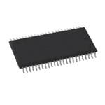
S29AL016J 3. Connection Diagrams Figure 1. 48-pin Standard TSOP (TS048) A15 1 48 A16 A14 2 47 BYTE# A13 3 46 V SS A12 4 45 DQ15/A-1 A11 5 44 DQ7 A10 6 43 DQ14 A9 7 42 DQ6 A8 8 41 DQ13 A19 9 40 DQ5 NC 10 39 DQ12 WE# 11 38 DQ4 RESET# 12 37 V CC NC 13 36 DQ11 WP# 14 35 DQ3 RY/BY# 15 34 DQ10 A18 16 33 DQ2 A17 17 32 DQ9 A7 18 31 DQ1 A6 19 30 DQ8 A5 20 29 DQ0 A4 21 28 OE# A3 22 27 VSS A2 23 26 CE# A1 24 25 A0 Document Number: 002-00777 Rev. *Q Page 5 of 57
S29AL016J Figure 2. 48-ball Fine-pitch BGA (VBK048) (Top View, Balls Facing Down) A6 B6 C6 D6 E6 F6 G6 H6 A13 A12 A14 A15 A16 BYTE# DQ15/A-1 V SS A5 B5 C5 D5 E5 F5 G5 H5 A9 A8 A10 A11 DQ7 DQ14 DQ13 DQ6 A4 B4 C4 D4 E4 F4 G4 H4 WE# RESET# NC A19 DQ5 DQ12 V DQ4 CC A3 B3 C3 D3 E3 F3 G3 H3 RY/BY# WP# A18 NC DQ2 DQ10 DQ11 DQ3 A2 B2 C2 D2 E2 F2 G2 H2 A7 A17 A6 A5 DQ0 DQ8 DQ9 DQ1 A1 B1 C1 D1 E1 F1 G1 H1 A3 A4 A2 A1 A0 CE# OE# V SS Figure 3. 64-ball Fortified BGA (Top View, Balls Facing Down) A8 B8 C8 D8 E8 F8 G8 H8 NC NC NC NC VSS NC NC NC A7 B7 C7 D7 E7 F7 G7 H7 A13 A12 A14 A15 A16 BYTE# DQ15/A-1 VSS A6 B6 C6 D6 E6 F6 G6 H6 A9 A8 A10 A11 DQ7 DQ14 DQ13 DQ6 A5 B5 C5 D5 E5 F5 G5 H5 WE# RESET# NC A19 DQ5 DQ12 VCC DQ4 A4 B4 C4 D4 E4 F4 G4 H4 RY/BY# WP# A18 NC DQ2 DQ10 DQ11 DQ3 A3 B3 C3 D3 E3 F3 G3 H3 A7 A17 A6 A5 DQ0 DQ8 DQ9 DQ1 A2 B2 C2 D2 E2 F2 G2 H2 A3 A4 A2 A1 A0 CE# OE# VSS A1 B1 C1 D1 E1 F1 G1 H1 NC NC NC NC NC NC NC NC Document Number: 002-00777 Rev. *Q Page 6 of 57
S29AL016J 3.1 Special Handling Instructions Special handling is required for Flash Memory products in BGA packages. Flash memory devices in BGA packages may be damaged if exposed to ultrasonic cleaning methods. The package and/or data integrity may be compromised if the package body is exposed to temperatures above 150C for prolonged periods of time. Document Number: 002-00777 Rev. *Q Page 7 of 57
S29AL016J 4. Pin Configuration A0–A19 20 addresses DQ0–DQ14 15 data inputs/outputs DQ15/A-1 DQ15 (data input/output, word mode), A-1 (LSB address input, byte mode) BYTE# Selects 8-bit or 16-bit mode CE# Chip enable OE# Output enable WE# Write enable WP# Write protect: The WP# contains an internal pull-up; when unconnected, WP is at VIH. RESET# Hardware reset RY/BY# Ready/Busy output VCC 3.0 volt-only single power supply (see Section 1. Product Selector Guideon page4 for speed options and voltage supply tolerances) VSS Device ground NC Pin not connected internally 5. Logic Symbol 20 A0–A19 16 or 8 DQ0–DQ15 (A-1) CE# OE# WE# RESET# BYTE# RY/BY# WP# Document Number: 002-00777 Rev. *Q Page 8 of 57
S29AL016J 6. Ordering Information 6.1 S29AL016J Standard Products Cypress standard products are available in several packages and operating ranges. The order number (Valid Combination) is formed by a combination of the elements below. S29AL016J 70 T F I/A 01 0 Packing Type 0 = Tray 2 = 7” Tape and Reel 3 = 13” Tape and Reel Model Number 01 = VCC = 2.7 - 3.6V, top boot sector device (CFI Support) 02 = VCC = 2.7 - 3.6V, bottom boot sector device (CFI Support) 03 = VCC = 2.7 - 3.6V, top boot sector device (No CFI Support) 04 = VCC = 2.7 - 3.6V, bottom boot sector device (No CFI Support) R1 = VCC = 3.0 - 3.6V, top boot sector device (CFI Support) R2 = VCC = 3.0 - 3.6V, bottom boot sector device (CFI Support) Temperature Range I = Industrial (-40°C to +85°C) N = Extended (-40°C to +125°C) A = Automotive, AEC-Q100 Grade 3 (-40°C to +85°C) M = Automotive, AEC-Q100 Grade 1 (-40 °C to +125 °C) Package Material Set F = Pb-Free H = Low-Halogen, Pb-Free Package Type T = Thin Small Outline Package (TSOP) Standard Pinout B = Fine-pitch Ball-Grid Array Package F = Fortified Ball-Grid Array Package Speed Option 55 = 55 ns Access Speed 70 = 70 ns Acess Speed Device Number/Description S29AL016J 16 Megabit Flash Memory manufactured using 110nm process technology 3.0 Volt-only Read, Program, and Erase Notes 2. BGA package marking omits leading “S29” and packing type designator from ordering part number. 3. TSOP package markings omit packing type designator from ordering part number. Document Number: 002-00777 Rev. *Q Page 9 of 57
S29AL016J 6.2 Recommended Combinations Valid Combinations — S29AL016J Valid Combinations list configurations planned to be supported in volume for this device. Consult your local sales office to confirm availability of specific valid combinations and to check on newly released combinations. S29AL016J Valid Combination Package Type, Material, Device Number Speed Option and Temperature Range Model Number Packing Type Package Description TFI, TFN 0, 3 [4] TS048 [6] TSOP 55 BFI, BFN, BHI, BHN R1, R2 VBK048 [7] Fine-Pitch BGA 0, 2, 3 [4] FFI, FFN LAE064 [7] Fortified BGA TFI, TFN 0, 3 [4] TS048 [6] TSOP S29AL016J BFI, BFN, BHI, BHN 01, 02 VBK048 [7] Fine-Pitch BGA 0, 2, 3 [4] 70 FFI, FFN LAE064 [7] Fortified BGA TFI 0, 3 [4] TS048 [6] TSOP 03, 04 BFN, BHN 0, 2, 3 [4] VBK048 [7] Fine-Pitch BGA Notes 4. Type 0 is standard. Specify other options as required. 5. Type 1 is standard. Specify other options as required. 6. TSOP package markings omit packing type designator from ordering part number. 7. BGA package marking omits leading S29 and packing type designator from ordering part number. Valid Combinations — Automotive Grade / AEC-Q100 The table below lists configurations that are Automotive Grade / AEC-Q100 qualified and are planned to be available in volume. The table will be updated as new combinations are released. Consult your local sales representative to confirm availability of specific combinations and to check on newly released combinations. Automotive Grade / AEC-Q100 Valid Combinations Speed Package Type, Material, and Model Package Device Number Option Temperature Range Number Packing Type Description TFA 0, 3 TS048 [9] TSOP 55 BFA, BHA R1, R2 VBK048 [10] Fine-Pitch BGA 0, 2, 3 FFA LAE064 [10] Fortified BGA S29AL016J TFA 0, 3 TS048 [9] TSOP BFA, BHA 01, 02 VBK048 [10] Fine-Pitch BGA 70 0, 2, 3 FFA LAE064 [10] Fortified BGA TFM 02 3 TS048 [10] TSOP Notes 8. Type 0 is standard. Specify other options as required. 9. TSOP package markings omit packing type designator from ordering part number. 10.BGA package marking omits leading S29 and packing type designator from ordering part number. Document Number: 002-00777 Rev. *Q Page 10 of 57
S29AL016J 7. Device Bus Operations This section describes the requirements and use of the device bus operations, which are initiated through the internal command register. The command register itself does not occupy any addressable memory location. The register is composed of latches that store the commands, along with the address and data information needed to execute the command. The contents of the register serve as inputs to the internal state machine. The state machine outputs dictate the function of the device. Table1 lists the device bus operations, the inputs and control levels they require, and the resulting output. The following subsections describe each of these operations in further detail. Table 1. S29AL016J Device Bus Operations DQ8–DQ15 Operation CE# OE# WE# RESET# WP# Addresses [11] DQ0– DQ7 BYTE# = VIH BYTE# = VIL Read L L H H X AIN DOUT DOUT DQ8–DQ14 = High-Z, DQ15 = A-1 Write L H L H [13] AIN [14] [14] Standby VCC 0.3 V X X VCC 0.3 V X X High-Z High-Z High-Z Output Disable L H H H X X High-Z High-Z High-Z Reset X X X L X X High-Z High-Z High-Z Sector Group Sector Address, A6 = L, Protect [12, 13] L H L VID H A3 = A2 = L, A1 = H, A0 = L [14] X X Sector Group Sector Address, A6 = H, Unprotect [12, 13] L H L VID H A3 = A2 = L, A1 = H, A0 = L [14] X X Temporary Sector Group X X X VID H AIN [14] [14] High-Z Unprotect Legend L = Logic Low = VIL; H = Logic High = VIH; VID = 8.5 V to 12.5 V; X = Don’t Care; AIN = Address In; DOUT = Data Out Notes 11.Address In = Amax:A0 in WORD mode (BYTE#=VIH), Address In = Amax:A-1 in BYTE mode (BYTE#=VIL). Sector addresses are Amax to A12 in both WORD mode and BYTE mode. 12.The sector protect and sector unprotect functions may also be implemented via programming equipment. See Section7.10 Sector Group Protection/Unprotection on page 17. 13.If WP# = VIL, the outermost sector remains protected (determined by device configuration). If WP# = VIH, the outermost sector protection depends on whether the sector was last protected or unprotected using the method described in Section7.10 Sector Group Protection/Unprotection on page 17. The WP# contains an internal pull-up; when unconnected, WP is at VIH. 14.DIN or DOUT as required by command sequence, data polling, or sector group protection algorithm. Document Number: 002-00777 Rev. *Q Page 11 of 57
S29AL016J 7.1 Word/Byte Configuration The BYTE# pin controls whether the device data I/O pins DQ15–DQ0 operate in the byte or word configuration. If the BYTE# pin is set at logic 1, the device is in word configuration, DQ15–DQ0 are active and controlled by CE# and OE#. If the BYTE# pin is set at logic 0, the device is in byte configuration, and only data I/O pins DQ0–DQ7 are active and controlled by CE# and OE#. The data I/O pins DQ8–DQ14 are tri-stated, and the DQ15 pin is used as an input for the LSB (A-1) address function. 7.2 Requirements for Reading Array Data To read array data from the outputs, the system must drive the CE# and OE# pins to V . CE# is the power control and selects the IL device. OE# is the output control and gates array data to the output pins. WE# should remain at V . The BYTE# pin determines IH whether the device outputs array data in words or bytes. The internal state machine is set for reading array data upon device power-up, or after a hardware reset. This ensures that no spurious alteration of the memory content occurs during the power transition. No command is necessary in this mode to obtain array data. Standard microprocessor read cycles that assert valid addresses on the device address inputs produce valid data on the device data outputs. The device remains enabled for read access until the command register contents are altered. See Section 10.1 Reading Array Dataon page25 for more information. Refer to the AC Section 17.1 Read Operationson page41 for timing specifications and to Figure15 onpage41 for the timing diagram. I in Section 14. DC Characteristicson page38 CC1 represents the active current specification for reading array data. 7.3 Writing Commands/Command Sequences To write a command or command sequence (which includes programming data to the device and erasing sectors of memory), the system must drive WE# and CE# to V , and OE# to V . IL IH For program operations, the BYTE# pin determines whether the device accepts program data in bytes or words. See Section 7.1 Word/Byte Configurationon page12 for more information. The device features an Unlock Bypass mode to facilitate faster programming. Once the device enters the Unlock Bypass mode, only two write cycles are required to program a word or byte, instead of four. Section 10.5 Word/Byte Program Command Sequenceon page26 has details on programming data to the device using both standard and Unlock Bypass command sequences. An erase operation can erase one sector, multiple sectors, or the entire device. Table2 onpage14 and Table4 onpage15 indicate the address space that each sector occupies. A “sector address” consists of the address bits required to uniquely select a sector. The Section 10. Command Definitionson page25 has details on erasing a sector or the entire chip, or suspending/resuming the erase operation. After the system writes the autoselect command sequence, the device enters the autoselect mode. The system can then read autoselect codes from the internal register (which is separate from the memory array) on DQ7–DQ0. Standard read cycle timings apply in this mode. Refer to Section 7.9 Autoselect Modeon page16 and Section 10.3 Autoselect Command Sequenceon page25 for more information. I in Section 14. DC Characteristicson page38 represents the active current specification for the write mode. Section 17. AC CC2 Characteristicson page41 contains timing specification tables and timing diagrams for write operations. 7.4 Program and Erase Operation Status During an erase or program operation, the system may check the status of the operation by reading the status bits on DQ7–DQ0. Standard read cycle timings and I read specifications apply. Refer to Section 11. Write Operation Statuson page32 for more CC information, and to Section 17. AC Characteristicson page41 for timing diagrams. Document Number: 002-00777 Rev. *Q Page 12 of 57
S29AL016J 7.5 Standby Mode When the system is not reading or writing to the device, it can place the device in the standby mode. In this mode, current consumption is greatly reduced, and the outputs are placed in the high impedance state, independent of the OE# input. The device enters the CMOS standby mode when the CE# and RESET# pins are both held at V 0.3 V. (Note that this is a more CC restricted voltage range than V .) If CE# and RESET# are held at V , but not within V 0.3 V, the device will be in the standby IH IH CC mode, but the standby current will be greater. The device requires standard access time (t ) for read access when the device is in CE either of these standby modes, before it is ready to read data. If the device is deselected during erasure or programming, the device draws active current until the operation is completed. I and I represents the standby current specification shown in the table in Section 14. DC Characteristicson page38. CC3 CC4 7.6 Automatic Sleep Mode The automatic sleep mode minimizes Flash device energy consumption. The device automatically enables this mode when addresses remain stable for t + 30 ns. The automatic sleep mode is independent of the CE#, WE#, and OE# control signals. ACC Standard address access timings provide new data when addresses are changed. While in sleep mode, output data is latched and always available to the system. I in the Section 14. DC Characteristicson page38 represents the automatic sleep mode current CC4 specification. 7.7 RESET#: Hardware Reset Pin The RESET# pin provides a hardware method of resetting the device to reading array data. When the system drives the RESET# pin to V for at least a period of t , the device immediately terminates any operation in progress, tristates all data output pins, and IL RP ignores all read/write attempts for the duration of the RESET# pulse. The device also resets the internal state machine to reading array data. The operation that was interrupted should be reinitiated once the device is ready to accept another command sequence, to ensure data integrity. Current is reduced for the duration of the RESET# pulse. When RESET# is held at V ±0.3V, the device draws CMOS standby SS current (I ). If RESET# is held at V but not within V ±0.3/0.1V, the standby current will be greater. CC4 IL SS The RESET# pin may be tied to the system reset circuitry. A system reset would thus also reset the Flash memory, enabling the system to read the boot-up firmware from the Flash memory. Note that the CE# pin should only go to V after RESET# has gone to IL V . Keeping CE# at V from power up through the first read could cause the first read to retrieve erroneous data. IH IL If RESET# is asserted during a program or erase operation, the RY/BY# pin remains a 0 (busy) until the internal reset operation is complete, which requires a time of t (during Embedded Algorithms). The system can thus monitor RY/BY# to determine READY whether the reset operation is complete. If RESET# is asserted when a program or erase operation is not executing (RY/BY# pin is 1), the reset operation is completed within a time of t (not during Embedded Algorithms). The system can read data t after READY RH the RESET# pin returns to V . IH Refer to the tables in Section 17. AC Characteristicson page41 for RESET# parameters and to Figure16 onpage42 for the timing diagram. 7.8 Output Disable Mode When the OE# input is at V , output from the device is disabled. The output pins are placed in the high impedance state. IH Document Number: 002-00777 Rev. *Q Page 13 of 57
S29AL016J Table 2. Sector Address Tables (Top Boot Device) Sector Size Address Range (in hexadecimal) (Kbytes/ Sector A19 A18 A17 A16 A15 A14 A13 A12 Kwords) Byte Mode (x8) Word Mode (x16) SA0 0 0 0 0 0 X X X 64/32 000000–00FFFF 00000–07FFF SA1 0 0 0 0 1 X X X 64/32 010000–01FFFF 08000–0FFFF SA2 0 0 0 1 0 X X X 64/32 020000–02FFFF 10000–17FFF SA3 0 0 0 1 1 X X X 64/32 030000–03FFFF 18000–1FFFF SA4 0 0 1 0 0 X X X 64/32 040000–04FFFF 20000–27FFF SA5 0 0 1 0 1 X X X 64/32 050000–05FFFF 28000–2FFFF SA6 0 0 1 1 0 X X X 64/32 060000–06FFFF 30000–37FFF SA7 0 0 1 1 1 X X X 64/32 070000–07FFFF 38000–3FFFF SA8 0 1 0 0 0 X X X 64/32 080000–08FFFF 40000–47FFF SA9 0 1 0 0 1 X X X 64/32 090000–09FFFF 48000–4FFFF SA10 0 1 0 1 0 X X X 64/32 0A0000–0AFFFF 50000–57FFF SA11 0 1 0 1 1 X X X 64/32 0B0000–0BFFFF 58000–5FFFF SA12 0 1 1 0 0 X X X 64/32 0C0000–0CFFFF 60000–67FFF SA13 0 1 1 0 1 X X X 64/32 0D0000–0DFFFF 68000–6FFFF SA14 0 1 1 1 0 X X X 64/32 0E0000–0EFFFF 70000–77FFF SA15 0 1 1 1 1 X X X 64/32 0F0000–0FFFFF 78000–7FFFF SA16 1 0 0 0 0 X X X 64/32 100000–10FFFF 80000–87FFF SA17 1 0 0 0 1 X X X 64/32 110000–11FFFF 88000–8FFFF SA18 1 0 0 1 0 X X X 64/32 120000–12FFFF 90000–97FFF SA19 1 0 0 1 1 X X X 64/32 130000–13FFFF 98000–9FFFF SA20 1 0 1 0 0 X X X 64/32 140000–14FFFF A0000–A7FFF SA21 1 0 1 0 1 X X X 64/32 150000–15FFFF A8000–AFFFF SA22 1 0 1 1 0 X X X 64/32 160000–16FFFF B0000–B7FFF SA23 1 0 1 1 1 X X X 64/32 170000–17FFFF B8000–BFFFF SA24 1 1 0 0 0 X X X 64/32 180000–18FFFF C0000–C7FFF SA25 1 1 0 0 1 X X X 64/32 190000–19FFFF C8000–CFFFF SA26 1 1 0 1 0 X X X 64/32 1A0000–1AFFFF D0000–D7FFF SA27 1 1 0 1 1 X X X 64/32 1B0000–1BFFFF D8000–DFFFF SA28 1 1 1 0 0 X X X 64/32 1C0000–1CFFFF E0000–E7FFF SA29 1 1 1 0 1 X X X 64/32 1D0000–1DFFFF E8000–EFFFF SA30 1 1 1 1 0 X X X 64/32 1E0000–1EFFFF F0000–F7FFF SA31 1 1 1 1 1 0 X X 32/16 1F0000–1F7FFF F8000–FBFFF SA32 1 1 1 1 1 1 0 0 8/4 1F8000–1F9FFF FC000–FCFFF SA33 1 1 1 1 1 1 0 1 8/4 1FA000–1FBFFF FD000–FDFFF SA34 1 1 1 1 1 1 1 X 16/8 1FC000–1FFFFF FE000–FFFFF Note 15.Address range is A19:A-1 in byte mode and A19:A0 in word mode. See Section 7.1 Word/Byte Configurationon page12. Table 3. Secured Silicon Sector Addresses (Top Boot) Sector Size (bytes/words) x8 Address Range x16 Address Range 256/128 1FFF00h–1FFFFFh FFF80h–FFFFFh Document Number: 002-00777 Rev. *Q Page 14 of 57
S29AL016J Table 4. Sector Address Tables (Bottom Boot Device) Sector Size Address Range (in hexadecimal) (Kbytes/ Sector A19 A18 A17 A16 A15 A14 A13 A12 Kwords) Byte Mode (x8) Word Mode (x16) SA0 0 0 0 0 0 0 0 X 16/8 000000–003FFF 00000–01FFF SA1 0 0 0 0 0 0 1 0 8/4 004000–005FFF 02000–02FFF SA2 0 0 0 0 0 0 1 1 8/4 006000–007FFF 03000–03FFF SA3 0 0 0 0 0 1 X X 32/16 008000–00FFFF 04000–07FFF SA4 0 0 0 0 1 X X X 64/32 010000–01FFFF 08000–0FFFF SA5 0 0 0 1 0 X X X 64/32 020000–02FFFF 10000–17FFF SA6 0 0 0 1 1 X X X 64/32 030000–03FFFF 18000–1FFFF SA7 0 0 1 0 0 X X X 64/32 040000–04FFFF 20000–27FFF SA8 0 0 1 0 1 X X X 64/32 050000–05FFFF 28000–2FFFF SA9 0 0 1 1 0 X X X 64/32 060000–06FFFF 30000–37FFF SA10 0 0 1 1 1 X X X 64/32 070000–07FFFF 38000–3FFFF SA11 0 1 0 0 0 X X X 64/32 080000–08FFFF 40000–47FFF SA12 0 1 0 0 1 X X X 64/32 090000–09FFFF 48000–4FFFF SA13 0 1 0 1 0 X X X 64/32 0A0000–0AFFFF 50000–57FFF SA14 0 1 0 1 1 X X X 64/32 0B0000–0BFFFF 58000–5FFFF SA15 0 1 1 0 0 X X X 64/32 0C0000–0CFFFF 60000–67FFF SA16 0 1 1 0 1 X X X 64/32 0D0000–0DFFFF 68000–6FFFF SA17 0 1 1 1 0 X X X 64/32 0E0000–0EFFFF 70000–77FFF SA18 0 1 1 1 1 X X X 64/32 0F0000–0FFFFF 78000–7FFFF SA19 1 0 0 0 0 X X X 64/32 100000–10FFFF 80000–87FFF SA20 1 0 0 0 1 X X X 64/32 110000–11FFFF 88000–8FFFF SA21 1 0 0 1 0 X X X 64/32 120000–12FFFF 90000–97FFF SA22 1 0 0 1 1 X X X 64/32 130000–13FFFF 98000–9FFFF SA23 1 0 1 0 0 X X X 64/32 140000–14FFFF A0000–A7FFF SA24 1 0 1 0 1 X X X 64/32 150000–15FFFF A8000–AFFFF SA25 1 0 1 1 0 X X X 64/32 160000–16FFFF B0000–B7FFF SA26 1 0 1 1 1 X X X 64/32 170000–17FFFF B8000–BFFFF SA27 1 1 0 0 0 X X X 64/32 180000–18FFFF C0000–C7FFF SA28 1 1 0 0 1 X X X 64/32 190000–19FFFF C8000–CFFFF SA29 1 1 0 1 0 X X X 64/32 1A0000–1AFFFF D0000–D7FFF SA30 1 1 0 1 1 X X X 64/32 1B0000–1BFFFF D8000–DFFFF SA31 1 1 1 0 0 X X X 64/32 1C0000–1CFFFF E0000–E7FFF SA32 1 1 1 0 1 X X X 64/32 1D0000–1DFFFF E8000–EFFFF SA33 1 1 1 1 0 X X X 64/32 1E0000–1EFFFF F0000–F7FFF SA34 1 1 1 1 1 X X X 64/32 1F0000–1FFFFF F8000–FFFFF Note 16.Address range is A19:A-1 in byte mode and A19:A0 in word mode. See the Section 7.1 Word/Byte Configurationon page12. Table 5. Secured Silicon Sector Addresses (Bottom Boot) Sector Size (bytes/words) x8 Address Range x16 Address Range 256/128 000000h–0000FFh 00000h–0007Fh Document Number: 002-00777 Rev. *Q Page 15 of 57
S29AL016J 7.9 Autoselect Mode The autoselect mode provides manufacturer and device identification, and sector group protection verification, through identifier codes output on DQ7–DQ0. This mode is primarily intended for programming equipment to automatically match a device to be programmed with its corresponding programming algorithm. However, the autoselect codes can also be accessed in-system through the command register. When using programming equipment, the autoselect mode requires V (8.5 V to 12.5 V) on address pin A9. Address pins A6 and ID A3–A0 must be as shown in Table6. In addition, when verifying sector group protection, the sector address must appear on the appropriate highest order address bits (see Table2 onpage14 and Table4 onpage15). Table6 shows the remaining address bits that are don’t care. When all necessary bits have been set as required, the programming equipment may then read the corresponding identifier code on DQ7-DQ0. To access the autoselect codes in-system, the host system can issue the autoselect command via the command register, as shown in Table13 onpage30. This method does not require V . See Section 10. Command Definitionson page25 for details on using the ID autoselect mode. Table 6. S29AL016J Autoselect Codes (HighVoltageMethod) Description Mode CE# OE# WE# A19 to A10 A9 A8 to A7 A6 A5 to A4 A3 to A2 A1 A0 DQ8 to DQ15 DQ7 to DQ0 Manufacturer ID: Cypress L L H X VID X L X L L L X 01h Device ID: S29AL016J Word L L H 22h C4h (Top Boot Block) X VID X L X L L H Byte L L H X C4h Device ID: S29AL016J Word L L H 22h 49h (Bottom Boot Block) X VID X L X L L H Byte L L H X 49h Sector Group Protection X 01h (protected) Verification L L H SA VID X L X L H L X 00h (unprotected) Secured Silicon Sector 8Eh (factory locked) Indicator Bit (DQ7) Top Boot L L H X VID X L X L H H X 0Eh (not factory Block locked) Secured Silicon Sector 96h (factory Indicator Bit (DQ7) Bottom Boot L L H X VID X L X L H H X locked)16h (not Block factory locked) Legend L = Logic Low = VIL; H = Logic High = VIH; SA = Sector Address; X = Don’t care Note 17.The autoselect codes may also be accessed in-system via command sequences. See Table13 onpage30. Document Number: 002-00777 Rev. *Q Page 16 of 57
S29AL016J 7.10 Sector Group Protection/Unprotection The hardware sector group protection feature disables both program and erase operations in any sector group (see Table2 onpage14 to Table4 onpage15). The hardware sector group unprotection feature re-enables both program and erase operations in previously protected sector groups. Sector group protection/unprotection can be implemented via two methods. Sector protection/unprotection requires VID on the RESET# pin only, and can be implemented either in-system or via programming equipment. Figure5 onpage19 shows the algorithms and Figure26 onpage48 shows the timing diagram. This method uses standard microprocessor bus cycle timing. For sector group unprotect, all unprotected sector groups must first be protected prior to the first sector group unprotect write cycle. The device is shipped with all sector groups unprotected. Cypress offers the option of programming and protecting sector groups at its factory prior to shipping the device through Cypress Programming Service. Contact a Cypress representative for details. It is possible to determine whether a sector group is protected or unprotected. See Section 7.9 Autoselect Modeon page16 for details. Table 7. S29AL016J Top Boot Device Sector/Sector Group Protection Sector / Sector Block A19 A18 A17 A16 A15 A14 A13 A12 Sector / Sector Block Size SA0-SA3 0 0 0 X X X X X 256 (4x64) Kbytes SA4-SA7 0 0 1 X X X X X 256 (4x64) Kbytes SA8-SA11 0 1 0 X X X X X 256 (4x64) Kbytes SA12-SA15 0 1 1 X X X X X 256 (4x64) Kbytes SA16-SA19 1 0 0 X X X X X 256 (4x64) Kbytes SA20-SA23 1 0 1 X X X X X 256 (4x64) Kbytes SA24-SA27 1 1 0 X X X X X 256 (4x64) Kbytes SA28-SA29 1 1 1 0 X X X X 128 (2x64) Kbytes SA30 1 1 1 1 0 X X X 64 Kbytes SA31 1 1 1 1 1 0 X X 32 Kbytes SA32 1 1 1 1 1 1 0 0 8 Kbytes SA33 1 1 1 1 1 1 0 1 8 Kbytes SA34 1 1 1 1 1 1 1 X 16 Kbytes Table 8. S29AL016J Bottom Boot Device Sector/Sector Group Protection Sector / Sector Block A19 A18 A17 A16 A15 A14 A13 A12 Sector / Sector Block Size SA0 0 0 0 0 0 0 0 X 16 Kbytes SA1 0 0 0 0 0 0 1 0 8 Kbytes SA2 0 0 0 0 0 0 1 1 8 Kbytes SA3 0 0 0 0 0 1 X X 32 Kbytes SA4 0 0 0 0 1 X X X 64 (1x64) Kbytes SA5-SA6 0 0 0 1 X X X X 128 (2x64) Kbytes SA7-SA10 0 0 1 X X X X X 256 (4x64) Kbytes SA11-SA14 0 1 0 X X X X X 256 (4x64) Kbytes SA15-SA18 0 1 1 X X X X X 256 (4x64) Kbytes SA19-SA22 1 0 0 X X X X X 256 (4x64) Kbytes SA23-SA26 1 0 1 X X X X X 256 (4x64) Kbytes SA27-SA30 1 1 0 X X X X X 256 (4x64) Kbytes SA31-SA34 1 1 1 X X X X X 256 (4x64) Kbytes Document Number: 002-00777 Rev. *Q Page 17 of 57
S29AL016J 7.11 Temporary Sector Group Unprotect This feature allows temporary unprotection of previously protected sector groups to change data in-system. The Sector Group Unprotect mode is activated by setting the RESET# pin to V . During this mode, formerly protected sector groups can be ID programmed or erased by selecting the sector group addresses. Once V is removed from the RESET# pin, all the previously ID protected sector groups are protectedagain. Figure4 shows the algorithm, and Figure25 onpage47 shows the timing diagrams, for this feature. Figure 4. Temporary Sector Group Unprotect Operation START RESET# = VID[18] Perform Erase or Program Operations RESET# = VIH Temporary Sector Group Unprotect Completed [19] Notes 18.All protected sector unprotected. (If WP# = VIL, the highest or lowest address sector remains protected for uniform sector devices; the top or bottom two address sectors remains protected for boot sector devices). 19.All previously protected sector groups are protected once again. Document Number: 002-00777 Rev. *Q Page 18 of 57
S29AL016J Figure 5. In-System Sector Group Protect/Unprotect Algorithms START Protect all sectors: START The indicated portion PLSCNT = 1 of the sector group protect PLSCNT = 1 algorithm must be RESET# = VID performed for all RESET# = VID unprportieocr tteod i ssseucitnogr tghreo ups Wait 1 µs first sector group Wait 1 µs unprotect address First Write No Temporary Sector Cycle = 60h? Group Unprotect Mode Temporary Sector No First Write Group Unprotect Mode Cycle = 60h? Yes Yes No All sectors protected? Set up sector group address Yes Sector Group Protect: Set up first sector Write 60h to sector group group address address with A6 = 0, A3 = A2 = 0, Sector Group Unprotect: A1 = 1, A0 = 0 Write 60h to sector address with A6 = 1, Wait 150 µs A3 = A2 = 0, A1 = 1, A0 = 0 Verify Sector Group Protect: Write 40h Wait 1.5 ms to sector group address with A6 = 0, Verify Sector Group A3 = A2 = 0, Unprotect: Write Increment A1 = 1, A0 = 0 Reset 40h to sector group PLSCNT PLSCNT = 1 address with Read from A6 = 1, sector group address A3 = A2 = 0, with A6 = 0, Increment A1 = 1, A0 = 0 A3 = A2 = 0, PLSCNT A1 = 1, A0 = 0 Read from No sector group address with A6 = 1, No A3 = A2 = 0, PLSCNT Data = 01h? A1 = 1, A0 = 0 = 25? No Set up Yes next sector group Yes PLSCNT No Data = 00h? address = 1000? Yes Protect another Device failed sector group? Yes Yes No Last sector No Remove VID Device failed group verified? from RESET# Yes Wcorimtem reasnedt Sector Group frRoemm RovEeS VEITD # Unprotect Algorithm Sector Group Sector Group Write reset Protect Algorithm Protect complete command Sector Group Unprotect complete Document Number: 002-00777 Rev. *Q Page 19 of 57
S29AL016J 8. Secured Silicon Sector Flash Memory Region The Secured Silicon Sector feature provides a 256-byte Flash memory region that enables permanent part identification through an Electronic Serial Number (ESN). The Secured Silicon Sector uses a Secured Silicon Sector Indicator Bit (DQ7) to indicate whether or not the Secured Silicon Sector is locked when shipped from the factory. This bit is permanently set at the factory and cannot be changed, which prevents cloning of a factory-locked part. This ensures the security of the ESN once the product is shipped to the field. Cypress offers the device with the Secured Silicon Sector either factory-locked or customer-lockable. The factory-locked version is always protected when shipped from the factory, and has the Secured Silicon Sector Indicator Bit permanently set to a 1. The customer-lockable version is shipped with the Secured Silicon Sector unprotected, allowing customers to utilize the that sector in any manner they choose. The customer-lockable version has the Secured Silicon Sector Indicator Bit permanently set to a 0. Thus, the Secured Silicon Sector Indicator Bit prevents customer-lockable devices from being used to replace devices that are factory locked. The system accesses the Secured Silicon Sector through a command sequence (see Section 10.4 Enter/Exit Secured Silicon Sector CommandSequence on page 26). After the system writes the Enter Secured Silicon Sector command sequence, it may read the Secured Silicon Sector by using the addresses normally occupied by the boot sectors. This mode of operation continues until the system issues the Exit Secured Silicon Sector command sequence, or until power is removed from the device. On power-up, or following a hardware reset, the device reverts to sending commands to the boot sectors. 8.1 Factory Locked: Secured Silicon Sector Programmed and Protected at the Factory In a factory locked device, the Secured Silicon Sector is protected when the device is shipped from the factory. The Secured Silicon Sector cannot be modified in any way. The device is available pre-programmed with one of the following: A random, secure ESN only. Customer code through the ExpressFlash service. Both a random, secure ESN and customer code through the ExpressFlash service. In devices that have an ESN, a Bottom Boot device has the 16-byte (8-word) ESN in sector 0 at addresses 00000h–0000Fh in byte mode (or 00000h–00007h in word mode). In the Top Boot device, the ESN is in sector 34 at addresses 1FFFF0h–1FFFFFh in byte mode (or FFFF8h–FFFFFh in word mode). Customers may opt to have their code programmed by Cypress through the Cypress ExpressFlash service. Cypress programs the customer’s code, with or without the random ESN. The devices are then shipped from the Cypress factory with the Secured Silicon Sector permanently locked. Contact a Cypress representative for details on using the Cypress ExpressFlash service. Document Number: 002-00777 Rev. *Q Page 20 of 57
S29AL016J 8.2 Customer Lockable: Secured Silicon Sector NOT Programmed or Protected at the Factory The customer lockable version allows the Secured Silicon Sector to be programmed once, and then permanently locked after it ships from Cypress. Note that the unlock bypass functions is not available when programming the Secured Silicon Sector. The Secured Silicon Sector area can be protected using the following procedures: Write the three-cycle Enter Secured Silicon Region command sequence, and then follow the in-system sector group protect algorithm as shown in Figure 5 on page 19, substituting the sector group address with the Secured Silicon Sector group address (A0=0, A1=1, A2=0, A3=1, A4=1, A5=0, A6=0, A7=0). Note that this method is only applicable to the Secured Silicon Sector. To verify the protect/unprotect status of the Secured Silicon Sector, follow the algorithm shown in Figure 6 on page 21. Once the Secured Silicon Sector is locked and verified, the system must write the Exit Secured Silicon Sector Region command sequence to return to reading and writing the remainder of the array. The Secured Silicon Sector protection must be used with caution since, once protected, there is no procedure available for unprotecting the Secured Silicon Sector area, and none of the bits in the Secured Silicon Sector memory space can be modified in any way. Figure 6. Secured Silicon Sector Protect Verify START If data = 00h, RESET# = V SecSi Sector is ID unprotected. If data = 01h, Wait 1 ms SecSi Sector is protected. Write 60h to any address Remove V ID from RESET# Write 40h to SecSi Sector address with A0=0, A1=1, Write reset A2=0, A3=1, A4=1, command A5=0, A6=0, A7=0 SecSi Sector Read from SecSi Protect Verify Sector address complete with A0=0, A1=1, A2=0, A3=1, A4=1, A5=0, A6=0, A7=0 Document Number: 002-00777 Rev. *Q Page 21 of 57
S29AL016J 9. Common Flash Memory Interface (CFI) The Common Flash Interface (CFI) specification outlines device and host system software interrogation handshake, which allows specific vendor-specified software algorithms to be used for entire families of devices. Software support can then be device- independent, JEDEC ID-independent, and forward- and backward-compatible for the specified flash device families. Flash vendors can standardize their existing interfaces for long-term compatibility. This device enters the CFI Query mode when the system writes the CFI Query command, 98h, to address 55h in word mode (or address AAh in byte mode), any time the device is ready to read array data. The system can read CFI information at the addresses given in Table9 to Table12 onpage23. In word mode, the upper address bits (A7–MSB) must be all zeros. To terminate reading CFI data, the system must write the reset command. The system can also write the CFI query command when the device is in the autoselect mode. The device enters the CFI query mode, and the system can read CFI data at the addresses given in Table9 to Table12 onpage23. The system must write the reset command to return the device to the autoselect mode. Table 9. CFI Query Identification String Addresses Addresses (Word Mode) (Byte Mode) Data Description 10h 20h 0051h 11h 22h 0052h Query Unique ASCII string “QRY” 12h 24h 0059h 13h 26h 0002h Primary OEM Command Set 14h 28h 0000h 15h 2Ah 0040h Address for Primary Extended Table 16h 2Ch 0000h 17h 2Eh 0000h Alternate OEM Command Set (00h = none exists) 18h 30h 0000h 19h 32h 0000h Address for Alternate OEM Extended Table (00h = none exists) 1Ah 34h 0000h Table 10. System Interface String Addresses Addresses (Word Mode) (Byte Mode) Data Description 1Bh 36h 0027h VCC Min. (write/erase) D7–D4: volt, D3–D0: 100 millivolt 1Ch 38h 0036h VCC Max. (write/erase) D7–D4: volt, D3–D0: 100 millivolt 1Dh 3Ah 0000h VPP Min. voltage (00h = no VPP pin present) 1Eh 3Ch 0000h VPP Max. voltage (00h = no VPP pin present) 1Fh 3Eh 0003h Typical timeout per single byte/word write 2N µs 20h 40h 0000h Typical timeout for Min. size buffer write 2N µs (00h = not supported) 21h 42h 0009h Typical timeout per individual block erase 2N ms 22h 44h 0000h Typical timeout for full chip erase 2N ms (00h = not supported) 23h 46h 0005h Max. timeout for byte/word write 2N times typical 24h 48h 0000h Max. timeout for buffer write 2N times typical 25h 4Ah 0004h Max. timeout per individual block erase 2N times typical 26h 4Ch 0000h Max. timeout for full chip erase 2N times typical (00h = not supported) Document Number: 002-00777 Rev. *Q Page 22 of 57
S29AL016J Table 11. Device Geometry Definition Addresses Addresses (Word Mode) (Byte Mode) Data Description 27h 4Eh 0015h Device Size = 2N byte 28h 50h 0002h Flash Device Interface description (refer to CFI publication 100) 29h 52h 0000h 2Ah 54h 0000h Max. number of byte in multi-byte write = 2N (00h = not supported) 2Bh 56h 0000h 2Ch 58h 0004h Number of Erase Block Regions within device 2Dh 5Ah 0000h 2Eh 5Ch 0000h Erase Block Region 1 Information 2Fh 5Eh 0040h (refer to the CFI specification or CFI publication 100) 30h 60h 0000h 31h 62h 0001h 32h 64h 0000h Erase Block Region 2 Information 33h 66h 0020h 34h 68h 0000h 35h 6Ah 0000h 36h 6Ch 0000h Erase Block Region 3 Information 37h 6Eh 0080h 38h 70h 0000h 39h 72h 001Eh 3Ah 74h 0000h Erase Block Region 4 Information 3Bh 76h 0000h 3Ch 78h 0001h Table 12. Primary Vendor-Specific Extended Query Addresses Addresses (Word Mode) (Byte Mode) Data Description 40h 80h 0050h 41h 82h 0052h Query-unique ASCII string “PRI” 42h 84h 0049h 43h 86h 0031h Major version number, ASCII 44h 88h 0033h Minor version number, ASCII Address Sensitive Unlock 0 = Required, 1 = Not Required 45h 8Ah 000Ch Process Technology (Bits 5-2) 0011b = 0.11 µm Floating Gate NOR Erase Suspend 46h 8Ch 0002h 0 = Not Supported, 1 = To Read Only, 2 = To Read & Write Sector Group Protect 47h 8Eh 0001h 0 = Not Supported, X= Number of sectors in smallest sector group Sector Group Temporary Unprotect 48h 90h 0001h 00 = Not Supported, 01 = Supported Sector Group Protect/Unprotect scheme 49h 92h 0004h 01 = 29F040 mode, 02 = 29F016 mode, 03 = 29F400 mode, 04 = 29LV800A mode Simultaneous Operation 4Ah 94h 0000h 00 = Not Supported, 01 = Supported Burst Mode Type 4Bh 96h 0000h 00 = Not Supported, 01 = Supported Page Mode Type 4Ch 98h 0000h 00 = Not Supported, 01 = 4 Word Page, 02 = 8 Word Page ACC (Acceleration) Supply Minimum 4Dh 9Ah 0000h 00 = Not Supported, D7-D4: Volt, D3-D0: 100mV ACC (Acceleration) Supply Maximum 4Eh 9Ch 0000h 00 = Not Supported, D7-D4: Volt, D3-D0: 100mV WP# Protection 00 = Uniform Device without WP Protect 01 = Boot Device with TOP and Bottom WP Protect 02 = Bottom Boot Device with WP Protect 4Fh 9Eh 00XXh 03 = Top Boot Device with WP Protect 04 = Uniform Device with Bottom WP Protect 05 = Uniform Device with Top WP Protect 06 = Uniform Device with All Sectors WP Protect Program Suspend 50h A0h 00XXh 00 = Not Supported, 01 = Supported Document Number: 002-00777 Rev. *Q Page 23 of 57
S29AL016J 9.1 Hardware Data Protection The command sequence requirement of unlock cycles for programming or erasing provides data protection against inadvertent writes (refer to Table13 onpage30 for command definitions). In addition, the following hardware data protection measures prevent accidental erasure or programming, which might otherwise be caused by spurious system level signals during V power-up and CC power-down transitions, or from system noise. 9.1.1 Low V Write Inhibit CC When V is less than V , the device does not accept any write cycles. This protects data during V power-up and power-down. CC LKO CC The command register and all internal program/erase circuits are disabled, and the device resets. Subsequent writes are ignored until V is greater than V . The system must provide the proper signals to the control pins to prevent unintentional writes when CC LKO V is greater than V . CC LKO 9.1.2 Write Pulse Glitch Protection Noise pulses of less than 5 ns (typical) on OE#, CE# or WE# do not initiate a write cycle. 9.1.3 Logical Inhibit Write cycles are inhibited by holding any one of OE# = V , CE# = V or WE# = V . To initiate a write cycle, CE# and WE# must be IL IH IH a logical zero while OE# is a logical one. 9.1.4 Power-Up Write Inhibit If WE# = CE# = V and OE# = V during power up, the device does not accept commands on the rising edge of WE#. The internal IL IH state machine is automatically reset to reading array data on power-up. Document Number: 002-00777 Rev. *Q Page 24 of 57
S29AL016J 10. Command Definitions Writing specific address and data commands or sequences into the command register initiates device operations. Table13 onpage30 defines the valid register command sequences. Writing incorrect address and data values or writing them in the improper sequence resets the device to reading array data. All addresses are latched on the falling edge of WE# or CE#, whichever happens later. All data is latched on the rising edge of WE# or CE#, whichever happens first. Refer to the appropriate timing diagrams in Section 17. AC Characteristicson page41. 10.1 Reading Array Data The device is automatically set to reading array data after device power-up. No commands are required to retrieve data. The device is also ready to read array data after completing an Embedded Program or Embedded Erase algorithm. After the device accepts an Erase Suspend command, the device enters the Erase Suspend mode. The system can read array data using the standard read timings, except that if it reads at an address within erase-suspended sectors, the device outputs status data. After completing a programming operation in the Erase Suspend mode, the system may once again read array data with the same exception. See Section 10.9 Erase Suspend/Erase Resume Commandson page28 for more information on this mode. The system must issue the reset command to re-enable the device for reading array data if DQ5 goes high, or while in the autoselect mode. See Section 10.2 Reset Commandon page25. See also Section 7.2 Requirements for Reading Array Dataon page12 for more information. The Section 17.1 Read Operationson page41 provides the read parameters, and Figure15 onpage41 shows the timing diagram. 10.2 Reset Command Writing the reset command to the device resets the device to reading array data. Address bits are don’t care for this command. The reset command may be written between the sequence cycles in an erase command sequence before erasing begins. This resets the device to reading array data. Once erasure begins, however, the device ignores reset commands until the operation is complete. The reset command may be written between the sequence cycles in a program command sequence before programming begins. This resets the device to reading array data (also applies to programming in Erase Suspend mode). Once programming begins, however, the device ignores reset commands until the operation is complete. The reset command may be written between the sequence cycles in an autoselect command sequence. Once in the autoselect mode, the reset command must be written to return to reading array data (also applies to autoselect during Erase Suspend). If DQ5 goes high during a program or erase operation, writing the reset command returns the device to reading array data (also applies during Erase Suspend). 10.3 Autoselect Command Sequence The autoselect command sequence allows the host system to access the manufacturer and devices codes, and determine whether or not a sector is protected. Table13 onpage30 shows the address and data requirements. This method is an alternative to that shown in Table6 onpage16, which is intended for PROM programmers and requires V on address bit A9. ID The autoselect command sequence is initiated by writing two unlock cycles, followed by the autoselect command. The device then enters the autoselect mode, and the system may read at any address any number of times, without initiating another command sequence. A read cycle at address XX00h retrieves the manufacturer code. A read cycle at address XX01h returns the device code. A read cycle containing a sector address (SA) and the address 02h in word mode (or 04h in byte mode) returns 01h if that sector is protected, or 00h if it is unprotected. Refer to Table2 onpage14 and Table4 onpage15 for valid sector addresses. The system must write the reset command to exit the autoselect mode and return to reading array data. Document Number: 002-00777 Rev. *Q Page 25 of 57
S29AL016J 10.4 Enter/Exit Secured Silicon Sector CommandSequence The Secured Silicon Sector region provides a secured data area containing a random, sixteen-byte electronic serial number (ESN). The system can access the Secured Silicon Sector region by issuing the three-cycle Enter Secured Silicon Sector command sequence. The device continues to access the Secured Silicon Sector region until the system issues the four-cycle Exit Secured Silicon Sector command sequence. The Exit Secured Silicon Sector command sequence returns the device to normal operation. Table13 on page30 shows the addresses and data requirements for both command sequences. Note that the unlock bypass mode is not available when the device enters the Secured Silicon Sector. See also “Secured Silicon Sector Flash Memory Region” on page20 for further information. 10.5 Word/Byte Program Command Sequence The system may program the device by word or byte, depending on the state of the BYTE# pin. Programming is a four-bus-cycle operation. The program command sequence is initiated by writing two unlock write cycles, followed by the program set-up command. The program address and data are written next, which in turn initiate the Embedded Program algorithm. The system is not required to provide further controls or timings. The device automatically generates the program pulses and verifies the programmed cell margin. Table13 onpage30 shows the address and data requirements for the byte program command sequence. When the Embedded Program algorithm is complete, the device then returns to reading array data and addresses are no longer latched. The system can determine the status of the program operation by using DQ7, DQ6, or RY/BY#. See Section 11. Write Operation Statuson page32 for information on these status bits. Any commands written to the device during the Embedded Program Algorithm are ignored. Note that a hardware reset immediately terminates the programming operation. The Byte Program command sequence should be reinitiated once the device has reset to reading array data, to ensure data integrity. Programming is allowed in any sequence and across sector boundaries. A bit cannot be programmed from a 0 back to a 1. Attempting to do so may halt the operation and set DQ5 to 1, or cause the Data# Polling algorithm to indicate the operation was successful. However, a succeeding read will show that the data is still 0. Only erase operations can convert a 0 to a 1. 10.6 Unlock Bypass Command Sequence The unlock bypass feature allows the system to program bytes or words to the device faster than using the standard program command sequence. The unlock bypass command sequence is initiated by first writing two unlock cycles. This is followed by a third write cycle containing the unlock bypass command, 20h. The device then enters the unlock bypass mode. A two-cycle unlock bypass program command sequence is all that is required to program in this mode. The first cycle in this sequence contains the unlock bypass program command, A0h; the second cycle contains the program address and data. Additional data is programmed in the same manner. This mode dispenses with the initial two unlock cycles required in the standard program command sequence, resulting in faster total programming time. Table13 onpage30 shows the requirements for the command sequence. During the unlock bypass mode, only the Unlock Bypass Program and Unlock Bypass Reset commands are valid. To exit the unlock bypass mode, the system must issue the two-cycle unlock bypass reset command sequence. The first cycle must contain the data 90h; the second cycle the data 00h. Addresses are don’t care for both cycles. The device then returns to reading array data. Figure7 onpage27 illustrates the algorithm for the program operation. See Section 17.4 Erase/Program Operationson page44 for parameters, and to Figure19 onpage44 for timing diagrams. Document Number: 002-00777 Rev. *Q Page 26 of 57
S29AL016J Figure 7. Program Operation START Write Program Command Sequence Data Poll from System Embedded Program algorithm in progress Verify Data? No Yes No Increment Address Last Address? Yes Programming Completed Note 20.See Table13 onpage30 for program command sequence. 10.7 Chip Erase Command Sequence Chip erase is a six bus cycle operation. The chip erase command sequence is initiated by writing two unlock cycles, followed by a set-up command. Two additional unlock write cycles are then followed by the chip erase command, which in turn invokes the Embedded Erase algorithm. The device does not require the system to preprogram prior to erase. The Embedded Erase algorithm automatically preprograms and verifies the entire memory for an all zero data pattern prior to electrical erase. The system is not required to provide any controls or timings during these operations. Table13 onpage30 shows the address and data requirements for the chip erase command sequence. Any commands written to the chip during the Embedded Erase algorithm are ignored. Note that a hardware reset during the chip erase operation immediately terminates the operation. The Chip Erase command sequence should be reinitiated once the device has returned to reading array data, to ensure data integrity. The system can determine the status of the erase operation by using DQ7, DQ6, DQ2, or RY/BY#. See Section 11. Write Operation Statuson page32 for information on these status bits. When the Embedded Erase algorithm is complete, the device returns to reading array data and addresses are no longer latched. Figure8 onpage29 illustrates the algorithm for the erase operation. See Section 17.4 Erase/Program Operationson page44 for parameters, and Figure20 onpage45 for timing diagrams. Document Number: 002-00777 Rev. *Q Page 27 of 57
S29AL016J 10.8 Sector Erase Command Sequence Sector erase is a six bus cycle operation. The sector erase command sequence is initiated by writing two unlock cycles, followed by a set-up command. Two additional unlock write cycles are then followed by the address of the sector to be erased, and the sector erase command. Table13 onpage30 shows the address and data requirements for the sector erase command sequence. The device does not require the system to preprogram the memory prior to erase. The Embedded Erase algorithm automatically programs and verifies the sector for an all zero data pattern prior to electrical erase. The system is not required to provide any controls or timings during these operations. After the command sequence is written, a sector erase time-out of 50 µs begins. During the time-out period, additional sector addresses and sector erase commands may be written. However, these additional erase commands are only one bus cycle long and should be identical to the sixth cycle of the standard erase command explained above. Loading the sector erase buffer may be done in any sequence, and the number of sectors may be from one sector to all sectors. The time between these additional cycles must be less than 50 µs, otherwise the last address and command might not be accepted, and erasure may begin. It is recommended that processor interrupts be disabled during this time to ensure all commands are accepted. The interrupts can be re-enabled after the last Sector Erase command is written. If the time between additional sector erase commands can be assumed to be less than 50 µs, the system need not monitor DQ3. Any command other than Sector Erase or Erase Suspend during the time-out period resets the device to reading array data. The system must rewrite the command sequence and any additional sector addresses and commands. The system can monitor DQ3 to determine if the sector erase timer has timed out. (See Section 11.7 DQ3: Sector Erase Timeron page35.) The time-out begins from the rising edge of the final WE# pulse in the command sequence. Once the sector erase operation has begun, only the Erase Suspend command is valid. All other commands are ignored. Note that a hardware reset during the sector erase operation immediately terminates the operation. The Sector Erase command sequence should be reinitiated once the device has returned to reading array data, to ensure data integrity. When the Embedded Erase algorithm is complete, the device returns to reading array data and addresses are no longer latched. The system can determine the status of the erase operation by using DQ7, DQ6, DQ2, or RY/BY#. (Refer to Section 11. Write Operation Statuson page32 for information on these status bits.) Figure8 onpage29 illustrates the algorithm for the erase operation. Refer to Section 17.4 Erase/Program Operationson page44 for parameters, and to Figure20 onpage45 for timing diagrams. 10.9 Erase Suspend/Erase Resume Commands The Erase Suspend command allows the system to interrupt a sector erase operation and then read data from, or program data to, any sector not selected for erasure. This command is valid only during the sector erase operation, including the 50 µs time-out period during the sector erase command sequence. The Erase Suspend command is ignored if written during the chip erase operation or Embedded Program algorithm. Writing the Erase Suspend command during the Sector Erase time-out immediately terminates the time-out period and suspends the erase operation. Addresses are don’t-cares when writing the Erase Suspend command. When the Erase Suspend command is written during a sector erase operation, the device requires a maximum of 35 µs to suspend the erase operation. However, when the Erase Suspend command is written during the sector erase time-out, the device immediately terminates the time-out period and suspends the erase operation. After the erase operation has been suspended, the system can read array data from or program data to any sector not selected for erasure. (The device “erase suspends” all sectors selected for erasure.) Normal read and write timings and command definitions apply. Reading at any address within erase-suspended sectors produces status data on DQ7–DQ0. The system can use DQ7, or DQ6 and DQ2 together, to determine if a sector is actively erasing or is erase-suspended. See Section 11. Write Operation Statuson page32 for information on these status bits. After an erase-suspended program operation is complete, the system can once again read array data within non-suspended sectors. The system can determine the status of the program operation using the DQ7 or DQ6 status bits, just as in the standard program operation. See Section 11. Write Operation Statuson page32 for more information. The system may also write the autoselect command sequence when the device is in the Erase Suspend mode. The device allows reading autoselect codes even at addresses within erasing sectors, since the codes are not stored in the memory array. When the device exits the autoselect mode, the device reverts to the Erase Suspend mode, and is ready for another valid operation. See Section 10.3 Autoselect Command Sequenceon page25 for more information. Document Number: 002-00777 Rev. *Q Page 28 of 57
S29AL016J The system must write the Erase Resume command (address bits are don’t care) to exit the erase suspend mode and continue the sector erase operation. Further writes of the Resume command are ignored. Another Erase Suspend command can be written after the device has resumed erasing. Figure 8. Erase Operation START Write Erase Command Sequence Data Poll from System Embedded Erase algorithm in progress No Data = FFh? Yes Erasure Completed Notes 21.See Table13 onpage30 for erase command sequence. 22.See Section 11.7 DQ3: Sector Erase Timeron page35 for more information. Document Number: 002-00777 Rev. *Q Page 29 of 57
S29AL016J 10.10Command Definitions Table Table 13. S29AL016J Command Definitions Bus Cycles[24-27] s e cl First Second Third Fourth Fifth Sixth y C Command Sequence 1 Addr Data Addr Data Addr Data Addr Data Addr Data Addr Data Read [28] 1 RA RD Reset [29] 1 XXX F0 Word 555 2AA 555 Manufacturer ID 4 AA 55 90 X00 01 Byte AAA 555 AAA Device ID, Word 555 2AA 555 X01 22C4 4 AA 55 90 [30]select TDBooeptvt ioBcmeo o IBDt oB,olot cBkl ock BWByyotteerd 4 AA5AA55AA AA 255A55A55 55 AA5AA55AA 90 XXX000212 2C244949 o ut A (SA) XX00 Word 555 2AA 555 Sector Group Protect X02 XX01 Verify [31] 4 AA 55 90 00 (SA) Byte AAA 555 AAA X04 01 Word 555 2AA 555 Enter Secured Silicon Sector 3 AA 55 88 Byte AAA 555 AAA Word 555 2AA 555 Exit Secured Silicon Sector 4 AA 55 90 XXX 00 Byte AAA 555 AAA Word 55 CFI Query [32] 1 98 Byte AA Word 555 2AA 555 Program 4 AA 55 A0 PA PD Byte AAA 555 AAA Word 555 2AA 555 Unlock Bypass 3 AA 55 20 Byte AAA 555 AAA Unlock Bypass Program [33] 2 XXX A0 PA PD Unlock Bypass Reset [34] 2 XXX 90 XXX 00 Word 555 2AA 555 555 2AA 555 Chip Erase 6 AA 55 80 AA 55 10 Byte AAA 555 AAA AAA 555 AAA Word 555 2AA 555 555 2AA Sector Erase [37] 6 AA 55 80 AA 55 SA 30 Byte AAA 555 AAA AAA 555 Erase Suspend [35] 1 XXX B0 Erase Resume [36] 1 XXX 30 Legend X = Don’t care RA = Address of the memory location to be read RD = Data read from location RA during read operation. PA = Address of the memory location to be programmed. Addresses latch on the falling edge of the WE# or CE# pulse, whichever happens later. PD = Data to be programmed at location PA. Data latches on the rising edge of WE# or CE# pulse, whichever happens first. SA = Address of the sector to be verified (in autoselect mode) or erased. Address bits A19–A12 uniquely select any sector. Notes 23.See Table1 on page11 for description of bus operations. 24.All values are in hexadecimal. 25.Except for the read cycle and the fourth cycle of the autoselect command sequence, all bus cycles are write cycles. 26.Data bits DQ15–DQ8 are don’t cares for unlock and command cycles. 27.Address bits A19–A11 are don’t cares for unlock and command cycles, unless SA or PA required. 28.No unlock or command cycles required when reading array data. 29.The Reset command is required to return to reading array data when device is in the autoselect mode, or if DQ5 goes high (while the device is providing status data). 30.The fourth cycle of the autoselect command sequence is a read cycle. 31.The data is 00h for an unprotected sector and 01h for a protected sector. See “Section 10.3 Autoselect Command Sequence on page 25” for more information. Document Number: 002-00777 Rev. *Q Page 30 of 57
S29AL016J 32.Command is valid when device is ready to read array data or when device is in autoselect mode. 33.The Unlock Bypass command is required prior to the Unlock Bypass Program command. 34.The Unlock Bypass Reset command is required to return to reading array data when the device is in the unlock bypass mode. F0 is also acceptable. 35.The system may read and program in non-erasing sectors, or enter the autoselect mode, when in the Erase Suspend mode. The Erase Suspend command is valid only during a sector erase operation. 36.The Erase Resume command is valid only during the Erase Suspend mode. 37.Additional sector erase commands during the time-out period after an initial sector erase are one cycle long and identical to the sixth cycle of the sector erase command sequence (SA / 30). Document Number: 002-00777 Rev. *Q Page 31 of 57
S29AL016J 11. Write Operation Status The device provides several bits to determine the status of a write operation: DQ2, DQ3, DQ5, DQ6, DQ7, and RY/BY#. Table14 onpage35 and the following subsections describe the functions of these bits. DQ7, RY/BY#, and DQ6 each offer a method for determining whether a program or erase operation is complete or in progress. These three bits are discussed first. 11.1 DQ7: Data# Polling The Data# Polling bit, DQ7, indicates to the host system whether an Embedded Algorithm is in progress or completed, or whether the device is in Erase Suspend. Data# Polling is valid after the rising edge of the final WE# pulse in the program or erase command sequence. During the Embedded Program algorithm, the device outputs on DQ7 the complement of the datum programmed to DQ7. This DQ7 status also applies to programming during Erase Suspend. When the Embedded Program algorithm is complete, the device outputs the datum programmed to DQ7. The system must provide the program address to read valid status information on DQ7. If a program address falls within a protected sector, Data# Polling on DQ7 is active for approximately 1 µs, then the device returns to reading array data. During the Embedded Erase algorithm, Data# Polling produces a 0 on DQ7. When the Embedded Erase algorithm is complete, or if the device enters the Erase Suspend mode, Data# Polling produces a 1 on DQ7. This is analogous to the complement/true datum output described for the Embedded Program algorithm: the erase function changes all the bits in a sector to 1; prior to this, the device outputs the complement, or 0. The system must provide an address within any of the sectors selected for erasure to read valid status information on DQ7. After an erase command sequence is written, if all sectors selected for erasing are protected, Data# Polling on DQ7 is active for approximately 100 µs, then the device returns to reading array data. If not all selected sectors are protected, the Embedded Erase algorithm erases the unprotected sectors, and ignores the selected sectors that are protected. When the system detects DQ7 has changed from the complement to true data, it can read valid data at DQ7–DQ0 on the following read cycles. This is because DQ7 may change asynchronously with DQ0–DQ6 while Output Enable (OE#) is asserted low. Figure22 onpage46, illustrates this. Table14 onpage35 shows the outputs for Data# Polling on DQ7. Figure10 onpage34 shows the Data# Polling algorithm. Figure 9. Data# Polling Algorithm START Read DQ7–DQ0 Addr = VA DQ7 = Data? Yes No No DQ5 = 1? Yes Read DQ7–DQ0 Addr = VA Yes DQ7 = Data? No FAIL PASS Document Number: 002-00777 Rev. *Q Page 32 of 57
S29AL016J Notes 38.VA = Valid address for programming. During a sector erase operation, a valid address is an address within any sector selected for erasure. During chip erase, a valid address is any non-protected sector address. 39.DQ7 should be rechecked even if DQ5 = 1 because DQ7 may change simultaneously with DQ5. 11.2 RY/BY#: Ready/Busy# The RY/BY# is a dedicated, open-drain output pin that indicates whether an Embedded Algorithm is in progress or complete. The RY/BY# status is valid after the rising edge of the final WE# pulse in the command sequence. Since RY/BY# is an open-drain output, several RY/BY# pins can be tied together in parallel with a pull-up resistor to V . CC If the output is low (Busy), the device is actively erasing or programming. (This includes programming in the Erase Suspend mode.) If the output is high (Ready), the device is ready to read array data (including during the Erase Suspend mode), or is in the standby mode. Table14 onpage35 shows the outputs for RY/BY#. Figures Figure15 onpage41, Figure16 onpage42, Figure19 onpage44 and Figure20 onpage45 shows RY/BY# for read, reset, program, and erase operations, respectively. 11.3 DQ6: Toggle Bit I Toggle Bit I on DQ6 indicates whether an Embedded Program or Erase algorithm is in progress or complete, or whether the device has entered the Erase Suspend mode. Toggle Bit I may be read at any address, and is valid after the rising edge of the final WE# pulse in the command sequence (prior to the program or erase operation), and during the sector erase time-out. During an Embedded Program or Erase algorithm operation, successive read cycles to any address cause DQ6 to toggle. (The system may use either OE# or CE# to control the read cycles.) When the operation is complete, DQ6 stops toggling. After an erase command sequence is written, if all sectors selected for erasing are protected, DQ6 toggles for approximately 100 µs, then returns to reading array data. If not all selected sectors are protected, the Embedded Erase algorithm erases the unprotected sectors, and ignores the selected sectors that are protected. The system can use DQ6 and DQ2 together to determine whether a sector is actively erasing or is erase-suspended. When the device is actively erasing (that is, the Embedded Erase algorithm is in progress), DQ6 toggles. When the device enters the Erase Suspend mode, DQ6 stops toggling. However, the system must also use DQ2 to determine which sectors are erasing or erase- suspended. Alternatively, the system can use DQ7 (see Section 11.1 DQ7: Data# Pollingon page32). If a program address falls within a protected sector, DQ6 toggles for approximately 1 µs after the program command sequence is written, then returns to reading array data. DQ6 also toggles during the erase-suspend-program mode, and stops toggling once the Embedded Program algorithm is complete. Table14 onpage35 shows the outputs for Toggle Bit I on DQ6. Figure10 onpage34 shows the toggle bit algorithm in flowchart form, and Section 11.5 Reading Toggle Bits DQ6/DQ2on page34 explains the algorithm. Figure23 onpage46 shows the toggle bit timing diagrams. Figure24 onpage47 shows the differences between DQ2 and DQ6 in graphical form. See also the subsection on Section 11.4 DQ2: Toggle Bit IIon page33. 11.4 DQ2: Toggle Bit II The “Toggle Bit II” on DQ2, when used with DQ6, indicates whether a particular sector is actively erasing (that is, the Embedded Erase algorithm is in progress), or whether that sector is erase-suspended. Toggle Bit II is valid after the rising edge of the final WE# pulse in the command sequence. DQ2 toggles when the system reads at addresses within those sectors that have been selected for erasure. (The system may use either OE# or CE# to control the read cycles.) But DQ2 cannot distinguish whether the sector is actively erasing or is erase- suspended. DQ6, by comparison, indicates whether the device is actively erasing, or is in Erase Suspend, but cannot distinguish which sectors are selected for erasure. Thus, both status bits are required for sector and mode information. Refer to Table14 onpage35 to compare outputs for DQ2 and DQ6. Figure10 onpage34 shows the toggle bit algorithm in flowchart form, and the section Section 11.5 Reading Toggle Bits DQ6/ DQ2on page34 explains the algorithm. See also the Section 11.3 DQ6: Toggle Bit Ion page33 subsection. Figure23 onpage46 shows the toggle bit timing diagram. Figure24 onpage47 shows the differences between DQ2 and DQ6 in graphical form. Document Number: 002-00777 Rev. *Q Page 33 of 57
S29AL016J 11.5 Reading Toggle Bits DQ6/DQ2 Refer to Figure10 onpage34 for the following discussion. Whenever the system initially begins reading toggle bit status, it must read DQ7–DQ0 at least twice in a row to determine whether a toggle bit is toggling. Typically, the system would note and store the value of the toggle bit after the first read. After the second read, the system would compare the new value of the toggle bit with the first. If the toggle bit is not toggling, the device has completed the program or erase operation. The system can read array data on DQ7–DQ0 on the following read cycle. However, if after the initial two read cycles, the system determines that the toggle bit is still toggling, the system also should note whether the value of DQ5 is high (see the section on DQ5). If it is, the system should then determine again whether the toggle bit is toggling, since the toggle bit may have stopped toggling just as DQ5 went high. If the toggle bit is no longer toggling, the device has successfully completed the program or erase operation. If it is still toggling, the device did not complete the operation successfully, and the system must write the reset command to return to reading array data. The remaining scenario is that the system initially determines that the toggle bit is toggling and DQ5 has not gone high. The system may continue to monitor the toggle bit and DQ5 through successive read cycles, determining the status as described in the previous paragraph. Alternatively, it may choose to perform other system tasks. In this case, the system must start at the beginning of the algorithm when it returns to determine the status of the operation (top of Figure10 onpage34). Figure 10. Toggle Bit Algorithm START [40] Read DQ7–DQ0 Read DQ7–DQ0 Toggle Bit No = Toggle? Yes No DQ5 = 1? Yes Read DQ7–DQ0 [40, 41] Twice Toggle Bit No = Toggle? Yes Program/Erase Operation Not Program/Erase Complete, Write Operation Complete Reset Command Notes 40.Read toggle bit twice to determine whether or not it is toggling. See text. 41.Recheck toggle bit because it may stop toggling as DQ5 changes to 1. See text. Document Number: 002-00777 Rev. *Q Page 34 of 57
S29AL016J 11.6 DQ5: Exceeded Timing Limits DQ5 indicates whether the program or erase time has exceeded a specified internal pulse count limit. Under these conditions DQ5 produces a 1. This is a failure condition that indicates the program or erase cycle was not successfully completed. The DQ5 failure condition may appear if the system tries to program a 1 to a location that is previously programmed to 0. Only an erase operation can change a 0 back to a 1. Under this condition, the device halts the operation, and when the operation has exceeded the timing limits, DQ5 produces a 1. Under both these conditions, the system must issue the reset command to return the device to reading array data. 11.7 DQ3: Sector Erase Timer After writing a sector erase command sequence, the system may read DQ3 to determine whether or not an erase operation has begun. (The sector erase timer does not apply to the chip erase command.) If additional sectors are selected for erasure, the entire time-out also applies after each additional sector erase command. When the time-out is complete, DQ3 switches from 0 to 1. The system may ignore DQ3 if the system can guarantee that the time between additional sector erase commands will always be less than 50 s. See also Section 10.8 Sector Erase Command Sequenceon page28. After the sector erase command sequence is written, the system should read the status on DQ7 (Data# Polling) or DQ6 (Toggle Bit I) to ensure the device has accepted the command sequence, and then read DQ3. If DQ3 is 1, the internally controlled erase cycle has begun; all further commands (other than Erase Suspend) are ignored until the erase operation is complete. If DQ3 is 0, the device will accept additional sector erase commands. To ensure the command has been accepted, the system software should check the status of DQ3 prior to and following each subsequent sector erase command. If DQ3 is high on the second status check, the last command might not have been accepted. Table14 shows the outputs for DQ3. Table 14. Write Operation Status Operation DQ7[43] DQ6 DQ5 [42] DQ3 DQ2 [43] RY/BY# Standard Embedded Program Algorithm DQ7# Toggle 0 N/A No toggle 0 Mode Embedded Erase Algorithm 0 Toggle 0 1 Toggle 0 Reading within Erase Suspended Sector 1 No toggle 0 N/A Toggle 1 Erase Reading within Non-Erase Suspended Suspend Data Data Data Data Data 1 Sector Mode Erase-Suspend-Program DQ7# Toggle 0 N/A N/A 0 Notes 42.DQ5 switches to 1 when an Embedded Program or Embedded Erase operation has exceeded the maximum timing limits. See Section 11.6 DQ5: Exceeded Timing Limitson page35 for more information. 43.DQ7 and DQ2 require a valid address when reading status information. Refer to the appropriate subsection for further details. Document Number: 002-00777 Rev. *Q Page 35 of 57
S29AL016J 12. Absolute Maximum Ratings Parameter Rating Storage Temperature Plastic Packages –65°C to +150°C Ambient Temperature with Power Applied –65°C to +125°C Voltage with Respect to Ground VCC [44] –0.5 V to +4.0 V A9, OE#, and RESET# [45] –0.5 V to +12.5 V All other pins[44] –0.5 V to VCC+0.5 V Output Short Circuit Current [46] 200 mA Notes 44.Minimum DC voltage on input or I/O pins is –0.5 V. During voltage transitions, input or I/O pins may overshoot VSS to –2.0 V for periods of up to 20 ns. See Figure11 onpage37. Maximum DC voltage on input or I/O pins is VCC +0.5 V. During voltage transitions, input or I/O pins may overshoot to VCC +2.0 V for periods up to 20 ns. See Figure12 onpage37. 45.Minimum DC input voltage on pins A9, OE#, and RESET# is -0.5 V. During voltage transitions, A9, OE#, and RESET# may overshoot VSS to –2.0 V for periods of up to 20 ns. See Figure11 onpage37. Maximum DC input voltage on pin A9 is +12.5 V which may overshoot to 14.0 V for periods up to 20 ns. 46.No more than one output may be shorted to ground at a time. Duration of the short circuit should not be greater than one second. 47.Stresses above those listed under Absolute Maximum Ratings may cause permanent damage to the device. This is a stress rating only; functional operation of the device at these or any other conditions above those indicated in the operational sections of this data sheet is not implied. Exposure of the device to absolute maximum rating conditions for extended periods may affect device reliability. Document Number: 002-00777 Rev. *Q Page 36 of 57
S29AL016J 13. Operating Ranges Parameter Range Industrial (I) Devices –40°C to +85°C Automotive (A) Devices –40°C to +85°C Ambient Temperature Extended (N) Devices –40°C to +125°C Automotive (M) Devices –40°C to +125°C Full 2.7 V to 3.6 V VCC Supply Voltages Regulated 3.0 V to 3.6 V Note 48.Operating ranges define those limits between which the functionality of the device is guaranteed. Figure 11. Maximum Negative OvershootWaveform 20 ns 20 ns +0.8 V –0.5 V –2.0 V 20 ns Figure 12. Maximum Positive OvershootWaveform 20 ns V CC V CC 2.0 V 20 ns Document Number: 002-00777 Rev. *Q Page 37 of 57
S29AL016J 14. DC Characteristics 14.1 CMOS Compatible Parameter Description Test Conditions Min Typ Max Unit Input Load Current VIN = VSS to VCC, VCC = VCC max – – 1.0 ILI WP# Input Load Current VCC = VCC max, WP# = VSS to VCC – – 25 µA ILIT A9 Input Load Current VCC = VCC max; A9 = 12.5 V – – 35 ILO Output Leakage Current VOUT = VSS to VCC, VCC = VCC max – – 1.0 5 MHz – 7 12 CE# = VIL, OE# = VIH, VCC = VCC max, Byte Mode 1 MHz – 2 4 ICC1 VCC Active Read Current [49] mA 5 MHz – 7 12 CE# = VIL, OE# = VIH,, VCC = VCC max, Word Mode 1 MHz – 2 4 ICC2 VCC Active Erase/Program Current [50, 51, 52] CVCEC# == VVCILC, OmEax# = VIH, – 20 30 mA OE# = VIH, ICC3 VCC Standby Current [52] CE#, RESET# = VCC + 0.3 V/-0.1V, – 0.2 5 µA WP# = VCC or open, VCC = VCC max [53] VCC = VCC max; ICC4 VCC Standby Current During Reset [52] RESET# = VSS + 0.3 V/-0.1V – 0.2 5 µA WP# = VCC or open, [53] VCC = VCC max, VIH = VCC + 0.3 V, ICC5 Automatic Sleep Mode [51], [52] VIL = VSS + 0.3 V/-0.1 V, – 0.2 5 µA WP# = VCC or open, [53] VIL Input Low Voltage -0.1 0.8 – VIH Input High Voltage 0.7 x VCC VCC + 0.3 Voltage for Autoselect and Temporary Sector VID Unprotect VCC = 2.7–3.6 V 8.5 12.5 – V VOL Output Low Voltage IOL = 4.0 mA, VCC = VCC min – 0.45 VOH1 IOH = -2.0 mA, VCC = VCC min 0.85 x VCC – Output High Voltage VOH2 IOH = -100 µA, VCC = VCC min VCC–0.4 – VLKO Low VCC Lock-Out Voltage – 2.1 2.5 Notes 49.The ICC current listed is typically less than 2 mA/MHz, with OE# at VIH. Typical VCC is 3.0 V. 50.ICC active while Embedded Erase or Embedded Program is in progress. 51.Automatic sleep mode enables the low power mode when addresses remain stable for tACC + 30 ns. 52.Not 100% tested. 53.When the device is operated in Extended Temperature range, the currents are as follows: ICC3 = 0.2 µA (typ), 10 µA (max) ICC4 = 0.2 µA (typ), 10 µA (max) ICC5 = 0.2 µA (typ), 10 µA (max) Document Number: 002-00777 Rev. *Q Page 38 of 57
S29AL016J 15. Test Conditions Figure 13. Test Setup 3.3 V 2.7 k Device Under Test CL 6.2 k Note 54.Diodes are IN3064 or equivalent. Table 15. Test Specifications Test Condition 70 55 Unit Output Load 1 TTL gate Output Load Capacitance, CL (including jig capacitance) 30 pF Input Rise and Fall Times 5 ns Input Pulse Levels 0.0 or VCC Input timing measurement reference levels 0.5 VCC V Output timing measurement reference levels 0.5 VCC Document Number: 002-00777 Rev. *Q Page 39 of 57
S29AL016J 16. Key to Switching Waveforms Waveform Inputs Outputs Steady Changing from H to L Changing from L to H Don’t Care, Any Change Permitted Changing, State Unknown Does Not Apply Center Line is High Impedance State (High Z) Figure 14. Input Waveforms and Measurement Levels V CC Input 0.5 V Measurement Level 0.5 V Output CC CC 0.0 V Document Number: 002-00777 Rev. *Q Page 40 of 57
S29AL016J 17. AC Characteristics 17.1 Read Operations Parameter Speed Options JEDEC Std Description Test Setup 70 55 Unit tAVAV tRC Read Cycle Time [55] Min 70 55 tAVQV tACC Address to Output Delay OCEE## == VVIILL Max 70 55 tELQV tCE Chip Enable to Output Delay OE# = VIL Max 70 55 tGLQV tOE Output Enable to Output Delay – Max 30 30 tEHQZ tDF Chip Enable to Output High Z [55] – Max 16 ns tGHQZ tDF Output Enable to Output High Z [55] – Max 16 – tSR/W Latency Between Read and Write Operations – Min 20 Read – Min 0 – tOEH Output Enable Hold Time [55] Toggle and Data# Polling – Min 10 Output Hold Time From Addresses, CE# or OE#, Whichever tAXQX tOH Occurs First [55] – Min 0 Notes 55.Not 100% tested. 56.See Figure13 onpage39 and Table15 onpage39 for test specifications. Figure 15. Read Operations Timings tRC Addresses Addresses Stable tACC CE# tDF OE# tSR/W tOE tOEH WE# tCE tOH HIGH Z HIGH Z Outputs Output Valid RESET# RY/BY# 0 V Document Number: 002-00777 Rev. *Q Page 41 of 57
S29AL016J 17.2 Hardware Reset (RESET#) Parameter JEDEC Std Description Test Setup All Speed Options Unit tREADY RESET# Pin Low (During Embedded Algorithms) to Read or Write [57] Max 35 µs RESET# Pin Low (NOT During Embedded Algorithms) to Read or tREADY Write [57] Max 500 ns tRP RESET# Pulse Width 500 tRH RESET# High Time Before Read [57] 50 Min tRPD RESET# Low to Standby Mode 35 µs tRB RY/BY# Recovery Time 0 ns Note 57.Not 100% tested. Figure 16. RESET# Timings RY/BY# CE#, OE# tRH RESET# tRP tReady [58] Reset Timings NOT during Embedded Algorithms (Note 1) Reset Timings during Embedded Algorithms tReady RY/BY# tRB CE#, OE# RESET# tRP Note 58.CE# should only go low after RESET# has gone high. Keeping CE# low from power up through the first read could cause the first read to retrieve erroneous data. Document Number: 002-00777 Rev. *Q Page 42 of 57
S29AL016J 17.3 Word/Byte Configuration (BYTE#) Parameter Speed Options JEDEC Std Description 70 55 Unit tELFL/tELFH CE# to BYTE# Switching Low or High Max 5 tFLQZ BYTE# Switching Low to Output HIGH Z Max 16 ns tFHQV BYTE# Switching High to Output Active Min 70 55 Figure 17. BYTE# Timings for Read Operations CE# OE# BYTE# tELFL BYTE# DQ0–DQ14 Data Output Data Output (DQ0–DQ14) (DQ0–DQ7) Switching from word to byte mode DQ15/A-1 ODuQtp1u5t AdIndpreusts tFLQZ tELFH BYTE# BYTE# Switching from byte to DQ0–DQ14 D(DaQta0 O–DuQtp7u)t (DDaQta0 –ODuQtp1u4t) word mode DQ15/A-1 Address DQ15 Input Output tFHQV Figure 18. BYTE# Timings for Write Operations CE# The falling edge of the last WE# signal WE# BYTE# t SET (t ) AS t (t ) HOLD AH Note 59.Refer to the Erase/Program Operations table for tAS and tAH specifications. Document Number: 002-00777 Rev. *Q Page 43 of 57
S29AL016J 17.4 Erase/Program Operations Parameter Speed Options JEDEC Std Description 70 55 Unit tAVAV tWC Write Cycle Time 60 Min 70 55 ns tAVWL tAS Address Setup Time Min 0 ns tWLAX tAH Address Hold Time Min 45 ns tDVWH tDS Data Setup Time Min 35 35 ns tWHDX tDH Data Hold Time Min 0 ns tOES Output Enable Setup Time Min 0 ns tGHWL tGHWL Read Recovery Time Before Write (OE# High to WE# Low) Min 0 ns tELWL tCS CE# Setup Time Min 0 ns tWHEH tCH CE# Hold Time Min 0 ns tWLWH tWP Write Pulse Width Min 35 35 ns tWHWL tWPH Write Pulse Width High Min 25 ns tSR/W Latency Between Read and Write Operations Min 20 ns Byte Typ 6 tWHWH1 tWHWH1 Programming Operation [61] µs Word Typ 6 tWHWH2 tWHWH2 Sector Erase Operation [61] Typ 0.5 sec tVCS VCC Setup Time [60] Min 50 µs tRB Recovery Time from RY/BY# Min 0 ns tBUSY Program/Erase Valid to RY/BY# Delay Max 90 Notes 60.Not 100% tested. 61.See Section 18. Erase and Programming Performanceon page50 for more information. Figure 19. Program Operation Timings Program Command Sequence (last two cycles) Read Status Data (last two cycles) tWC tAS Addresses 555h PA PA PA tAH CE# tCH OE# tWP tWHWH1 WE# tCS tWPH tDS tDH Data A0h PD Status DOUT tBUSY tRB RY/BY# tVCS VCC Notes 62.PA = program address, PD = program data, DOUT is the true data at the program address. 63.Illustration shows device in word mode. Document Number: 002-00777 Rev. *Q Page 44 of 57
S29AL016J Figure 20. Chip/Sector Erase Operation Timings Erase Command Sequence (last two cycles) Read Status Data tWC tAS Addresses 2AAh SA VA VA 555h for chip erase t AH CE# OE# tCH t WP WE# t tWPH tWHWH2 CS t DS t DH Data 55h 30h ProgInress Complete 10 for Chip Erase tBUSY tRB RY/BY# t VCS V CC Notes 64.SA = sector address (for Sector Erase), VA = Valid Address for reading status data (see Section 11. Write Operation Statuson page32). 65.Illustration shows device in word mode. Figure 21. Back to Back Read/Write Cycle Timing tWC tRC tWC tWC Addresses Valid PA Valid RA Valid PA Valid PA tAH tACC tCPH CE# tCE tOE tCP OE# tOEH tGHWL tWP WE# tDF tWPH tDS tDH tOH Data Valid Valid Valid Valid In Out In In tSR/W WE# Controlled Write Cycle Read Cycle CE# Controlled Write Cycles Document Number: 002-00777 Rev. *Q Page 45 of 57
S29AL016J Figure 22. Data# Polling Timings (DuringEmbeddedAlgorithms) tRC Addresses VA VA VA tACC tCE CE# tCH tOE OE# tOEH tDF WE# tOH High Z DQ7 Complement Complement True Valid Data High Z DQ0–DQ6 Status Data Status Data True Valid Data tBUSY RY/BY# Notes 66.VA = Valid address. Illustration shows first status cycle after command sequence, last status read cycle, and array data read cycle. Figure 23. Toggle Bit Timings (DuringEmbeddedAlgorithms) tRC Addresses VA VA VA VA tACC tCE CE# tCH tOE OE# tOEH tDF WE# tOH DQ6/DQ2 High Z Valid Status Valid Status Valid Status Valid Data (first read) (second read) (stops toggling) tBUSY RY/BY# Note 67.VA = Valid address; not required for DQ6. Illustration shows first two status cycle after command sequence, last status read cycle, and array data read cycle. Document Number: 002-00777 Rev. *Q Page 46 of 57
S29AL016J Figure 24. DQ2 vs. DQ6 for Erase and EraseSuspendOperations Enter Embedded Erase Enter Erase Erase Erasing Suspend Suspend Program Resume WE# Erase Erase Suspend Erase Erase Suspend Erase Erase Read Suspend Read Complete Program DQ6 DQ2 Note 68.The system may use CE# or OE# to toggle DQ2 and DQ6. DQ2 toggles only when read at an address within an erase-suspended sector. 17.5 Temporary Sector Group Unprotect Parameter JEDEC Std Description All Speed Options Unit tVIDR VID Rise and Fall Time [69] Min 500 ns tRSP RESET# Setup Time for Temporary Sector Unprotect Min 4 µs RESET# Hold Time from RY/BY# High for Temporary Sector tRRB Unprotect Min 4 µs Note 69.Not 100% tested. Figure 25. Temporary Sector Group Unprotect/TimingDiagram 12V RESET# 0 or 3V t t VIDR VIDR Program or Erase Command Sequence CE# WE# tRSP tRRB RY/BY# Document Number: 002-00777 Rev. *Q Page 47 of 57
S29AL016J Figure 26. Sector Group Protect/Unprotect TimingDiagram VID VIH RESET# SA, A6, A3, A2 Valid* Valid* Valid* A1, A0 Sector Group Protect/Unprotect Verify Data 60h 60h 40h Status 1 µs Sector Group Protect: 150 µs Sector Group Unprotect: 1.5 ms CE# WE# OE# Note 70.For sector group protect, A6 = 0, A3 = A2 = 0, A1 = 1, A0 = 0. For sector group unprotect, A6 = 1, A3 = A2 = 0, A1 = 1, A0 = 0. Document Number: 002-00777 Rev. *Q Page 48 of 57
S29AL016J 17.6 Alternate CE# Controlled Erase/Program Operations Parameter Speed Options JEDEC Std Description 70 55 Unit tAVAV tWC Write Cycle Time [71] Min 70 55 ns tAVEL tAS Address Setup Time Min 0 ns tELAX tAH Address Hold Time Min 45 ns tDVEH tDS Data Setup Time Min 35 35 ns tEHDX tDH Data Hold Time Min 0 ns tOES Output Enable Setup Time Min 0 ns tGHEL tGHEL Read Recovery Time Before Write (OE# High to WE# Low) Min 0 ns tWLEL tWS WE# Setup Time Min 0 ns tEHWH tWH WE# Hold Time Min 0 ns tELEH tCP CE# Pulse Width Min 35 35 ns tEHEL tCPH CE# Pulse Width High Min 25 ns tSR/W Latency Between Read and Write Operations Min 20 ns Byte Typ 6 tWHWH1 tWHWH1 Programming Operation [72] µs Word Typ 6 tWHWH2 tWHWH2 Sector Erase Operation [72] Typ 0.5 sec Notes 71.Not 100% tested. 72.See Section 18. Erase and Programming Performanceon page50 for more information. Figure 27. Alternate CE# Controlled Write OperationTimings 555 for program PA for program 2AA for erase SA for sector erase 555 for chip erase Data# Polling Addresses PA tWC tAS tAH tWH WE# tGHEL OE# tCP tWHWH1 or 2 CE# tWS tCPH tDS tBUSY tDH Data DQ7# DOUT tRH A0 for program PD for program 55 for erase 30 for sector erase 10 for chip erase RESET# RY/BY# Notes 73.PA = program address, PD = program data, DQ7# = complement of the data written to the device, DOUT = data written to the device. 74.Figure indicates the last two bus cycles of the command sequence. 75.Word mode address used as an example. Document Number: 002-00777 Rev. *Q Page 49 of 57
S29AL016J 18. Erase and Programming Performance Parameter Typ [76] Max [77] Unit Comments Sector Erase Time 0.5 10 s Excludes 00h programming prior to erasure [79] Chip Erase Time 16 s Byte Programming Time 6 150 µs Word Programming Time 6 150 µs Excludes system level overhead [80] Byte Mode 21.6 160 s Chip Programming Time [78] Word Mode 6.3 120 s Notes 76.Typical program and erase times assume the following conditions: 25C, VCC = 3.0 V, 100,000 cycles, checkerboard data pattern. 77.Under worst case conditions of 90°C, VCC = 2.7 V, 1,000,000 cycles. 78.The typical chip programming time is considerably less than the maximum chip programming time listed, since most bytes program faster than the maximum program times listed. 79.In the pre-programming step of the Embedded Erase algorithm, all bytes are programmed to 00h before erasure. 80.System-level overhead is the time required to execute the two- or four-bus-cycle sequence for the program command. See Table13 onpage30 for further information on command definitions. 81.The device has a minimum erase and program cycle endurance of 100,000 cycles per sector. 19. TSOP and BGA Pin Capacitance Parameter Symbol Parameter Description Test Setup Package Typ Max Unit TSOP 4 6 CIN Input Capacitance VIN = 0 BGA 4 6 TSOP 4.5 5.5 COUT Output Capacitance VOUT = 0 BGA 4.5 5.5 pF TSOP 5 6.5 CIN2 Control Pin Capacitance VIN = 0 BGA 5 6.5 TSOP 8.5 10 CIN3 WP# Pin Capacitance VIN = 0 BGA 8.5 10 Notes 82.Sampled, not 100% tested. 83.Test conditions TA = 25°C, f = 1.0 MHz. Document Number: 002-00777 Rev. *Q Page 50 of 57
S29AL016J 20. Physical Dimensions 20.1 TS 048—48-Pin Standard TSOP STANDARD PIN OUT (TOP VIEW) 2X (N/2 TIPS) 0.10 2X 0.10 C 2 0.10 A2 8 1 N 2X A SEE DETAIL B B R E (c) 5 GAUGE PLANE e N/2 N/2 +1 9 0° 0.25 BASIC 5 A1 D1 PARALLEL TO C D C SEATING PLANE L 0.20 4 SEATING PLANE 2X (N/2 TIPS) DETAIL A B A B SEE DETAIL A 0.08MM M C A-B b 6 7 REVERSE PIN OUT (TOP VIEW) WITH PLATING e/2 3 1 N 7 c c1 X X = A OR B b1 BASE METAL DETAIL B N/2 N/2 +1 SECTION B-B NOTES: DIMENSIONS SYMBOL 1. DIMENSIONS ARE IN MILLIMETERS (mm). MIN. NOM. MAX. A 1.20 2. PIN 1 IDENTIFIER FOR STANDARD PIN OUT (DIE UP). A1 0.05 0.15 3. PIN 1 IDENTIFIER FOR REVERSE PIN OUT (DIE DOWN): INK OR LASER MARK. A2 0.95 1.00 1.05 4. TO BE DETERMINED AT THE SEATING PLANE -C- . THE SEATING PLANE IS b1 0.17 0.20 0.23 DEFINED AS THE PLANE OF CONTACT THAT IS MADE WHEN THE PACKAGE b 0.17 0.22 0.27 LEADS ARE ALLOWED TO REST FREELY ON A FLAT HORIZONTAL SURFACE. c1 0.10 0.16 5. DIMENSIONS D1 AND E DO NOT INCLUDE MOLD PROTRUSION. ALLOWABLE c 0.10 0.21 MOLD PROTRUSION ON E IS 0.15mm PER SIDE AND ON D1 IS 0.25mm PER SIDE. D 20.00 BASIC 6. DIMENSION b DOES NOT INCLUDE DAMBAR PROTRUSION. ALLOWABLE DAMBAR D1 18.40 BASIC PROTRUSION SHALL BE 0.08mm TOTAL IN EXCESS OF b DIMENSION AT MAX. MATERIAL CONDITION. DAMBAR CANNOT BE LOCATED ON LOWER RADIUS OR E 12.00 BASIC THE FOOT. MINIMUM SPACE BETWEEN PROTRUSION AND AN ADJACENT LEAD e 0.50 BASIC TO BE 0.07mm . L 0.50 0.60 0.70 7. THESE DIMENSIONS APPLY TO THE FLAT SECTION OF THE LEAD BETWEEN 0 0° 8 0.10mm AND 0.25mm FROM THE LEAD TIP. R 0.08 0.20 8. LEAD COPLANARITY SHALL BE WITHIN 0.10mm AS MEASURED FROM THE N 48 SEATING PLANE. 9. DIMENSION "e" IS MEASURED AT THE CENTERLINE OF THE LEADS. 10. JEDEC SPECIFICATION NO. REF: MO-142(D)DD. 51-85183 Rev *F CYPRESS Company Confidential Note For reference only. BSC is an ANSI standard for Basic Space Centering. Document Number: 002-00777 Rev. *Q Page 51 of 57
S29AL016J 20.2 VBK048—48-Ball Fine-Pitch Ball Grid Array (BGA) 8.15mmx6.15mm 002-19063 Rev ** Document Number: 002-00777 Rev. *Q Page 52 of 57
S29AL016J 20.3 LAE064—64-Ball Fortified Ball Grid Array (BGA) 9mmx9mm NOTES: DIMENSIONS SYMBOL 1. DIMENSIONING AND TOLERANCING PER ASME Y14.5M-1994 . MIN. NOM. MAX. 2. ALL DIMENSIONS ARE IN MILLIMETERS . A - - 1.40 A1 0.40 - - 3. BALL POSITION DESIGNATION PER JEP95 SECTION 3, SPP-020 (RECTANGULAR) OR SPP-010 (SQUARE). A2 0.60 - - 4. e REPRESENTS THE SOLDER BALL GRID PITCH . D 9.00 BSC. 5. SYMBOL "MD" IS THE BALL ROW MATRIX SIZE IN THE "D" DIRECTION. E 9.00 BSC. SYMBOL "ME" IS THE BALL COLUMN MATRIX SIZE IN THE "E" DIRECTION. D1 7.00 BSC. N IS THE TOTAL NUMBER OF SOLDER BALLS. E1 7.00 BSC. 6 DIMENSION "b" IS MEASURED AT THE MAXIMUM BALL DIAMETER IN A PLANE PARALLEL MD 8 TO DATUM C . ME 8 7 "SD" AND "SE" ARE MEASURED WITH RESPECT TO DATUMS A AND B AND DEFINE THE N 64 POSITION OF THE CENTER SOLDER BALL IN THE OUTER ROW. Øb 0.50 0.60 0.70 WHEN THERE IS AN ODD NUMBER OF SOLDER BALLS IN THE OUTER ROW, "SD" OR "SE" = 0. eD 1.00 BSC. WHEN THERE IS AN EVEN NUMBER OF SOLDER BALLS IN THE OUTER ROW, "SD" = eD/2 AND "SE" = eE/2. eE 1.00 BSC. SD/SE 0.50 BSC. 8. "+" INDICATES THE THEORETICAL CENTER OF DEPOPULATED BALLS. 9 A1 CORNER TO BE IDENTIFIED BY CHAMFER, LASER OR INK MARK, METALLIZED MARK INDENTATION OR OTHER MEANS. 10. JEDEC SPECIFICATION NO. REF : N/A 002-15537 Rev *A CYPRESS Document Number: 002-00777 Rev. *Q Page 53 of 57
S29AL016J 21. Document History Document History Page Document Title: S29AL016J, 16-Mbit (2M × 8-Bit/1M × 16-Bit), 3 V, Boot Sector Flash Document Number: 002-00777 Orig. of Submission Rev. ECN No. Description of Change Change Date ** – RYSU 04/10/2007 Spansion Publication Number: S29AL016J_00 Initial release *A – RYSU 05/17/2007 Global Deleted references to ACC input. General Description Corrected ball count for Fortified BGA package. Product Selector Guide Changed maximum tOE for 45 ns option. Autoselect Codes (High Voltage Method) table Changed address bits A19–A10 for Sector Protection Verification to SA. Secured Silicon Sector Flash MemoryRegion Factory Locked: Secured Silicon Sector Programmed and Protected at the Factory: Changed top boot sector number and addresses for ESN. Deleted reference to uniform sector device. Common Flash Memory Interface (CFI) Primary Vendor-Specific Extended Query table: Added entries for addresses 4Dh–50h (x8 mode). DC Characteristics CMOS Compatible table: Modified test conditions for ICC3, ICC4, ICC5 AC Characteristics table Read Operations table: Changed tOE specification for 45 and 55 ns options. *B – RYSU 10/29/2007 Global Removed 44-pin SOP package Ordering Information Removed all leaded package offerings S29AL016J Device Bus Operations Table Under Note 3: Removed the line “If WP# = VHH, all sectors will be unprotected.” CFI Query Identification String Table Updated the data for CFI addresses 2C hex S29AL016J Command Definitions Table The 2nd cycle data for the “Unlock Bypass Reset” command was updated from 'F0' to '00'. Absolute Maximum Ratings Updated VCC Absolute Maximum Rating CMOS Compatible Table Updated ICC3 Standby current test condition Updated maximum value of VOL Updated minimum value of VLKO Figure Back to Back Read/Write Cycle Timing Corrected the tSR/W duration *C – RYSU 03/25/2008 Reset #: Hardware Reset Pin Updated current consumption during RESET# pulse CMOS Compatible Table Updated maximum value of ILI Updated test condition, typical and maximum value of ICC3 Updated test condition, typical and maximum value of ICC4 Updated test condition, typical and maximum value of ICC5 Updated minimum value of VIL Added Note 5 Ordering Information Updated valid combination Removed 45 ns, added 70 ns *D – RYSU 05/23/2008 Ordering Information Corrected model number 02 and 04 to bottom boot Added the Regulated Voltage option Added the Extended Temperature Range Updated the Valid Combination table Pin Configuration Updated Pin Configuration table Device Bus Operation Updated the S29AL016J Device Bus Operation table and modified Note 3 Operating Ranges Added Extended Temperature Range information Added Regulated Voltage Document Number: 002-00777 Rev. *Q Page 54 of 57
S29AL016J Document History Page (Continued) Document Title: S29AL016J, 16-Mbit (2M × 8-Bit/1M × 16-Bit), 3 V, Boot Sector Flash Document Number: 002-00777 Orig. of Submission Rev. ECN No. Description of Change Change Date *E – RYSU 08/12/2008 Sector Protection/Unprotection Title changed to Sector Group Protection and Unprotection Section amended and restated to Sector Group Protection and Unprotection Temporary Sector Unprotect Title changed to Temporary Sector Group Unprotect Figure 7.2; Title changed to Temporary Sector Group Unprotect Operation Figure 7.3; Title changed to In-System Sector Protect/Unprotect Algorithms Temporary Sector Unprotect Title changed to Temporary Sector Group Unprotect Figure 17.11; Title changed to Temporary Sector Group Unprotect/Timing Diagram Figure 17.12; Sector Group Protect/Unprotect Timing Diagram Reading Toggle Bits DQ6/DQ2 Updated Figure 11.2 Ordering Information Added SSOP56 package option Updated the Valid Combination table Connection Diagrams Added 56-pin Shrink Small Outline Package (SSOP56) Physical Dimensions Added 56-pin Shrink Small Outline Package (SSOP56) Alternate CE# Controlled Erase/Program Operations TDS value changed from 45 ns to 35 ns Erase/Program Operation Added figure Toggle Bit Timing (During Embedded Algorithm) Product Selector Guide Updated Table *F – RYSU 10/27/2008 Customer Lockable: Secured Silicon Sector Programmed and Protected at the Factory Modified first bullet Updated figure Secured Silicon Sector Protect Verify TSOP and Pin Capacitance Updated Table *G – RYSU 02/03/2009 Ordering Information Updated the Valid Combination table Erase/Program Operation Updated Table Removed Figure Toggle Bit Timing (During Embedded Algorithm) *H – RYSU 07/09/2009 Physical Dimensions Updated TS048 Customer Lockable: Secured Silicon Sector NOT Programmed and Protected at the Factory Modified first bullet Erase and Programming Performance Updated Table *I – RYSU 02/18/2010 Sector Erase Command Sequence Added clarification regarding additional sector erase commands during time-out period. Command Definitions Table Added Note 15 to clarify additional sector erase commands during time-out period. *J – RYSU 12/09/2011 Ordering Information Added Low-Halogen 48-ball BGA ordering option RESET#: Hardware Reset Pin Added sentence regarding use of CE# with RESET# RESET# Timings Figure Added note *K – RYSU 04/12/2012 Global Removed SSOP-56 *L 5041810 RYSU 12/08/2015 Updated to Cypress Template. *M 5741492 NIBK 05/20/2017 Updated Cypress Logo and Copyright. *N 5791962 PRIT 06/30/2017 Updated Distinctive Characteristics: Updated Performance Characteristics: Added Automotive, AEC-Q100 Grade 3 (–40 °C to +85 °C). Updated Ordering Information: Updated S29AL016J Standard Products: Added Automotive Temperature Range related information. Added Notes at the end. Added Recommended Combinations. Updated Physical Dimensions: Updated TS 048—48-Pin Standard TSOP: Updated diagram. Updated VBK048—48-Ball Fine-Pitch Ball Grid Array (BGA) 8.15mmx6.15mm: Updated diagram. Updated LAE064—64-Ball Fortified Ball Grid Array (BGA) 9mmx9mm: Updated diagram. *O 6134342 PRIT 04/12/2018 Updated to new template. Completing Sunset Review. Document Number: 002-00777 Rev. *Q Page 55 of 57
S29AL016J Document History Page (Continued) Document Title: S29AL016J, 16-Mbit (2M × 8-Bit/1M × 16-Bit), 3 V, Boot Sector Flash Document Number: 002-00777 Orig. of Submission Rev. ECN No. Description of Change Change Date *P 6195892 PRIT 06/19/2018 Updated Ordering Information - Temperature Range. Added a part number - S29AL016J70TFM to Valid Combinations — Automotive Grade / AEC-Q100. *Q 6211763 PRIT 06/21/2018 Updated Performance Characteristics. Added “Automotive (M) Devices” in Operating Ranges section. Document Number: 002-00777 Rev. *Q Page 56 of 57
S29AL016J Sales, Solutions, and Legal Information Worldwide Sales and Design Support Cypress maintains a worldwide network of offices, solution centers, manufacturer’s representatives, and distributors. To find the office closest to you, visit us at Cypress Locations. Products PSoC® Solutions Arm® Cortex® Microcontrollers cypress.com/arm PSoC 1 | PSoC 3 | PSoC 4 | PSoC 5LP | PSoC 6 MCU Automotive cypress.com/automotive Cypress Developer Community Clocks & Buffers cypress.com/clocks Community | Projects | Video | Blogs | Training | Components Interface cypress.com/interface Technical Support Internet of Things cypress.com/iot cypress.com/support Memory cypress.com/memory Microcontrollers cypress.com/mcu PSoC cypress.com/psoc Power Management ICs cypress.com/pmic Touch Sensing cypress.com/touch USB Controllers cypress.com/usb Wireless Connectivity cypress.com/wireless © Cypress Semiconductor Corporation, 2007-2018. This document is the property of Cypress Semiconductor Corporation and its subsidiaries, including Spansion LLC ("Cypress"). This document, including any software or firmware included or referenced in this document ("Software"), is owned by Cypress under the intellectual property laws and treaties of the United States and other countries worldwide. Cypress reserves all rights under such laws and treaties and does not, except as specifically stated in this paragraph, grant any license under its patents, copyrights, trademarks, or other intellectual property rights. If the Software is not accompanied by a license agreement and you do not otherwise have a written agreement with Cypress governing the use of the Software, then Cypress hereby grants you a personal, non-exclusive, nontransferable license (without the right to sublicense) (1) under its copyright rights in the Software (a) for Software provided in source code form, to modify and reproduce the Software solely for use with Cypress hardware products, only internally within your organization, and (b) to distribute the Software in binary code form externally to end users (either directly or indirectly through resellers and distributors), solely for use on Cypress hardware product units, and (2) under those claims of Cypress's patents that are infringed by the Software (as provided by Cypress, unmodified) to make, use, distribute, and import the Software solely for use with Cypress hardware products. Any other use, reproduction, modification, translation, or compilation of the Software is prohibited. TO THE EXTENT PERMITTED BY APPLICABLE LAW, CYPRESS MAKES NO WARRANTY OF ANY KIND, EXPRESS OR IMPLIED, WITH REGARD TO THIS DOCUMENT OR ANY SOFTWARE OR ACCOMPANYING HARDWARE, INCLUDING, BUT NOT LIMITED TO, THE IMPLIED WARRANTIES OF MERCHANTABILITY AND FITNESS FOR A PARTICULAR PURPOSE. No computing device can be absolutely secure. Therefore, despite security measures implemented in Cypress hardware or software products, Cypress does not assume any liability arising out of any security breach, such as unauthorized access to or use of a Cypress product. In addition, the products described in these materials may contain design defects or errors known as errata which may cause the product to deviate from published specifications. To the extent permitted by applicable law, Cypress reserves the right to make changes to this document without further notice. Cypress does not assume any liability arising out of the application or use of any product or circuit described in this document. Any information provided in this document, including any sample design information or programming code, is provided only for reference purposes. It is the responsibility of the user of this document to properly design, program, and test the functionality and safety of any application made of this information and any resulting product. Cypress products are not designed, intended, or authorized for use as critical components in systems designed or intended for the operation of weapons, weapons systems, nuclear installations, life-support devices or systems, other medical devices or systems (including resuscitation equipment and surgical implants), pollution control or hazardous substances management, or other uses where the failure of the device or system could cause personal injury, death, or property damage ("Unintended Uses"). A critical component is any component of a device or system whose failure to perform can be reasonably expected to cause the failure of the device or system, or to affect its safety or effectiveness. Cypress is not liable, in whole or in part, and you shall and hereby do release Cypress from any claim, damage, or other liability arising from or related to all Unintended Uses of Cypress products. You shall indemnify and hold Cypress harmless from and against all claims, costs, damages, and other liabilities, including claims for personal injury or death, arising from or related to any Unintended Uses of Cypress products. Cypress, the Cypress logo, Spansion, the Spansion logo, and combinations thereof, WICED, PSoC, CapSense, EZ-USB, F-RAM, and Traveo are trademarks or registered trademarks of Cypress in the United States and other countries. For a more complete list of Cypress trademarks, visit cypress.com. Other names and brands may be claimed as property of their respective owners. Document Number: 002-00777 Rev. *Q Revised June 21, 2018 Page 57 of 57
Mouser Electronics Authorized Distributor Click to View Pricing, Inventory, Delivery & Lifecycle Information: C ypress Semiconductor: S29AL016J70BFI020 S29AL016J70BFI010 S29AL016J70TFI020 S29AL016J70BFI023 S29AL016J55TFIR10 S29AL016J70TFI010 S29AL016J70TFI023 S29AL016J55TFIR20 S29AL016J70FFI010 S29AL016J70TFI013 S29AL016J70BAI010 S29AL016J55TFI020 S29AL016J70BFN020 S29AL016J70TFN020 S29AL016J55BFIR10 S29AL016J55BFIR20 S29AL016J70TFM010 S29AL016J70TFN010 S29AL016J70FAN020 S29AL016J55BFNR10 S29AL016J70BFN010 S29AL016J55TFNR20 S29AL016J55TFA020 S29AL016J55TFNR10 S29AL016J70FFN020 S29AL016J70TFA020 S29AL016J70TFN013 S29AL016J70BFI012 S29AL016J50BFIA20A S29AL016J55BFIR10A S29AL016J70BFA023 S29AL016J55FFA023 S29AL016J55TFI023 S29AL016J70BFI022 S29AL016J70TFI010A S29AL016J70BFN023 S29AL016J70FFI023 S29AL016J70WEI029 S29AL016J70BFI010A S29AL016J70SFM023 S29AL016J70FFI013 S29AL016J70FFI022 S29AL016J55FFM023 S29AL016J70BFI013 S29AL016J55TFA023 S29AL016J55FFAR20 S29AL016J70TFA023 S29AL016J70BFI020B S29AL016J70BAI012 S29AL016J70BFI020A S29AL016J55TFIR23 S29AL016J70TFI020A S29AL016J55GTIR27G S29AL016J70BAI023 S29AL016J70TFI010D S29AL016J70TFN023 S29AL016J55TFIR10A S29AL016J70FAN023 S29AL016J70FFI012 S29AL016J70BFA010 S29AL016J70BFA013 S29AL016J70TFM023