ICGOO在线商城 > C0805T104K1RCLTU

 Datasheet下载
- 型号: C0805T104K1RCLTU
- 制造商: Kemet
- 库位|库存: xxxx|xxxx
- 要求:
| 数量阶梯 | 香港交货 | 国内含税 |
| +xxxx | $xxxx | ¥xxxx |
查看当月历史价格
查看今年历史价格
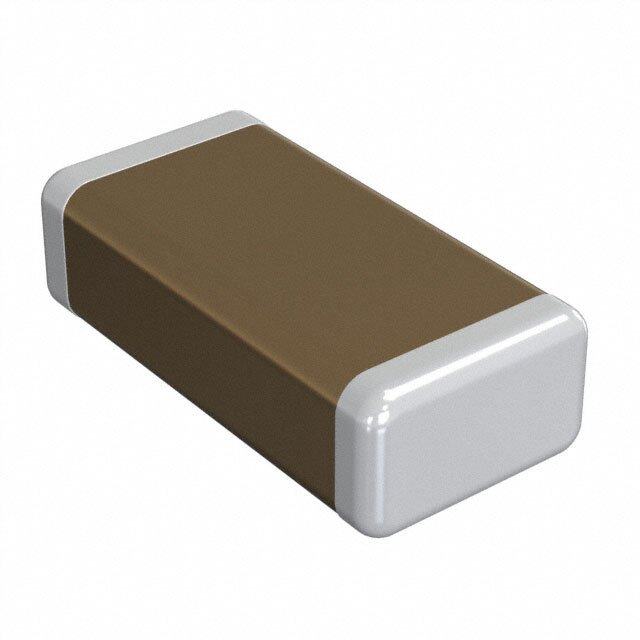
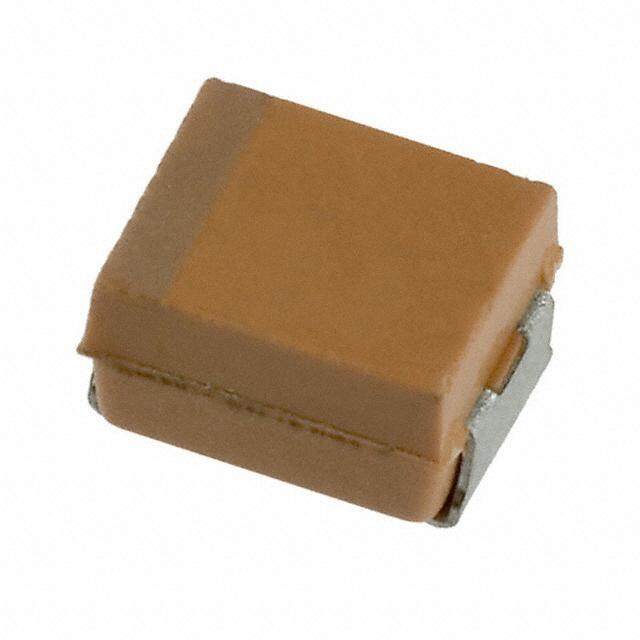
C0805T104K1RCLTU产品简介:
ICGOO电子元器件商城为您提供C0805T104K1RCLTU由Kemet设计生产,在icgoo商城现货销售,并且可以通过原厂、代理商等渠道进行代购。 提供C0805T104K1RCLTU价格参考¥2.17-¥5.71以及KemetC0805T104K1RCLTU封装/规格参数等产品信息。 你可以下载C0805T104K1RCLTU参考资料、Datasheet数据手册功能说明书, 资料中有C0805T104K1RCLTU详细功能的应用电路图电压和使用方法及教程。
| 参数 | 数值 |
| 产品目录 | |
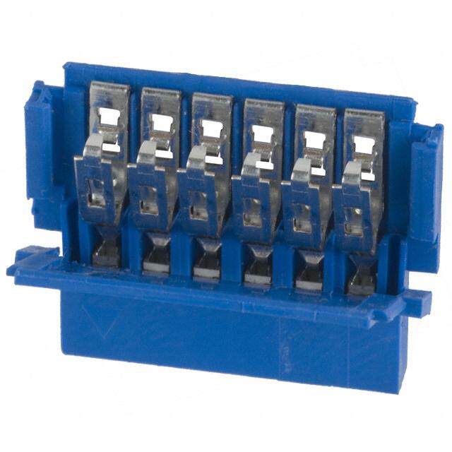
| 描述 | CAP CER 0.1UF 100V 10% X7R 0805 |
| 产品分类 | |
| 品牌 | Kemet |
| 数据手册 | |
| 产品图片 |
|
| 产品型号 | C0805T104K1RCLTU |
| rohs | 含铅 / 不符合限制有害物质指令(RoHS)规范要求 |
| 产品系列 | - |
| 产品培训模块 | http://www.digikey.cn/PTM/IndividualPTM.page?site=cn&lang=zhs&ptm=25569 |
| 其它名称 | 399-6310-1 |
| 包装 | 剪切带 (CT) |
| 厚度(最大值) | 0.043"(1.10mm) |
| 大小/尺寸 | 0.079" 长 x 0.049" 宽(2.00mm x 1.25mm) |
| 安装类型 | 表面贴装,MLCC |
| 容差 | ±10% |
| 封装/外壳 | 0805(2012 公制) |
| 工作温度 | -55°C ~ 125°C |
| 应用 | 高可靠性 |
| 引线形式 | - |
| 引线间距 | - |
| 标准包装 | 1 |
| 温度系数 | X7R |
| 特性 | - |
| 电压-额定 | 100V |
| 电容 | 0.1µF |
| 等级 | COTS |
| 高度-安装(最大值) | - |


- 商务部:美国ITC正式对集成电路等产品启动337调查
- 曝三星4nm工艺存在良率问题 高通将骁龙8 Gen1或转产台积电
- 太阳诱电将投资9.5亿元在常州建新厂生产MLCC 预计2023年完工
- 英特尔发布欧洲新工厂建设计划 深化IDM 2.0 战略
- 台积电先进制程称霸业界 有大客户加持明年业绩稳了
- 达到5530亿美元!SIA预计今年全球半导体销售额将创下新高
- 英特尔拟将自动驾驶子公司Mobileye上市 估值或超500亿美元
- 三星加码芯片和SET,合并消费电子和移动部门,撤换高东真等 CEO
- 三星电子宣布重大人事变动 还合并消费电子和移动部门
- 海关总署:前11个月进口集成电路产品价值2.52万亿元 增长14.8%

PDF Datasheet 数据手册内容提取
Surface Mount Multilayer Ceramic Chip Capacitors (SMD MLCCs) Commercial Off-The-Shelf (COTS) for Higher Reliability Applications, X7R Dielectric, 6.3 – 250 VDC Overview KEMET’s COTS program is an extension of KEMET knowledge All COTS testing includes voltage conditioning and post-electrical of high reliability test regimes and requirements. KEMET testing as per MIL–PRF–55681. For enhanced reliability, KEMET regularly supplies “up-screened” products by working with also provides the following test level options and conformance customer drawings and imposing specified design and test certifications: requirements. The COTS program offers the same high quality Test Level A Test Level B Test Level C and high reliability components as up-screened products, but at a lower cost to the customer. This is accomplished by Voltage Conditioning Voltage Conditioning Voltage Conditioning eliminating the need for customer-specific drawings to achieve DWV DWV DWV IR@25°C IR@25°C IR@25°C the reliability level required for customer applications. A series CAP CAP CAP DF DF DF of tests and inspections have been selected to provide the accelerated conditioning and 100% screening necessary to PDA 8% PDA 8% PDA 8% eliminate infant mortal failures from the population. C of C DPA DPA KEMET’s X7R dielectric features a 125°C maximum operating temperature and is considered “temperature stable.” The C of C 85/85 Electronics Components, Assemblies & Materials Association C of C (EIA) characterizes X7R dielectric as a Class II material. Components of this classification are fixed, ceramic dielectric capacitors suited for bypass and decoupling applications or for frequency discriminating circuits where Q and stability of capacitance characteristics are not critical. X7R exhibits a predictable change in capacitance with respect to time and voltage and boasts a minimal change in capacitance with reference to ambient temperature. Capacitance change is limited to ±15% from −55°C to +125°C. Ordering Information C 1210 T 104 K 5 R A C TU Rated Case Size Specification/ Capacitance Capacitance Termination Packaging/ Ceramic Voltage Dielectric Test Level (L" x W") Series Code (pF) Tolerance Finish1 Grade (C-Spec) (VDC) 0402 T = COTS Two J = ±5% 9 = 6.3 R = X7R A = Testing per MIL- C = 100% See 0603 significant K = ±10% 8 = 10 PRF-55681 PDA 8% Matte Sn "Packaging 0805 digits and M = ±20% 4 = 16 B= Testing per MIL- L = SnPb (5% C-Spec 1206 number of 3 = 25 PRF-55681 PDA 8%, DPA Pb minimum) Ordering 1210 zeros 5 = 50 per EIA-469 Options Table" 1812 1 = 100 C = Testing per MIL- 2220 2 = 200 PRF-55681 PDA 8%, DPA A = 250 per EIA-469, Humidity per MIL-STD-202, Method 103, Condition A 1 Additional termination finish options may be available. Contact KEMET for details. One world. One KEMET © KEMET Electronics Corporation • KEMET Tower • One East Broward Boulevard C1027_X7R_COTS_SMD • 6/12/2019 1 Fort Lauderdale, FL 33301 USA • 954-766-2800 • www.kemet.com
Surface Mount Multilayer Ceramic Chip Capacitors (SMD MLCCs) Commercial Off-The-Shelf (COTS) for Higher Reliability Applications, X7R Dielectric, 6.3 – 250 VDC Packaging C-Spec Ordering Options Table Packaging/Grade Packaging Type1 Ordering Code (C-Spec) Bulk Bag/Unmarked Not required (Blank) 7" Reel/Unmarked TU 7411 (EIA 0603 and smaller case sizes) 13" Reel/Unmarked 7210 (EIA 0805 and larger case sizes) 7" Reel/Marked TM 7040 (EIA 0603) 13" Reel/Marked 7215 (EIA 0805 and larger case sizes) 7" Reel/Unmarked/2mm pitch2 7081 13" Reel/Unmarked/2mm pitch2 7082 1 Default packaging is "Bulk Bag". An ordering code C-Spec is not required for "Bulk Bag" packaging. 1 The terms "Marked" and "Unmarked" pertain to laser marking option of capacitors. All packaging options labeled as "Unmarked" will contain capacitors that have not been laser marked. Please contact KEMET if you require a laser marked option. For more information see "Capacitor Marking". 2 The 2 mm pitch option allows for double the packaging quantity of capacitors on a given reel size. This option is limited to EIA 0603 (1608 metric) case size devices. For more information regarding 2 mm pitch option see "Tape & Reel Packaging Information". Benefits • −55°C to +125°C operating temperature range • DC voltage ratings of 6.3 V, 10 V, 16 V, 25 V, 50 V, 100 V, • Lead (Pb)-free, RoHS and REACH compliant 200 V, and 250 V • Voltage conditioning and post-electrical testing per • Capacitance offerings ranging from 10 pF to 22 μF MIL–PRF–55681 • Available capacitance tolerances of ±5%, ±10%, and ±20% • Destructive Physical Analysis (DPA) per EIA–469 • Non-polar device, minimizing installation concerns • Biased humidity testing (85/85) per MIL–STD–202 • 100% pure matte tin-plated termination finish allowing for • Certificate of Compliance excellent solderability • Temperature stable dielectric • SnPb termination finish option available upon request • EIA 0402, 0603, 0805, 1206, 1210, 1812, and (5% Pb minimum) 2220 case sizes Applications Typical applications include military, space quality and high reliability electronics. © KEMET Electronics Corporation • KEMET Tower • One East Broward Boulevard C1027_X7R_COTS_SMD • 6/12/2019 2 Fort Lauderdale, FL 33301 USA • 954-766-2800 • www.kemet.com
Surface Mount Multilayer Ceramic Chip Capacitors (SMD MLCCs) Commercial Off-The-Shelf (COTS) for Higher Reliability Applications, X7R Dielectric, 6.3 – 250 VDC Dimensions – Millimeters (Inches) W L T B S S EIA Size Metric Size L W T B Mounting Separation Code Code Length Width Thickness Bandwidth Technique Minimum 1.00 (0.040) 0.50 (0.020) 0.30 (0.012) Solder Reflow 0402 1005 0.30 (0.012) ±0.05 (0.002) ±0.05 (0.002) ±0.10 (0.004) Only 1.60 (0.063) 0.80 (0.032) 0.35 (0.014) 0603 1608 0.70 (0.028) ±0.15 (0.006) ±0.15 (0.006) ±0.15 (0.006) 2.00 (0.079) 1.25 (0.049) 0.50 (0.02) Solder Wave or 0805 2012 0.75 (0.030) ±0.20 (0.008) +0.20 (0.008) ±0.25 (0.010) Solder Reflow 3.20 (0.126) 1.60 (0.063) See Table 2 for 0.50 (0.02) 1206 3216 ±0.20 (0.008) ±0.20 (0.008) Thickness ±0.25 (0.010) 3.20 (0.126) 2.50 (0.098) 0.50 (0.02) 12101 3225 +0.20 (0.008) ±0.20 (0.008) ±0.25 (0.010) N/A 4.50 (0.177) 3.20 (0.126) 0.60 (0.024) Solder Reflow 1812 4532 ±0.30 (0.012) ±0.30 (0.012) ±0.35 (0.014) Only 5.70 (0.224) 5.00 (0.197) 0.60 (0.024) 2220 5650 ±0.40 (0.016) ±0.40 (0.016) ±0.35 (0.014) 1 For capacitance values ≥ 4.7 µF add 0.02 (0.001) to the width tolerance dimension and 0.10 (0.004) to the length tolerance dimension. Qualification/Certification Commercial Grade products are subject to internal qualification. Details regarding test methods and conditions are refer- enced in Table 4, Performance & Reliability. Environmental Compliance Lead (Pb)-free, RoHS, and REACH compliant without exemptions (excluding SnPb termination finish option). © KEMET Electronics Corporation • KEMET Tower • One East Broward Boulevard C1027_X7R_COTS_SMD • 6/12/2019 3 Fort Lauderdale, FL 33301 USA • 954-766-2800 • www.kemet.com
Surface Mount Multilayer Ceramic Chip Capacitors (SMD MLCCs) Commercial Off-The-Shelf (COTS) for Higher Reliability Applications, X7R Dielectric, 6.3 – 250 VDC Electrical Parameters/Characteristics Item Parameters/Characteristics Operating Temperature Range −55°C to +125°C Capacitance Change with Reference to ±15% +25°C and 0 Vdc Applied (TCC) 1Aging Rate (Maximum % Capacitance Loss/Decade Hour) 3.0% 250% of rated voltage 2Dielectric Withstanding Voltage (DWV) (5±1 seconds and charge/discharge not exceeding 50mA) 3Dissipation Factor (DF) Maximum Limit at 25°C 5%(6.3V & 10V), 3.5%(16V & 25V) and 2.5%(50V to 250V) See Insulation Resistance Limit Table 4Insulation Resistance (IR) Minimum Limit at 25°C (Rated voltage applied for 120±5 seconds at 25°C) 1 Regarding Aging Rate: Capacitance measurements (including tolerance) are indexed to a referee time of 1,000 hours. 2 DWV is the voltage a capacitor can withstand (survive) for a short period of time. It exceeds the nominal and continuous working voltage of the capacitor. 3 Capacitance and dissipation factor (DF) measured under the following conditions: 1kHz ± 50Hz and 1.0 ± 0.2 Vrms if capacitance ≤10µF 120Hz ± 10Hz and 0.5 ± 0.1 Vrms if capacitance >10µF 4 To obtain IR limit, divide MΩ-µF value by the capacitance and compare to GΩ limit. Select the lower of the two limits. Note: When measuring capacitance it is important to ensure the set voltage level is held constant. The HP4284 & Agilent E4980 have a feature known as Automatic Level Control (ALC). The ALC feature should be switched to "ON". Post Environmental Limits High Temperature Life, Biased Humidity, Moisture Resistance Rated DC Capacitance Dissipation Factor Capacitance Insulation Dielectric Voltage Value (Maximum %) Shift Resistance > 25 3.0 10% of Initial X7R 16/25 All 5.0 ±20% Limit < 16 7.5 Insulation Resistance Limit Table 1,000 Megohm 500 Megohm EIA Case Size Microfarads or 100 GΩ Microfarads or 10 GΩ 0201 N/A ALL 0402 < 0.012 µF ≥ 0.012 µF 0603 < 0.047 µF ≥ 0.047 µF 0805 < 0.15 µF ≥ 0.15 µF 1206 < 0.47 µF ≥ 0.47 µF 1210 < 0.39 µF ≥ 0.39 µF 1808 ALL N/A 1812 < 2.2 µF ≥ 2.2 µF 1825 ALL N/A 2220 < 10 µF ≥ 10 µF 2225 ALL N/A © KEMET Electronics Corporation • KEMET Tower • One East Broward Boulevard C1027_X7R_COTS_SMD • 6/12/2019 4 Fort Lauderdale, FL 33301 USA • 954-766-2800 • www.kemet.com
Surface Mount Multilayer Ceramic Chip Capacitors (SMD MLCCs) Commercial Off-The-Shelf (COTS) for Higher Reliability Applications, X7R Dielectric, 6.3 – 250 VDC Table 1A – Capacitance Range/Selection Waterfall (0402 – 1206 Case Sizes) Case Size/ C0402T C0603T C0805T C1206T Series Cap Capacitance Voltage Code 9 8 4 3 5 9 8 4 3 5 1 2 9 8 4 3 5 1 2 A 9 8 4 3 5 1 2 A Code Rate(dV VDoCl)tage 6.3 10 16 25 50 6.3 10 16 25 50 100 200 6.3 10 16 25 50 100 200 250 6.3 10 16 25 50 100 200 250 Capacitance Product Availability and Chip Thickness Codes Tolerance See Table 2 for Chip Thickness Dimensions 10 – 91 pF* 100 – 910* J K M BB BB BB BB BB CF CF CF CF CF CF CF DN DN DN DN DN DN DN EB EB EB EB EB EB EB 100 – 150 pF** 101 – 151** J K M BB BB BB BB BB CF CF CF CF CF CF CF DN DN DN DN DN DN DN EB EB EB EB EB EB EB 180 – 820 pF** 181 – 821** J K M BB BB BB BB BB CF CF CF CF CF CF CF DN DN DN DN DN DN DN DN EB EB EB EB EB EB EB 1,000 pF 102 J K M BB BB BB BB BB CF CF CF CF CF CF CF DN DN DN DN DN DN DN DN EB EB EB EB EB EB EB EB 1,200 pF 122 J K M BB BB BB BB BB CF CF CF CF CF CF CF DN DN DN DN DN DN DN DN EB EB EB EB EB EB EB EB 1,500 pF 152 J K M BB BB BB BB BB CF CF CF CF CF CF CF DN DN DN DN DN DN DN DN EB EB EB EB EB EB EB EB 1,800 pF 182 J K M BB BB BB BB BB CF CF CF CF CF CF CF DN DN DN DN DN DN DN DN EB EB EB EB EB EB EB EB 2,200 pF 222 J K M BB BB BB BB BB CF CF CF CF CF CF CF DN DN DN DN DN DN DN DN EB EB EB EB EB EB EB EB 2,700 pF 272 J K M BB BB BB BB BB CF CF CF CF CF CF CF DN DN DN DN DN DN DN DN EB EB EB EB EB EB EB EB 3,300 pF 332 J K M BB BB BB BB BB CF CF CF CF CF CF CF DN DN DN DN DN DN DN DN EB EB EB EB EB EB EB EB 3,900 pF 392 J K M BB BB BB BB BB CF CF CF CF CF CF CF DN DN DN DN DN DN DN DN EB EB EB EB EB EB EB EB 4,700 pF 472 J K M BB BB BB BB BB CF CF CF CF CF CF CF DN DN DN DN DN DN DN DN EB EB EB EB EB EB EB EB 5,600 pF 562 J K M BB BB BB BB BB CF CF CF CF CF CF CF DN DN DN DN DN DN DN DN EB EB EB EB EB EB EB EB 6,800 pF 682 J K M BB BB BB BB BB CF CF CF CF CF CF CF DN DN DN DN DN DN DN DN EB EB EB EB EB EB EB EB 8,200 pF 822 J K M BB BB BB BB BB CF CF CF CF CF CF CF DN DN DN DN DN DN DN DN EB EB EB EB EB EB EB EB 10,000 pF 103 J K M BB BB BB BB BB CF CF CF CF CF CF CF DN DN DN DN DN DN DN DN EB EB EB EB EB EB EB EB 12,000 pF 123 J K M BB BB BB BB BB CF CF CF CF CF CF DN DN DN DN DN DN DN DN EB EB EB EB EB EB EB EB 15,000 pF 153 J K M BB BB BB BB BB CF CF CF CF CF CF DN DN DN DN DN DP DN DN EB EB EB EB EB EB EB EB 18,000 pF 183 J K M BB BB BB BB BB CF CF CF CF CF CF DN DN DN DN DN DP DN DN EB EB EB EB EB EB EB EB 22,000 pF 223 J K M BB BB BB BB BB CF CF CF CF CF CF DN DN DN DN DN DP DN DN EB EB EB EB EB EB EB EB 27,000 pF 273 J K M BB BB BB BB CF CF CF CF CF CF DN DN DN DN DN DP DE EB EB EB EB EB EB EB EB 33,000 pF 333 J K M BB BB BB BB CF CF CF CF CF CF DN DN DN DN DN DP DE EB EB EB EB EB EB EB EB 39,000 pF 393 J K M BB BB BB BB CF CF CF CF CF CF DN DN DN DN DN DP DE EB EB EB EB EB EC EB EB 47,000 pF 473 J K M BB BB BB BB CF CF CF CF CF CF DN DN DN DN DN DE DG EB EB EB EB EB EC ED ED 56,000 pF 563 J K M BB BB BB CF CF CF CF CF DP DP DP DP DP DE DG EB EB EB EB EB EB ED ED 68,000 pF 683 J K M BB BB BB CF CF CF CF CF DP DP DP DP DP DE EB EB EB EB EB EB ED ED 82,000 pF 823 J K M BB BB BB CF CF CF CF CF DP DP DP DP DP DE EB EB EB EB EB EB ED ED 0.10 µF 104 J K M BB BB BB CF CF CF CF CF DN DN DN DN DN DE EB EB EB EB EB EB EM EM 0.12 µF 124 J K M CF CF CF CF CF DN DN DN DN DP DG EC EC EC EC EC EC EG 0.15 µF 154 J K M CF CF CF CF CF DN DN DN DN DP DG EC EC EC EC EC EC EG 0.18 µF 184 J K M CF CF CF CF DN DN DN DN DP DG EC EC EC EC EC EC 0.22 µF 224 J K M CF CF CF CF DN DN DN DN DP DG EC EC EC EC EC EC 0.27 µF 274 J K M CF CF CF DP DP DP DP DP EB EB EB EB EC EM 0.33 µF 334 J K M CF CF CF DP DP DP DP DP EB EB EB EB EC EG 0.39 µF 394 J K M CF CF CF DG DG DG DG DE EB EB EB EB EC EG 0.47 µF 474 J K M CF CF CF DP DP DP DP DE EC EC EC EC EC EG 0.56 µF 564 J K M DP DP DP DG DH ED ED ED ED EC 0.68 µF 684 J K M DP DP DP DG DH EE EE EE EE ED 0.82 µF 824 J K M DP DP DP DG EF EF EF EF ED 1.0 µF 105 J K M DP DP DP DG EF EF EF EG ED 1.2 µF 125 J K M DE DE DE ED ED ED EG EH 1.5 µF 155 J K M DG DG DG EF EF EF EG EH 1.8 µF 185 J K M DG DG DG ED ED ED EF EH 2.2 µF 225 J K M DG DG DG ED ED ED EF EH 2.7 µF 275 J K M EN EN EN EH 3.3 µF 335 J K M ED ED ED EH 3.9 µF 395 J K M EF EF EF EH 4.7 µF 475 J K M EF EF EF EH 5.6 µF 565 J K M EH EH EH 6.8 µF 685 J K M EH EH EH Rate(dV VDoCl)tage 6.3 10 16 25 50 6.3 10 16 25 50 100 200 6.3 10 16 25 50 100 200 250 6.3 10 16 25 50 100 200 250 Cap Capacitance Code Voltage Code 9 8 4 3 5 9 8 4 3 5 1 2 9 8 4 3 5 1 2 A 9 8 4 3 5 1 2 A Case Size/ C0402T C0603T C0805T C1206T Series *Capacitance range Includes E24 decade values only. (i.e., 10, 11, 12, 13, 15, 16, 18, 20, 22, 24, 27, 30, 33, 36, 39, 43, 47, 51, 56, 62, 68, 75, 82, and 91) **Capacitance range Includes E12 decade values only. (i.e., 10, 12, 15, 18, 22, 27, 33, 39, 47, 56, 68, and 82) © KEMET Electronics Corporation • KEMET Tower • One East Broward Boulevard C1027_X7R_COTS_SMD • 6/12/2019 5 Fort Lauderdale, FL 33301 USA • 954-766-2800 • www.kemet.com
Surface Mount Multilayer Ceramic Chip Capacitors (SMD MLCCs) Commercial Off-The-Shelf (COTS) for Higher Reliability Applications, X7R Dielectric, 6.3 – 250 VDC Table 1A – Capacitance Range/Selection Waterfall (0402 – 1206 Case Sizes) cont'd Case Size/ C0402T C0603T C0805T C1206T Series Cap Capacitance Voltage Code 9 8 4 3 5 9 8 4 3 5 1 2 9 8 4 3 5 1 2 A 9 8 4 3 5 1 2 A Code Rate(dV VDoCl)tage 6.3 10 16 25 50 6.3 10 16 25 50 100 200 6.3 10 16 25 50 100 200 250 6.3 10 16 25 50 100 200 250 Capacitance Product Availability and Chip Thickness Codes Tolerance See Table 2 for Chip Thickness Dimensions 8.2 µF 825 J K M EH EH EH 10 µF 106 J K M EH EH EH Rate(dV VDoCl)tage 6.3 10 16 25 50 6.3 10 16 25 50 100 200 6.3 10 16 25 50 100 200 250 6.3 10 16 25 50 100 200 250 Cap Capacitance Code Voltage Code 9 8 4 3 5 9 8 4 3 5 1 2 9 8 4 3 5 1 2 A 9 8 4 3 5 1 2 A Case Size/ C0402T C0603T C0805T C1206T Series *Capacitance range Includes E24 decade values only. (i.e., 10, 11, 12, 13, 15, 16, 18, 20, 22, 24, 27, 30, 33, 36, 39, 43, 47, 51, 56, 62, 68, 75, 82, and 91) **Capacitance range Includes E12 decade values only. (i.e., 10, 12, 15, 18, 22, 27, 33, 39, 47, 56, 68, and 82) Table 1B – Capacitance Range/Selection Waterfall (1210 – 2220 Case Sizes) Case Size/ C1210T C1808T C1812T C1825T C2220T Series Cap Voltage Code 9 8 4 3 5 1 2 A 5 1 2 3 5 1 2 A 5 1 2 A 3 5 1 2 A Capacitance Code Rate(dV VDoCl)tage 6.3 10 16 25 50 100 200 250 50 100 200 25 50 100 200 250 50 100 200 250 25 50 100 200 250 Capacitance Product Availability and Chip Thickness Codes Tolerance See Table 2 for Chip Thickness Dimensions 10 - 91 pF* 100 - 910* J K M FB FB FB FB FB FB FB 100 - 270 pF** 101 - 391** J K M FB FB FB FB FB FB FB 330 pF 331 J K M FB FB FB FB FB FB FB LF LF LF 390 pF 391 J K M FB FB FB FB FB FB FB LF LF LF 470 - 820 pF** 471 - 821** J K M FB FB FB FB FB FB FB LF LF LF GB GB GB GB 1,000 pF 102 J K M FB FB FB FB FB FB FB LF LF LF GB GB GB GB 1,200 pF 122 J K M FB FB FB FB FB FB FB LF LF LF GB GB GB GB 1,500 pF 152 J K M FB FB FB FB FB FB FE LF LF LF GB GB GB GB 1,800 pF 182 J K M FB FB FB FB FB FB FE LF LF LF GB GB GB GB 2,200 pF 222 J K M FB FB FB FB FB FB FB FB LF LF LF GB GB GB GB 2,700 pF 272 J K M FB FB FB FB FB FB FB FB LF LF LF GB GB GB GB 3,300 pF 332 J K M FB FB FB FB FB FB FB FB LF LF GB GB GB GB 3,900 pF 392 J K M FB FB FB FB FB FB FB FB LF LF GB GB GB GB 4,700 pF 472 J K M FB FB FB FB FB FB FB FB LD LD GB GB GB GD 5,600 pF 562 J K M FB FB FB FB FB FB FB FB LD LD GB GB GB GH 6,800 pF 682 J K M FB FB FB FB FB FB FB FB LD LD GB GB GB GB GB JE JE JE 8,200 pF 822 J K M FB FB FB FB FB FB FB FB LD LD GB GB GB GB GB JE JE JE 10,000 pF 103 J K M FB FB FB FB FB FB FB FB LD LD GB GB GB GB GB JE JE JE 12,000 pF 123 J K M FB FB FB FB FB FB FB FB LD LD GB GB GB GB GB JE JE JE 15,000 pF 153 J K M FB FB FB FB FB FB FB FB LD LD GB GB GB GB GB JE JE JE 18,000 pF 183 J K M FB FB FB FB FB FB FB FB LD LD GB GB GB GB GB JE JE JE 22,000 pF 223 J K M FB FB FB FB FB FB FB FB LD LD GB GB GB GB GB HB HB HB HB JE JE JE 27,000 pF 273 J K M FB FB FB FB FB FB FB FB LD LD GB GB GB GB GB HB HB HB HB JE JE JE Rate(dV VDoCl)tage 6.3 10 16 25 50 100 200 250 50 100 200 25 50 100 200 250 50 100 200 250 25 50 100 200 250 Cap Capacitance Voltage Code 9 8 4 3 5 1 2 A 5 1 2 3 5 1 2 A 5 1 2 A 3 5 1 2 A Code Case Size/ C1210T C1808T C1812T C1825T C2220T Series *Capacitance range Includes E24 decade values only. (i.e., 10, 11, 12, 13, 15, 16, 18, 20, 22, 24, 27, 30, 33, 36, 39, 43, 47, 51, 56, 62, 68, 75, 82, and 91) **Capacitance range Includes E12 decade values only. (i.e., 10, 12, 15, 18, 22, 27, 33, 39, 47, 56, 68, and 82) © KEMET Electronics Corporation • KEMET Tower • One East Broward Boulevard C1027_X7R_COTS_SMD • 6/12/2019 6 Fort Lauderdale, FL 33301 USA • 954-766-2800 • www.kemet.com
Surface Mount Multilayer Ceramic Chip Capacitors (SMD MLCCs) Commercial Off-The-Shelf (COTS) for Higher Reliability Applications, X7R Dielectric, 6.3 – 250 VDC Table 1B – Capacitance Range/Selection Waterfall (1210 – 2220 Case Sizes) cont'd Case Size/ C1210T C1808T C1812T C1825T C2220T Series Cap Voltage Code 9 8 4 3 5 1 2 A 5 1 2 3 5 1 2 A 5 1 2 A 3 5 1 2 A Capacitance Code Rate(dV VDoCl)tage 6.3 10 16 25 50 100 200 250 50 100 200 25 50 100 200 250 50 100 200 250 25 50 100 200 250 Capacitance Product Availability and Chip Thickness Codes Tolerance See Table 2 for Chip Thickness Dimensions 33,000 pF 333 J K M FB FB FB FB FB FB FB FB LD LD GB GB GB GB GB HB HB HB HB JB JB JB 39,000 pF 393 J K M FB FB FB FB FB FB FB FB LD LD GB GB GB GB GB HB HB HB HB JB JB JB 47,000 pF 473 J K M FB FB FB FB FB FB FB FB LD LD GB GB GB GB GB HB HB HB HB JB JB JB 56,000 pF 563 J K M FB FB FB FB FB FB FC FC LD LD GB GB GB GB GB HB HB HB HB JB JB JB 68,000 pF 683 J K M FB FB FB FB FB FB FC FC LD GB GB GB GB GB HB HB HB HB JB JB JB 82,000 pF 823 J K M FB FB FB FB FB FC FF FF LD GB GB GB GB GB HB HB HB HB JB JB JC JC JC 0.10 µF 104 J K M FB FB FB FB FB FD FG FG LD GB GB GB GB GB HB HB HB HB JB JB JC JC JC 0.12 µF 124 J K M FB FB FB FB FB FD FH FH LD GB GB GB GB GB HB HB HB HB JB JB JC JC JC 0.15 µF 154 J K M FC FC FC FC FC FD FM FM LD GB GB GB GE GE HB HB HB HB JB JB JC JC JC 0.18 µF 184 J K M FC FC FC FC FC FD FK FK LD GB GB GB GG GG HB HB HB HB JB JB JC JC JC 0.22 µF 224 J K M FC FC FC FC FC FD FK FK GB GB GB GG GG HB HB HB HB JB JB JC JC JC 0.27 µF 274 J K M FC FC FC FC FC FD GB GB GG GG GG HB HB HB HB JC JC JC JC JC 0.33 µF 334 J K M FD FD FD FD FD FD GB GB GG GG GG HB HB HB HB JC JC JC JC JC 0.39 µF 394 J K M FD FD FD FD FD FD GB GB GG GG GG HD HD HD HD JC JC JC JC JC 0.47 µF 474 J K M FD FD FD FD FD FD GB GB GG GJ GJ HD HD HD HD JC JC JC JC JC 0.56 µF 564 J K M FD FD FD FD FD FF GC GC GG HD HD HD HD JC JD JD JD JD 0.68 µF 684 J K M FD FD FD FD FD FG GC GC GG HD HD HD HD JC JD JD JD JD 0.82 µF 824 J K M FF FF FF FF FF FL GE GE GG HF HF HF HF JC JF JF JF JF 1.0 µF 105 J K M FH FH FH FH FH FM GE GE GG HF HF HF HF JC JF JF JF JF 1.2 µF 125 J K M FH FH FH FH FG JC JC 1.5 µF 155 J K M FH FH FH FH FG JC JC 1.8 µF 185 J K M FH FH FH FH FG JD JD 2.2 µF 225 J K M FJ FJ FJ FJ FG GO GO JF JF 2.7 µF 275 J K M FE FE FE FG FH 3.3 µF 335 J K M FF FF FF FM FM 3.9 µF 395 J K M FG FG FG FG FK GK GK 4.7 µF 475 J K M FC FC FC FG FS GK GK JF JF 5.6 µF 565 J K M FF FF FF FH 6.8 µF 685 J K M FG FG FG FM 8.2 µF 825 J K M FH FH FH FK 10 µF 106 J K M FH FH FH FS GK JF JO 12 µF 126 J K M 15 µF 156 J K M JO 18 µF 186 J K M 22 µF 226 J K M FS FS JO Rate(dV VDoCl)tage 6.3 10 16 25 50 100 200 250 50 100 200 25 50 100 200 250 50 100 200 250 25 50 100 200 250 Cap Capacitance Voltage Code 9 8 4 3 5 1 2 A 5 1 2 3 5 1 2 A 5 1 2 A 3 5 1 2 A Code Case Size/ C1210T C1808T C1812T C1825T C2220T Series *Capacitance range Includes E24 decade values only. (i.e., 10, 11, 12, 13, 15, 16, 18, 20, 22, 24, 27, 30, 33, 36, 39, 43, 47, 51, 56, 62, 68, 75, 82, and 91) **Capacitance range Includes E12 decade values only. (i.e., 10, 12, 15, 18, 22, 27, 33, 39, 47, 56, 68, and 82) © KEMET Electronics Corporation • KEMET Tower • One East Broward Boulevard C1027_X7R_COTS_SMD • 6/12/2019 7 Fort Lauderdale, FL 33301 USA • 954-766-2800 • www.kemet.com
Surface Mount Multilayer Ceramic Chip Capacitors (SMD MLCCs) Commercial Off-The-Shelf (COTS) for Higher Reliability Applications, X7R Dielectric, 6.3 – 250 VDC Table 2A – Chip Thickness/Tape & Reel Packaging Quantities Thickness Case Thickness ± Paper Quantity1 Plastic Quantity Code Size1 Range (mm) 7" Reel 13" Reel 7" Reel 13" Reel BB 0402 0.50 ± 0.05 10,000 50,000 0 0 CF 0603 0.80 ± 0.07 4,000 15,000 0 0 DN 0805 0.78 ± 0.10 4,000 15,000 0 0 DP 0805 0.90 ± 0.10 4,000 15,000 0 0 DE 0805 1.00 ± 0.10 0 0 2,500 10,000 DG 0805 1.25 ± 0.15 0 0 2,500 10,000 DH 0805 1.25 ± 0.20 0 0 2,500 10,000 EB 1206 0.78 ± 0.10 4,000 10,000 4,000 10,000 EC 1206 0.90 ± 0.10 0 0 4,000 10,000 EN 1206 0.95 ± 0.10 0 0 4,000 10,000 ED 1206 1.00 ± 0.10 0 0 2,500 10,000 EE 1206 1.10 ± 0.10 0 0 2,500 10,000 EF 1206 1.20 ± 0.15 0 0 2,500 10,000 EM 1206 1.25 ± 0.15 0 0 2,500 10,000 EG 1206 1.60 ± 0.15 0 0 2,000 8,000 EH 1206 1.60 ± 0.20 0 0 2,000 8,000 FB 1210 0.78 ± 0.10 0 0 4,000 10,000 FC 1210 0.90 ± 0.10 0 0 4,000 10,000 FD 1210 0.95 ± 0.10 0 0 4,000 10,000 FE 1210 1.00 ± 0.10 0 0 2,500 10,000 FF 1210 1.10 ± 0.10 0 0 2,500 10,000 FG 1210 1.25 ± 0.15 0 0 2,500 10,000 FL 1210 1.40 ± 0.15 0 0 2,000 8,000 FH 1210 1.55 ± 0.15 0 0 2,000 8,000 FM 1210 1.70 ± 0.20 0 0 2,000 8,000 FJ 1210 1.85 ± 0.20 0 0 2,000 8,000 FK 1210 2.10 ± 0.20 0 0 2,000 8,000 FS 1210 2.50 ± 0.30 0 0 1,000 4,000 LD 1808 0.90 ± 0.10 0 0 2,500 10,000 LF 1808 1.00 ± 0.15 0 0 2,500 10,000 GB 1812 1.00 ± 0.10 0 0 1,000 4,000 GC 1812 1.10 ± 0.10 0 0 1,000 4,000 GD 1812 1.25 ± 0.15 0 0 1,000 4,000 GE 1812 1.30 ± 0.10 0 0 1,000 4,000 GH 1812 1.40 ± 0.15 0 0 1,000 4,000 GG 1812 1.55 ± 0.10 0 0 1,000 4,000 GK 1812 1.60 ± 0.20 0 0 1,000 4,000 GJ 1812 1.70 ± 0.15 0 0 1,000 4,000 GO 1812 2.50 ± 0.20 0 0 500 2,000 HB 1825 1.10 ± 0.15 0 0 1,000 4,000 HD 1825 1.30 ± 0.15 0 0 1,000 4,000 HF 1825 1.50 ± 0.15 0 0 1,000 4,000 JB 2220 1.00 ± 0.15 0 0 1,000 4,000 JC 2220 1.10 ± 0.15 0 0 1,000 4,000 JD 2220 1.30 ± 0.15 0 0 1,000 4,000 JE 2220 1.40 ± 0.15 0 0 1,000 4,000 JF 2220 1.50 ± 0.15 0 0 1,000 4,000 JO 2220 2.40 ± 0.15 0 0 500 2,000 7" Reel 13" Reel 7" Reel 13" Reel Thickness Case Thickness ± Code Size1 Range (mm) Paper Quantity1 Plastic Quantity Package quantity based on finished chip thickness specifications. 1 If ordering using the 2 mm Tape and Reel pitch option, the packaging quantity outlined in the table above will be doubled. This option is limited to EIA 0603 (1608 metric) case size devices. For more information regarding 2 mm pitch option see “Tape & Reel Packaging Information”. © KEMET Electronics Corporation • KEMET Tower • One East Broward Boulevard C1027_X7R_COTS_SMD • 6/12/2019 8 Fort Lauderdale, FL 33301 USA • 954-766-2800 • www.kemet.com
Surface Mount Multilayer Ceramic Chip Capacitors (SMD MLCCs) Commercial Off-The-Shelf (COTS) for Higher Reliability Applications, X7R Dielectric, 6.3 – 250 VDC Table 2B – Bulk Packaging Quantities Loose Packaging Packaging Type Bulk Bag (default) Packaging C-Spec1 N/A2 Case Size Packaging Quantities (pieces/unit packaging) EIA (in) Metric (mm) Minimum Maximum 0402 1005 0603 1608 0805 2012 50,000 1206 3216 1210 3225 1 1808 4520 1812 4532 1825 4564 20,000 2220 5650 2225 5664 1 The "Packaging C-Spec" is a 4 to 8 digit code which identifies the packaging type and/or product grade. When ordering, the proper code must be included in the 15th through 22nd character positions of the ordering code. See "Ordering Information" section of this document for further details. Commercial Grade product ordered without a packaging C-Spec will default to our standard "Bulk Bag" packaging. Contact KEMET if you require a bulk bag packaging option for Automotive Grade products. 2 A packaging C-Spec (see note 1 above) is not required for "Bulk Bag" packaging (excluding Anti-Static Bulk Bag and Automotive Grade products). The 15th through 22nd character positions of the ordering code should be left blank. All product ordered without a packaging C-Spec will default to our standard "Bulk Bag" packaging. © KEMET Electronics Corporation • KEMET Tower • One East Broward Boulevard C1027_X7R_COTS_SMD • 6/12/2019 9 Fort Lauderdale, FL 33301 USA • 954-766-2800 • www.kemet.com
Surface Mount Multilayer Ceramic Chip Capacitors (SMD MLCCs) Commercial Off-The-Shelf (COTS) for Higher Reliability Applications, X7R Dielectric, 6.3 – 250 VDC Table 3 – Chip Capacitor Land Pattern Design Recommendations per IPC–7351 Density Level A: Density Level B: Density Level C: EIA Metric Maximum (Most) Median (Nominal) Minimum (Least) Size Size Land Protrusion (mm) Land Protrusion (mm) Land Protrusion (mm) Code Code C Y X V1 V2 C Y X V1 V2 C Y X V1 V2 0402 1005 0.50 0.72 0.72 2.20 1.20 0.45 0.62 0.62 1.90 1.00 0.40 0.52 0.52 1.60 0.80 0603 1608 0.90 1.15 1.10 4.00 2.10 0.80 0.95 1.00 3.10 1.50 0.60 0.75 0.90 2.40 1.20 0805 2012 1.00 1.35 1.55 4.40 2.60 0.90 1.15 1.45 3.50 2.00 0.75 0.95 1.35 2.80 1.70 1206 3216 1.60 1.35 1.90 5.60 2.90 1.50 1.15 1.80 4.70 2.30 1.40 0.95 1.70 4.00 2.00 1210 3225 1.60 1.35 2.80 5.65 3.80 1.50 1.15 2.70 4.70 3.20 1.40 0.95 2.60 4.00 2.90 12101 3225 1.50 1.60 2.90 5.60 3.90 1.40 1.40 2.80 4.70 3.30 1.30 1.20 2.70 4.00 3.00 1812 4532 2.15 1.60 3.60 6.90 4.60 2.05 1.40 3.50 6.00 4.00 1.95 1.20 3.40 5.30 3.70 2220 5650 2.75 1.70 5.50 8.20 6.50 2.65 1.50 5.40 7.30 5.90 2.55 1.30 5.30 6.60 5.60 1 Only for capacitance values ≥ 22 µF Density Level A: For low-density product applications. Recommended for wave solder applications and provides a wider process window for reflow solder processes. KEMET only recommends wave soldering of EIA 0603, 0805, and 1206 case sizes. Density Level B: For products with a moderate level of component density. Provides a robust solder attachment condition for reflow solder processes. Density Level C: For high component density product applications. Before adapting the minimum land pattern variations the user should perform qualification testing based on the conditions outlined in IPC Standard 7351 (IPC–7351). Image below based on Density Level B for an EIA 1210 case size. V1 Y Y X X V2 C C Grid Placement Courtyard © KEMET Electronics Corporation • KEMET Tower • One East Broward Boulevard C1027_X7R_COTS_SMD • 6/12/2019 10 Fort Lauderdale, FL 33301 USA • 954-766-2800 • www.kemet.com
Surface Mount Multilayer Ceramic Chip Capacitors (SMD MLCCs) Commercial Off-The-Shelf (COTS) for Higher Reliability Applications, X7R Dielectric, 6.3 – 250 VDC Soldering Process Recommended Soldering Technique: • Solder wave or solder reflow for EIA case sizes 0603, 0805 and 1206 • All other EIA case sizes are limited to solder reflow only Recommended Reflow Soldering Profile: KEMET’s families of surface mount multilayer ceramic capacitors (SMD MLCCs) are compatible with wave (single or dual), convection, IR or vapor phase reflow techniques. Preheating of these components is recommended to avoid extreme thermal stress. KEMET’s recommended profile conditions for convection and IR reflow reflect the profile conditions of the IPC/J- STD-020 standard for moisture sensitivity testing. These devices can safely withstand a maximum of three reflow passes at these conditions. Termination Finish T Profile Feature P Maximum Ramp-up Rate = 3°C/second tP SnPb 100% Matte Sn Maximum Ramp-down Rate = 6°C/second T Preheat/Soak e L tL r Temperature Minimum (TSmin) 100°C 150°C ratu Tsmax Temperature Maximum (T ) 150°C 200°C e Smax mp T Time (t) from T to T 60 – 120 seconds 60 – 120 seconds e smin t S Smin Smax T s 3°C/second 3°C/second Ramp-Up Rate (T to T ) L P maximum maximum 25 25°C to Peak Liquidous Temperature (T) 183°C 217°C L Time Time Above Liquidous (t) 60 – 150 seconds 60 – 150 seconds L Peak Temperature (T ) 235°C 260°C P Time Within 5°C of Maximum 20 seconds 30 seconds Peak Temperature (t ) maximum maximum P 6°C/second 6°C/second Ramp-Down Rate (T to T) P L maximum maximum Time 25°C to Peak 6 minutes 8 minutes Temperature maximum maximum Note 1: All temperatures refer to the center of the package, measured on the capacitor body surface that is facing up during assembly reflow. © KEMET Electronics Corporation • KEMET Tower • One East Broward Boulevard C1027_X7R_COTS_SMD • 6/12/2019 11 Fort Lauderdale, FL 33301 USA • 954-766-2800 • www.kemet.com
Surface Mount Multilayer Ceramic Chip Capacitors (SMD MLCCs) Commercial Off-The-Shelf (COTS) for Higher Reliability Applications, X7R Dielectric, 6.3 – 250 VDC Table 4 – Performance & Reliability: Test Methods and Conditions Stress Reference Test or Inspection Method Terminal Strength JIS–C–6429 Appendix 1, Note: Force of 1.8 kg for 60 seconds. Appendix 2, Note: Standard termination system – 2.0 mm (minimum) for all except 3 mm Board Flex JIS–C–6429 for C0G. Flexible termination system – 3.0 mm (minimum). Magnification 50 X. Conditions: a) Method B, 4 hours at 155°C, dry heat at 235°C Solderability J–STD–002 b) Method B at 215°C category 3 c) Method D, category 3 at 260°C Temperature Cycling JESD22 Method JA–104 1,000 Cycles (−55°C to +125°C). Measurement at 24 hours +/−4 hours after test conclusion. Load Humidity: 1,000 hours 85°C/85% RH and rated voltage. Add 100 K ohm resistor. MIL–STD–202 Method Measurement at 24 hours +/−4 hours after test conclusion. Biased Humidity 103 Low Volt Humidity: 1,000 hours 85°C/85% RH and 1.5 V. Add 100 K ohm resistor. Measurement at 24 hours +/−4 hours after test conclusion. MIL–STD–202 Method t = 24 hours/cycle. Steps 7a and 7b not required. Moisture Resistance 106 Measurement at 24 hours +/−4 hours after test conclusion. MIL–STD–202 Method −55°C/+125°C. Note: Number of cycles required – 300, maximum transfer time – 20 Thermal Shock 107 seconds, dwell time – 15 minutes. Air – Air. MIL–STD–202 Method High Temperature Life 108 1,000 hours at 125°C (85°C for X5R, Z5U and Y5V) with 2 X rated voltage applied. /EIA–198 MIL–STD–202 Method Storage Life 150°C, 0 VDC for 1,000 hours. 108 5 g's for 20 min., 12 cycles each of 3 orientations. Note: Use 8" X 5" PCB 0.031" thick 7 MIL–STD–202 Method Vibration secure points on one long side and 2 secure points at corners of opposite sides. Parts 204 mounted within 2" from any secure point. Test from 10 – 2,000 Hz MIL–STD–202 Method Mechanical Shock Figure 1 of Method 213, Condition F. 213 MIL–STD–202 Method Resistance to Solvents Add aqueous wash chemical, OKEM Clean or equivalent. 215 Storage & Handling Ceramic chip capacitors should be stored in normal working environments. While the chips themselves are quite robust in other environments, solderability will be degraded by exposure to high temperatures, high humidity, corrosive atmospheres, and long term storage. In addition, packaging materials will be degraded by high temperature–reels may soften or warp and tape peel force may increase. KEMET recommends that maximum storage temperature not exceed 40ºC and maximum storage humidity not exceed 70% relative humidity. Temperature fluctuations should be minimized to avoid condensation on the parts and atmospheres should be free of chlorine and sulfur bearing compounds. For optimized solderability chip stock should be used promptly, preferably within 1.5 years of receipt. © KEMET Electronics Corporation • KEMET Tower • One East Broward Boulevard C1027_X7R_COTS_SMD • 6/12/2019 12 Fort Lauderdale, FL 33301 USA • 954-766-2800 • www.kemet.com
Surface Mount Multilayer Ceramic Chip Capacitors (SMD MLCCs) Commercial Off-The-Shelf (COTS) for Higher Reliability Applications, X7R Dielectric, 6.3 – 250 VDC Construction Detailed Cross Section Dielectric Material (BaTiO) 3 Barrier Layer Dielectric Termination Finish (Ni) Material (BaTiO3) (100% Matte Sn / SnPb - 5% Pb min) End Termination/ External Electrode (Cu) Inner Electrodes (Ni) End Termination/ External Electrode (Cu) Barrier Layer (Ni) Termination Finish (100% Matte Sn / SnPb - 5% Pb min) Inner Electrodes (Ni) © KEMET Electronics Corporation • KEMET Tower • One East Broward Boulevard C1027_X7R_COTS_SMD • 6/12/2019 13 Fort Lauderdale, FL 33301 USA • 954-766-2800 • www.kemet.com
Surface Mount Multilayer Ceramic Chip Capacitors (SMD MLCCs) Commercial Off-The-Shelf (COTS) for Higher Reliability Applications, X7R Dielectric, 6.3 – 250 VDC Capacitor Marking (Optional): These surface mount multilayer ceramic capacitors are Marking appears in legible contrast. Illustrated below normally supplied unmarked. If required, they can be is an example of an MLCC with laser marking of “KA8”, marked as an extra cost option. Marking is available which designates a KEMET device with rated capacitance on most KEMET devices, but must be requested using of 100 µF. Orientation of marking is vendor optional. the correct ordering code identifi er(s). If this option is requested, two sides of the ceramic body will be laser marked with a “K” to identify KEMET, followed by two characters (per EIA–198 - see table below) to identify the capacitance value. EIA 0603 case size devices are limited 2-Digit KEMET to the “K” character only. Capacitance ID Code Laser marking option is not available on: • C0G, ultra stable X8R and Y5V dielectric devices. • EIA 0402 case size devices. • EIA 0603 case size devices with fl exible termination option. • KPS commercial and automotive grade stacked devices. • X7R dielectric products in capacitance values outlined below. EIA Case Size Metric Size Code Capacitance 0603 1608 ≤ 170 pF 0805 2012 ≤ 150 pF 1206 3216 ≤ 910 pF 1210 3225 ≤ 2,000 pF 1808 4520 ≤ 3,900 pF 1812 4532 ≤ 6,700 pF 1825 4564 ≤ 0.018 µF 2220 5650 ≤ 0.027 µF 2225 5664 ≤ 0.033 µF © KEMET Electronics Corporation • KEMET Tower • One East Broward Boulevard C1027_X7R_COTS_SMD • 6/12/2019 14 Fort Lauderdale, FL 33301 USA • 954-766-2800 • www.kemet.com
Surface Mount Multilayer Ceramic Chip Capacitors (SMD MLCCs) Commercial Off-The-Shelf (COTS) for Higher Reliability Applications, X7R Dielectric, 6.3 – 250 VDC Capacitor Marking (Optional) cont’d Capacitance (pF) For Various Alpha/Numeral Identifi ers Numeral Alpha 9 0 1 2 3 4 5 6 7 8 Character Capacitance (pF) A 0.10 1.0 10 100 1,000 10,000 100,000 1,000,000 10,000,000 100,000,000 B 0.11 1.1 11 110 1,100 11,000 110,000 1,100,000 11,000,000 110,000,000 C 0.12 1.2 12 120 1,200 12,000 120,000 1,200,000 12,000,000 120,000,000 D 0.13 1.3 13 130 1,300 13,000 130,000 1,300,000 13,000,000 130,000,000 E 0.15 1.5 15 150 1,500 15,000 150,000 1,500,000 15,000,000 150,000,000 F 0.16 1.6 16 160 1,600 16,000 160,000 1,600,000 16,000,000 160,000,000 G 0.18 1.8 18 180 1,800 18,000 180,000 1,800,000 18,000,000 180,000,000 H 0.20 2.0 20 200 2,000 20,000 200,000 2,000,000 20,000,000 200,000,000 J 0.22 2.2 22 220 2,200 22,000 220,000 2,200,000 22,000,000 220,000,000 K 0.24 2.4 24 240 2,400 24,000 240,000 2,400,000 24,000,000 240,000,000 L 0.27 2.7 27 270 2,700 27,000 270,000 2,700,000 27,000,000 270,000,000 M 0.30 3.0 30 300 3,000 30,000 300,000 3,000,000 30,000,000 300,000,000 N 0.33 3.3 33 330 3,300 33,000 330,000 3,300,000 33,000,000 330,000,000 P 0.36 3.6 36 360 3,600 36,000 360,000 3,600,000 36,000,000 360,000,000 Q 0.39 3.9 39 390 3,900 39,000 390,000 3,900,000 39,000,000 390,000,000 R 0.43 4.3 43 430 4,300 43,000 430,000 4,300,000 43,000,000 430,000,000 S 0.47 4.7 47 470 4,700 47,000 470,000 4,700,000 47,000,000 470,000,000 T 0.51 5.1 51 510 5,100 51,000 510,000 5,100,000 51,000,000 510,000,000 U 0.56 5.6 56 560 5,600 56,000 560,000 5,600,000 56,000,000 560,000,000 V 0.62 6.2 62 620 6,200 62,000 620,000 6,200,000 62,000,000 620,000,000 W 0.68 6.8 68 680 6,800 68,000 680,000 6,800,000 68,000,000 680,000,000 X 0.75 7.5 75 750 7,500 75,000 750,000 7,500,000 75,000,000 750,000,000 Y 0.82 8.2 82 820 8,200 82,000 820,000 8,200,000 82,000,000 820,000,000 Z 0.91 9.1 91 910 9,100 91,000 910,000 9,100,000 91,000,000 910,000,000 a 0.25 2.5 25 250 2,500 25,000 250,000 2,500,000 25,000,000 250,000,000 b 0.35 3.5 35 350 3,500 35,000 350,000 3,500,000 35,000,000 350,000,000 d 0.40 4.0 40 400 4,000 40,000 400,000 4,000,000 40,000,000 400,000,000 e 0.45 4.5 45 450 4,500 45,000 450,000 4,500,000 45,000,000 450,000,000 f 0.50 5.0 50 500 5,000 50,000 500,000 5,000,000 50,000,000 500,000,000 m 0.60 6.0 60 600 6,000 60,000 600,000 6,000,000 60,000,000 600,000,000 n 0.70 7.0 70 700 7,000 70,000 700,000 7,000,000 70,000,000 700,000,000 t 0.80 8.0 80 800 8,000 80,000 800,000 8,000,000 80,000,000 800,000,000 y 0.90 9.0 90 900 9,000 90,000 900,000 9,000,000 90,000,000 900,000,000 © KEMET Electronics Corporation • KEMET Tower • One East Broward Boulevard C1027_X7R_COTS_SMD • 6/12/2019 15 Fort Lauderdale, FL 33301 USA • 954-766-2800 • www.kemet.com
Surface Mount Multilayer Ceramic Chip Capacitors (SMD MLCCs) Commercial Off-The-Shelf (COTS) for Higher Reliability Applications, X7R Dielectric, 6.3 – 250 VDC Tape & Reel Packaging Information KEMET offers multilayer ceramic chip capacitors packaged in 8, 12 and 16 mm tape on 7" and 13" reels in accordance with EIA Standard 481. This packaging system is compatible with all tape-fed automatic pick and place systems. See Table 2 for details on reeling quantities for commercial chips. Bar code label Anti-static reel KEMET ® Epumnbcohsesde pda pplears tciac*rr ioerr . Chip and KPS orientation in pocket (except 1825 commercial, and 1825 and 2225 Military) Sprocket holes Embossment or punched cavity 8 mm, 12 mm Anti-static cover tape or 16 mm carrier tape 180 mm (7.00") (0.10 mm (0.004") maximum thickness) or 330 mm (13.00") *EIA 01005, 0201, 0402 and 0603 case sizes available on punched paper carrier only. Table 5 – Carrier Tape Confi guration, Embossed Plastic & Punched Paper (mm) New 2 mm Pitch Reel Options* Embossed Plastic Punched Paper Tape Packaging EIA Case Size Size 7" Reel 13" Reel 7" Reel 13" Reel Ordering Code Packaging Type/Options (W)* Pitch (P)* Pitch (P)* 1 1 (C-Spec) 01005 – 0402 8 2 2 C-3190 Automotive grade 7" reel unmarked 0603 8 2/4 2/4 C-3191 Automotive grade 13" reel unmarked C-7081 Commercial grade 7" reel unmarked 0805 8 4 4 4 4 C-7082 Commercial grade 13" reel unmarked 1206 – 1210 8 4 4 4 4 * 2 mm pitch reel only available for 0603 EIA case size. 1805 – 1808 12 4 4 2 mm pitch reel for 0805 EIA case size under development. ≥ 1812 12 8 8 Benefi ts of Changing from 4 mm to 2 mm Pitching Spacing KPS 1210 12 8 8 • Lower placement costs. KPS 1812 • Double the parts on each reel results in fewer reel 16 12 12 and 2220 changes and increased effi ciency. Array 0612 8 4 4 • Fewer reels result in lower packaging, shipping and *Refer to Figures 1 and 2 for W and P carrier tape reference locations. storage costs, reducing waste. 1 *Refer to Tables 6 and 7 for tolerance specifi cations. © KEMET Electronics Corporation • KEMET Tower • One East Broward Boulevard C1027_X7R_COTS_SMD • 6/12/2019 16 Fort Lauderdale, FL 33301 USA • 954-766-2800 • www.kemet.com
Surface Mount Multilayer Ceramic Chip Capacitors (SMD MLCCs) Commercial Off-The-Shelf (COTS) for Higher Reliability Applications, X7R Dielectric, 6.3 – 250 VDC Figure 1 – Embossed (Plastic) Carrier Tape Dimensions T P 2 T2 ØD0 P0 t(o1l0e rpaintcchee osn c tuampuel a±0ti.v2e mm) E1 A 0 F K 0 W B1 B0 E2 S P 1 1 T1 Center Lines of Cavity ØD Embossment 1 For cavity size, Cover Tape see Note 1 Table 4 B is for tape feeder reference only, 1 including draft concentric about B0. User Direction of Unreeling Table 6 – Embossed (Plastic) Carrier Tape Dimensions Metric will govern Constant Dimensions — Millimeters (Inches) D Minimum R Reference S Minimum T T Tape Size D 1 E P P 1 1 0 Note 1 1 0 2 Note 2 Note 3 Maximum Maximum 1.0 25.0 8 mm (0.039) (0.984) 1.5 +0.10/−0.0 1.75 ±0.10 4.0 ±0.10 2.0 ±0.05 0.600 0.600 0.100 12 mm (0.059 +0.004/−0.0) 1.5 (0.069 ±0.004) (0.157 ±0.004) (0.079 ±0.002) 30 (0.024) (0.024) (0.004) (0.059) (1.181) 16 mm Variable Dimensions — Millimeters (Inches) B Maximum E T W Tape Size Pitch 1 2 F P 2 A,B & K Note 4 Minimum 1 Maximum Maximum 0 0 0 4.35 6.25 3.5 ±0.05 4.0 ±0.10 2.5 8.3 8 mm Single (4 mm) (0.171) (0.246) (0.138 ±0.002) (0.157 ±0.004) (0.098) (0.327) Single (4 mm) 8.2 10.25 5.5 ±0.05 8.0 ±0.10 4.6 12.3 12 mm Note 5 and double (8 mm) (0.323) (0.404) (0.217 ±0.002) (0.315 ±0.004) (0.181) (0.484) 12.1 14.25 7.5 ±0.05 12.0 ±0.10 4.6 16.3 16 mm Triple (12 mm) (0.476) (0.561) (0.138 ±0.002) (0.157 ±0.004) (0.181) (0.642) 1. The embossment hole location shall be measured from the sprocket hole controlling the location of the embossment. Dimensions of the embossment location and the hole location shall be applied independently of each other. 2. The tape with or without components shall pass around R without damage (see Figure 6.) 3. If S < 1.0 mm, there may not be enough area for a cover tape to be properly applied (see EIA Standard 481, paragraph 4.3, section b.) 1 4. B dimension is a reference dimension for tape feeder clearance only. 1 5. The cavity defi ned by A, B and K shall surround the component with suffi cient clearance that: 0 0 0 (a) the component does not protrude above the top surface of the carrier tape. (b) the component can be removed from the cavity in a vertical direction without mechanical restriction, after the top cover tape has been removed. (c) rotation of the component is limited to 20° maximum for 8 and 12 mm tapes and 10° maximum for 16 mm tapes (see Figure 3.) (d) lateral movement of the component is restricted to 0.5 mm maximum for 8 and 12 mm wide tape and to 1.0 mm maximum for 16 mm tape (see Figure 4.) (e) for KPS product, A and B are measured on a plane 0.3 mm above the bottom of the pocket. 0 0 (f) see addendum in EIA Standard 481 for standards relating to more precise taping requirements. © KEMET Electronics Corporation • KEMET Tower • One East Broward Boulevard C1027_X7R_COTS_SMD • 6/12/2019 17 Fort Lauderdale, FL 33301 USA • 954-766-2800 • www.kemet.com
Surface Mount Multilayer Ceramic Chip Capacitors (SMD MLCCs) Commercial Off-The-Shelf (COTS) for Higher Reliability Applications, X7R Dielectric, 6.3 – 250 VDC Figure 2 – Punched (Paper) Carrier Tape Dimensions T ØDo Po t(o1l0e rpaintcchee osn c tuampeu l±a0ti.v2e mm) E1 A 0 F W Bottom Cover Tape B0 E2 P1 G T1 Cavity Size, T1 Top Cover Tape Center Lines of Cavity SNeoete 1, Table 7 Bottom Cover Tape User Direction of Unreeling Table 7 – Punched (Paper) Carrier Tape Dimensions Metric will govern Constant Dimensions — Millimeters (Inches) R Reference Tape Size D E P P T Maximum G Minimum 0 1 0 2 1 Note 2 0.10 1.5 +0.10 -0.0 1.75 ±0.10 4.0 ±0.10 2.0 ±0.05 0.75 25 8 mm (0.004) (0.059 +0.004 -0.0) (0.069 ±0.004) (0.157 ±0.004) (0.079 ±0.002) (0.030) (0.984) maximum Variable Dimensions — Millimeters (Inches) Tape Size Pitch E2 Minimum F P T Maximum W Maximum A B 1 0 0 2.0 ±0.05 8.3 8 mm Half (2 mm) 6.25 3.5 ±0.05 (0.079 ±0.002) 1.1 (0.327) Note 1 (0.246) (0.138 ±0.002) 4.0 ±0.10 (0.098) 8.3 8 mm Single (4 mm) (0.157 ±0.004) (0.327) 1. The cavity defi ned by A, B and T shall surround the component with suffi cient clearance that: 0 0 a) the component does not protrude beyond either surface of the carrier tape. b) the component can be removed from the cavity in a vertical direction without mechanical restriction, after the top cover tape has been removed. c) rotation of the component is limited to 20° maximum (see Figure 3.) d) lateral movement of the component is restricted to 0.5 mm maximum (see Figure 4.) e) see addendum in EIA Standard 481 for standards relating to more precise taping requirements. 2. The tape with or without components shall pass around R without damage (see Figure 6.) © KEMET Electronics Corporation • KEMET Tower • One East Broward Boulevard C1027_X7R_COTS_SMD • 6/12/2019 18 Fort Lauderdale, FL 33301 USA • 954-766-2800 • www.kemet.com
Surface Mount Multilayer Ceramic Chip Capacitors (SMD MLCCs) Commercial Off-The-Shelf (COTS) for Higher Reliability Applications, X7R Dielectric, 6.3 – 250 VDC Packaging Information Performance Notes 1. Cover Tape Break Force: 1.0 kg minimum. 2. Cover Tape Peel Strength: The total peel strength of the cover tape from the carrier tape shall be: Tape Width Peel Strength 8 mm 0.1 to 1.0 newton (10 to 100 gf) 12 and 16 mm 0.1 to 1.3 newton (10 to 130 gf) The direction of the pull shall be opposite the direction of the carrier tape travel. The pull angle of the carrier tape shall be 165° to 180° from the plane of the carrier tape. During peeling, the carrier and/or cover tape shall be pulled at a velocity of 300 ±10 mm/minute. 3. Labeling: Bar code labeling (standard or custom) shall be on the side of the reel opposite the sprocket holes. Refer to EIA Standards 556 and 624. Figure 3 – Maximum Component Rotation ° T Maximum Component Rotation Maximum Component Rotation Top View Side View Typical Pocket Centerline Tape Maximum ° Width (mm) Rotation ( °) s T 8,12 20 Bo Tape Maximum 16 – 200 10 Width (mm) Rotation ( °) S 8,12 20 Typical Component Centerline 16 – 56 10 72 – 200 5 Ao Figure 4 – Maximum Lateral Movement Figure 5 – Bending Radius 8 mm & 12 mm Tape 16 mm Tape Embossed Punched Carrier Carrier 0.5 mm maximum 1.0 mm maximum 0.5 mm maximum 1.0 mm maximum Bending R R Radius © KEMET Electronics Corporation • KEMET Tower • One East Broward Boulevard C1027_X7R_COTS_SMD • 6/12/2019 19 Fort Lauderdale, FL 33301 USA • 954-766-2800 • www.kemet.com
Surface Mount Multilayer Ceramic Chip Capacitors (SMD MLCCs) Commercial Off-The-Shelf (COTS) for Higher Reliability Applications, X7R Dielectric, 6.3 – 250 VDC Figure 6 – Reel Dimensions W Full Radius, (Includes Access Hole at 3 See Note Slot Location flange distortion (Ø 40 mm minimum) at outer edge) W (Measured at hub) 2 A D (See Note) N C (Arbor hole W (Measured at hub) diameter) 1 If present, tape slot in core for tape start: 2.5 mm minimum width x 10.0 mm minimum depth B (see Note) Note: Drive spokes optional; if used, dimensions B and D shall apply. Table 8 – Reel Dimensions Metric will govern Constant Dimensions — Millimeters (Inches) Tape Size A B Minimum C D Minimum 8 mm 178 ±0.20 (7.008 ±0.008) 1.5 13.0 +0.5/−0.2 20.2 12 mm or (0.059) (0.521 +0.02/−0.008) (0.795) 330 ±0.20 16 mm (13.000 ±0.008) Variable Dimensions — Millimeters (Inches) Tape Size N Minimum W W Maximum W 1 2 3 8.4 +1.5/−0.0 14.4 8 mm (0.331 +0.059/−0.0) (0.567) 50 12.4 +2.0/−0.0 18.4 Shall accommodate tape 12 mm (1.969) (0.488 +0.078/−0.0) (0.724) width without interference 16.4 +2.0/−0.0 22.4 16 mm (0.646 +0.078/−0.0) (0.882) © KEMET Electronics Corporation • KEMET Tower • One East Broward Boulevard C1027_X7R_COTS_SMD • 6/12/2019 20 Fort Lauderdale, FL 33301 USA • 954-766-2800 • www.kemet.com
Surface Mount Multilayer Ceramic Chip Capacitors (SMD MLCCs) Commercial Off-The-Shelf (COTS) for Higher Reliability Applications, X7R Dielectric, 6.3 – 250 VDC Figure 7 – Tape Leader & Trailer Dimensions Embossed Carrier Punched Carrier Carrier Tape 8 mm & 12 mm only Round Sprocket Holes END START Top Cover Tape Elongated Sprocket Holes (32 mm tape and wider) 100 mm minimum leader Trailer Components 400 mm minimum 160 mm minimum Top Cover Tape Figure 8 – Maximum Camber Elongated Sprocket Holes Carrier Tape (32 mm & wider tapes) Round Sprocket Holes 1 mm maximum, either direction Straight Edge 250 mm © KEMET Electronics Corporation • KEMET Tower • One East Broward Boulevard C1027_X7R_COTS_SMD • 6/12/2019 21 Fort Lauderdale, FL 33301 USA • 954-766-2800 • www.kemet.com
Surface Mount Multilayer Ceramic Chip Capacitors (SMD MLCCs) Commercial Off-The-Shelf (COTS) for Higher Reliability Applications, X7R Dielectric, 6.3 – 250 VDC KEMET Electronics Corporation Sales Offi ces For a complete list of our global sales offi ces, please visit www.kemet.com/sales. Disclaimer All product specifi cations, statements, information and data (collectively, the “Information”) in this datasheet are subject to change. The customer is responsible for checking and verifying the extent to which the Information contained in this publication is applicable to an order at the time the order is placed. All Information given herein is believed to be accurate and reliable, but it is presented without guarantee, warranty, or responsibility of any kind, expressed or implied. Statements of suitability for certain applications are based on KEMET Electronics Corporation’s (“KEMET”) knowledge of typical operating conditions for such applications, but are not intended to constitute – and KEMET specifi cally disclaims – any warranty concerning suitability for a specifi c customer application or use. The Information is intended for use only by customers who have the requisite experience and capability to determine the correct products for their application. Any technical advice inferred from this Information or otherwise provided by KEMET with reference to the use of KEMET’s products is given gratis, and KEMET assumes no obligation or liability for the advice given or results obtained. Although KEMET designs and manufactures its products to the most stringent quality and safety standards, given the current state of the art, isolated component failures may still occur. Accordingly, customer applications which require a high degree of reliability or safety should employ suitable designs or other safeguards (such as installation of protective circuitry or redundancies) in order to ensure that the failure of an electrical component does not result in a risk of personal injury or property damage. Although all product–related warnings, cautions and notes must be observed, the customer should not assume that all safety measures are indicted or that other measures may not be required. KEMET is a registered trademark of KEMET Electronics Corporation. © KEMET Electronics Corporation • KEMET Tower • One East Broward Boulevard C1027_X7R_COTS_SMD • 6/12/2019 22 Fort Lauderdale, FL 33301 USA • 954-766-2800 • www.kemet.com
Mouser Electronics Authorized Distributor Click to View Pricing, Inventory, Delivery & Lifecycle Information: K EMET: C1206T106K4RACTU C1206T106K4RALTU C1825T105K5RALTU C1210T334K5RACTU C0603T103K5R C0603T103K5RCL C0603T104K3RCL C0603T474K4RCL C0603T104K3RACTU C0805T104K1RCLTU C0805T105K4RCLTU C0603T104K4RCLTU C0402T103K4RALTU C0603T104K3RALTU C0603T103K5RALTU C0805T104K5RALTU C0402T104K4RALTU C0805T103K1RALTU C0402T103K5RALTU C0603T104K5RALTU C1206T224J5RACTU C0603T103K5RACTU C0603T104K5RCLTU C0402T103K5RCLTU C1206T106K4RCLTU C0402T222K5RCLTU C1206T475K3RCLTM C0805T474K4RACM115 C0805T104K3RACM115 C0805T474K3RACTU C0603T332K5RACTU C1206T105K3RACTU C1210T225K5RALTU C0805T105K8RALTU C1206T225K5RALTU C1210T106K8RALTU C0603T102K5RALTU C0402T104K4RACTU C1210T824J1RALTU C1210T684J1RAL C0402T472K3RACTU C1210T105J1RAL C1210T684J1RALTU C0402T222K5RALTU C0402T331K5RALTU C1206T103K1RACTU C0805T104K1RCCTU C1812T105K5RCLTU C0603T152K5RCLTU C0805T225K4RALTU C0805T104K4RALTU C0402T471K3RALTU C0402T102K5RACTU C0805T104K5RACTU C0402T102K5RCLTU C0402T221K3RCLTU C0402T223K3RCCTU C1210T106K3RCLTM C0402T104K8RCLTU C1206T105K5RACTU C1210T105K1RALTU C1206T225K3RCLTU C1206T225K5RCLTM C0805T225K8RALTU C1206T104J1RALTU C0402T104K9RACTU C0402T151K3RACTU C0402T103K4RACTU C1210T106K3RALTU C0805T103K1RCLTU C0402T103K8RCLTU C1812T105K1RALTU C1206T475K4RALTU C0603T224K4RACTU C0603T103K5RCLTU C0805T105K4RALTU C0402T103J4RACTU C0805T105K3RALTU C0402T473K4RACTU C1210T105J5RACTU C0603T104J5RACTU C0805T105K3RCLTM C0603T104K5RCCTU C0402T103K5RACTU C1206T475K8RACTU C0805T105K4RACTU C1210T475K5RCLTM C0805T104J5RALTU C0402T104K4RCCTU C0805T103J5RALTU C0603T474K4RCLTU C0603T102K5RCLTU C0603T102K1RACTU C0603T102J5RALTU C1206T105K3RALTU C0603T104K3RCLTU C0402T104K4RCLTU C1206T225K4RALTU C0402T103K4RCLTU C1210T104K1RACTU