ICGOO在线商城 > 分立半导体产品 > 二极管 - 齐纳 - 单 > BZV55-B2V7,115
 Datasheet下载
- 型号: BZV55-B2V7,115
- 制造商: NXP Semiconductors
- 库位|库存: xxxx|xxxx
- 要求:
| 数量阶梯 | 香港交货 | 国内含税 |
| +xxxx | $xxxx | ¥xxxx |
查看当月历史价格
查看今年历史价格
BZV55-B2V7,115产品简介:
ICGOO电子元器件商城为您提供BZV55-B2V7,115由NXP Semiconductors设计生产,在icgoo商城现货销售,并且可以通过原厂、代理商等渠道进行代购。 BZV55-B2V7,115价格参考¥0.14-¥0.14。NXP SemiconductorsBZV55-B2V7,115封装/规格:二极管 - 齐纳 - 单, Zener Diode 2.7V 500mW ±2% Surface Mount LLDS; MiniMelf。您可以下载BZV55-B2V7,115参考资料、Datasheet数据手册功能说明书,资料中有BZV55-B2V7,115 详细功能的应用电路图电压和使用方法及教程。
Nexperia USA Inc. 的 BZV55-B2V7,115 是一款稳压值为2.7V的齐纳二极管,属于单齐纳二极管类别。该器件主要用于电压基准、过压保护和电路稳压等场景。

在低电压模拟电路中,BZV55-B2V7,115 可作为精密参考电压源,确保系统在电源波动时仍能稳定工作。其低齐纳电压特性使其适用于3.3V或更低电压供电的电子设备,如便携式消费电子产品(智能手机、平板电脑)、传感器模块和微控制器单元(MCU)的I/O端口保护。

此外,该型号常用于防止静电放电(ESD)和瞬态电压对敏感元件的损害,广泛应用于通信接口(如USB、I²C、GPIO线路)的保护电路中。由于其封装紧凑(通常为SOD68或类似小型化封装),适合高密度PCB布局,常见于空间受限的移动设备和嵌入式系统。

BZV55-B2V7,115 具有良好的热稳定性和响应速度,也适用于工业控制、汽车电子中的辅助电源管理及信号调理电路。其可靠性高,符合AEC-Q101等车规标准,可在较宽温度范围内稳定工作,满足严苛环境下的应用需求。

总之,该器件适用于需要低电压稳压与过压防护的多种电子系统,尤其适合消费电子、工业控制和车载电子等领域。
| 参数 | 数值 |
| 产品目录 | |
| 描述 | DIODE ZENER 2.7V 500MW LLDS稳压二极管 DIODE ZENER 2 PCT |
| 产品分类 | 单二极管/齐纳分离式半导体 |
| 品牌 | NXP Semiconductors |
| 产品手册 | |
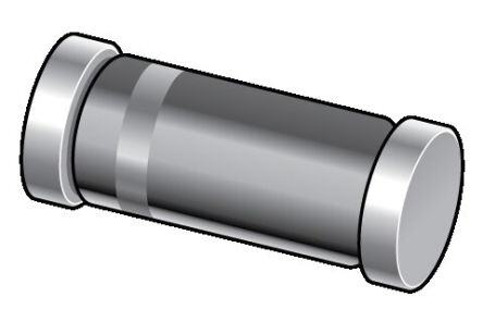
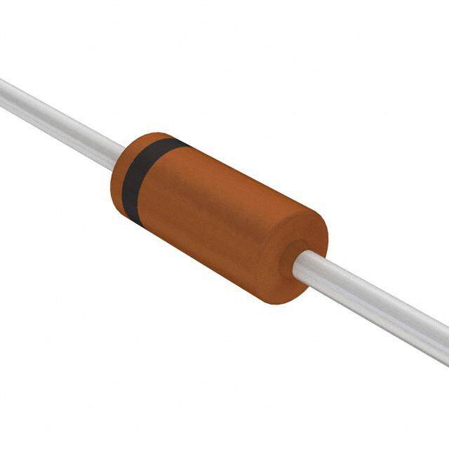
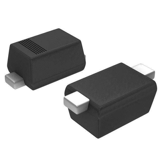
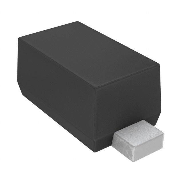
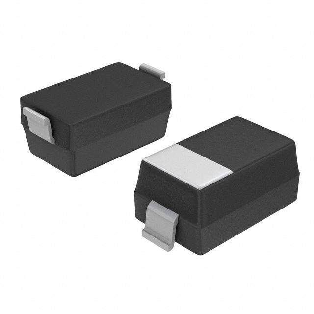
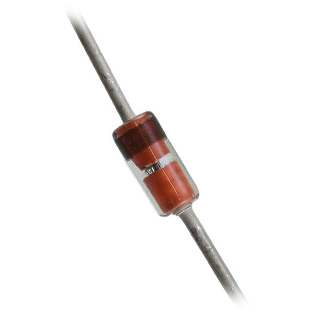
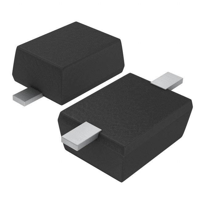
| 产品图片 |
|
| rohs | 符合RoHS无铅 / 符合限制有害物质指令(RoHS)规范要求 |
| 产品系列 | 二极管与整流器,稳压二极管,NXP Semiconductors BZV55-B2V7,115- |
| 数据手册 | |
| 产品型号 | BZV55-B2V7,115 |
| PCN其它 | |
| 不同If时的电压-正向(Vf) | 900mV @ 10mA |
| 不同 Vr时的电流-反向漏电流 | 20µA @ 1V |
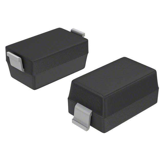
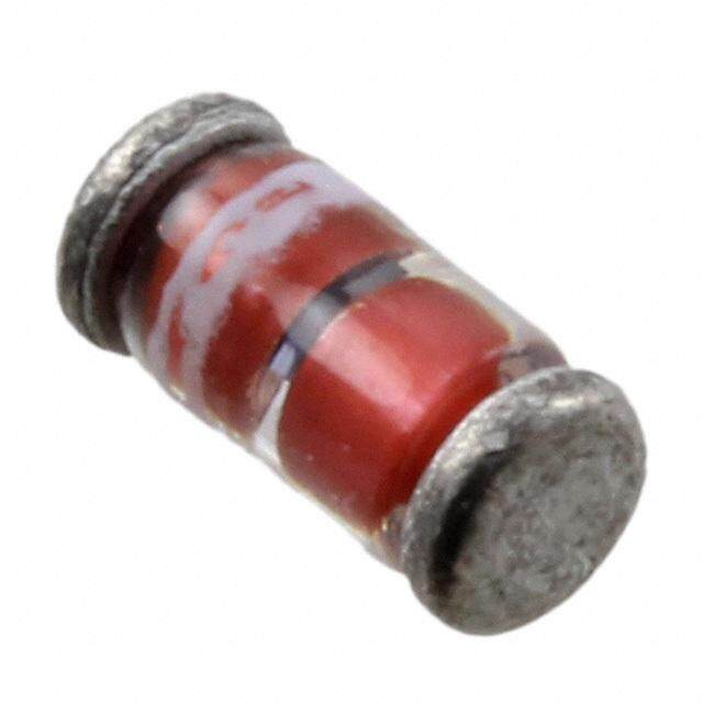
| 产品目录绘图 |
|
| 产品种类 | |
| 供应商器件封装 | LLDS; MiniMelf |
| 其它名称 | 568-6247-6 |
| 功率-最大值 | 500mW |
| 功率耗散 | 500 mW |
| 包装 | Digi-Reel® |
| 商标 | NXP Semiconductors |
| 安装类型 | 表面贴装 |
| 安装风格 | SMD/SMT |
| 容差 | ±2% |
| 封装 | Reel |
| 封装/外壳 | SOD-80C |
| 封装/箱体 | SOD-80 |
| 工作温度 | -65°C ~ 200°C |
| 工厂包装数量 | 2500 |
| 最大反向漏泄电流 | 20 uA |
| 最大工作温度 | + 200 C |
| 最大齐纳阻抗 | 100 Ohms |
| 最小工作温度 | - 65 C |
| 标准包装 | 1 |
| 电压-齐纳(标称值)(Vz) | 2.7V |
| 电压容差 | 2 % |
| 电压温度系数 | - 2 mV/K |
| 配置 | Single |
| 阻抗(最大值)(Zzt) | 100 欧姆 |
| 零件号别名 | BZV55-B2V7 T/R |
| 齐纳电压 | 2.7 V |
| 齐纳电流 | 250 mA |

.jpg)


- 商务部:美国ITC正式对集成电路等产品启动337调查
- 曝三星4nm工艺存在良率问题 高通将骁龙8 Gen1或转产台积电
- 太阳诱电将投资9.5亿元在常州建新厂生产MLCC 预计2023年完工
- 英特尔发布欧洲新工厂建设计划 深化IDM 2.0 战略
- 台积电先进制程称霸业界 有大客户加持明年业绩稳了
- 达到5530亿美元!SIA预计今年全球半导体销售额将创下新高
- 英特尔拟将自动驾驶子公司Mobileye上市 估值或超500亿美元
- 三星加码芯片和SET,合并消费电子和移动部门,撤换高东真等 CEO
- 三星电子宣布重大人事变动 还合并消费电子和移动部门
- 海关总署:前11个月进口集成电路产品价值2.52万亿元 增长14.8%
PDF Datasheet 数据手册内容提取
BZV55 series Voltage regulator diodes Rev. 5 — 26 January 2011 Product data sheet 1. Product profile 1.1 General description Low-power voltage regulator diodes in small hermetically sealed glass SOD80C Surface-Mounted Device (SMD) packages. The diodes are available in the normalized E242%(BZV55-B) and approximately 5%(BZV55-C) tolerance range. Theseriesconsists of 37types with nominal working voltages from 2.4Vto75V. 1.2 Features and benefits Non-repetitive peak reverse power Wide working voltage range: dissipation: 40W nominal2.4Vto75V (E24range) Total power dissipation: 500mW Low differential resistance Two tolerance series: 2%and5% Small hermetically sealed glass SMDpackage 1.3 Applications General regulation functions 1.4 Quick reference data Table 1. Quick reference data Symbol Parameter Conditions Min Typ Max Unit V forward voltage I =10mA - - 0.9 V F F P non-repetitive peak [1] - - 40 W ZSM reversepower dissipation [1] tp=100s; square wave; Tj=25C prior to surge 2. Pinning information Table 2. Pinning Pin Description Simplified outline Graphic symbol 1 cathode [1] 2 anode k a 1 2 006aaa152 [1] The marking band indicates the cathode.
BZV55 series Nexperia Voltage regulator diodes 3. Ordering information Table 3. Ordering information Type number Package Name Description Version BZV55-B2V4 to - hermetically sealed glass surface-mounted SOD80C BZV55-C75[1] package; 2connectors [1] The series consists of 74types with nominal working voltages from 2.4V to75V. 4. Marking Table 4. Marking codes Type number Marking code BZV55-B2V4 to BZV55-C75 marking band 5. Limiting values Table 5. Limiting values In accordance with the Absolute Maximum Rating System (IEC 60134). Symbol Parameter Conditions Min Max Unit I forward current - 250 mA F I non-repetitive peak [1] - see ZSM reversecurrent Table8 and9 P non-repetitive peak [1] - 40 W ZSM reversepower dissipation P total power dissipation T 50C [2] - 400 mW tot amb T 50C [2] - 500 mW tp T storage temperature 65 +200 C stg T junction temperature 65 +200 C j [1] tp=100s; square wave; Tj=25C prior to surge [2] Device mounted on a ceramic substrate of 10100.6mm. 6. Thermal characteristics Table 6. Thermal characteristics Symbol Parameter Conditions Min Typ Max Unit R thermal resistance from in free air [1] - - 380 K/W th(j-a) junction to ambient R thermal resistance from - - 300 K/W th(j-sp) junction to solder point [1] Device mounted on a ceramic substrate of 10100.6mm. BZV55_SER All information provided in this document is subject to legal disclaimers. © Nexperia B.V. 2017. All rights reserved Product data sheet Rev. 5 — 26 January 2011 2 of 13
BZV55 series Nexperia Voltage regulator diodes 103 006aab072 Zth(j-a) δ = 1 (K/W) 0.75 0.50 0.33 102 0.20 0.10 0.05 0.02 10 0.01 ≤ 0.001 1 10−1 1 10 102 103 104 105 tp (ms) Fig 1. Transient thermal impedance from junction to ambient as a function of pulse duration; typicalvalues 7. Characteristics Table 7. Characteristics T =25C unless otherwise specified. j Symbol Parameter Conditions Min Typ Max Unit V forward voltage I =10mA - - 0.9 V F F I reverse current R BZV55-B/C2V4 V =1V - - 50 A R BZV55-B/C2V7 V =1V - - 20 A R BZV55-B/C3V0 V =1V - - 10 A R BZV55-B/C3V3 V =1V - - 5 A R BZV55-B/C3V6 V =1V - - 5 A R BZV55-B/C3V9 V =1V - - 3 A R BZV55-B/C4V3 V =1V - - 3 A R BZV55-B/C4V7 V =2V - - 3 A R BZV55-B/C5V1 V =2V - - 2 A R BZV55-B/C5V6 V =2V - - 1 A R BZV55-B/C6V2 V =4V - - 3 A R BZV55-B/C6V8 V =4V - - 2 A R BZV55-B/C7V5 V =5V - - 1 A R BZV55-B/C8V2 V =5V - - 700 nA R BZV55-B/C9V1 V =6V - - 500 nA R BZV55-B/C10 V =7V - - 200 nA R BZV55-B/C11 V =8V - - 100 nA R BZV55-B/C12 V =8V - - 100 nA R BZV55-B/C13 V =8V - - 100 nA R BZV55-B/C15 to BZV55-B/C75 V =0.7V - - 50 nA R Z(nom) BZV55_SER All information provided in this document is subject to legal disclaimers. © Nexperia B.V. 2017. All rights reserved Product data sheet Rev. 5 — 26 January 2011 3 of 13
BZV55 series Nexperia Voltage regulator diodes Table 8. Characterist ics per type; BZV55-B2V4 to BZV55-C24 T =25C unless otherwise specified. j BZV55- Sel Working Differential resistance Temperature Diode Non-repetitive xxx voltage r () coefficient capacitance peak reverse dif V (V) S (mV/K) C (pF)[1] current Z Z d I (A)[2] I =5mA I =1mA I =5mA I =5mA ZSM Z Z Z Z Min Max Typ Max Typ Max Min Typ Max Max Max 2V4 B 2.35 2.45 275 600 70 100 3.5 1.6 0 450 6.0 C 2.2 2.6 2V7 B 2.65 2.75 300 600 75 100 3.5 2.0 0 450 6.0 C 2.5 2.9 3V0 B 2.94 3.06 325 600 80 95 3.5 2.1 0 450 6.0 C 2.8 3.2 3V3 B 3.23 3.37 350 600 85 95 3.5 2.4 0 450 6.0 C 3.1 3.5 3V6 B 3.53 3.67 375 600 85 90 3.5 2.4 0 450 6.0 C 3.4 3.8 3V9 B 3.82 3.98 400 600 85 90 3.5 2.5 0 450 6.0 C 3.7 4.1 4V3 B 4.21 4.39 410 600 80 90 3.5 2.5 0 450 6.0 C 4.0 4.6 4V7 B 4.61 4.79 425 500 50 80 3.5 1.4 0.2 300 6.0 C 4.4 5.0 5V1 B 5.0 5.2 400 480 40 60 2.7 0.8 1.2 300 6.0 C 4.8 5.4 5V6 B 5.49 5.71 80 400 15 40 2.0 1.2 2.5 300 6.0 C 5.2 6.0 6V2 B 6.08 6.32 40 150 6 10 0.4 2.3 3.7 200 6.0 C 5.8 6.6 6V8 B 6.66 6.94 30 80 6 15 1.2 3.0 4.5 200 6.0 C 6.4 7.2 7V5 B 7.35 7.65 30 80 6 15 2.5 4.0 5.3 150 4.0 C 7.0 7.9 8V2 B 8.04 8.36 40 80 6 15 3.2 4.6 6.2 150 4.0 C 7.7 8.7 9V1 B 8.92 9.28 40 100 6 15 3.8 5.5 7.0 150 3.0 C 8.5 9.6 10 B 9.8 10.2 50 150 8 20 4.5 6.4 8.0 90 3.0 C 9.4 10.6 11 B 10.8 11.2 50 150 10 20 5.4 7.4 9.0 85 2.5 C 10.4 11.6 12 B 11.8 12.2 50 150 10 25 6.0 8.4 10.0 85 2.5 C 11.4 12.7 BZV55_SER All information provided in this document is subject to legal disclaimers. © Nexperia B.V. 2017. All rights reserved Product data sheet Rev. 5 — 26 January 2011 4 of 13
BZV55 series Nexperia Voltage regulator diodes Table 8. Characteristics per type; BZV55-B2V4 to BZV55-C24 …continued T =25C unless otherwise specified. j BZV55- Sel Working Differential resistance Temperature Diode Non-repetitive xxx voltage r () coefficient capacitance peak reverse dif V (V) S (mV/K) C (pF)[1] current Z Z d I (A)[2] I =5mA I =1mA I =5mA I =5mA ZSM Z Z Z Z Min Max Typ Max Typ Max Min Typ Max Max Max 13 B 12.7 13.3 50 170 10 30 7.0 9.4 11.0 80 2.5 C 12.4 14.1 15 B 14.7 15.3 50 200 10 30 9.2 11.4 13.0 75 2.0 C 13.8 15.6 16 B 15.7 16.3 50 200 10 40 10.4 12.4 14.0 75 1.5 C 15.3 17.1 18 B 17.6 18.4 50 225 10 45 12.4 14.4 16.0 70 1.5 C 16.8 19.1 20 B 19.6 20.4 60 225 15 55 12.3 15.6 18.0 60 1.5 C 18.8 21.2 22 B 21.6 22.4 60 250 20 55 14.1 17.6 20.0 60 1.25 C 20.8 23.3 24 B 23.5 24.5 60 250 25 70 15.9 19.6 22.0 55 1.25 C 22.8 25.6 [1] f=1MHz; V =0V R [2] tp=100s; square wave; Tj=25C prior to surge BZV55_SER All information provided in this document is subject to legal disclaimers. © Nexperia B.V. 2017. All rights reserved Product data sheet Rev. 5 — 26 January 2011 5 of 13
BZV55 series Nexperia Voltage regulator diodes Table 9. Characterist ics per type; BZV55-B27 to BZV55-C75 T =25C unless otherwise specified. j BZV55- Sel Working Differential resistance Temperature Diode Non-repetitive xxx voltage r () coefficient capacitance peak reverse dif V (V) S (mV/K) C (pF)[1] current Z Z d I (A)[2] I =2mA I =0.5mA I =2mA I =2mA ZSM Z Z Z Z Min Max Typ Max Typ Max Min Typ Max Max Max 27 B 26.5 27.5 65 300 25 80 18.0 22.7 25.3 50 1.0 C 25.1 28.9 30 B 29.4 30.6 70 300 30 80 20.6 25.7 29.4 50 1.0 C 28.0 32.0 33 B 32.3 33.7 75 325 35 80 23.3 28.7 33.4 45 0.9 C 31.0 35.0 36 B 35.3 36.7 80 350 35 90 26.0 31.8 37.4 45 0.8 C 34.0 38.0 39 B 38.2 39.8 80 350 40 130 28.7 34.8 41.2 45 0.7 C 37.0 41.0 43 B 42.1 43.9 85 375 45 150 31.4 38.8 46.6 40 0.6 C 40.0 46.0 47 B 46.1 47.9 85 375 50 170 35.0 42.9 51.8 40 0.5 C 44.0 50.0 51 B 50.0 52.0 90 400 60 180 38.6 46.9 57.2 40 0.4 C 48.0 54.0 56 B 54.9 57.1 100 425 70 200 42.2 52.0 63.8 40 0.3 C 52.0 60.0 62 B 60.8 63.2 120 450 80 215 58.8 64.4 71.6 35 0.3 C 58.0 66.0 68 B 66.6 69.4 150 475 90 240 65.6 71.7 79.8 35 0.25 C 64.0 72.0 75 B 73.5 76.5 170 500 95 255 73.4 80.2 88.6 35 0.2 C 70.0 79.0 [1] f=1MHz; V =0V R [2] tp=100s; square wave; Tj=25C prior to surge BZV55_SER All information provided in this document is subject to legal disclaimers. © Nexperia B.V. 2017. All rights reserved Product data sheet Rev. 5 — 26 January 2011 6 of 13
BZV55 series Nexperia Voltage regulator diodes 103 mbg801 300 mbg781 PZSM IF (W) (mA) 102 200 (1) 10 100 (2) 1 0 10−1 1 10 0.6 0.8 1 tp (ms) VF (V) (1) Tj=25C (prior to surge) Tj=25C (2) Tj=150C (prior to surge) Fig 2. Non-repetitive peak reverse power dissipation Fig 3. Forward current as a function of forward as a function of pulse duration; maximum voltage; typical values values mbg783 mbg782 0 10 12 SZ SZ 11 (mV/K) 4V3 (mV/K) 10 9V1 −1 5 3V9 8V2 7V5 3V6 6V8 6V2 5V6 5V1 −2 3V3 0 4V7 3V0 2V4 2V7 −3 −5 0 20 40 IZ (mA) 60 0 4 8 12 16IZ (mA)20 BZV55-B/C2V4 to BZV55-B/C4V3 BZV55-B/C4V7 to BZV55-B/C12 Tj=25Cto150C Tj=25Cto150C Fig 4. Temperature coefficient as a function of Fig 5. Temperature coefficient as a function of working current; typical values working current; typical values BZV55_SER All information provided in this document is subject to legal disclaimers. © Nexperia B.V. 2017. All rights reserved Product data sheet Rev. 5 — 26 January 2011 7 of 13
BZV55 series Nexperia Voltage regulator diodes 8. Package outline 1.60 0.3 0.3 1.45 3.7 3.3 Dimensions in mm 06-03-16 Fig 6. Package outline SOD80C 9. Packing information Table 10. Packing methods The indicated -xxx are the last three digits of the 12NC ordering code.[1] Type number Package Description Packing quantity 2500 10000 BZV55-B2V4 to SOD80C 4mm pitch, 8mm tape and reel -115 -135 BZV55-C75 [1] For further information and the availability of packing methods, see Section13. BZV55_SER All information provided in this document is subject to legal disclaimers. © Nexperia B.V. 2017. All rights reserved Product data sheet Rev. 5 — 26 January 2011 8 of 13
BZV55 series Nexperia Voltage regulator diodes 10. Soldering 4.55 4.30 2.30 solder lands solder paste 2.25 1.70 1.60 solder resist occupied area Dimensions in mm 0.90 sod080c (2x) Fig 7. Reflow soldering footprint SOD80C 6.30 4.90 2.70 1.90 solder lands solder resist 2.90 1.70 occupied area tracks Dimensions in mm sod080c Fig 8. Wave soldering footprint SOD80C BZV55_SER All information provided in this document is subject to legal disclaimers. © Nexperia B.V. 2017. All rights reserved Product data sheet Rev. 5 — 26 January 2011 9 of 13
BZV55 series Nexperia Voltage regulator diodes 11. Revision history Table 11. Revision history Document ID Release date Data sheet status Change notice Supersedes BZV55_SERv.5 20110126 Product data sheet - BZV55_SERv.4 Modifications: • Section 4 “Marking”: updated • Table 6 “Thermal characteristics”: changed R for R th(j-t) th(j-sp) • Figure6: superseded by minimized outline drawing • Section 12 “Legal information”: updated BZV55_SERv.4 20070719 Product data sheet CPCN200508022F BZV55v.3 BZV55v.3 20020228 Product specification - BZV55v.2 BZV55v.2 19990521 Product specification - BZV55v.1 BZV55v.1 19960426 Product specification - - BZV55_SER All information provided in this document is subject to legal disclaimers. © Nexperia B.V. 2017. All rights reserved Product data sheet Rev. 5 — 26 January 2011 10 of 13
BZV55 series Nexperia Voltage regulator diodes 12. Legal information 12.1 Data sheet status Document status[1][2] Product status[3] Definition Objective [short] data sheet Development This document contains data from the objective specification for product development. Preliminary [short] data sheet Qualification This document contains data from the preliminary specification. Product [short] data sheet Production This document contains the product specification. [1] Please consult the most recently issued document before initiating or completing a design. [2] The term ‘short data sheet’ is explained in section “Definitions”. [3] The product status of device(s) described in this document may have changed since this document was published and may differ in case of multiple devices. The latest product status information is available on the Internet at URLhttp://www.nexperia.com. 12.2 Definitions malfunction of a Nexperia product can reasonably be expected to result in personal injury, death or severe property or environmental damage. Nexperia accepts no liability for inclusion and/or use of Draft — The document is a draft version only. The content is still under Nexperia products in such equipment or applications and internal review and subject to formal approval, which may result in therefore such inclusion and/or use is at the customer’s own risk. modifications or additions. Nexperia does not give any representations or warranties as to the accuracy or completeness of Applications — Applications that are described herein for any of these information included herein and shall have no liability for the consequences of products are for illustrative purposes only. Nexperia makes no use of such information. representation or warranty that such applications will be suitable for the specified use without further testing or modification. Short data sheet — A short data sheet is an extract from a full data sheet with the same product type number(s) and title. A short data sheet is intended Customers are responsible for the design and operation of their applications for quick reference only and should not be relied upon to contain detailed and and products using Nexperia products, and Nexperia full information. For detailed and full information see the relevant full data accepts no liability for any assistance with applications or customer product sheet, which is available on request via the local Nexperia sales design. It is customer’s sole responsibility to determine whether the Nexperia office. In case of any inconsistency or conflict with the short data sheet, the product is suitable and fit for the customer’s applications and full data sheet shall prevail. products planned, as well as for the planned application and use of customer’s third party customer(s). Customers should provide appropriate Product specification — The information and data provided in a Product design and operating safeguards to minimize the risks associated with their data sheet shall define the specification of the product as agreed between applications and products. Nexperia and its customer, unless Nexperia and Nexperia does not accept any liability related to any default, customer have explicitly agreed otherwise in writing. In no event however, damage, costs or problem which is based on any weakness or default in the shall an agreement be valid in which the Nexperia product is customer’s applications or products, or the application or use by customer’s deemed to offer functions and qualities beyond those described in the third party customer(s). Customer is responsible for doing all necessary Product data sheet. testing for the customer’s applications and products using Nexperia products in order to avoid a default of the applications and 12.3 Disclaimers the products or of the application or use by customer’s third party customer(s). Nexperia does not accept any liability in this respect. Limited warranty and liability — Information in this document is believed to Limiting values — Stress above one or more limiting values (as defined in be accurate and reliable. However, Nexperia does not give any the Absolute Maximum Ratings System of IEC60134) will cause permanent representations or warranties, expressed or implied, as to the accuracy or damage to the device. Limiting values are stress ratings only and (proper) completeness of such information and shall have no liability for the operation of the device at these or any other conditions above those given in consequences of use of such information. the Recommended operating conditions section (if present) or the Characteristics sections of this document is not warranted. Constant or In no event shall Nexperia be liable for any indirect, incidental, repeated exposure to limiting values will permanently and irreversibly affect punitive, special or consequential damages (including - without limitation - lost the quality and reliability of the device. profits, lost savings, business interruption, costs related to the removal or replacement of any products or rework charges) whether or not such Terms and conditions of commercial sale — Nexperia damages are based on tort (including negligence), warranty, breach of products are sold subject to the general terms and conditions of commercial contract or any other legal theory. sale, as published at http://www.nexperia.com/profile/terms, unless otherwise Notwithstanding any damages that customer might incur for any reason agreed in a valid written individual agreement. In case an individual whatsoever, Nexperia’s aggregate and cumulative liability towards agreement is concluded only the terms and conditions of the respective customer for the products described herein shall be limited in accordance agreement shall apply. Nexperia hereby expressly objects to with the Terms and conditions of commercial sale of Nexperia. applying the customer’s general terms and conditions with regard to the purchase of Nexperia products by customer. Right to make changes — Nexperia reserves the right to make changes to information published in this document, including without No offer to sell or license — Nothing in this document may be interpreted or limitation specifications and product descriptions, at any time and without construed as an offer to sell products that is open for acceptance or the grant, notice. This document supersedes and replaces all information supplied prior conveyance or implication of any license under any copyrights, patents or to the publication hereof. other industrial or intellectual property rights. Suitability for use — Nexperia products are not designed, Export control — This document as well as the item(s) described herein authorized or warranted to be suitable for use in life support, life-critical or may be subject to export control regulations. Export might require a prior safety-critical systems or equipment, nor in applications where failure or authorization from national authorities. BZV55_SER All information provided in this document is subject to legal disclaimers. © Nexperia B.V. 2017. All rights reserved Product data sheet Rev. 5 — 26 January 2011 11 of 13
BZV55 series Nexperia Voltage regulator diodes Quick reference data — The Quick reference data is an extract of the product for such automotive applications, use and specifications, and (b) product data given in the Limiting values and Characteristics sections of this whenever customer uses the product for automotive applications beyond document, and as such is not complete, exhaustive or legally binding. Nexperia’s specifications such use shall be solely at customer’s own risk, and (c) customer fully indemnifies Nexperia for any Non-automotive qualified products — Unless this data sheet expressly liability, damages or failed product claims resulting from customer design and states that this specific Nexperia product is automotive qualified, use of the product for automotive applications beyond Nexperia’s the product is not suitable for automotive use. It is neither qualified nor tested standard warranty and Nexperia’s product specifications. in accordance with automotive testing or application requirements. Nexperia accepts no liability for inclusion and/or use of non-automotive qualified products in automotive equipment or applications. 12.4 Trademarks In the event that customer uses the product for design-in and use in automotive applications to automotive specifications and standards, customer Notice: All referenced brands, product names, service names and trademarks (a) shall use the product without Nexperia’s warranty of the are the property of their respective owners. 13. Contact information For more information, please visit: http://www.nexperia.com For sales office addresses, please send an email to: salesaddresses@nexperia.com BZV55_SER All information provided in this document is subject to legal disclaimers. © Nexperia B.V. 2017. All rights reserved Product data sheet Rev. 5 — 26 January 2011 12 of 13
BZV55 series Nexperia Voltage regulator diodes 14. Contents 1 Product profile. . . . . . . . . . . . . . . . . . . . . . . . . . 1 1.1 General description . . . . . . . . . . . . . . . . . . . . . 1 1.2 Features and benefits. . . . . . . . . . . . . . . . . . . . 1 1.3 Applications . . . . . . . . . . . . . . . . . . . . . . . . . . . 1 1.4 Quick reference data . . . . . . . . . . . . . . . . . . . . 1 2 Pinning information. . . . . . . . . . . . . . . . . . . . . . 1 3 Ordering information. . . . . . . . . . . . . . . . . . . . . 2 4 Marking. . . . . . . . . . . . . . . . . . . . . . . . . . . . . . . . 2 5 Limiting values. . . . . . . . . . . . . . . . . . . . . . . . . . 2 6 Thermal characteristics . . . . . . . . . . . . . . . . . . 2 7 Characteristics. . . . . . . . . . . . . . . . . . . . . . . . . . 3 8 Package outline. . . . . . . . . . . . . . . . . . . . . . . . . 8 9 Packing information . . . . . . . . . . . . . . . . . . . . . 8 10 Soldering . . . . . . . . . . . . . . . . . . . . . . . . . . . . . . 9 11 Revision history. . . . . . . . . . . . . . . . . . . . . . . . 10 12 Legal information. . . . . . . . . . . . . . . . . . . . . . . 11 12.1 Data sheet status . . . . . . . . . . . . . . . . . . . . . . 11 12.2 Definitions. . . . . . . . . . . . . . . . . . . . . . . . . . . . 11 12.3 Disclaimers. . . . . . . . . . . . . . . . . . . . . . . . . . . 11 12.4 Trademarks. . . . . . . . . . . . . . . . . . . . . . . . . . . 12 13 Contact information. . . . . . . . . . . . . . . . . . . . . 12 14 Contents. . . . . . . . . . . . . . . . . . . . . . . . . . . . . . 13 © Nexperia B.V. 2017. All rights reserved For more information, please visit: http://www.nexperia.com For sales office addresses, please send an email to: salesaddresses@nexperia.com Date of release: 26 January 2011