ICGOO在线商城 > 集成电路(IC) > PMIC - 稳压器 - 线性 > BU10TD3WG-TR
 Datasheet下载
- 型号: BU10TD3WG-TR
- 制造商: ROHM Semiconductor
- 库位|库存: xxxx|xxxx
- 要求:
| 数量阶梯 | 香港交货 | 国内含税 |
| +xxxx | $xxxx | ¥xxxx |
查看当月历史价格
查看今年历史价格
BU10TD3WG-TR产品简介:
ICGOO电子元器件商城为您提供BU10TD3WG-TR由ROHM Semiconductor设计生产,在icgoo商城现货销售,并且可以通过原厂、代理商等渠道进行代购。 BU10TD3WG-TR价格参考¥1.00-¥1.00。ROHM SemiconductorBU10TD3WG-TR封装/规格:PMIC - 稳压器 - 线性, Linear Voltage Regulator IC Positive Fixed 1 Output 1V 200mA 5-SSOP。您可以下载BU10TD3WG-TR参考资料、Datasheet数据手册功能说明书,资料中有BU10TD3WG-TR 详细功能的应用电路图电压和使用方法及教程。
BU10TD3WG-TR 是由罗姆半导体(Rohm Semiconductor)生产的一款线性稳压器,属于电源管理集成电路(PMIC)的一部分。该器件主要用于提供稳定的输出电压,适用于对电源噪声敏感、要求高稳定性的电子设备中。

该型号稳压器的典型应用场景包括:

1. 便携式电子产品:如智能手机、平板电脑和可穿戴设备,用于为内部处理器、传感器等模块提供稳定电源。
2. 音频设备:由于线性稳压器具有较低的输出噪声,适合用于高保真音频放大器或录音设备中,以提升音质表现。
3. 工业控制系统:用于为工业传感器、测量仪器和控制模块供电,确保在复杂电磁环境中保持稳定运行。
4. 汽车电子系统:可用于车载信息娱乐系统、仪表盘控制模块等场景,满足车载环境对可靠性和稳定性的要求。
5. 通信设备:如无线基站、路由器和光模块等,为敏感的射频和模拟电路提供干净的电源。

BU10TD3WG-TR 采用小型封装,具备良好的热稳定性和负载调节能力,适合空间受限但对性能有较高要求的设计。
| 参数 | 数值 |
| 产品目录 | 集成电路 (IC)半导体 |
| 描述 | IC REG LDO 1V 0.2A 5SSOP低压差稳压器 Standard CMOS LDO Vreg; 1.0V |
| 产品分类 | |
| 品牌 | Rohm Semiconductor |
| 产品手册 | |
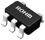
| 产品图片 |
|
| rohs | 符合RoHS无铅 / 符合限制有害物质指令(RoHS)规范要求 |
| 产品系列 | 电源管理 IC,低压差稳压器,ROHM Semiconductor BU10TD3WG-TR- |
| 数据手册 | |
| 产品型号 | BU10TD3WG-TR |
| 产品种类 | 低压差稳压器 |
| 供应商器件封装 | 5-SSOP |
| 其它名称 | BU10TD3WG-TR-ND |
| 包装 | 带卷 (TR) |
| 商标 | ROHM Semiconductor |
| 回动电压—最大值 | 540 mV |
| 安装类型 | 表面贴装 |
| 安装风格 | SMD/SMT |
| 封装 | Reel |
| 封装/外壳 | 6-TFSOP(0.063",1.60mm 宽),5 引线 |
| 封装/箱体 | SSOP-5 |
| 工作温度 | -40°C ~ 85°C |
| 工厂包装数量 | 3000 |
| 最大功率耗散 | 540 mW |
| 最大工作温度 | + 85 C |
| 最大输入电压 | 6.5 V |
| 最小工作温度 | - 40 C |
| 标准包装 | 3,000 |
| 特色产品 | http://www.digikey.com/product-highlights/cn/zh/rohm-cmos-ldo-regulators/2469 |
| 电压-跌落(典型值) | 0.8V @ 200mA |
| 电压-输入 | 1.7 V ~ 5.5 V |
| 电压-输出 | 1V |
| 电流-输出 | 200mA |
| 电流-限制(最小值) | 220mA |
| 稳压器拓扑 | 正,固定式 |
| 稳压器数 | 1 |
| 负载调节 | 10 mV |
| 输出电压 | 1 V |
| 输出电流 | 200 mA |


- 商务部:美国ITC正式对集成电路等产品启动337调查
- 曝三星4nm工艺存在良率问题 高通将骁龙8 Gen1或转产台积电
- 太阳诱电将投资9.5亿元在常州建新厂生产MLCC 预计2023年完工
- 英特尔发布欧洲新工厂建设计划 深化IDM 2.0 战略
- 台积电先进制程称霸业界 有大客户加持明年业绩稳了
- 达到5530亿美元!SIA预计今年全球半导体销售额将创下新高
- 英特尔拟将自动驾驶子公司Mobileye上市 估值或超500亿美元
- 三星加码芯片和SET,合并消费电子和移动部门,撤换高东真等 CEO
- 三星电子宣布重大人事变动 还合并消费电子和移动部门
- 海关总署:前11个月进口集成电路产品价值2.52万亿元 增长14.8%


PDF Datasheet 数据手册内容提取
Datasheet CMOS LDO Regulator Series for Portable Equipments Versatile Package FULL CMOS LDO Regulator BUxxTD2WNVX series ●General Description ●Key Specifications BUxxTD2WNVX series is high-performance FULL CMOS (cid:132) Output voltage: 1.0V to 3.4V regulator with 200-mA output, which is mounted on (cid:132) Accuracy output voltage: ±1.0% (±25mV) versatile package SSON004X1010 (1.00mm × 1.00 mm (cid:132) Low current consumption: 35μA × 0.60mm). It has excellent noise characteristics and (cid:132) Operating temperature range: -40°C to +85°C load responsiveness characteristics despite its low circuit current consumption of 35μA. It is most appropriate for ●Applications various applications such as power supplies for logic IC, Battery-powered portable equipment, etc. RF, and camera modules.ROHM’s. ●Package SSON004X1010 : 1.00mm x 1.00mm x 0.60mm ●Features (cid:132) High accuracy detection (cid:132) low current consumption (cid:132) Compatible with small ceramic capacitor(Cin=Co=0.47uF) (cid:132) With built-in output discharge circuit (cid:132) High ripple rejection (cid:132) ON/OFF control of output voltage (cid:132) With built-in over current protection circuit and thermal shutdown circuit (cid:132) Low dropout voltage ●Typical Application Circuit STBY STBY VOUT VOUT VIN VIN GND GND GND Fig.1 Application Circuit ○Product structure:Silicon monolithic integrated circuit ○This product is not designed protection against radioactive rays. www.rohm.com © 2013 ROHM Co., Ltd. All rights reserved. TSZ02201-0RBR0A300050-1-2 TSZ22111・14・001 1/40 14.Jan.2013.Rev.008
BUxxTD2WNVX series Datasheet ●Connection Diagram SSON004X1010 (TOP VIEW) BOTTOM VIEW 4 VIN 3 STBY 1 VOUT 2 GND LOT Number reverse FIN 1 2 Part Number Marking 1 VOUT 2 GND 4 VIN 3 STBY 1PIN MARK ●Pin Descriptions SSON004X1010 PIN No. Symbol Function 1 VOUT Output Voltage 2 GND Grouding ON/OFF control of output voltage 3 STBY (High: ON, Low: OFF) 4 VIN Power Supply Voltage reverse FIN Substrate (Connect to GND) ●Ordering Information B U x x T D 2 W N V X - T L Part Output Voltage Low Dropout Voltage with Package Packageing and forming specification Number 10 : 1.0V Maximum Output Current output discharge NVX : SSON004X1010 Embossed tape and reel 200mA TL : The pin number 1 is the lower left 34 : 3.4V SSON004X1010 1.0±0.1 <Tape and Reel information> 1PIN MARK Tape Embossed carrier tape ±1.00.1 Quantity 5000pcs X TL ±0.320.1 00..40.6MA08±5405.0º510.65±0.025 +0.03R3−-0.0200.02C.005.(0.12)18 S Dofi rfeecetdion (Treheel odnir ethcteio lne fits h tahned 1 apnind oyfo pur opduull cot uist tahte t htaep leo woenr t hleeft lewfht ehna nydou hold ) 0.480±0..20554±0.05 3 ±0.070.1±0.250.1 (Unit : mm) Reel ∗ O1rpdienr quantity needs to be muDltiiprelec otifo tnh eo mf fineiemdum quantity. www.rohm.com © 2013 ROHM Co., Ltd. All rights reserved. TSZ02201-0RBR0A300050-1-2 TSZ22111・15・001 2/40 14.Jan.2013.Rev.008
BUxxTD2WNVX series Datasheet ●Lineup Marking A 6 5 2 B 3 5i C D Output Voltage 1.0V 1.05V 1.1V 1.15V 1.2V 1.25V 1.3V 1.5V 1.8V Part Number BU10 BU1A BU11 BU1B BU12 BU1C BU13 BU15 BU18 E F G r 0 1 H J K 1.85V 1.9V 2.0V 2.05V 2.1V 2.3V 2.5V 2.6V 2.7V BU1J BU19 BU20 BU2A BU21 BU23 BU25 BU26 BU27 a L M N P Q R U Y 2.75V 2.8V 2.85V 2.9V 3.0V 3.1V 3.2V 3.3V 3.4V BU2H BU28 BU2J BU29 BU30 BU31 BU32 BU33 BU34 ●Absolute Maximum Ratings (Ta=25°C) PARAMETER Symbol Limit Unit Power Supply Voltage VMAX -0.3 ~ +6.5 V Power Dissipation Pd 560(*1) mW Maximum junction temperature TjMAX +125 ℃ Operating Temperature Range Topr -40 ~ +85 ℃ Storage Temperature Range Tstg -55 ~ +125 ℃ (*1)Pd deleted at 5.6mW/℃ at temperatures above Ta=25℃, mounted on 70×70×1.6 mm glass-epoxy PCB. ● RECOMMENDED OPERATING RANGE (not to exceed Pd) PARAMETER Symbol Limit Unit Power Supply Voltage VIN 1.7~6.0 V Maximum Output Current IMAX 200 mA ●OPERATING CONDITIONS PARAMETER Symbol MIN. TYP. MAX. Unit CONDITION Input Capacitor Cin 0.22(*2) 0.47 - μF Ceramic capacitor recommended Output Capacitor Co 0.22(*2) 0.47 - μF (*2)Make sure that the output capacitor value is not kept lower than this specified level across a variety of temperature, DC bias, changing as time progresses characteristic. www.rohm.com © 2013 ROHM Co., Ltd. All rights reserved. TSZ02201-0RBR0A300050-1-2 TSZ22111・15・001 3/40 14.Jan.2013.Rev.008
BUxxTD2WNVX series Datasheet ●Electrical Characteristics (Ta=25℃, VIN=VOUT+1.0V (*3), STBY=VIN, Cin=0.47μF, Co=0.47μF, unless otherwise noted.) Limit PARAMETER Symbol Unit Conditions MIN. TYP. MAX. Overall Device VOUT×0.99 VOUT×1.01 IOUT=10μA, VOUT≧2.5V Output Voltage VOUT VOUT V VOUT-25mV VOUT+25mV IOUT=10μA, VOUT<2.5V Operating Current IIN - 35 60 μA IOUT=0mA Operating Current (STBY) ISTBY - - 1.0 μA STBY=0V Ripple Rejection Ratio RR 45 70 - dB VRR=-20dBv, fRR=1kHz, IOUT=10mA - 800 1100 mV 1.0V≦VOUT<1.2V(IOUT=200mA) - 600 900 mV 1.2V≦VOUT<1.5V(IOUT=200mA) - 440 700 mV 1.5V≦VOUT<1.8V(IOUT=200mA) - 380 600 mV 1.8V≦VOUT<2.5V(IOUT=200mA) Dropout Voltage VSAT - 280 540 mV 2.5V≦VOUT≦2.6V(IOUT=200mA) - 260 500 mV 2.7V≦VOUT≦2.85V(IOUT=200mA) - 240 460 mV 2.9V≦VOUT≦3.1V(IOUT=200mA) - 220 420 mV 3.2V≦VOUT≦3.4V(IOUT=200mA) Line Regulation VDL - 2 20 mV VIN=VOUT+1.0V to 5.5V (*4), IOUT=10μA Load Regulation VDLO - 10 80 mV IOUT=0.01mA to 100mA Over Current Protection (OCP) Limit Current ILMAX 220 400 700 mA Vo=VOUT*0.95 Short Current ISHORT 20 70 150 mA Vo=0V Standby Block Discharge Resistor RDSC 20 50 80 Ω VIN=4.0V, STBY=0V, VOUT=4.0V STBY Pin Pull-down Current ISTB 0.1 0.6 2.0 μA STBY=1.5V ON VSTBH 1.2 - 6.0 V STBY Control Voltage OFF VSTBL -0.3 - 0.3 V This product is not designed for protection against radioactive rays. (*3) VIN=2.5V for VOUT≦1.5V (*4) VIN=2.5V to 3.6V for VOUT≦1.5V ●Block Diagrams VIN VIN 4 VREF Cin VOUT VOUT 1 GND 2 OCP Co TSD STBY STBY STBY Discharge Cin・・・0.47μF (Ceramic) 3 Co ・・・0.47μF (Ceramic) Fig. 2 Block Diagrams www.rohm.com © 2013 ROHM Co., Ltd. All rights reserved. TSZ02201-0RBR0A300050-1-2 TSZ22111・15・001 4/40 14.Jan.2013.Rev.008
BUxxTD2WNVX series Datasheet BU12TD2WNVX ●Reference data (Ta=25ºC unless otherwise specified.) 1.4 1.25 100 1.2 Temp=25°C 1.24 Temp=25°C VIN=STBY Io=0uA Output Voltage (V) 0001....4680 IIIIoooo====0152u000A0m0umAAA Output Voltage (V) 1111111.......11122227890123 IIIooo===015u00A0muAA Gnd Current (uA) 24680000 TTeTememmpp=p=-=248505°°°CC 0.2 VIN=STBY 1.16 Io=200mA VIN=STBY 0.0 1.15 0 0 0.5 1 1.5 2 2.5 3 3.5 4 4.5 5 5.5 1.1 1.2 1.3 1.4 1.5 1.6 1.7 1.8 1.9 2 0 0.5 1 1.5 2 2.5 3 3.5 4 4.5 5 5.5 Input Voltage (V) Input Voltage (V) Input Voltage (V) Fig 3. Output Voltage Fig 4. Line Regulation Fig 5. Circuit Current IGND 1.25 1.6 100 VIN=2.5V 1.24 VIN=2.5V STBY Pin Current (uA) 000111......468024 Temp=25°TCemp=85°C Temp=-40°C Gnd Current (uA) 24680000 STBY=1.T5Vemp=25T°eCmp=8T5°eCmp=-40°C Output Voltage (V) 1111111.......11122227890123 TemSp=T-B4Y0=°C1.5V Temp=25°C Temp=85°C 0.2 1.16 0.0 0 1.15 0 0.5 1 1.5 2 2.5 3 3.5 4 4.5 5 5.5 0 0.05 0.1 0.15 0.2 0 0.05 0.1 0.15 0.2 Input Voltage (V) Output Current (A) Output Current (A) Fig 6. VSTBY - ISTBY Fig 7. IOUT - IGND Fig 8. Load Regulation 1.4 1.25 Temp=25°C 1.5 1.2 VIN=2.5V 1.24 SVTIBNY==21.5.5VV Output Voltage (V) 0001....4680 VIN=1.7V VIN=5.5VVIN=2.5V Output Voltage (V) 01..50 Io=0TTmeeAmmpp==2855°°CC Temp=-40°C Output Voltage (V) 111111......112222890123 Io=0.1mA 1.17 0.2 STBY=1.5V 1.16 0.0 0.0 1.15 0 0.1 0.2 0.3 0.4 0.5 0.6 0 0.5 1 1.5 -40 -15 10 35 60 85 Output Current (A) STBY Voltage (V) Temp (°C) Fig 9. OCP Threshold Fig 10. STBY Threshold Fig 11. VOUT - Temp 60 VIN=2.5V 1.0 50 STBY=1.5V 0.9 VIN=2.5V uA) 40 Io=0mA uA) 00..78 STBY=0V Gnd Current ( 2300 Gnd Current ( 0000....3456 0.2 10 0.1 0 0.0 -40 -15 10 35 60 85 -40 -15 10 35 60 85 Temp (°C) Temp (°C) Fig 12. IGND vs Temp Fig 13. IGND - Temp (STBY) www.rohm.com © 2013 ROHM Co., Ltd. All rights reserved. TSZ02201-0RBR0A300050-1-2 TSZ22111・15・001 5/40 14.Jan.2013.Rev.008
BUxxTD2WNVX series Datasheet BU12TD2WNVX ●Reference data (Ta=25ºC unless otherwise specified.) IOUT=0mA→50mA 15000 0 Output Current (mA) IOUT=50mA→0mA 15000 0 Output Current (mA) Output Voltage (V) 1111....11225005 Output Voltage (V) 1111....21230550 Fig 14. Load Response Fig 15. Load Response IOUT=0mA→100mA 15000 0 Output Current (m IOUT=100mA→0mA 15000 0 Output Current (m A) A) Output Voltage (V) 1111....11225005 Output Voltage (V) 1111....21230550 Fig 16. Load Response Fig 17. Load Response IOUT=0mA→200mA 12000 00 Output Current (m IOUT=200mA→0mA 12000 00 Output Current (m A) A) Output Voltage (V) 1111....10230000 Output Voltage (V) 1111....21340000 Fig 18. Load Response Fig 19. Load Response O O IOUT=50mA→100mA 100 utput C IOUT=100mA→50mA 100 utput C 500 urrent (m 500 urrent (m A A ) ) Output Voltage (V) 1111....11225005 Output Voltage (V) 1111....11225005 Fig 20. Load Response Fig 21. Load Response www.rohm.com © 2013 ROHM Co., Ltd. All rights reserved. TSZ02201-0RBR0A300050-1-2 TSZ22111・15・001 6/40 14.Jan.2013.Rev.008
BUxxTD2WNVX series Datasheet BU12TD2WNVX ●Reference data (Ta=25ºC unless otherwise specified.) 2.0 STB 2.0 STB STBY=0→1.5V 01..00 Y Voltage (V) STBY=0→1.5V 01..00 Y Voltage (V) Output Voltage (V) 012...000 Output Voltage (V) 012...000 Fig 22. Start Up Time Fig 23. Start Up Time Iout=0mA Iout=200mA 4.0 STB 4.0 STB VIN=STBY=0→2.5V 02..00 Y Voltage (V) VIN=STBY=0→2.5V 02..00 Y Voltage (V) Voltage (V) 12..00 Voltage (V) 12..00 Output 0.0 Output 0.0 Fig 24. Start Up Time Fig 25. Start Up Time (VIN=STBY) Iout=0mA (VIN=STBY) Iout=200mA Iout=0mA STBY=1.5→0V 201...000 STBY Voltage (V) VIN=2.5V→3.5V→2.5V 423...555 Input Voltage (V) Output Voltage (V) 012...000 put Voltage (V) 111...122901 ut O1.18 Fig 26. Discharge Time Fig 27. VIN Response www.rohm.com © 2013 ROHM Co., Ltd. All rights reserved. TSZ02201-0RBR0A300050-1-2 TSZ22111・15・001 7/40 14.Jan.2013.Rev.008
BUxxTD2WNVX series Datasheet BU15TD2WNVX ●Reference data (Ta=25ºC unless otherwise specified.) 2.0 1.55 100 1.8 Temp=25°C 1.54 Temp=25°C VIN=STBY IO=0uA VIN=STBY Voltage (V) 1111....0246 Voltage (V) 1111....55550123 urrent (uA) 6800 TTeemmpp==8255°°CC Output 000...468 IIIIoooo====0521u000Am00muAAA Output 111...444789 IIIooo===1050u00AmuAA Gnd C 2400 0.2 1.46 Io=200mA Temp=-40°C 0.0 1.45 0 0 0.5 1 1.5 2 2.5 3 3.5 4 4.5 5 5.5 1.4 1.5 1.6 1.7 1.8 1.9 2 2.1 0 0.5 1 1.5 2 2.5 3 3.5 4 4.5 5 5.5 Input Voltage (V) Input Voltage (V) Input Voltage (V) Fig 28. Output Voltage Fig 29. Line Regulation Fig 30. Circuit Current IGND 1.6 100 1.55 STBY Pin Current (uA) 0000111.......2468024 Temp=25°TCemp=85°C Temp=-40°C Gnd Current (uA) 24680000 SVTIBNY==21.5.T5VVemp=2T5°eCmp=8T5°eCmp=-40°C Output Voltage (V) 111111111.........444455555678901234 STVTeImBNYp===2-1.45.50VV°CTemp=25°C Temp=85°C 0.0 0 1.45 0 0.5 1 1.5 2 2.5 3 3.5 4 4.5 5 5.5 0 0.05 0.1 0.15 0.2 0 0.05 0.1 0.15 0.2 Input Voltage (V) Output Current (A) Output Current (A) Fig 31. VSTBY - ISTBY Fig 32. IOUT - IGND Fig 33. Load Regulation 1.55 2.0 2.0 VIN=2.5V 1.8 Temp=25°C VIN=3.8V 1.54 STBY=1.5V Output Voltage (V) 0001111.......4680246 VIN=2.0V VIN=V5IN.5=V2.5V Output Voltage (V) 011...505 Io=0TTmeeAmmpp==2855°°CC Temp=-40°C Output Voltage (V) 1111111.......44455557890123 Io=0.1mA 0.2 STBY=1.5V 1.46 0.0 0.0 1.45 0 0.1 0.2 0.3 0.4 0.5 0.6 0 0.5 1 1.5 -40 -15 10 35 60 85 Output Current (A) STBY Voltage (V) Temp (°C) Fig 34. OCP Threshold Fig 35. STBY Threshold Fig 36. VOUT - Temp 60 1.0 VIN=2.5V 0.9 VIN=2.5V 50 STBY=1.5V 0.8 STBY=0V A) Io=0mA A) ent (u 40 ent (u 00..67 Gnd Curr 2300 Gnd Curr 000...345 0.2 10 0.1 0 0.0 -40 -15 10 35 60 85 -40 -15 10 35 60 85 Temp (°C) Temp (°C) Fig 37. IGND vs Temp Fig 38. IGND vs Temp (STBY) www.rohm.com © 2013 ROHM Co., Ltd. All rights reserved. TSZ02201-0RBR0A300050-1-2 TSZ22111・15・001 8/40 14.Jan.2013.Rev.008
BUxxTD2WNVX series Datasheet BU15TD2WNVX ●Reference data (Ta=25ºC unless otherwise specified.) 100 Output C 110000 Output COutput C IOUT=0mA→50mA 500 urrent (m IOUT=50mA→0mA 550000 urrent (murrent (m A AA Output Voltage (V) 1111....44555005 ) Output Voltage (V) Output Voltage (V) 11111111........5421562305055050 ) ) Fig 39. Load Response Fig 40. Load Response IOUT=0mA→100mA 15000 0 Output Current (m IOUT=100mA→0mA 1155000000 00 Output Current (mOutput Current (m Output Voltage (V) 1111....44555005 A) Output Voltage (V) Output Voltage (V) 11111111........5421562305055050 A) A) Fig 41. Load Response Fig 42. Load Response IOUT=0mA→200mA 21000 00 Output Current (m IOUT=200mA→0mA 2121000000 0000 Output Current (mOutput Current (m Output Voltage (V) 1111....43560000 A) Output Voltage (V) Output Voltage (V) 11111111......54..67213400000000 A) A) Fig 43. Load Response Fig 44. Load Response IOUT=50mA→100mA 15000 0 Output Current (m IOUT=100mA→50mA 15000 0 Output Current (m A A Output Voltage (V) 1111....44555005 ) Output Voltage (V) 1111....54560550 ) Fig 45. Load Response Fig 46. Load Response www.rohm.com © 2013 ROHM Co., Ltd. All rights reserved. TSZ02201-0RBR0A300050-1-2 TSZ22111・15・001 9/40 14.Jan.2013.Rev.008
BUxxTD2WNVX series Datasheet BU15TD2WNVX ●Reference data (Ta=25ºC unless otherwise specified.) 2.0 STB 2.0 STB Output Voltage (V) 012...000 STBY=0→1.5V 10..00 Y Voltage (V) Output Voltage (V) 012...000 STBY=0→1.5V 10..00 Y Voltage (V) Fig 47. Start Up Time Fig 48. Start Up Time Iout=0mA Iout=200mA Output Voltage (V) 012...000 VIN=STBY=0→2.5V 240...000 STBY Voltage (V) Output Voltage (V) 012...000 VIN=STBY=0→2.5V 240...000 STBY Voltage (V) Fig 49. Start Up Time Fig 50. Start Up Time (VIN=STBY) Iout=0mA (VIN=STBY) Iout=200mA Iout=0mA STBY=1.5→0V 120...000 STBY Voltage (V) VIN=2.5V→3.5V→2.5V 342...555 Input Voltage (V) Output Voltage (V) 012...000 utput Voltage (V) 111...455901 O1.48 Fig 51. Discharge Time Fig 52. VIN Response www.rohm.com © 2013 ROHM Co., Ltd. All rights reserved. TSZ02201-0RBR0A300050-1-2 TSZ22111・15・001 10/40 14.Jan.2013.Rev.008
BUxxTD2WNVX series Datasheet BU18TD2WNVX ●Reference data (Ta=25ºC unless otherwise specified.) 2.0 1.85 100 1.8 Temp=25°C 1.84 Temp=25°C VIN=STBY Io=0uA VIN=STBY Output Voltage (V) 0001111.......4680246 IIIIoooo====10520u000Am0umAAA Output Voltage (V) 1111111.......77788887890123 IIoo==01u0A0uA Gnd Current (uA) 24680000 TTeemmpp==8255°°CC 0.2 VIN=STBY 1.76 IIoo==5200m0mAA Temp=-40°C 0.0 1.75 0 0 0.5 1 1.5 2 2.5 3 3.5 4 4.5 5 5.5 1.7 1.8 1.9 2 2.1 2.2 2.3 2.4 2.5 0 0.5 1 1.5 2 2.5 3 3.5 4 4.5 5 5.5 Input Voltage (V) Input Voltage (V) Input Voltage (V) Fig 53. Output Voltage Fig 54. Line Regulation Fig 55. Circuit Current IGND 1.6 100 1.85 STBY Pin Current (uA) 000111......468024 Temp=25°TCemp=85°C Temp=-40°C Gnd Current (uA) 24680000 SVTIBNY==21.8.T5VVemp=25T°eCmp=85T°eCmp=-40°C Output Voltage (V) 11111111........7778888878901234 Temp=-40°C Temp=25°C Temp=85°CSVTIBNY==21.8.5VV 0.2 1.76 0.0 0 1.75 0 0.5 1 1.5 2 2.5 3 3.5 4 4.5 5 5.5 0 0.05 0.1 0.15 0.2 0 0.05 0.1 0.15 0.2 Input Voltage (V) Output Current (A) Output Current (A) Fig 56. VSTBY - ISTBY Fig 57. IOUT - IGND Fig 58. Load Regulation 1.85 2.0 2.0 VIN=2.8V 1.8 VIN=3.8V 1.84 STBY=1.5V Output Voltage (V) 0001111.......4680246 VIN=5.5V VIN=2.3VTVINe=m2p.=8V25°C Output Voltage (V) 011...505 Io=0mTTeeAmmpp==2855°°CC Temp=-40°C Output Voltage (V) 1111111.......77788887890123 Io=0.1mA 0.2 STBY=1.5V 1.76 0.0 0.0 1.75 0.0 0.1 0.2 0.3 0.4 0.5 0.6 0 0.5 1 1.5 -40 -15 10 35 60 85 Output Current (mA) STBY Voltage (V) Temp (°C) Fig 59. OCP Threshold Fig 60. STBY Threshold Fig 61. VOUT - Temp 60 1.0 A) 50 SVTIIoBN=Y=0=m21.A8.5VV A) 00..89 SVTINB=Y2=.08VV nt (u 40 nt (u 00..67 e e urr 30 urr 0.5 nd C 20 nd C 00..34 G G 10 0.2 0.1 0 0.0 -40 -15 10 35 60 85 -40 -15 10 35 60 85 Temp (°C) Temp (°C) Fig 62. IGND - Temp Fig 63. IGND - Temp (STBY) www.rohm.com © 2013 ROHM Co., Ltd. All rights reserved. TSZ02201-0RBR0A300050-1-2 TSZ22111・15・001 11/40 14.Jan.2013.Rev.008
BUxxTD2WNVX series Datasheet BU18TD2WNVX ●Reference data (Ta=25ºC unless otherwise specified.) Output Voltage (V) 1111....77885005 IOUT=0mA→50mA 15000 0 Output Current (mA) Output Voltage (V) 1111....87890550 IOUT=50mA→0mA 15000 0 Output Current (mA) Fig 65. Load Response Fig 64. Load Response Output Voltage (V) 1111....77885005 IOUT=0mA→100mA 15000 0 Output Current (mA) Output Voltage (V) 1111....87890550 IOUT=100mA→0mA 15000 0 Output Current (mA) Fig 66. Load Response Fig 67. Load Response Output Voltage (V) 1111....76890000 IOUT=0mA→200mA 21000 00 Output Current (mA) Output Voltage (V) 1112....87900000 IOUT=200mA→0mA 21000 00 Output Current (mA) Fig 68. Load Response Fig 69. Load Response O O IOUT=50mA→100mA 100 utput C IOUT=100mA→50mA 100 utput C 500 urrent (m 500 urrent (m A A ) ) V) 1.90 V) 1.85 Voltage ( 1.80 Voltage ( 1.80 Output 11..7600 Output 11..7750 Fig 70. Load Response Fig 71. Load Response www.rohm.com © 2013 ROHM Co., Ltd. All rights reserved. TSZ02201-0RBR0A300050-1-2 TSZ22111・15・001 12/40 14.Jan.2013.Rev.008
BUxxTD2WNVX series Datasheet BU18TD2WNVX ●Reference data (Ta=25ºC unless otherwise specified.) 2.0 STB 2.0 STB STBY=0→1.5V 10..00 Y Voltage (V STBY=0→1.5V 10..00 Y Voltage (V ) ) Voltage (V) 12..00 Voltage (V) 12..00 Output 0.0 Output 0.0 Fig 72. Start Up Time Fig 73. Start Up Time Iout=0mA Iout=200mA 4.0 STB 4.0 STB Y Y VIN=STBY=0→2.8V 2.0 Voltag VIN=STBY=2.8→0V 2.0 Voltag 0.0 e (V 0.0 e (V ) ) Output Voltage (V) 012...000 Output Voltage (V) 012...000 Fig 74. Start Up Time Fig 75. Start Up Time (VIN=STBY) Iout=0mA (VIN=STBY) Iout=200mA Iout=0mA STBY=1.5→0V 120...000 STBY Voltage (V) VIN=2.8V→3.8V→2.8V 342...888 Input Voltage (V) Output Voltage (V) 012...000 utput Voltage (V) 111...788901 O1.78 Fig 76. Discharge Time Fig 77. VIN Response www.rohm.com © 2013 ROHM Co., Ltd. All rights reserved. TSZ02201-0RBR0A300050-1-2 TSZ22111・15・001 13/40 14.Jan.2013.Rev.008
BUxxTD2WNVX series Datasheet BU19TD2WNVX ●Reference data (Ta=25ºC unless otherwise specified.) 1.95 2.0 100 1.8 Temp=25°C 1.94 Temp=25°C IO=0uA VIN=STBY Voltage (V) 1111....0246 IIIIoooo====0152u000A0m0umAAA Voltage (V) 1111....99990123 urrent (uA) 6800 TTeemmpp==8255°°CC Output 0000....2468 Output 111...888789 IIIIoooo====10520u000Am0umAAA Gnd C 2400 Temp=-40°C 1.86 VIN=STBY 0.00 0.5 1 1.5 2 2.5 3 3.5 4 4.5 5 5.5 1.851.8 1.9 2 2.1 2.2 2.3 2.4 2.5 00 0.5 1 1.5 2 2.5 3 3.5 4 4.5 5 5.5 Input Voltage (V) Input Voltage (V) Input Voltage (V) Fig 78. Output Voltage Fig 79. Line Regulation Fig 80. Circuit Current IGND 1.6 100 1.95 Y Pin Current (uA) 00111.....68024 Temp=85°C nd Current (uA) 468000 SVTIBNY==31.9.5VV Temp=85T°eCmp=-40°C put Voltage (V)111111......899999901234 Temp=25°C SVTIBNY==21.9.5VV STB 00..24 Temp=25°C Temp=-40°C G 20 Temp=25°C Out11..8878 Temp=-40°C Temp=85°C 1.86 0.0 0 0 0.5 1 1.5 2 2.5 3 3.5 4 4.5 5 5.5 0 0.05 0.1 0.15 0.2 1.85 Input Voltage (V) Output Current (A) 0 0.05 0.1 0.15 0.2 Output Current (A) Fig 81. VSTBY - ISTBY Fig 82. IOUT - IGND Fig 83. Load Regulation 1.95 2.0 2.0 1.94 VIN=2.9V 1.8 VIN=3.9V STBY=1.5V Output Voltage (V)0001111.......4680246 VIN=5.5V VIN=V2I.N4=VT2e.9mVp=25°C Output Voltage (V) 011...505 Io=0mTTeeAmmpp==2855°°CC Temp=-40°C Output Voltage (V) 1111111.......88899997890123 Io=100µA 0.2 STBY=1.5V 0.0 1.86 0.0 0 0.5 1 1.5 1.85 0 0.1 0.2 0.3 0.4 0.5 0.6 STBY Voltage (V) -40 -15 10 35 60 85 Output Current (A) Temp (°C) Fig 84. OCP Threshold Fig 85. STBY Threshold Fig 86. VOUT - Temp 60 1.0 A) 50 SVTIIBoN=Y=0=2µ1.A9.5VV uA) 000...789 SVTINB=Y2=.09VV nt (u 40 ent ( 0.6 nd Curre 2300 Gnd Curr 000...345 G 0.2 10 0.1 0.0 0 -40 -15 10 35 60 85 -40 -15 10 35 60 85 Temp (°C) Temp (°C) Fig 87. IGND - Temp Fig 88. IGND - Temp (STBY) www.rohm.com © 2013 ROHM Co., Ltd. All rights reserved. TSZ02201-0RBR0A300050-1-2 TSZ22111・15・001 14/40 14.Jan.2013.Rev.008
BUxxTD2WNVX series Datasheet BU19TD2WNVX ●Reference data (Ta=25ºC unless otherwise specified.) O O 100 utput C 100 utput C IOUT=0mA→50mA 500 urrent (m IOUT=50mA→0mA 500 urrent (m A A ) ) V) 1.95 V) 2.00 Voltage ( 1.90 Voltage ( 1.95 Output 11..8850 Output 11..9805 Fig 89. Load Response Fig 90. Load Response O O IOUT=0mA→100mA 100 utput C 100 utput C 500 urrent (m IOUT=100mA→0mA 500 urrent (m A A ) ) Output Voltage (V) 1111....88995005 Output Voltage (V) 1112....98900550 Fig 91. Load Response Fig 92. Load Response IOUT=0mA→200mA 21000 00 Output Current (m IOUT=200mA→0mA 21000 00 Output Current (m Output Voltage (V) 1112....87900000 A) Output Voltage (V) 1122....98010000 A) Fig 93. Load Response Fig 94. Load Response O O IOUT=50mA→100mA 15000 0 utput Current (m IOUT=100mA→50mA 15000 0 utput Current (m A A ) ) V) 1.95 V) 2.00 Voltage ( 1.90 Voltage ( 1.95 Output 11..8850 Output 11..9805 Fig 95. Load Response Fig 96. Load Response www.rohm.com © 2013 ROHM Co., Ltd. All rights reserved. TSZ02201-0RBR0A300050-1-2 TSZ22111・15・001 15/40 14.Jan.2013.Rev.008
BUxxTD2WNVX series Datasheet BU19TD2WNVX ●Reference data (Ta=25ºC unless otherwise specified.) 2.0 STB 2.0 STB STBY=0→1.5V 10..00 Y Voltage (V) STBY=0→1.5V 10..00 Y Voltage (V) Output Voltage (V) 012...000 Output Voltage (V) 012...000 Fig 97. Start Up Time Fig 98. Start Up Time Iout=0mA Iout=200mA 4.0 STB 4.0 STB VIN=STBY=0→2.9V 20..00 Y Voltage (V) VIN=STBY=0→2.9V 20..00 Y Voltage (V) Voltage (V) 12..00 Voltage (V) 12..00 Output 0.0 Output 0.0 Fig 99. Start Up Time Fig 100. Start Up Time (VIN=STBY) Iout=0mA (VIN=STBY) Iout=200mA Iout=0mA STBY=1.5→0V 120...000 STBY Voltage (V) VIN=2.9V→3.9V→2.9V 342...999 Input Voltage (V) Output Voltage (V) 012...000 utput Voltage (V) 111...899901 O1.88 Fig 101. Discharge Time Fig 102. VIN Response www.rohm.com © 2013 ROHM Co., Ltd. All rights reserved. TSZ02201-0RBR0A300050-1-2 TSZ22111・15・001 16/40 14.Jan.2013.Rev.008
BUxxTD2WNVX series Datasheet BU25TD2WNVX ●Reference data (Ta=25ºC unless otherwise specified.) 3.5 2.55 100 Temp=25°C 2.54 Temp=25°C IO=0uA VIN=STBY Output Voltage (V) 11223.....05050 IIIIoooo====10520u000Am0umAAA Output Voltage (V) 2222222.......44455557890123 IIIIoooo====0521u000Am00umAAA Gnd Current (uA) 24680000 TTeemmpp==8255°°CC 0.5 VIN=STBY 2.46 VIN=STBY Temp=-40°C 0.0 2.45 0 0 0.5 1 1.5 2 2.5 3 3.5 4 4.5 5 5.5 2.4 2.5 2.6 2.7 2.8 2.9 3 3.1 0 0.5 1 1.5 2 2.5 3 3.5 4 4.5 5 5.5 Input Voltage (V) Input Voltage (V) Input Voltage (V) Fig 103. Output Voltage Fig 104. Line Regulation Fig 105. Circuit Current IGND 1.6 100 2.55 STBY Pin Current (uA) 000111......468024 Temp=25°TCemp=85°C Temp=-40°C Gnd Current (uA) 24680000 SVTIBNY==31.5.T5VVemp=25T°eCmp=85T°eCmp=-40°C Output Voltage (V) 22222222........4445555578901234 Temp=-40°TCemp=25°C TeSmVTpIBN=Y=8=531°.5C.5VV 0.2 2.46 0.0 0 2.45 0 0.5 1 1.5 2 2.5 3 3.5 4 4.5 5 5.5 0 0.05 0.1 0.15 0.2 0 0.05 0.1 0.15 0.2 Input Voltage (V) Output Current (A) Output Current (A) Fig 106. VSTBY - ISTBY Fig 107. IOUT - IGND Fig 108. Load Regulation 0.35 3.0 3.0 Dropout Voltage (V) 000000......011223505050 Temp=-40°TCemp=25°CTemVIpN= =85 0°C.98 x VOUT Output Voltage (V) 01122.....50505 Temp=25°VCIN=5.5V VINV=IN3=.53V.0V Output Voltage (V) 01122.....50505 VIIoN==03mTT.5eeAmmVpp==2855°°CC Temp=-40°C STBY=1.5V STBY=1.5V 0.00 0.0 0.0 0 0.05 0.1 0.15 0.2 0 0.1 0.2 0.3 0.4 0.5 0.6 0 0.5 1 1.5 Output Current (A) Output Current (A) STBY Voltage (V) Fig 109. Dropout Voltage Fig 110. OCP Threshold Fig 111. STBY Threshold 2.55 VIN=3.5V 60 1.0 age (V) 2222....55551234 SIToB=Y0.=11m.A5V nt (uA) 4500 SVTIIoBN=Y=0=3m1.5A.5VV nt (uA) 0000....6789 SVTINB=Y3=.05VV Output Volt 222...445890 Gnd Curre 2300 Gnd Curre 000...345 2.47 10 0.2 2.46 0.1 2.45 0 0.0 -40 -15 10 35 60 85 -40 -15 10 35 60 85 -40 -15 10 35 60 85 Temp (°C) Temp (°C) Temp (°C) Fig 112. VOUT - Temp Fig 113. IGND - Temp Fig 114. IGND - Temp (STBY) www.rohm.com © 2013 ROHM Co., Ltd. All rights reserved. TSZ02201-0RBR0A300050-1-2 TSZ22111・15・001 17/40 14.Jan.2013.Rev.008
BUxxTD2WNVX series Datasheet BU25TD2WNVX ●Reference data (Ta=25ºC unless otherwise specified.) O O u u 100 tp 100 tp u u t C t C IOUT=0mA→50mA 500 urrent (m IOUT=50mA→0mA 500 urrent (m A A ) ) Output Voltage (V) 2222....44555005 Output Voltage (V) 2222....54560550 Fig 115. Load Response Fig 116. Load Response O O u u 100 tp 200 tp IOUT=0mA→100mA ut C ut C 500 urrent (m IOUT=100mA→0mA 100 0 urrent (m A A ) ) V) 2.55 V) 2.60 Voltage ( 2.50 Voltage ( 2.55 put 2.45 put 2.50 ut ut O2.40 O2.45 Fig 117. Load Response Fig 118. Load Response O O IOUT=0mA→200mA 200 utput C 200 utput C 100 0 urrent (m IOUT=200mA→0mA 100 0 urrent (m A A Output Voltage (V) 2222....43560000 ) Output Voltage (V) 2222....54670000 ) Fig 119. Load Response Fig 120. Load Response O O u u 100 tp 100 tp IOUT=50mA→100mA 50 ut Curren IOUT=100mA→50mA 50 ut Curren 0 t (m 0 t (m A A ) ) V) 2.55 V) 2.60 Voltage ( 2.50 Voltage ( 2.55 Output 22..4450 Output 22..5405 Fig 121. Load Response Fig 122. Load Response www.rohm.com © 2013 ROHM Co., Ltd. All rights reserved. TSZ02201-0RBR0A300050-1-2 TSZ22111・15・001 18/40 14.Jan.2013.Rev.008
BUxxTD2WNVX series Datasheet BU25TD2WNVX ●Reference data (Ta=25ºC unless otherwise specified.) 2.0 STB 2.0 STB Output Voltage (V) 024...000 STBY=0→1.5V 10..00 Y Voltage (V) Output Voltage (V) 024...000 STBY=0→1.5V 10..00 Y Voltage (V) Fig 123. Start Up Time Fig 124. Start Up Time Iout=0mA Iout=200mA 4.0 STB 4.0 STB Output Voltage (V) 024...000 VIN=STBY=0→3.5V 20..00 Y Voltage (V) Output Voltage (V) 024...000 VIN=STBY=0→3.5V 20..00 Y Voltage (V) Fig 125. Start Up Time Fig 126. Start Up Time (VIN=STBY) Iout=0mA (VIN=STBY) Iout=200mA Iout=0mA STBY=1.5→0V 120.. 00 STBY Voltage (V) VIN=3.5V→4.5V→3.5V 453...555 Input Voltage (V) ut Voltage (V) 24..00 Voltage (V) 22..5501 Outp 0.0 utput 2.49 O2.48 Fig 127. Discharge Time Fig 128. VINResponse www.rohm.com © 2013 ROHM Co., Ltd. All rights reserved. TSZ02201-0RBR0A300050-1-2 TSZ22111・15・001 19/40 14.Jan.2013.Rev.008
BUxxTD2WNVX series Datasheet BU26TD2WNVX ●Reference data (Ta=25ºC unless otherwise specified.) 3.0 2.65 100 Temp=25°C 2.64 Temp=25°C VIN=STBY IO=0uA VIN=STBY Output Voltage (V) 01122.....50505 IIIIoooo====0152u000A0m0umAAA Output Voltage (V) 2222222.......55566667890123 IIIooo===1050u00AmuAA Gnd Current (uA) 24680000 TTTeeemmmppp===82-554°°0CC°C VIN=STBY 2.56 Io=200mA 0.0 2.55 0 0 0.5 1 1.5 2 2.5 3 3.5 4 4.5 5 5.5 2.5 2.6 2.7 2.8 2.9 3 3.1 3.2 0 0.5 1 1.5 2 2.5 3 3.5 4 4.5 5 5.5 Input Voltage (V) Input Voltage (V) Input Voltage (V) Fig 129. Output Voltage Fig 130. Line Regulation Fig 131. Circuit Current IGND 1.6 100 2.65 STBY Pin Current (uA) 0000111.......2468024 Temp=25°TCemp=85°C Temp=-40°C Gnd Current (uA) 24680000 SVTIBNY==31.6.T5VVemp=25T°eCmp=85T°eCmp=-40°C Output Voltage (V) 222222222.........555566666678901234 STVTeIBmNYp===3-1.64.5V0V°C Temp=25°CTemp=85°C 0.0 0 2.55 0 0.5 1 1.5 2 2.5 3 3.5 4 4.5 5 5.5 0 0.05 0.1 0.15 0.2 0 0.05 0.1 0.15 0.2 Input Voltage (V) Output Current (A) Output Current (A) Fig 132. VSTBY - ISTBY Fig 133. IOUT - IGND Fig 134. Load Regulation 0.35 3.0 3.0 Temp=25°C VIN=3.6V 0.30 2.5 VIN=3.1V 2.5 Io=0mA Dropout Voltage (V) 00000.....0112250505 Temp=-40°TCemp=25°CTemVIpN= =85 0°C.98 x VOUT Output Voltage (V) 0112....5050 VIN=5.5V VIN=3.6V Output Voltage (V) 0112....5050 TTeemmpp==2855°°CC Temp=-40°C STBY=1.5V STBY=1.5V 0.00 0.0 0.0 0 0.05 0.1 0.15 0.2 0 0.1 0.2 0.3 0.4 0.5 0.6 0 0.5 1 1.5 Output Current (A) Output Current (A) STBY Voltage (V) Fig 135. Dropout Voltage Fig 136. OCP Threshold Fig 137. STBY Threshold 2.65 60 1.0 Output Voltage (V) 2222222.......55666668901234 SVIToIB=NY0=.=13m1.6.A5VV Gnd Current (uA) 23450000 SVTIIoBN=Y=0=3m1.6A.5VV Gnd Current (uA) 0000000.......3456789 SVTINB=Y3=.60VV 2.57 10 0.2 2.56 0.1 2.55 0 0.0 -40 -15 10 35 60 85 -40 -15 10 35 60 85 -40 -15 10 35 60 85 Temp (°C) Temp (°C) Temp (°C) Fig 138. VOUT - Temp Fig 139. IGND - Temp Fig 140. IGND - Temp (STBY) www.rohm.com © 2013 ROHM Co., Ltd. All rights reserved. TSZ02201-0RBR0A300050-1-2 TSZ22111・15・001 20/40 14.Jan.2013.Rev.008
BUxxTD2WNVX series Datasheet BU26TD2WNVX ●Reference data (Ta=25ºC unless otherwise specified.) O O 100 utput C 100 utput C IOUT=0mA→50mA 500 urrent (m IOUT=50mA→0mA 500 urrent (m A A ) ) V) 2.65 V) 2.70 Voltage ( 2.60 Voltage ( 2.65 Output 22..5550 Output 22..6505 Fig 141. Load Response Fig 142. Load Response O O IOUT=0mA→100mA 15000 0 utput Current (m IOUT=100mA→0mA 15000 0 utput Current (m A) A) Output Voltage (V) 2222....55665005 Output Voltage (V) 2222....65670550 Fig 143. Load Response Fig 144. Load Response O O IOUT=0mA→200mA 21000 00 utput Current (m IOUT=200mA→0mA 21000 00 utput Current (m A) A) Output Voltage (V) 2222....54670000 Output Voltage (V) 2222....65780000 Fig 145. Load Response Fig 146. Load Response O O IOUT=50mA→100mA 100 utput C IOUT=100mA→50mA 100 utput C 500 urrent (m 500 urrent (m A A ) ) V) 2.65 V) 2.62 Voltage ( 2.60 Voltage ( 2.61 put 2.55 put 2.60 ut ut O2.50 O2.59 Fig 147. Load Response Fig 148. Load Response www.rohm.com © 2013 ROHM Co., Ltd. All rights reserved. TSZ02201-0RBR0A300050-1-2 TSZ22111・15・001 21/40 14.Jan.2013.Rev.008
BUxxTD2WNVX series Datasheet BU26TD2WNVX ●Reference data (Ta=25ºC unless otherwise specified.) S S 2.0 TB 2.0 TB STBY=0→1.5V 10..00 Y Voltage (V STBY=0→1.5V 10..00 Y Voltage (V ) ) Output Voltage (V) 024...000 Output Voltage (V) 024...000 Fig 149. Start Up Time Fig 150. Start Up Time Iout=0mA Iout=200mA S S 4.0 TB 4.0 TB VIN=STBY=0→3.6V 20..00 Y Voltage (V VIN=STBY=0→3.6V 20..00 Y Voltage (V ) ) Voltage (V) 24..00 Voltage (V) 24..00 Output 0.0 Output 0.0 Fig 151. Start Up Time Fig 152. Start Up Time (VIN=STBY) Iout=0mA (VIN=STBY) Iout=200mA Iout=0mA 2.0 STB 5.6 Inpu STBY=1.5→0V 10..00 Y Voltage (V) VIN=3.6V→4.6V→3.6V 43..66 t Voltage (V) Output Voltage (V) 024...000 Output Voltage (V) 222...656055 Fig 153. Discharge Time Fig 154. VINResponse www.rohm.com © 2013 ROHM Co., Ltd. All rights reserved. TSZ02201-0RBR0A300050-1-2 TSZ22111・15・001 22/40 14.Jan.2013.Rev.008
BUxxTD2WNVX series Datasheet BU27TD2WNVX ●Reference data (Ta=25ºC unless otherwise specified.) 3.0 2.75 100 Temp=25°C 2.74 Temp=25°C VIN=STBY IO=0uA VIN=STBY Output Voltage (V) 01122.....50505 IIIIoooo====0152u000A0m0umAAA Output Voltage (V) 2222222.......66677777890123 IIIooo===015u00A0muAA Gnd Current (uA) 24680000 TTTeeemmmppp===-284550°°°CCC VIN=STBY 2.66 Io=200mA 0.0 2.65 0 0 0.5 1 1.5 2 2.5 3 3.5 4 4.5 5 5.5 2.6 2.7 2.8 2.9 3 3.1 3.2 3.3 0 0.5 1 1.5 2 2.5 3 3.5 4 4.5 5 5.5 Input Voltage (V) Input Voltage (V) Input Voltage (V) Fig 155. Output Voltage Fig 156. Line Regulation Fig 157. Circuit Current IGND 1.6 100 2.75 STBY Pin Current (uA) 000111......468024 Temp=25°TCemp=85°C Temp=-40°C Gnd Current (uA) 24680000 SVTIBNY==31.7.T5VVemp=25T°eCmp=85T°eCmp=-40°C Output Voltage (V) 22222222........6667777778901234 SVTIBNTY=e=m31.p7.=5VV-40°C Temp=25°C Temp=85°C 0.2 2.66 0.0 0 2.65 0 0.5 1 1.5 2 2.5 3 3.5 4 4.5 5 5.5 0 0.05 0.1 0.15 0.2 0 0.05 0.1 0.15 0.2 Input Voltage (V) Output Current (A) Output Current (A) Fig 158. VSTBY - ISTBY Fig 159. IOUT - IGND Fig 160. Load Regulation 0.35 3.0 3.0 0.30 2.5 VIN=3.1V 2.5 VIIoN==03m.7AV Dropout Voltage (V) 00000.....0112250505 Temp=-40T°eCmp=25°CTemVpI=N8 S=5T° 0CB.9Y8= x1 .V5OVUT Output Voltage (V) 0112....5050 VIN=5.5V VIN=3T.S6eVTmBpY==215.5°CV Output Voltage (V) 0112....5050 TTeemmpp==2855°°CC Temp=-40°C 0.00 0.0 0.0 0 0.05 0.1 0.15 0.2 0 0.1 0.2 0.3 0.4 0.5 0.6 0 0.5 1 1.5 Output Current (A) Output Current (A) STBY Voltage (V) Fig 161. Dropout Voltage Fig 162. OCP Threshold Fig 163. STBY Threshold 2.75 60 1.0 Output Voltage (V) 2222222.......66777778901234 SVIToI=BN0Y=.=13m1.7.A5VV Gnd Current (uA) 23450000 SVIToIB=NY0=.=13m1.7.A5VV Gnd Current (uA) 0000000.......3456789 SVTINB=Y3=.07VV 2.67 10 0.2 2.66 0.1 2.65 0 0.0 -40 -15 10 35 60 85 -40 -15 10 35 60 85 -40 -15 10 35 60 85 Temp (°C) Temp (°C) Temp (°C) Fig 164. VOUT - Temp Fig 165. IGND - Temp Fig 166. IGND - Temp (STBY) www.rohm.com © 2013 ROHM Co., Ltd. All rights reserved. TSZ02201-0RBR0A300050-1-2 TSZ22111・15・001 23/40 14.Jan.2013.Rev.008
BUxxTD2WNVX series Datasheet BU27TD2WNVX ●Reference data (Ta=25ºC unless otherwise specified.) O O 100 utput C 100 utput C IOUT=0mA→50mA 500 urrent (m IOUT=50mA→0mA 500 urrent (m A A ) ) V) 2.75 V) 2.80 Voltage ( 2.70 Voltage ( 2.75 Output 22..6650 Output 22..7605 Fig 167. Load Response Fig 168. Load Response O O IOUT=0mA→100mA 100 utput C 100 utput C 500 urrent (m IOUT=100mA→0mA 500 urrent (m A A ) ) Output Voltage (V) 2222....66775005 Output Voltage (V) 2222....76780550 Fig 169. Load Response Fig 170. Load Response O O IOUT=0mA→200mA 200 utput C 200 utput C 100 0 urrent (m IOUT=200mA→0mA 100 0 urrent (m A A ) ) Output Voltage (V) 2222....65780000 Output Voltage (V) 2222....76890000 Fig 171. Load Response Fig 172. Load Response O O IOUT=50mA→100mA 100 utput C IOUT=100mA→50mA 100 utput C 500 urrent (m 500 urrent (m A A ) ) V) 2.75 V) 2.80 Voltage ( 2.70 Voltage ( 2.75 Output 22..6650 Output 22..7605 Fig 173. Load Response Fig 174. Load Response www.rohm.com © 2013 ROHM Co., Ltd. All rights reserved. TSZ02201-0RBR0A300050-1-2 TSZ22111・15・001 24/40 14.Jan.2013.Rev.008
BUxxTD2WNVX series Datasheet BU27TD2WNVX ●Reference data (Ta=25ºC unless otherwise specified.) 2.0 STB 2.0 STB STBY=0→1.5V 10..00 Y Voltage (V) STBY=0→1.5V 10..00 Y Voltage (V) Voltage (V) 24..00 Voltage (V) 24..00 Output 0.0 Output 0.0 Fig 175. Start Up Time Fig 176. Start Up Time Iout=0mA Iout=200mA S S 4.0 TB 4.0 TB VIN=STBY=0→3.7V 2.0 Y Voltag VIN=STBY=0→3.7V 2.0 Y Voltag 0.0 e (V 0.0 e (V ) ) Output Voltage (V) 024...000 Output Voltage (V) 024...000 Fig 177. Start Up Time Fig 178. Start Up Time (VIN=STBY) Iout=0mA (VIN=STBY) Iout=200mA Iout=0mA 2.0 STB 5.7 Inpu STBY=1.5→0V 10..00 Y Voltage (V) 43..77 t Voltage (V) Output Voltage (V) 024...000 utput Voltage (V) 222...677901 O2.68 Fig 179. Discharge Time Fig 180. VINResponse www.rohm.com © 2013 ROHM Co., Ltd. All rights reserved. TSZ02201-0RBR0A300050-1-2 TSZ22111・15・001 25/40 14.Jan.2013.Rev.008
BUxxTD2WNVX series Datasheet BU28TD2WNVX ●Reference data (Ta=25ºC unless otherwise specified.) 3.0 2.85 100 Temp=25°C 2.84 Temp=25°C Io=0uA VIN=STBY Io=0uA VIN=STBY Output Voltage (V) 01122.....50505 IIIIoooo====10520u000Am0umAAA Output Voltage (V) 2222222.......77788887890123 IIIooo===1520000m0umAAA Gnd Current (uA) 24680000 TTeemmpp==8255°°CC VIN=STBY 2.76 Temp=-40°C 0.0 2.75 0 0 0.5 1 1.5 2 2.5 3 3.5 4 4.5 5 5.5 2.7 2.8 2.9 3 3.1 3.2 3.3 3.4 0 0.5 1 1.5 2 2.5 3 3.5 4 4.5 5 5.5 Input Voltage (V) Input Voltage (V) Input Voltage (V) Fig 181. Output Voltage Fig 182. Line Regulation Fig 183. Circuit Current IGND 1.6 100 2.85 STBY Pin Current (uA) 000111......468024 Temp=25°TCemp=85°C Temp=-40°C Gnd Current (uA) 24680000 SVTIBNY==31.8.T5VeVmp=2T5°eCmp=8T5°eCmp=-40°C Output Voltage (V) 22222222........7778888878901234 SVTIBNY==31.8.5VV Temp=25°C 0.2 2.76 Temp=-40°C Temp=85°C 0.0 0 2.75 0 0.5 1 1.5 2 2.5 3 3.5 4 4.5 5 5.5 0 0.05 0.1 0.15 0.2 0 0.05 0.1 0.15 0.2 Input Voltage (V) Output Current (A) Output Current (A) Fig 184. VSTBY - ISTBY Fig 185. IOUT - IGND Fig 186. Load Regulation 0.35 3.0 3.0 VIN=3.3V VIN=3.8V Dropout Voltage (V) 000000......011223505050 Temp=-40°TCemp=25°CTemVp=IN8 S5=°T C0B.9Y8= x1 .V5OVUT Output Voltage (V) 01122.....50505 VIN=5.5V VIN=3TS.e8TmVBYp==12.55°VC Output Voltage (V) 01122.....50505 Io=0TTmeeAmmpp==2855°°CC Temp=-40°C 0.00 0.0 0.0 0 0.05 0.1 0.15 0.2 0 0.1 0.2 0.3 0.4 0.5 0.6 0 0.5 1 1.5 Output Current (A) Output Current (A) STBY Voltage (V) Fig 187. Dropout Voltage Fig 188. OCP Threshold Fig 189. STBY Threshold Output Voltage (V) 22222222........7788888889012345 SVIToI=BN0Y=.=13m1.8.A5VV Gnd Current (uA) 2345600000 SVTIIoBN=Y=0=3m1.8A.5VV Gnd Current (uA) 00000001........34567890 SVTINB=Y3=.80VV 2.77 10 0.2 2.76 0.1 2.75 0 0.0 -40 -15 10 35 60 85 -40 -15 10 35 60 85 -40 -15 10 35 60 85 Temp (°C) Temp (°C) Temp (°C) Fig 190. VOUT - Temp Fig 191. IGND - Temp Fig 192. IGND - Temp (STBY) www.rohm.com © 2013 ROHM Co., Ltd. All rights reserved. TSZ02201-0RBR0A300050-1-2 TSZ22111・15・001 26/40 14.Jan.2013.Rev.008
BUxxTD2WNVX series Datasheet BU28TD2WNVX ●Reference data (Ta=25ºC unless otherwise specified.) O u 100 tp u t C IOUT=0mA→50mA 50 urren 0 t (m A ) V) 2.85 ge ( 2.80 Volta ut 2.75 p ut O2.70 Fig 193. Load Response Fig 194. Load Response O O IOUT=0mA→100mA 100 utput C 100 utput C 500 urrent (m IOUT=100mA→0mA 500 urrent (m A A ) ) V) 2.85 V) 2.90 Voltage ( 2.80 Voltage ( 2.85 Output 22..7750 Output 22..8705 Fig 195. Load Response Fig 196. Load Response O O IOUT=0mA→200mA 200 utput C 200 utput C 100 0 urrent (m IOUT=200mA→0mA 100 0 urrent (m A A ) ) V) 2.90 V) 3.00 Voltage ( 2.80 Voltage ( 2.90 put 2.70 put 2.80 ut ut O2.60 O2.70 Fig 197. Load Response Fige 198. Load Response O O IOUT=50mA→100mA 100 utput C IOUT=100mA→50mA 100 utput C 500 urrent (m 500 urrent (m A A ) ) V) 2.85 V) 2.90 Voltage ( 2.80 Voltage ( 2.85 Output 22..7750 Output 22..8705 Fig 199. Load Response Fig 200. Load Response www.rohm.com © 2013 ROHM Co., Ltd. All rights reserved. TSZ02201-0RBR0A300050-1-2 TSZ22111・15・001 27/40 14.Jan.2013.Rev.008
BUxxTD2WNVX series Datasheet BU28TD2WNVX ●Reference data (Ta=25ºC unless otherwise specified.) 2.0 STB 2.0 STB STBY=0→1.5V 10..00 Y Voltage (V) STBY=0→1.5V 10..00 Y Voltage (V) Output Voltage (V) 024...000 Output Voltage (V) 024...000 Fig 201. Start Up Time Fig 202. Start Up Time Iout=0mA Iout=200mA 4.0 STB 4.0 STB VIN=STBY=0→3.8V 20..00 Y Voltage (V) VIN=STBY=0→3.8V 20..00 Y Voltage (V) Output Voltage (V) 024...000 Output Voltage (V) 024...000 Fig 203. Start Up Time Fig 204. Start Up Time (VIN=STBY) Iout=0mA (VIN=STBY) Iout=200mA Iout=0mA STBY=1.5→0V 120...000 STBY Voltage (V) VIN=3.8→4.8V→3.8V 453...888 Input Voltage (V) Output Voltage (V) 024...000 utput Voltage (V) 222...788901 O2.78 Fig 205. Discharge Time Fig 206. VINResponse www.rohm.com © 2013 ROHM Co., Ltd. All rights reserved. TSZ02201-0RBR0A300050-1-2 TSZ22111・15・001 28/40 14.Jan.2013.Rev.008
BUxxTD2WNVX series Datasheet BU30TD2WNVX ●Reference data (Ta=25ºC unless otherwise specified.) 3.5 3.05 100 Temp=25°C 3.04 Temp=25°C VIN=STBY Io=0uA VIN=STBY 3.0 Output Voltage (V) 01122.....50505 IIIIoooo====10520u000Am0umAAA VIN=STBY Output Voltage (V) 22223333........9999000067890123 IIIIoooo====0152u000A0m0umAAA Gnd Current (uA) 24680000 TTTeeemmmppp===82-545°0°CC°C 0.0 2.95 0 0 0.5 1 1.5 2 2.5 3 3.5 4 4.5 5 5.5 2.9 3 3.1 3.2 3.3 3.4 3.5 3.6 0 0.5 1 1.5 2 2.5 3 3.5 4 4.5 5 5.5 Input Voltage (V) Input Voltage (V) Input Voltage (V) Fig 207. Output Voltage Fig 208. Line Regulation Fig 209. Circuit Current IGND 1.6 100 3.05 VIN=4.0V STBY Pin Current (uA) 000111......468024 Temp=25°CTemp=85°C Temp=-40°C Gnd Current (uA) 24680000 SVTIBNY==41.0.T5VVemp=25T°eCmp=8T5°eCmp=-40°C Output Voltage (V) 22233333........9990000078901234 STBY=1.5V Temp=25°C 0.2 2.96 Temp=-40°C Temp=85°C 0.0 0 2.95 0 0.5 1 1.5 2 2.5 3 3.5 4 4.5 5 5.5 0 0.05 0.1 0.15 0.2 0 0.05 0.1 0.15 0.2 Input Voltage (V) Output Current (A) Output Current (A) Fig 210. VSTBY - ISTBY Fig 211. IOUT - IGND Fig 212. Load Regulation 0.30 3.5 3.5 VIN=4.0V Dropout Voltage (V) 00000.....0112250505 Temp=-40°TCemp=25°TVCeINm Sp==T 08B.59Y°8=C x1 .V5OVUT Output Voltage (V) 011223......505050 VIN=5.5V VIN=3.5VSTVITNeB=m4Yp.==0V12.55°VC Output Voltage (V) 011223......505050 Io=0TTmeeAmmpp==2855°°CC Temp=-40°C 0.00 0.0 0.0 0 0.05 0.1 0.15 0.2 0 0.1 0.2 0.3 0.4 0.5 0.6 0 0.5 1 1.5 Output Current (A) Output Current (A) STBY Voltage (V) Fig 213. Dropout Voltage Fig 214. OCP Threshold Fig 215. STBY Threshold 3.05 60 1.0 V) 33..0034 SVIToIB=NY0=.=14m1.0.5AVV A) 50 SVTIoIBN=Y=0=m41.A0.5VV A) 00..89 SVTINB=Y4=.00VV Voltage ( 333...000012 urrent (u 3400 urrent (u 000...567 Output 222...999789 Gnd C 1200 Gnd C 000...234 2.96 0.1 2.95 0 0.0 -40 -15 10 35 60 85 -40 -15 10 35 60 85 -40 -15 10 35 60 85 Temp (°C) Temp (°C) Temp (°C) Fig 216. VOUT - Temp Fig 217. IGND - Temp Fig 218. IGND - Temp (STBY) www.rohm.com © 2013 ROHM Co., Ltd. All rights reserved. TSZ02201-0RBR0A300050-1-2 TSZ22111・15・001 29/40 14.Jan.2013.Rev.008
BUxxTD2WNVX series Datasheet BU30TD2WNVX ●Reference data (Ta=25ºC unless otherwise specified.) O O 100 utput C 100 utput C IOUT=0mA→50mA 500 urrent (m IOUT=50mA→0mA 500 urrent (m A A ) ) V) 3.05 V) 3.10 Voltage ( 3.00 Voltage ( 3.05 Output 22..9950 Output 32..0905 Fig 219. Load Response Fig 220. Load Response O O IOUT=0mA→100mA 100 utput C 100 utput C 500 urrent (m IOUT=100mA→0mA 500 urrent (m A A ) ) V) 3.05 V) 3.10 Voltage ( 3.00 Voltage ( 3.05 Output 22..9950 Output 32..0905 Fig 221. Load Response Fig 222. Load Response O O IOUT=0mA→200mA 200 utput C 200 utput C 100 0 urrent (m IOUT=200mA→0mA 100 0 urrent (m A A ) ) V) 3.10 V) 3.20 Voltage ( 3.00 Voltage ( 3.10 put 2.90 put 3.00 ut ut O2.80 O2.90 Fig 223. Load Response Fig 224. Load Response O O IOUT=50mA→100mA 100 utput C IOUT=100mA→50mA 100 utput C 500 urrent (m 500 urrent (m A A ) ) V) 3.05 V) 3.10 Voltage ( 3.00 Voltage ( 3.05 Output 22..9950 Output 32..0905 Fig 225. Load Response Fig 226. Load Response www.rohm.com © 2013 ROHM Co., Ltd. All rights reserved. TSZ02201-0RBR0A300050-1-2 TSZ22111・15・001 30/40 14.Jan.2013.Rev.008
BUxxTD2WNVX series Datasheet BU30TD2WNVX ●Reference data (Ta=25ºC unless otherwise specified.) 2.0 STB 2.0 STB Output Voltage (V) 024...000 STBY=0→1.5V 10..00 Y Voltage (V) Output Voltage (V) 024...000 STBY=0→1.5V 10..00 Y Voltage (V) Fig 227. Start Up Time Fig 228. Start Up Time Iout=0mA Iout=200mA S S 4.0 TB 4.0 TB Y Y VIN=STBY=0→4.0V 2.0 Voltag VIN=STBY=0→4.0V 2.0 Voltag 0.0 e (V 0.0 e (V ) ) Output Voltage (V) 024...000 Output Voltage (V) 024...000 Fig 229. Start Up Time Fig 230. Start Up Time (VIN=STBY) Iout=0mA (VIN=STBY) Iout=200mA Iout=0mA Output Voltage (V) 024...000 STBY=1.5→0V 240...000 STBY Voltage (V) utput Voltage (V) 233...900901 VIN=4.0→5.0V→4.0V 564...000 Input Voltage (V) O2.98 Fig 231. Discharge Time Fig 232. VIN Response www.rohm.com © 2013 ROHM Co., Ltd. All rights reserved. TSZ02201-0RBR0A300050-1-2 TSZ22111・15・001 31/40 14.Jan.2013.Rev.008
BUxxTD2WNVX series Datasheet BU31TD2WNVX ●Reference data (Ta=25ºC unless otherwise specified.) 3.5 3.15 100 Temp=25°C 3.0 3.14 Temp=25°C VIN=STBY IO=0uA VIN=STBY Output Voltage (V) 01122.....50505 IIIIoooo====10520u000Am0umAAA Output Voltage (V) 33333333........0000111167890123 IIIIoooo====0152u000A0m0umAAA Gnd Current (uA) 24680000 TTTeeemmmppp===-824550°°°C 0.0 VIN=STBY 3.05 0 0 0.5 1 1.5 2 2.5 3 3.5 4 4.5 5 5.5 3 3.1 3.2 3.3 3.4 3.5 3.6 3.7 0 0.5 1 1.5 2 2.5 3 3.5 4 4.5 5 5.5 Input Voltage (V) Input Voltage (V) Input Voltage (V) Fig 233. Output Voltage Fig 234. Line Regulation Fig 235. Circuit Current IGND 1.6 100 3.15 VIN=4.1V VIN=4.1V STBY Pin Current (uA) 000111......468024 Temp=25°CTemp=85°C Temp=-40°C Gnd Current (uA) 24680000 STBY=1.T5eVmp=2T5°eCmp=8T5°eCmp=-40°C Output Voltage (V) 3333....00117913 STTBeYm=p1=.-54V0°CTemp=25°C Temp=85°C 0.2 0.0 0 3.05 0 0.5 1 1.5 2 2.5 3 3.5 4 4.5 5 5.5 0 0.05 0.1 0.15 0.2 0 0.05 0.1 0.15 0.2 Input Voltage (V) Output Current (A) Output Current (A) Fig 236. VSTBY - ISTBY Fig 237. IOUT - IGND Fig 238. Load Regulation 0.30 3.5 3.5 Dropout Voltage (V) 00000.....0112250505 Temp=-40T°Cemp=25°CTempV=IN85 =°C 0.98 x VOUT Output Voltage (V) 011223......505050 VIN=5.5V VIVNI=N4T=.13eV.m6Vp=25°C Output Voltage (V)011223......505050 VIIoN==04mTT.1eeAVmmpp==2855°°CC Temp=-40°C STBY=1.5V STBY=1.5V 0.00 0.0 0.0 0 0.05 0.1 0.15 0.2 0 0.1 0.2 0.3 0.4 0.5 0.6 0 0.5 1 1.5 Output Current (A) Output Current (A) STBY Voltage (V) Fig 239. Dropout Voltage Fig 240. OCP Threshold Fig 241. STBY Threshold 3.15 60 1.0 3.14 VIN=4.1V VIN=4.1V 0.9 VIN=4.1V age (V) 333...111123 SIToB=0Y.=11m.5AV nt (uA) 4500 STIoB=Y0=m1A.5V nt (uA) 000...678 STBY=0V Output Volt 3333....00017890 Gnd Curre 123000 Gnd Curre 0000....2345 3.06 0.1 3.05 0 0.0 -40 -15 10 35 60 85 -40 -15 10 35 60 85 -40 -15 10 35 60 85 Temp (°C) Temp (°C) Temp (°C) Fig 242. VOUT - Temp Fig 243. IGND - Temp Fig 244. IGND - Temp (STBY) www.rohm.com © 2013 ROHM Co., Ltd. All rights reserved. TSZ02201-0RBR0A300050-1-2 TSZ22111・15・001 32/40 14.Jan.2013.Rev.008
BUxxTD2WNVX series Datasheet BU31TD2WNVX ●Reference data (Ta=25ºC unless otherwise specified.) O O 100 utput C 100 utput C IOUT=0mA→50mA 500 urrent (m IOUT=50mA→0mA 500 urrent (m A A ) ) Output Voltage (V) 3333....00115005 Output Voltage (V) 3333....10120550 Fig 245. Load Response Fig 246. Load Response O O IOUT=0mA→100mA 100 utput C 100 utput C 500 urrent (m IOUT=100mA→0mA 500 urrent (m A A ) ) Output Voltage (V) 3333....00115005 Output Voltage (V) 3333....10120550 Fig 247. Load Response Fig 248. Load Response O O IOUT=0mA→200mA 200 utput C 200 utput C 100 0 urrent (m IOUT=200mA→0mA 100 0 urrent (m A A ) ) Output Voltage (V) 3233....09120000 Output Voltage (V) 3333....10230000 Fig 249. Load Response Fig 250. Load Response O O IOUT=50mA→100mA 100 utput C IOUT=100mA→50mA 100 utput C 500 urrent (m 500 urrent (m A A ) ) V) 3.15 V) 3.20 Voltage ( 3.10 Voltage ( 3.15 Output 33..0050 Output 33..1005 Fig 251. Load Response Fig 252. Load Response www.rohm.com © 2013 ROHM Co., Ltd. All rights reserved. TSZ02201-0RBR0A300050-1-2 TSZ22111・15・001 33/40 14.Jan.2013.Rev.008
BUxxTD2WNVX series Datasheet BU31TD2WNVX ●Reference data (Ta=25ºC unless otherwise specified.) S S 2.0 TB 2.0 TB Y Y STBY=0→1.5V 1.0 Voltag STBY=0→1.5V 1.0 Voltag 0.0 e (V 0.0 e (V ) ) Output Voltage (V) 024...000 Output Voltage (V) 024...000 Fig 253. Start Up Time Fig 254. Start Up Time Iout=0mA Iout=200mA S S 4.0 TB 4.0 TB VIN=STBY=0→4.1V 20..00 Y Voltage (V VIN=STBY=0→4.1V 20..00 Y Voltage (V ) ) Output Voltage (V) 024...000 Output Voltage (V) 024...000 Fig 255. Start Up Time Fig 256. Start Up Time (VIN=STBY) Iout=0mA (VIN=STBY) Iout=200mA Iout=0mA STBY=1.5→0V 120...000 STBY Voltage (V) VIN=4.1V→5.1V→4.1V 564...111 Input Voltage (V) Output Voltage (V) 024...000 utput Voltage (V) 333...011910 O3.08 Fig 257. Discharge Time Fig 258. VIN Response www.rohm.com © 2013 ROHM Co., Ltd. All rights reserved. TSZ02201-0RBR0A300050-1-2 TSZ22111・15・001 34/40 14.Jan.2013.Rev.008
BUxxTD2WNVX series Datasheet BU33TD2WNVX ●Reference data (Ta=25ºC unless otherwise specified.) 3.5 3.35 100 Temp=25°C 3.34 Temp=25°C VIN=STBY Io=0uA VIN=STBY 3.0 Io=0uA Output Voltage (V) 01122.....50505 IIIIoooo====10520u000Am0umAAA VIN=STBY Output Voltage (V) 33333333........2222333367890123 IIIooo===521000m00umAAA Gnd Current (uA) 24680000 TTTeeemmmppp===82-4550°°CC°C 0.0 3.25 0 0 0.5 1 1.5 2 2.5 3 3.5 4 4.5 5 5.5 3.2 3.3 3.4 3.5 3.6 3.7 3.8 3.9 0 0.5 1 1.5 2 2.5 3 3.5 4 4.5 5 5.5 Input Voltage (V) Input Voltage (V) Input Voltage (V) Fig 259. Output Voltage Fig 260. Line Regulation Fig 261. Circuit Current IGND 1.6 100 3.35 STBY Pin Current (uA) 000111......468024 Temp=25°TCemp=85°C Temp=-40°C Gnd Current (uA) 24680000 SVTIBNY==41.3.T5VeVmp=2T5°eCmp=8T5°eCmp=-40°C Output Voltage (V) 33333333........2223333378901234 SVTIBNY==41.3.5VV Temp=25°C 0.2 3.26 Temp=-40°C Temp=85°C 0.0 0 3.25 0 0.5 1 1.5 2 2.5 3 3.5 4 4.5 5 5.5 0 0.05 0.1 0.15 0.2 0 0.05 0.1 0.15 0.2 Input Voltage (V) Output Current (A) Output Current (A) Fig 262. VSTBY - ISTBY Fig 263. IOUT - IGND Fig 264. Load Regulation 0.30 3.50 3.5 Dropout Voltage (V) 00000.....0112250505 Temp=-40T°Cemp=25°CTVemINp S==T8 05B.°Y9C8= x1 .V5VOUT Output Voltage (V) 011223......505050000000 VIN=5.5V VINT=SV4eTI.mN3BVp=Y=3=.2815V.°5CV Output Voltage (V) 011223......505050 VIIoN==04TTm.ee3AmmVpp==2855°°CC Temp=-40°C 0.00 0.00 0.0 0 0.05 0.1 0.15 0.2 0 0.1 0.2 0.3 0.4 0.5 0.6 0 0.5 1 1.5 Output Current (A) Output Current (A) STBY Voltage (V) Fig 265. Dropout Voltage Fig 266. OCP Threshold Fig 267. STBY Threshold 3.35 60 1.0 Output Voltage (V) 33333333........2223333378901234 SVIToIB=NY0=.=14m1.3.5AVV Gnd Current (uA) 1234500000 SVTIIoBN=Y=0=4m1.3A.5VV Gnd Current (uA) 00000000........23456789 SVTINB=Y4=.30VV 3.26 0.1 3.25 0 0.0 -40 -15 10 35 60 85 -40 -15 10 35 60 85 -40 -15 10 35 60 85 Temp (°C) Temp (°C) Temp (°C) Fig 268. VOUT - Temp Fig 269. IGND - Temp Fig 270. IGND - Temp (STBY) www.rohm.com © 2013 ROHM Co., Ltd. All rights reserved. TSZ02201-0RBR0A300050-1-2 TSZ22111・15・001 35/40 14.Jan.2013.Rev.008
BUxxTD2WNVX series Datasheet BU33TD2WNVX ●Reference data (Ta=25ºC unless otherwise specified.) O O u u 100 tp 100 tp u u t C t C IOUT=0mA→50mA 500 urrent (m IOUT=50mA→0mA 500 urrent (m A A ) ) V) 3.35 V) 3.40 Voltage ( 3.30 Voltage ( 3.35 Output 33..2250 Output 33..3205 Fig 271. Load Response Fig 272. Load Response O O 100 utput C 100 utput C IOUT=0mA→100mA 500 urrent (m IOUT=100mA→0mA 500 urrent (m A A ) ) V) 3.35 V) 3.40 Voltage ( 3.30 Voltage ( 3.35 Output 33..2250 Output 33..3205 Fig 273. Load Response Fig 274. Load Response O O 200 utput C 200 utput C IOUT=0mA→200mA 100 0 urrent (m IOUT=200mA→0mA 100 0 urrent (m A A ) ) Output Voltage (V) 3333....21340000 Output Voltage (V) 3333....32450000 Fig 275. Load Response Fig 276. Load Response O O IOUT=50mA→100mA 100 utput C IOUT=100mA→50mA 100 utput C 500 urrent (m 500 urrent (m A A ) ) V) 3.35 V) 3.40 Voltage ( 3.30 Voltage ( 3.35 Output 33..2250 Output 33..3205 Fig 277. Load Response Fig 278. Load Response www.rohm.com © 2013 ROHM Co., Ltd. All rights reserved. TSZ02201-0RBR0A300050-1-2 TSZ22111・15・001 36/40 14.Jan.2013.Rev.008
BUxxTD2WNVX series Datasheet BU33TD2WNVX ●Reference data (Ta=25ºC unless otherwise specified.) 2.0 STB 2.0 STB STBY=0→1.5V 10..00 Y Voltage (V) STBY=0→1.5V 10..00 Y Voltage (V) Output Voltage (V) 024...000 Output Voltage (V) 024...000 Fig 279. Start Up Time Fig 280. Start Up Time Iout=0mA Iout=200mA S S 4.0 TB 4.0 TB Y Y VIN=STBY=0→4.3 V 2.0 Voltag VIN=STBY=0→4.3V 2.0 Voltag 0.0 e (V 0.0 e (V ) ) Output Voltage (V) 024...000 Output Voltage (V) 024...000 Fig 281. Start Up Time Fig 282. Start Up Time (VIN=STBY) Iout=0mA (VIN=STBY) Iout=200mA Iout=0mA STBY=1.5→0V 120...000 STBY Voltage (V) VIN=4.3V→5.3V→5.3V 564...333 Input Voltage (V) Output Voltage (V) 024...000 utput Voltage (V) 333...233901 O3.28 Fig 283. Discharge Time Fig 284. VIN Response www.rohm.com © 2013 ROHM Co., Ltd. All rights reserved. TSZ02201-0RBR0A300050-1-2 TSZ22111・15・001 37/40 14.Jan.2013.Rev.008
BUxxTD2WNVX series Datasheet (cid:122) About power dissipation (Pd) As for power dissipation, an approximate estimate of the heat reduction characteristics and internal power consumption of IC are shown, so please use these for reference. Since power dissipation changes substantially depending on the implementation conditions (board size, board thickness, metal wiring rate, number of layers and through holes, etc.), it is recommended to measure Pd on a set board. Exceeding the power dissipation of IC may lead to deterioration of the original IC performance, such as causing operation of the thermal shutdown circuit or reduction in current capability. Therefore, be sure to prepare sufficient margin within power dissipation for usage. Calculation of the maximum internal power consumption of IC (PMAX) PMAX=(VIN-VOUT)×IOUT(MAX.) (VIN: Input voltage VOUT: Output voltage IOUT(MAX): Maximum output current) (cid:123) Measurement conditions Standard ROHM Board Evaluation Board 1 Layout of Board for Measurement Top Layer (Top View) Top Layer (Top View) IC Implementation Position Bottom Layer (Top View) Bottom Layer (Top View) Measurement State With board implemented (Wind speed 0 m/s) With board implemented (Wind speed 0 m/s) Board Material Glass epoxy resin (Double-side board) Glass epoxy resin (Double-side board) Board Size 70 mm x 70 mm x 1.6 mm 40 mm x 40 mm x 1.6 mm Top layer Metal (GND) wiring rate: Approx. 0% Metal (GND) wiring rate: Approx. 50% Wiring Bottom Rate Metal (GND) wiring rate: Approx. 50% Metal (GND) wiring rate: Approx. 50% layer Through Hole Diameter 0.5mm x 6 holes Diameter 0.5mm x 25 holes Power Dissipation 0.56W 0.39W Thermal Resistance θja=178.6°C/W θja=256.4°C/W 0.6 0.56W 0.5 0.4 0.39W W] 0.3 d [ P 0.2 * Please design the margin so that PMAX becomes is than Pd (PMAX<Pd) 0.1 within the usage temperature range 0 0 25 50 75 85 100 125 Ta [℃] Fig. 285 SSON004X1010 Power dissipation heat reduction characteristics (Reference) www.rohm.com © 2013 ROHM Co., Ltd. All rights reserved. TSZ02201-0RBR0A300050-1-2 TSZ22111・15・001 38/40 14.Jan.2013.Rev.008
BUxxTD2WNVX series Datasheet ●Operation Notes 1.) Absolute maximum ratings Use of the IC in excess of absolute maximum ratings (such as the input voltage or operating temperature range) may result in damage to the IC. Assumptions should not be made regarding the state of the IC (e.g., short mode or open mode) when such damage is suffered. If operational values are expected to exceed the maximum ratings for the device, consider adding protective circuitry (such as fuses) to eliminate the risk of damaging the IC. 2.) GND potential The potential of the GND pin must be the minimum potential in the system in all operating conditions. Never connect a potential lower than GND to any pin, even if only transiently. 3.) Thermal design Use a thermal design that allows for a sufficient margin for that package power dissipation rating (Pd) under actual operating conditions. 4.) Inter-pin shorts and mounting errors Use caution when orienting and positioning the IC for mounting on printed circuit boards. Improper mounting or shorts between pins may result in damage to the IC. 5.) Operation in strong electromagnetic fields Strong electromagnetic fields may cause the IC to malfunction. Caution should be exercised in applications where strong electromagnetic fields may be present. 6.) Common impedance Wiring traces should be as short and wide as possible to minimize common impedance. Bypass capacitors should be use to keep ripple to a minimum. 7.) Voltage of STBY pin To enable standby mode for all channels, set the STBY pin to 0.3 V or less, and for normal operation, to 1.2 V or more. Setting STBY to a voltage between 0.3 and 1.2 V may cause malfunction and should be avoided. Keep transition time between high and low (or vice versa) to a minimum. Additionally, if STBY is shorted to VIN, the IC will switch to standby mode and disable the output discharge circuit, causing a temporary voltage to remain on the output pin. If the IC is switched on again while this voltage is present, overshoot may occur on the output. Therefore, in applications where these pins are shorted, the output should always be completely discharged before turning the IC on. 8.) Over-current protection circuit (OCP) This IC features an integrated over-current and short-protection circuitry on the output to prevent destruction of the IC when the output is shorted. The OCP circuitry is designed only to protect the IC from irregular conditions (such as motor output shorts) and is not designed to be used as an active security device for the application. Therefore, applications should not be designed under the assumption that this circuitry will engage. 9.) Thermal shutdown circuit (TSD) This IC also features a thermal shutdown circuit that is designed to turn the output off when the junction temperature of the IC exceeds about 150℃. This feature is intended to protect the IC only in the event of thermal overload and is not designed to guarantee operation or act as an active security device for the application. Therefore, applications should not be designed under the assumption that this circuitry will engage. 10.) Input/output capacitor Capacitors must be connected between the input/output pins and GND for stable operation, and should be physically mounted as close to the IC pins as possible. The input capacitor helps to counteract increases in power supply impedance, and increases stability in applications with long or winding power supply traces. The output capacitance value is directly related to the overall stability and transient response of the regulator, and should be set to the largest pUonssstiabbllee vraelgueio fno r the application to increase these characteristics. During design, keep in mind that in general, ceramic capacitors have a wide range of tolerances, temperature coefficients and DC bias characteristics, and that their capacitance values tend to decrease over time. Confirm these details before choosing appropriate capacitors for your application.(Please refer the technical note, regarding ceramic capacitor of recommendation) Cout=0.47μF, Cin=0.47μF, Temp=+25℃ 11.) About the equivalent series resistance (ESR) of a ceramic capacitor 100 Capacitors generally have ESR (equivalent series resistance) and it operates stably in the ESR-IOUT area shown on the right. Since ceramic capacitors, tantalum capacitors, electrolytic 10 capacitors, etc. generally have different ESR, please check Ω]Ω] tshtea bEiSlRi toyf atrheea craapnagcei tsohro wtno ibne tuhsee dr iagnhdt ugsrea piht fwoirt heivna ltuhaet ion SR [ESR [ 1 E of the actual application. 0.1 0.01 0 50 100 150 200 IOUT [mA] Fig. 286 Stable region (example) www.rohm.com © 2013 ROHM Co., Ltd. All rights reserved. TSZ02201-0RBR0A300050-1-2 TSZ22111・15・001 39/40 14.Jan.2013.Rev.008
BUxxTD2WNVX series Datasheet ●Revision History Date Revision Changes 7.Feb.2013 001 New Release. Adding Reference data. 15.Mar.2013 002 Adding a Revision History. 24.Apr.2013 003 Adding 1.3V product. Adding dropout voltage. 31.Jul.2013 004 Delete ELECTRICAL CHARACTERISTICS of each Output Voltage. VSBYH is changed. 21.Aug.2013 005 Adding dropout voltage. 28.Aug.2013 006 Ordering Information is changed. Adding Pin Descriptions. 24.Oct.2013 007 Adding BOTTOM VIEW. 14.Jan.2014 008 Adding 1.1V product www.rohm.com © 2013 ROHM Co., Ltd. All rights reserved. TSZ02201-0RBR0A300050-1-2 TSZ22111・15・001 40/40 14.Jan.2013.Rev.008
DDaattaasshheeeett Notice Precaution on using ROHM Products 1. Our Products are designed and manufactured for application in ordinary electronic equipments (such as AV equipment, OA equipment, telecommunication equipment, home electronic appliances, amusement equipment, etc.). If you intend to use our Products in devices requiring extremely high reliability (such as medical equipment (Note 1), transport equipment, traffic equipment, aircraft/spacecraft, nuclear power controllers, fuel controllers, car equipment including car accessories, safety devices, etc.) and whose malfunction or failure may cause loss of human life, bodily injury or serious damage to property (“Specific Applications”), please consult with the ROHM sales representative in advance. Unless otherwise agreed in writing by ROHM in advance, ROHM shall not be in any way responsible or liable for any damages, expenses or losses incurred by you or third parties arising from the use of any ROHM’s Products for Specific Applications. (Note1) Medical Equipment Classification of the Specific Applications JAPAN USA EU CHINA CLASSⅢ CLASSⅡb CLASSⅢ CLASSⅢ CLASSⅣ CLASSⅢ 2. ROHM designs and manufactures its Products subject to strict quality control system. However, semiconductor products can fail or malfunction at a certain rate. Please be sure to implement, at your own responsibilities, adequate safety measures including but not limited to fail-safe design against the physical injury, damage to any property, which a failure or malfunction of our Products may cause. The following are examples of safety measures: [a] Installation of protection circuits or other protective devices to improve system safety [b] Installation of redundant circuits to reduce the impact of single or multiple circuit failure 3. Our Products are designed and manufactured for use under standard conditions and not under any special or extraordinary environments or conditions, as exemplified below. Accordingly, ROHM shall not be in any way responsible or liable for any damages, expenses or losses arising from the use of any ROHM’s Products under any special or extraordinary environments or conditions. If you intend to use our Products under any special or extraordinary environments or conditions (as exemplified below), your independent verification and confirmation of product performance, reliability, etc, prior to use, must be necessary: [a] Use of our Products in any types of liquid, including water, oils, chemicals, and organic solvents [b] Use of our Products outdoors or in places where the Products are exposed to direct sunlight or dust [c] Use of our Products in places where the Products are exposed to sea wind or corrosive gases, including Cl2, H2S, NH3, SO2, and NO2 [d] Use of our Products in places where the Products are exposed to static electricity or electromagnetic waves [e] Use of our Products in proximity to heat-producing components, plastic cords, or other flammable items [f] Sealing or coating our Products with resin or other coating materials [g] Use of our Products without cleaning residue of flux (even if you use no-clean type fluxes, cleaning residue of flux is recommended); or Washing our Products by using water or water-soluble cleaning agents for cleaning residue after soldering [h] Use of the Products in places subject to dew condensation 4. The Products are not subject to radiation-proof design. 5. Please verify and confirm characteristics of the final or mounted products in using the Products. 6. In particular, if a transient load (a large amount of load applied in a short period of time, such as pulse. is applied, confirmation of performance characteristics after on-board mounting is strongly recommended. Avoid applying power exceeding normal rated power; exceeding the power rating under steady-state loading condition may negatively affect product performance and reliability. 7. De-rate Power Dissipation (Pd) depending on Ambient temperature (Ta). When used in sealed area, confirm the actual ambient temperature. 8. Confirm that operation temperature is within the specified range described in the product specification. 9. ROHM shall not be in any way responsible or liable for failure induced under deviant condition from what is defined in this document. Precaution for Mounting / Circuit board design 1. When a highly active halogenous (chlorine, bromine, etc.) flux is used, the residue of flux may negatively affect product performance and reliability. 2. In principle, the reflow soldering method must be used; if flow soldering method is preferred, please consult with the ROHM representative in advance. For details, please refer to ROHM Mounting specification Notice - GE Rev.002 © 2014 ROHM Co., Ltd. All rights reserved.
DDaattaasshheeeett Precautions Regarding Application Examples and External Circuits 1. If change is made to the constant of an external circuit, please allow a sufficient margin considering variations of the characteristics of the Products and external components, including transient characteristics, as well as static characteristics. 2. You agree that application notes, reference designs, and associated data and information contained in this document are presented only as guidance for Products use. Therefore, in case you use such information, you are solely responsible for it and you must exercise your own independent verification and judgment in the use of such information contained in this document. ROHM shall not be in any way responsible or liable for any damages, expenses or losses incurred by you or third parties arising from the use of such information. Precaution for Electrostatic This Product is electrostatic sensitive product, which may be damaged due to electrostatic discharge. Please take proper caution in your manufacturing process and storage so that voltage exceeding the Products maximum rating will not be applied to Products. Please take special care under dry condition (e.g. Grounding of human body / equipment / solder iron, isolation from charged objects, setting of Ionizer, friction prevention and temperature / humidity control). Precaution for Storage / Transportation 1. Product performance and soldered connections may deteriorate if the Products are stored in the places where: [a] the Products are exposed to sea winds or corrosive gases, including Cl2, H2S, NH3, SO2, and NO2 [b] the temperature or humidity exceeds those recommended by ROHM [c] the Products are exposed to direct sunshine or condensation [d] the Products are exposed to high Electrostatic 2. Even under ROHM recommended storage condition, solderability of products out of recommended storage time period may be degraded. It is strongly recommended to confirm solderability before using Products of which storage time is exceeding the recommended storage time period. 3. Store / transport cartons in the correct direction, which is indicated on a carton with a symbol. Otherwise bent leads may occur due to excessive stress applied when dropping of a carton. 4. Use Products within the specified time after opening a humidity barrier bag. Baking is required before using Products of which storage time is exceeding the recommended storage time period. Precaution for Product Label QR code printed on ROHM Products label is for ROHM’s internal use only. Precaution for Disposition When disposing Products please dispose them properly using an authorized industry waste company. Precaution for Foreign Exchange and Foreign Trade act Since our Products might fall under controlled goods prescribed by the applicable foreign exchange and foreign trade act, please consult with ROHM representative in case of export. Precaution Regarding Intellectual Property Rights 1. All information and data including but not limited to application example contained in this document is for reference only. ROHM does not warrant that foregoing information or data will not infringe any intellectual property rights or any other rights of any third party regarding such information or data. ROHM shall not be in any way responsible or liable for infringement of any intellectual property rights or other damages arising from use of such information or data.: 2. No license, expressly or implied, is granted hereby under any intellectual property rights or other rights of ROHM or any third parties with respect to the information contained in this document. Other Precaution 1. This document may not be reprinted or reproduced, in whole or in part, without prior written consent of ROHM. 2. The Products may not be disassembled, converted, modified, reproduced or otherwise changed without prior written consent of ROHM. 3. In no event shall you use in any way whatsoever the Products and the related technical information contained in the Products or this document for any military purposes, including but not limited to, the development of mass-destruction weapons. 4. The proper names of companies or products described in this document are trademarks or registered trademarks of ROHM, its affiliated companies or third parties. Notice - GE Rev.002 © 2014 ROHM Co., Ltd. All rights reserved.
DDaattaasshheeeett General Precaution 1. Before you use our Products, you are requested to carefully read this document and fully understand its contents. ROHM shall not be in any way responsible or liable for failure, malfunction or accident arising from the use of a ny ROHM’s Products against warning, caution or note contained in this document. 2. All information contained in this document is current as of the issuing date and subj ect to change without any prior notice. Before purchasing or using ROHM’s Products, please confirm the latest information with a ROHM sale s representative. 3. The information contained in this document is provided on an “as is” basis and ROHM does not warrant that all information contained in this document is accurate an d/or error-free. ROHM shall not be in any way responsible or liable for any damages, expenses or losses incurred by you or third parties resulting from inaccuracy or errors of or concerning such information. Notice – WE Rev.001 © 2014 ROHM Co., Ltd. All rights reserved.
Mouser Electronics Authorized Distributor Click to View Pricing, Inventory, Delivery & Lifecycle Information: R OHM Semiconductor: BU10TD3WG-TR BU12TD3WG-TR BU15TD3WG-TR BU19TD3WG-TR BU1JTD3WG-TR BU21TD3WG-TR BU25TD3WG-TR BU26TD3WG-TR BU28TD3WG-TR BU29TD3WG-TR BU2JTD3WG-TR BU30TD3WG-TR BU32TD3WG-TR BU33TD3WG-TR BU34TD3WG-TR BU12TD2WNVX-TL BU28TD2WNVX-TL BU15TD2WNVX-TL BU18TD2WNVX-TL BU21TD2WNVX-TL BU20TD3WG-TR BU31TD3WG-TR BU25TD2WNVX-TL BU31TD2WNVX- TL BU33TD2WNVX-TL BU26TD2WNVX-TL BU30TD2WNVX-TL BU19TD2WNVX-TL BU27TD2WNVX-TL BU18TD3WG-TR BU10TD2WNVX-TL BU1ATD2WNVX-TL BU23TD2WNVX-TL BU2ATD2WNVX-TL BU20TD2WNVX-TL BU34TD2WNVX-TL BU1CTD2WNVX-TL BU32TD2WNVX-TL BU1CTD3WG-TR BU29TD2WNVX-TL BU1JTD2WNVX-TL BU27TD3WG-TR BU2HTD2WNVX-TL BU1BTD2WNVX-TL BU2JTD2WNVX-TL BU13TD3WG-GTR BU11TD3WG-GTR