ICGOO在线商城 > BR25S320F-WE2

 Datasheet下载
- 型号: BR25S320F-WE2
- 制造商: ROHM Semiconductor
- 库位|库存: xxxx|xxxx
- 要求:
| 数量阶梯 | 香港交货 | 国内含税 |
| +xxxx | $xxxx | ¥xxxx |
查看当月历史价格
查看今年历史价格
BR25S320F-WE2产品简介:
ICGOO电子元器件商城为您提供BR25S320F-WE2由ROHM Semiconductor设计生产,在icgoo商城现货销售,并且可以通过原厂、代理商等渠道进行代购。 提供BR25S320F-WE2价格参考¥3.06-¥5.40以及ROHM SemiconductorBR25S320F-WE2封装/规格参数等产品信息。 你可以下载BR25S320F-WE2参考资料、Datasheet数据手册功能说明书, 资料中有BR25S320F-WE2详细功能的应用电路图电压和使用方法及教程。
| 参数 | 数值 |
| 产品目录 | 集成电路 (IC) |
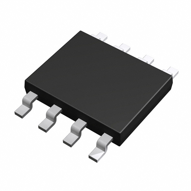
| 描述 | IC EEPROM 32KBIT 20MHZ 8SOP |
| 产品分类 | |
| 品牌 | Rohm Semiconductor |
| 数据手册 | |
| 产品图片 |
|
| 产品型号 | BR25S320F-WE2 |
| rohs | 无铅 / 符合限制有害物质指令(RoHS)规范要求 |
| 产品系列 | - |
| 产品培训模块 | http://www.digikey.cn/PTM/IndividualPTM.page?site=cn&lang=zhs&ptm=30341 |
| 供应商器件封装 | 8-SOP |
| 其它名称 | BR25S320F-WE2CT |
| 包装 | 剪切带 (CT) |
| 存储器类型 | EEPROM |
| 存储容量 | 32K (4K x 8) |
| 封装/外壳 | 8-SOIC(0.173",4.40mm 宽) |
| 工作温度 | -40°C ~ 85°C |
| 接口 | SPI 串行 |
| 标准包装 | 1 |
| 格式-存储器 | EEPROMs - 串行 |
| 电压-电源 | 1.7 V ~ 5.5 V |
| 速度 | 20MHz |


- 商务部:美国ITC正式对集成电路等产品启动337调查
- 曝三星4nm工艺存在良率问题 高通将骁龙8 Gen1或转产台积电
- 太阳诱电将投资9.5亿元在常州建新厂生产MLCC 预计2023年完工
- 英特尔发布欧洲新工厂建设计划 深化IDM 2.0 战略
- 台积电先进制程称霸业界 有大客户加持明年业绩稳了
- 达到5530亿美元!SIA预计今年全球半导体销售额将创下新高
- 英特尔拟将自动驾驶子公司Mobileye上市 估值或超500亿美元
- 三星加码芯片和SET,合并消费电子和移动部门,撤换高东真等 CEO
- 三星电子宣布重大人事变动 还合并消费电子和移动部门
- 海关总署:前11个月进口集成电路产品价值2.52万亿元 增长14.8%


PDF Datasheet 数据手册内容提取
Datasheet Serial EEPROM Series Standard EEPROM SPI BUS EEPROM BR25Sxxx-W Series (32K 64K 128K 256K) ●General Description BR25Sxxx-W series is a serial EEPROM of SPI BUS interface method ●Features ●Packages W(Typ.) x D(Typ.) x H(Max.) (cid:132) High speed clock action up to 20MHz (Max.) (cid:132) Wait function by HOLDB terminal (cid:132) Part or whole of memory arrays settable as read only memory area by program (cid:132) 1.7V to 5.5V single power source action most suitable for battery use SOP8 TSSOP-B8 (cid:132) Page write mode useful for initial value write at 5 .00mm x 6.20mm x 1.71mm 3.00mm x 6.40mm x 1.20mm factory shipment (cid:132) Highly reliable connection by Au pad and Au wire (cid:132) For SPI bus interface (CPOL, CPHA) = (0, 0), (1, 1) (cid:132) Auto erase and auto end function at data rewrite (cid:132) Low current consumption (cid:190) At write action (5V) : 1.5mA (Typ.) SOP-J8 TSSOP-B8J (cid:190) At read action (5V) : 1.0mA (Typ.) 4.90mm x 6.00mm x 1.65mm 3.00mm x 4.90mm x 1.10mm (cid:190) At standby action (5V) : 0.1μA (Typ.) (cid:132) Address auto increment function at read action (cid:132) Write mistake prevention function (cid:190) Write prohibition at power on (cid:190) Write prohibition by command code (WRDI) SSOP-B8 MSOP8 (cid:190) Write prohibition by WP pin 3.00mm x 6.40mm x 1.35mm 2.90mm x 4.00mm x 0.90mm (cid:190) Write prohibition block setting by status registers (BP1, BP0) (cid:190) Write mistake prevention function at low voltage (cid:132) Data kept for 40 years (cid:132) Data rewrite up to 1,000,000 times VSON008X2030 (cid:132) Data at shipment 2.00mm x 3.00mm x 0.60mm Memory array: FFh Status register: WPEN, BP1, BP0 : 0 ●Page write Page 32Byte 64Byte BR25S320-W BR25S128-W Part Number BR25S640-W BR25S256-W ●BR25Sxxx-W Series Power source VSON008 Capacity Bit format SOP8 SOP-J8 SSOP-B8 TSSOP-B8 MSOP8 TSSOP-B8J voltage X2030 32Kbit 4K×8 1.7V to 5.5V ● ● ● ● ● ● ● 64Kbit 8K×8 1.7V to 5.5V ● ● ● ● ● ● 128Kbit 16K×8 1.7V to 5.5V ● ● ● ● 256Kbit 32K×8 1.7V to 5.5V ● ● ○Product structure:Silicon monolithic integrated circuit ○This product is not designed protection against radioactive rays www.rohm.com TSZ02201-0R2R0G100330-1-2 ©2012 ROHM Co., Ltd. All rights reserved. 1/31 TSZ22111・14・001 21.AUG.2012 Rev.001
BR25Sxxx-W Series (32K 64K 128K 256K) Datasheet ●Absolute Maximum Ratings (Ta=25℃) Parameter Symbol Ratings Unit Remarks Supply Voltage V -0.3 to +6.5 V CC 450 (SOP8) When using at Ta=25℃ or higher 4.5mW to be reduced per 1℃. 450 (SOP-J8) When using at Ta=25℃ or higher 4.5mW to be reduced per 1℃. 300 (SSOP-B8) When using at Ta=25℃ or higher 3.0mW to be reduced per 1℃. Power Dissipation Pd 330 (TSSOP-B8) mW When using at Ta=25℃ or higher 3.3mW to be reduced per 1℃. 310 (TSSOP-B8J) When using at Ta=25℃ or higher 3.1mW to be reduced per 1℃. 310 (MSOP8) When using at Ta=25℃ or higher 3.1mW to be reduced per 1℃. 300 (VSON008X2030) When using at Ta=25℃ or higher 3.0mW to be reduced per 1℃. Storage Temperature Tstg -65 to +125 ℃ Operating Temperature Topr -40 to +85 ℃ Terminal Voltage ‐ -0.3 to Vcc+0.3 V ●Memory cell characteristics (Ta=25°C , Vcc=1.7V to 5.5V) Limits Parameter Unit Min. Typ. Max. Number of data rewrite times *1 1,000,000 - - Times Data hold years *1 40 - - Years *1 Not 100% TESTED ●Recommended Operating Ratings Parameter Symbol Ratings Unit Power source voltage Vcc 1.7 to 5.5 V Input voltage V 0 to Vcc IN ●Input / output capacity (Ta=25°C, frequency=5MHz) Parameter Symbol Min. Max. Unit Conditions Input capacity *1 C - 8 V =GND IN pF IN Output capacity *1 C - 8 V =GND OUT OUT *1 Not 100% TESTED. ●Electrical characteristics (Unless otherwise specified, Ta=-40°C to +85°C, Vcc=1.7V to 5.5V) Limits Parameter Symbol Unit Conditions Min. Typ. Max. “H” Input Voltage1 VIH1 0.7xVcc - Vcc+0.3 V 1.7≦Vcc≦5.5V “L” Input Voltage1 VIL1 -0.3 - 0.3xVcc V 1.7≦Vcc≦5.5V “L” Output Voltage1 VOL1 0 - 0.4 V IOL=2.1mA, 2.5≦Vcc<5.5V “L” Output Voltage2 VOL2 0 - 0.2 V IOL=1.0mA, 1.7≦Vcc<2.5V “H” Output Voltage1 VOH1 Vcc-0.2 - Vcc V IOH=-0.4mA, 2.5V≦Vcc<5.5V “H” Output Voltage2 VOH2 Vcc-0.2 - Vcc V IOH=-100µA, 1.7≦Vcc<2.5V Input Leakage Current ILI -1 - 1 μA V =0 to Vcc IN Output Leakage Current ILO -1 - 1 μA V =0 to Vcc, CSB=Vcc OUT 0.5 *1 Vcc=1.8V, fSCK=5MHz, tE/W=5ms ICC1 - - mA 1 *2 Byte Write, Page Write, Write Status register 1 *1 Vcc=2.5V, fSCK=10MHz, tE/W=5ms Operating Current Write ICC2 - - mA 1.5 *2 Byte Write, Page Write, Write Status register 2 *1 Vcc=5.5V, fSCK=20MHz, tE/W=5ms ICC3 - - mA 3 *2 Byte Write, Page Write, Write Status register Vcc=1.8V, fSCK=5MHz, SO=OPEN ICC4 - - 1 mA Read, Read Status Register Vcc=2.5V, fSCK=2MHz, SO=OPEN ICC5 - - 1 mA Read, Read Status Register Vcc=2.5V, fSCK=5MHz, SO=OPEN ICC6 - - 1.5 mA Read, Read Status Register Vcc=2.5V, fSCK=10MHz, SO=OPEN Operating Current Read ICC7 - - 2 mA Read, Read Status Register Vcc=5.5V, fSCK=5MHz, SO=OPEN ICC8 - - 2 mA Read, Read Status Register Vcc=5.5V, fSCK=10MHz, SO=OPEN ICC9 - - 4 mA Read, Read Status Register Vcc=5.5V, fSCK=20MHz, SO=OPEN ICC10 - - 8 mA Read, Read Status Register Vcc=5.5V, SO=OPEN Standby Current ISB - - 2 μA CSB=HOLDB=WP=Vcc, SCK=SI=Vcc or GND *1 BR25S320/640-W *2 BR25S128/256-W www.rohm.com TSZ02201-0R2R0G100330-1-2 ©2012 ROHM Co., Ltd. All rights reserved. 2/31 TSZ22111・15・001 21.AUG.2012 Rev.001
BR25Sxxx-W Series (32K 64K 128K 256K) Datasheet ●Operating timing characteristics (Ta=-40°C to +85°C, unless otherwise specified, load capacity C =30pF) L 1.7≦Vcc<2.5V 1.8≦Vcc<2.5V 2.5≦Vcc<4.5V 4.5≦Vcc<5.5V Parameter Symbol Unit Min. Typ. Max. Min. Typ. Max. Min. Typ. Max. Min. Typ. Max. SCK frequency fSCK - - 3 - - 5 - - 10 - - 20 MHz SCK high time tSCKWH 125 - - 80 - - 40 - - 20 - - ns SCK low time tSCKWL 125 - - 80 - - 40 - - 20 - - ns CSB high time tCS 250 - - 90 - - 40 - - 20 - - ns CSB setup time tCSS 100 - - 60 - - 30 - - 15 - - ns CSB hold time tCSH 100 - - 60 - - 30 - - 15 - - ns SCK setup time tSCKS 100 - - 50 - - 20 - - 15 - - ns SCK hold time tSCKH 100 - - 50 - - 20 - - 15 - - ns SI setup time tDIS 30 - - 20 - - 10 - - 5 - - ns SI hold time tDIH 50 - - 20 - - 10 - - 5 - - ns Data output delay time tPD - - 125 - - 80 - - 40 - - 20 ns Output hold time tOH 0 - - 0 - - 0 - - 0 - - ns Output disable time tOZ - - 200 - - 80 - - 40 - - 20 ns HOLDB setting setup time tHFS 100 - - 0 - - 0 - - 0 - - ns HOLDB setting hold time tHFH 100 - - 20 - - 10 - - 5 - - ns HOLDB release setup time tHRS 100 - - 0 - - 0 - - 0 - - ns HOLDB release hold time tHRH 100 - - 20 - - 10 - - 5 - - ns Time from HOLDB to output High-Z tHOZ - - 100 - - 80 - - 40 - - 20 ns Time from HOLDB to output change tHPD - - 100 - - 80 - - 40 - - 20 ns *1 SCK rise time tRC - - 1 - - 1 - - 1 - - 1 μs *1 SCK fall time tFC - - 1 - - 1 - - 1 - - 1 μs *1 OUTPUT rise time tRO - - 100 - - 50 - - 40 - - 20 ns *1 OUTPUT fall time tFO - - 100 - - 50 - - 40 - - 20 ns Write time tE/W - - 5 - - 5 - - 5 - - 5 ms *1 NOT 100% TESTED ●AC timing characteristics conditions Limits Parameter Symbol Unit Min. Typ. Max. Load capacity C - - 30 pF L Input rise time - - - 50 ns Input fall time - - - 50 ns Input voltage - 0.2Vcc/0.8Vcc V Input / Output judgment voltage - 0.3Vcc/0.7Vcc V ●Sync data input / output timing tCS tCSS tCS CSB tSCKS tSCKWL tSCKWH tRC tFC CSB tCSH tSCKH S CK tDIS tDIH SCK SSOI High-Z SSOI tPD tOH tRO,tFO tOZ High-Z Figure 1. Input timing Figure 2. Input / Output timing SI is taken into IC inside in sync with data rise edge of SO is output in sync with data fall edge of SCK. Data is SCK. Input address and data from the most significant bit output from the most significant bit MSB. MSB CSB "H" "L" tHFS tHFH tHRStHRH SCK tDIS SI n+1 n n-1 SO Dn+1 tDHnOZ High-Z tHPD Dn Dn-1 HOLDB Figure 3. HOLD timing www.rohm.com TSZ02201-0R2R0G100330-1-2 ©2012 ROHM Co., Ltd. All rights reserved. 3/31 TSZ22111・15・001 21.AUG.2012 Rev.001
BR25Sxxx-W Series (32K 64K 128K 256K) Datasheet ●Block Diagram CSB 1 VOLTAGE 8 Vcc INSTRUCTION DECODE DETECTION CONTROL CLOCK GENERATION WRITE HIGH VOLTAGE SO 2 INHIBITION GENERATOR 7 HOLDB INSTRUCTION REGISTER STATUS REGISTER WP 3 ADDRESS 12to15bit*1 ADDRESS 12to15bit *1 6 SCK REGISTER DECODER 32to256K EEPROM *1 12bit: BR25S320-W GND 4 DREAGTAIS TER 8bit REAADM/WP RITE 8bit 5 SI 1134bbiitt:: BBRR2255SS614208--WW 15bit: BR25S256-W ●Pin Configuration (TOP VIEW) Vcc HOLDB SCK SI BR25S320-W BR25S640-W BR25S128-W BR25S256-W CSB SO WP GND ●Pin Descriptions Terminal Input Function name /Output Vcc - Power source to be connected GND - All input / output reference voltage, 0V CSB Input Chip select input SCK Input Serial clock input SI Input Start bit, ope code, address, and serial data input SO Output Serial data output Hold input HOLDB Input Command communications may be suspended temporarily (HOLD status) Write protect input WP Input Write command is prohibited Write status register command is prohibited www.rohm.com TSZ02201-0R2R0G100330-1-2 ©2012 ROHM Co., Ltd. All rights reserved. 4/31 TSZ22111・15・001 21.AUG.2012 Rev.001
BR25Sxxx-W Series (32K 64K 128K 256K) Datasheet ●Typical Performance Curves (The following characteristic data are Typ. Values.) Figure 4. "H" Input Voltage VIH Figure 5. "L" Input VoltageVIL (CSB,SCK,SI,HOLDB,WP) (CSB,SCK,SI,HOLDB,WP) Figure 6. "L" Output Voltage VOL1(Vcc=2.5V) Figure 7."H" Output Voltage VOH1 (Vcc=2.5V) www.rohm.com TSZ02201-0R2R0G100330-1-2 ©2012 ROHM Co., Ltd. All rights reserved. 5/31 TSZ22111・15・001 21.AUG.2012 Rev.001
BR25Sxxx-W Series (32K 64K 128K 256K) Datasheet ●Typical Performance Curves‐Continued Figure 8. Input Leak Current ILI Figure 9.Output Leak Current ILO (SO) (CSB,SCK,SI,HOLDB,WP) Figure 10. Current consumption at WRITE operationICC3 Figure 11.Current consumption at WRITE operation ICC3 (BR25S320/640-W) (BR25S128/256-W) www.rohm.com TSZ02201-0R2R0G100330-1-2 ©2012 ROHM Co., Ltd. All rights reserved. 6/31 TSZ22111・15・001 21.AUG.2012 Rev.001
BR25Sxxx-W Series (32K 64K 128K 256K) Datasheet ●Typical Performance Curves‐Continued Figure 12. Current consumption at READ operationICC10 Figure 13.Current consumption at standby operationISB Figure 14. SCK frequency fSCK Figure 15.SCK high time tSCKWH www.rohm.com TSZ02201-0R2R0G100330-1-2 ©2012 ROHM Co., Ltd. All rights reserved. 7/31 TSZ22111・15・001 21.AUG.2012 Rev.001
BR25Sxxx-W Series (32K 64K 128K 256K) Datasheet ●Typical Performance Curves‐Continued Figure 16. SCK low time tSCKWL Figure 17. CSB high time tCS Figure 18. CSB setup time tCSS Figure 19.CSB hold time tCSH www.rohm.com TSZ02201-0R2R0G100330-1-2 ©2012 ROHM Co., Ltd. All rights reserved. 8/31 TSZ22111・15・001 21.AUG.2012 Rev.001
BR25Sxxx-W Series (32K 64K 128K 256K) Datasheet ●Typical Performance Curves‐Continued Figure 20. SI setup time tDIS Figure 21. SI hold time tDIH Figure 22. Data output delay time tPD Figure 23.Output disable time tOZ www.rohm.com TSZ02201-0R2R0G100330-1-2 ©2012 ROHM Co., Ltd. All rights reserved. 9/31 TSZ22111・15・001 21.AUG.2012 Rev.001
BR25Sxxx-W Series (32K 64K 128K 256K) Datasheet ●Typical Performance Curves‐Continued Figure 24. HOLDB setting hold time tHFH Figure 25.HOLDB release hold time tHRH Figure 26. Time from HOLDB to output High-Z tHOZ Figure 27.Time from HOLDB to output change tHPD www.rohm.com TSZ02201-0R2R0G100330-1-2 ©2012 ROHM Co., Ltd. All rights reserved. 10/31 TSZ22111・15・001 21.AUG.2012 Rev.001
BR25Sxxx-W Series (32K 64K 128K 256K) Datasheet ●Typical Performance Curves‐Continued Figure 28. Output rise time tRO Figure 29. Output fall time tFO Figure 30. Write cycle time tE/W www.rohm.com TSZ02201-0R2R0G100330-1-2 ©2012 ROHM Co., Ltd. All rights reserved. 11/31 TSZ22111・15・001 21.AUG.2012 Rev.001
BR25Sxxx-W Series (32K 64K 128K 256K) Datasheet ●Features ○Status registers This IC has status register. The status register expresses the following parameters of 8 bits. BP0 and BP1 can be set by write status register command. These 2 bits are memorized into the EEPROM, therefore are valid even when power source is turned off. Rewrite characteristics and data hold time are same as characteristics of the EEPROM. WEN can be set by write enable command and write disable command. WEN becomes write disable status when power source is turned off. R/B is for write confirmation, therefore cannot be set externally. The value of status register can be read by read status register command. 1. Contexture of status register Product number bit 7 bit 6 bit 5 bit 4 bit 3 bit 2 bit 1 bit 0 BR25S320-W BR25S640-W ― WPEN 0 0 0 BP1 BP0 WEN R/B BR25S128-W BR25S256-W Memory bit Function location WP pin enable / disable designation bit WPEN EEPROM WPEN=0=invalid WPEN=1=valid BP1 EEPROM EEPROM write disable block designation bit BP0 Write and write status register write enable / disable status confirmation bit WEN registers WEN=0=prohibited WEN=1=permitted Write cycle status (READY / BUSY) status confirmation bit R―/B registers R―/B=0=READY ― R/B=1=BUSY 2. Write disable block setting Write disable block BP1 BP0 BR25S320-W BR25S640-W BR25S128-W BR25S256-W 0 0 None None None None 0 1 C00h-FFFh 1800h-1FFFh 3000h-3FFFh 6000h-7FFFh 1 0 800h-FFFh 1000h-1FFFh 2000h-3FFFh 4000h-7FFFh 1 1 000h-FFFh 0000h-1FFFh 0000h-3FFFh 0000h-7FFFh ○WP pin By setting WP=LOW, write command is prohibited. And the write command to be disabled at this moment is WRSR. However, when write cycle is in execution, no interruption can be made. Product number WRSR WRITE BR25S320-W BR25S640-W Prohibition possible Prohibition BR25S128-W but WPEN bit “1” impossible BR25S256-W ○HOLDB pin By HOLDB pin, data transfer can be interrupted. When SCK=”0”, by making HOLDB from “1” into”0”, data transfer to EEPROM is interrupted. When SCK = “0”, by making HOLDB from “0” into “1”, data transfer is restarted. www.rohm.com TSZ02201-0R2R0G100330-1-2 ©2012 ROHM Co., Ltd. All rights reserved. 12/31 TSZ22111・15・001 21.AUG.2012 Rev.001
BR25Sxxx-W Series (32K 64K 128K 256K) Datasheet ●Command mode Command Contents Ope code WREN Write enable command 0000 0110 WRDI Write disable command 0000 0100 READ Read command 0000 0011 WRITE Write command 0000 0010 RDSR Read status register command 0000 0101 WRSR Write status register command 0000 0001 ●Timing chart 1. Write enable (WREN) / disable (WRDI) command WREN (WRITE ENABLE): Write enable WRDI (WRITE DISABLE): Write disable CSB CSB SCK 0 1 2 3 4 5 6 7 SCK 0 1 2 3 4 5 6 7 SI 0 0 0 0 0 1 1 0 SI 0 0 0 0 0 1 0 0 SO High-Z SO High-Z Figure 31. Write enable command Figure 32. Write disable command This IC has write enable status and write disable status. It is set to write enable status by write enable command, and it is set to write disable status by write disable command. As for these commands, set CSB LOW, and then input the respective ope codes. The respective commands are accepted at the 7-th clock rise. Even with input over 7 clocks, command becomes valid. When to carry out write command, it is necessary to set write enable status by the write enable command. If write command is input in the write disable status, the command is cancelled. And even in the write enable status, once write command is executed, it gets in the write disable status. After power on, this IC is in write disable status. 2. Read command (READ) Product Address CSB number length ~~ ~~ BR25S320-W A11-A0 SCK 0 1 2 3 4 5 6 7 8 9 10 11 ~~ 23 24 ~~ 3300 31 BR25S640-W A12-A0 SI 0 0 0 0 0 0 1 1 * A14 A13 A12 ~~ A1 A0 BR25S128-W A13-A0 ~~ ~~ BR25S256-W A14-A0 SO High-Z ~~ D7 D6 ~~~~ D2 D1 D0 Figure 33. Read command By read command, data of EEPROM can be read. As for this command, set CSB LOW, then input address after read ope code. EEPROM starts data output of the designated address. Data output is started from SCK fall of 23-th clock, and from D7 to D0 sequentially. This IC has increment read function. After output of data for 1 byte (8bits), by continuing input of SCK, data of the next address can be read. Increment read can read all the addresses of EEPROM. After reading data of the most significant address, by continuing increment read, data of the most insignificant address is read. www.rohm.com TSZ02201-0R2R0G100330-1-2 ©2012 ROHM Co., Ltd. All rights reserved. 13/31 TSZ22111・15・001 21.AUG.2012 Rev.001
BR25Sxxx-W Series (32K 64K 128K 256K) Datasheet 3. Write command (WRITE) Product Address C SB ~~ ~~ number length SCK 0 1 2 3 4 5 6 7 8 9 10 11 23 24 ~~ 30 31 BR25S320-W A11-A0 ~~ ~~ ~~ BR25S640-W A12-A0 SI 0 0 0 0 0 0 1 0 * A14 A13 A12 ~~ A1 A0 D7 D6 ~~ D2 D1 D0 BR25S128-W A13-A0 SO High-Z ~~ BR25S256-W A14-A0 *=Don't Care Figure 34. Write command By write command, data of EEPROM can be written. As for this command, set CSB LOW, then input address and data after write ope code. Then, by making CSB HIGH, the EEPROM starts writing. The write time of EEPROM requires time of tE/W (Max 5ms). During tE/W, other than read status register command is not accepted. Set CSB HIGH between taking the last data (D0) and rising the next SCK clock. At the other timing, write command is not executed, and this write command is cancelled. This IC has page write function, and after input of data for 1 byte (8 bits), by continuing data input without setting CSB HIGH, 2byte or more data can be written for one tE/W. The maximum number of write bytes is specified per device of each capacity. Up to 64 arbitrary bytes can be written (in the case of BR25S128/256-W). In page write, the insignificant 5 bit of the designated address is incremented internally at every time when data of 1 byte is input and data is written to respective addresses. When data of the maximum bytes or higher is input, address rolls over, and previously input data is overwritten. 4. Write status register, Read status register command (WRSR/RDSR) CSB SCK 0 1 2 3 4 5 6 7 8 9 10 11 12 13 14 15 bit7 bit6 bit5 bit4 bit3 bit2 bit1 bit0 SI 0 0 0 0 0 0 0 1 WPE N * * * BP1 BP0 * * SO High-Z *=Don't care Figure 35. Write status register Write status register command can write data of status register. The data can be written by this command are 3 bits, that is, WPEN(bit7), BP1 (bit3) and BP0 (bit2) among 8 bits of status register. By BP1 and BP0, write disable block of EEPROM can be set. As for this command, set CSB LOW, and input ope code of write status register, and input data. Then, by making CSB HIGH, EEPROM starts writing. Write time requires time of tE/W as same as write. As for CSB rise, set CSB HIGH between taking the last data bit (bit0) and the next SCK clock rising. At the other timing, command is cancelled. Write disable block is determined by BP1 BP0, and the block can be selected from 1/4 , 1/2, and entire of memory array (Refer to the write disable block setting table.). To the write disabled block, write cannot be made, and only read can be made. CSB SCK 0 1 2 3 4 5 6 7 8 9 10 11 12 13 14 15 SI 0 0 0 0 0 1 0 1 SO High-Z WbPit7EN bi0t6 bi0t5 bi0t4 BbiPt31 BbiPt20 WbiEt1N Rbi/tB0 Figure 36. Read status register command www.rohm.com TSZ02201-0R2R0G100330-1-2 ©2012 ROHM Co., Ltd. All rights reserved. 14/31 TSZ22111・15・001 21.AUG.2012 Rev.001
BR25Sxxx-W Series (32K 64K 128K 256K) Datasheet ●WP cancel valid area WP is normally fixed to “H” or “L” for use, but when WP is controlled so as to cancel write status register command, pay attention to the following WP valid timing. While write status register command is executed, by setting WP = “L” in cancel valid area, command can be cancelled. The area from command ope code to CSB rise at internal automatic write start becomes the cancel valid area. However, once write is started, by any input write cycle cannot be cancelled. WP input becomes Don’t Care, and cancellation becomes invalid. SCK 6 7 15 16 Ope Code Data Data twEr/iWte time Valid Invalid (WRSR command is reset by WPB=L) Figure 37. WP valid timing (At inputting WRSR command) ●HOLDB pin By HOLDB pin, command communication can be stopped temporarily (HOLD status). The command communications are carried out when the HOLDB pin is HIGH. To get in HOLD status, at command communication, when SCK=LOW, set the HOLDB pin LOW. At HOLD status, SCK and SI become Don’t Care, and SO becomes high impedance (High-Z). To release the HOLD status, set the HOLDB pin HIGH when SCK=LOW. After that, communication can be restarted from the point before the HOLD status. For example, when HOLD status is made after A5 address input at read, after release of HOLD status, by starting A4 address input, read can be restarted. When in HOLD status, keep CSB LOW. When it is set CSB=HIGH in HOLD status, the IC is reset, therefore communication after that cannot be restarted. www.rohm.com TSZ02201-0R2R0G100330-1-2 ©2012 ROHM Co., Ltd. All rights reserved. 15/31 TSZ22111・15・001 21.AUG.2012 Rev.001
BR25Sxxx-W Series (32K 64K 128K 256K) Datasheet ●Method to cancel each command ○READ, RDSR ・Method to cancel : cancel by CSB = “H”. Ope code Address Data Ope code Data 8 bits 16 bits 8 bits 8 bits 8 bits Cancel available in all areas of read mode Cancel available in all areas of rdsr mode Figure 38. READ cancel valid timing Figure 39. RDSR cancel valid timing ○WRITE、PAGE WRITE Ope code Address Data tE/W a :Ope code or address input area Cancellation is available by CSB=”H”. 8bits 16bits 8bits a b d b :Data input area (D7 to D1 input area) Cancellation is available by CSB=”H”. c c:Data input area (D0 area) In this area, cancellation is not available. SCK When CSB is set HIGH, write starts. d :tE/W area SI D7 D6 D5 D4 D3 D2 D1 D0 In the area c, by rising CSB, write starts. b c While writing, by any input, cancellation cannot be made. Figure 40. WRITE cancel valid timing Note1) If Vcc is made OFF during write execution, designated address data is not guaranteed, therefore write it once again. Note2) If CSB is rised at the same timing as that of the SCK rise, write execution / cancel becomes unstable, therefore, it is recommended to rise in SCK = “L” area. As for SCK rise, assure timing of tCSS / tCSH or more. ○WRSR a :From ope code to 15-th clock rise SCK 14 15 16 17 Cancellation is available by CSB=”H”. b :From 15-th clock rise to 16-th clock rise (write enable area) SI D1 D0 In this area, cancellation is not available. a b c When CSB is set HIGH, write starts. c:After 16-th clock rise. Ope code Data tE/W Cancellation is available by CSB=”H”. 8 bits 8 bits However, if write starts (CSB is rised) a c in the area b, cancellation cannot be made by any means. b And, by inputting on SCK clock, cancellation cannot be made. Figure 41. WRSR cancel valid timing Note1) If Vcc is made OFF during write execution, designated address data is not guaranteed, therefore write it once again Note2) If CSB is rised at the same timing as that of the SCK rise, write execution / cancel becomes unstable, therefore, it is recommended to rise in SCK = “L” area. As for SCK rise, assure timing of tCSS / tCSH or more. ○WREN/WRDI SCK 6 7 8 a :From ope code to 7-th clock rise, cancellation is available by CSB = “H”. b :Cancellation is not available 7-th clock. Ope code 8 bits a b Figure 42. WREN/WRDI cancel valid timing www.rohm.com TSZ02201-0R2R0G100330-1-2 ©2012 ROHM Co., Ltd. All rights reserved. 16/31 TSZ22111・15・001 21.AUG.2012 Rev.001
BR25Sxxx-W Series (32K 64K 128K 256K) Datasheet ●I/O peripheral circuits In order to realize stable high speed operations, pay attention to the following input / output pin conditions. ○Input pin pull up, pull down resistance When to attach pull up, pull down resistance to EEPROM input pin, select an appropriate value for the microcontroller VOL, IOL with considering VIL characteristics of this IC. V -V 1. Pull up resistance R ≧ CC OLM ・・・① PU IOLM V ≦ V ・・・② OLM ILE Microcontroller IOLM RPU EEPROM Example) When Vcc=5V, VILE=1.5V, VOLM=0.4V, IOLM=2mA, VOLM VILE from the equation ①, 5-0.4 “L” output “L” input RPU≧ 2×10⁻³ ∴R ≧ 2.3[kΩ] PU Figure 43. Pull up resistance With the value of Rpu to satisfy the above equation, VOLM becomes 0.4V or lower, and with VILE (=1.5V), the equation ② is also satisfied. ・V :EEPROM V specifications ILE IL ・V :Microcontroller V specifications OLM OL ・I :Microcontroller I specifications OLM OL And, in order to prevent malfunction or erroneous write at power ON/OFF, be sure to make CSB pull up. V OHM 2.Pull down resistance R ≧ ・・・③ PD I OHM Microcontroller EEPROM VOHM≧ V IHE ・・・④ VOHM VIHE Example) When VCC=5V, VOHM=VCC-0.5V, IOHM=0.4mA, V =V ×0.7V, from the equation③, IHE CC “H” output IOHM RPD “H” input RPD≧ 05.4-×01.05-3 Figure 44. Pull down resistance ∴RPD≧ 11.3[k Ω] Further, by amplitude VIHE, VILE of signal input to EEPROM, operation speed changes. By inputting Vcc/GND level amplitude of signal, more stable high speed operations can be realized. On the contrary, when amplitude of 0.8VCC / 0.2Vcc is input, operation speed becomes slow.*1 In order to realize more stable high speed operation, it is recommended to make the values of R , R as large as PU PD possible, and make the amplitude of signal input to EEPROM close to the amplitude of VCC / GND level. (*1 In this case, guaranteed value of operating timing is guaranteed.) ○SO load capacity condition Load capacity of SO output pin affects upon delay characteristic of SO output (Data output delay time, time from HOLDB to High-Z, Output rise time, Output fall time.). In order to make output delay characteristic into better, make SO load capacity small. EEPROM SO CL Figure 45. SO load capacity ○Other cautions Make the each wire length from the microcontroller to EEPROM input pin same length, in order to prevent setup / hold violation to EEPROM, owing to difference of wire length of each input. www.rohm.com TSZ02201-0R2R0G100330-1-2 ©2012 ROHM Co., Ltd. All rights reserved. 17/31 TSZ22111・15・001 21.AUG.2012 Rev.001
BR25Sxxx-W Series (32K 64K 128K 256K) Datasheet ●Equivalent circuit ○Output circuit internal signal SO internal signal Figure 46. SO output equivalent circuit ○Input circuit internal CSB signal internal signal Figure 47. CSB input equivalent circuit SCK isnigtenranla l SI isnigtenranla l Figure 48. SCK input equivalent circuit Figure 49. SI input equivalent circuit HOLDB isnigtenranla l WP isnigtenranla l Figure 50. HOLDB input equivalent circuit Figure 51. WP input equivalent circuit www.rohm.com TSZ02201-0R2R0G100330-1-2 ©2012 ROHM Co., Ltd. All rights reserved. 18/31 TSZ22111・15・001 21.AUG.2012 Rev.001
BR25Sxxx-W Series (32K 64K 128K 256K) Datasheet ●Notes on power ON/OFF ○At standby Set CSB “H”, and be sure to set SCK, SI input “L” or “H”. Do not input intermediate electric potantial. ○At power ON/OFF When Vcc rise or fall, set CSB=”H” (=Vcc). When CSB is “L”, this IC gets in input accept status (active). If power is turned on in this status, noises and the likes may cause malfunction, erroneous write or so. To prevent these, at power ON, set CSB “H”. (When CSB is in “H” status, all inputs are canceled.) Vcc CSB Good example Bad example Figure 52. CSB timing at power ON/OFF (Good example) CSB terminal is pulled up to Vcc. At power OFF, take 10ms or more before supply. If power is turned on without observing this condition, the IC internal circuit may not be reset. (Bad example) CSB terminal is “L” at power ON/OFF. In this case, CSB always becomes “L” (active status), and EEPROM may have malfunction or erroneous write owing to noises and the likes. Even when CSB input is High-Z, the status becomes like this case. ○Operating timing after power ON As shown in Figure 53, at standby, when SCK is “H”, even if CSB is fallen, SI status is not read at fall edge. SI status is read at SCK rise edge after fall of CSB. At standby and at power ON/OFF, set CSB “H” status. Even if CSB is fallen at SCK=”H”, SI status is not read at that edge. CSB Command start here. SI is read. SCK 0 1 2 SI Figure 53. Operating timing ○At power on malfunction preventing function This IC has a POR (Power On Reset) circuit as mistake write countermeasure. After POR action, it gets in write disable status. The POR circuit is valid only when power is ON, and does not work when power is OFF. When power is ON, if the recommended conditions of the following tR, tOFF, and Vbot are not satisfied, it may become write enable status owing to noises and the likes. tR Vcc Recommended conditions of tR, tOFF, Vbot tR tOFF Vbot tOFF 10ms or below 10ms or higher 0.3V or below Vbot 0 100ms or below 10ms or higher 0.2V or below Figure 54. Rise waveform ○Low voltage malfunction preventing function LVCC (Vcc-Lockout) circuit prevents data rewrite action at low power, and prevents wrong write. At LVCC voltage (Typ. =1.2V) or below, it prevent data rewrite. www.rohm.com TSZ02201-0R2R0G100330-1-2 ©2012 ROHM Co., Ltd. All rights reserved. 19/31 TSZ22111・15・001 21.AUG.2012 Rev.001
BR25Sxxx-W Series (32K 64K 128K 256K) Datasheet ●Noise countermeasures ○Vcc noise (bypass capacitor) When noise or surge gets in the power source line, malfunction may occur, therefore, for removing these, it is recommended to attach a bypass capacitor (0.1μF) between IC Vcc and GND. At that time, attach it as close to IC as possible. And, it is also recommended to attach a bypass capacitor between board Vcc and GND. ○SCK noise When the rise time of SCK (tRC) is long, and a certain degree or more of noise exists, malfunction may occur owing to clock bit displacement. To avoid this, a Schmitt trigger circuit is built in SCK input. The hysteresis width of this circuit is set about 0.2V, if noises exist at SCK input, set the noise amplitude 0.2Vp-p or below. And it is recommended to set the rise time of SCK (tRC) 100ns or below. In the case when the rise time is 100ns or higher, take sufficient noise countermeasures. Make the clock rise, fall time as small as possible. ○WP noise During execution of write status register command, if there exist noises on WP pin, mistake in recognition may occur and forcible cancellation may result. To avoid this, a Schmitt trigger circuit is built in WP input. In the same manner, a Schmitt trigger circuit is built in CSB input, SI input and HOLDB input too. ●Notes for use (1) Described numeric values and data are design representative values, and the values are not guaranteed. (2) We believe that application circuit examples are recommendable, however, in actual use, confirm characteristics further sufficiently. In the case of use by changing the fixed number of external parts, make your decision with sufficient margin in consideration of static characteristics and transition characteristics and fluctuations of external parts and our LSI. (3) Absolute maximum ratings If the absolute maximum ratings such as impressed voltage and operating temperature range and so forth are exceeded, LSI may be destructed. Do not impress voltage and temperature exceeding the absolute maximum ratings. In the case of fear exceeding the absolute maximum ratings, take physical safety countermeasures such as fuses, and see to it that conditions exceeding the absolute maximum ratings should not be impressed to LSI. (4) GND electric potential Set the voltage of GND terminal lowest at any action condition. Make sure that each terminal voltage is higher than that of GND terminal. (5) Heat design In consideration of permissible dissipation in actual use condition, carry out heat design with sufficient margin. (6) Terminal to terminal short circuit and wrong packaging When to package LSI onto a board, pay sufficient attention to LSI direction and displacement. Wrong packaging may destruct LSI. And in the case of short circuit between LSI terminals and terminals and power source, terminal and GND owing to foreign matter, LSI may be destructed. (7) Use in a strong electromagnetic field may cause malfunction, therefore, evaluate design sufficiently. Status of this document The Japanese version of this document is formal specification. A customer may use this translation version only for a reference to help reading the formal version. If there are any differences in translation version of this document formal version takes priority. www.rohm.com TSZ02201-0R2R0G100330-1-2 ©2012 ROHM Co., Ltd. All rights reserved. 20/31 TSZ22111・15・001 21.AUG.2012 Rev.001
BR25Sxxx-W Series (32K 64K 128K 256K) Datasheet ●Ordering Information Product Code Description B R 2 5 S x x x x x x - W x x BUS type 25:SPI Operating temperature -40℃ to+85℃ Capacity 32=32K 256=256K 64=64K 128=128K Package F :SOP8 FJ :SOP-J8 FV : SSOP-B8 FVT : TSSOP-B8 FVJ : TSSOP-B8J FVM : MSOP8 NUX : VSON008X2030 Double Cell Packaging and forming specification E2 : Embossed tape and reel (SOP8,SOP-J8, SSOP-B8,TSSOP-B8, TSSOP-B8J) TR : Embossed tape and reel (MSOP8, VSON008X2030) ●Lineup Package Capacity Type Quantity SOP8 SOP-J8 Reel of 2500 SSOP-B8 32K TSSOP-B8 Reel of 3000 TSSOP-B8J Reel of 2500 MSOP8 Reel of 3000 VSON008X2030 Reel of 4000 SOP8 SOP-J8 Reel of 2500 SSOP-B8 64K TSSOP-B8 Reel of 3000 TSSOP-B8J Reel of 2500 MSOP8 Reel of 3000 SOP8 SOP-J8 Reel of 2500 128K SSOP-B8 TSSOP-B8 Reel of 3000 SOP8 256K Reel of 2500 SOP-J8 www.rohm.com TSZ02201-0R2R0G100330-1-2 ©2012 ROHM Co., Ltd. All rights reserved. 21/31 TSZ22111・15・001 21.AUG.2012 Rev.001
BR25Sxxx-W Series (32K 64K 128K 256K) Datasheet ●Physical Dimension Tape and Reel Information SOP8 <Tape and Reel information> Tape Embossed carrier tape Quantity 2500pcs E2 Direction of feed ( The direction is the 1pin of product is at the upper left when you hold ) reel on the left hand and you pull out the tape on the right hand Direction of feed 1pin Reel ∗ Order quantity needs to be multiple of the minimum quantity. www.rohm.com TSZ02201-0R2R0G100330-1-2 ©2012 ROHM Co., Ltd. All rights reserved. 22/31 TSZ22111・15・001 21.AUG.2012 Rev.001
BR25Sxxx-W Series (32K 64K 128K 256K) Datasheet ●Physical Dimension Tape and Reel Information - continued SOP-J8 <Tape and Reel information> Tape Embossed carrier tape Quantity 2500pcs E2 Direction of feed ( The direction is the 1pin of product is at the upper left when you hold ) reel on the left hand and you pull out the tape on the right hand Direction of feed 1pin Reel ∗ Order quantity needs to be multiple of the minimum quantity. www.rohm.com TSZ02201-0R2R0G100330-1-2 ©2012 ROHM Co., Ltd. All rights reserved. 23/31 TSZ22111・15・001 21.AUG.2012 Rev.001
BR25Sxxx-W Series (32K 64K 128K 256K) Datasheet ●Physical Dimension Tape and Reel Information - continued SSOP-B8 SSOP-B8 3.0±0.2 (MAX 3.35 include BURR) 8 7 6 5 32 .. 00 ±± 44 .. 64 N I M 3 . 0 1 2 3 4 1 0.15±0.1 0. ± 5 S 1 1. 0.1 S 1 +0.06 0. (0.52) 0.65 0.22−0.04 0.08 M (Unit : mm) <Tape and Reel information> Tape Embossed carrier tape Quantity 2500pcs E2 Direction of feed ( The direction is the 1pin of product is at the upper left when you hold ) reel on the left hand and you pull out the tape on the right hand Direction of feed 1pin Reel ∗ Order quantity needs to be multiple of the minimum quantity. www.rohm.com TSZ02201-0R2R0G100330-1-2 ©2012 ROHM Co., Ltd. All rights reserved. 24/31 TSZ22111・15・001 21.AUG.2012 Rev.001
BR25Sxxx-W Series (32K 64K 128K 256K) Datasheet ●Physical Dimension Tape and Reel Information - continued TSSOP-B8 <Tape and Reel information> Tape Embossed carrier tape Quantity 3000pcs E2 Direction ( The direction is the 1pin of product is at the upper left when you hold ) of feed reel on the left hand and you pull out the tape on the right hand Direction of feed 1pin Reel ∗ Order quantity needs to be multiple of the minimum quantity. www.rohm.com TSZ02201-0R2R0G100330-1-2 ©2012 ROHM Co., Ltd. All rights reserved. 25/31 TSZ22111・15・001 21.AUG.2012 Rev.001
BR25Sxxx-W Series (32K 64K 128K 256K) Datasheet ●Physical Dimension Tape and Reel Information - continued TSSOP-B8J <Tape and Reel information> Tape Embossed carrier tape Quantity 2500pcs E2 Direction ( The direction is the 1pin of product is at the upper left when you hold ) of feed reel on the left hand and you pull out the tape on the right hand Direction of feed 1pin Reel ∗ Order quantity needs to be multiple of the minimum quantity. www.rohm.com TSZ02201-0R2R0G100330-1-2 ©2012 ROHM Co., Ltd. All rights reserved. 26/31 TSZ22111・15・001 21.AUG.2012 Rev.001
BR25Sxxx-W Series (32K 64K 128K 256K) Datasheet ●Physical Dimension Tape and Reel Information - continued MSOP8 <Tape and Reel information> Tape Embossed carrier tape Quantity 3000pcs TR Direction of feed ( The direction is the 1pin of product is at the upper right when you hold ) reel on the left hand and you pull out the tape on the right hand 1pin Direction of feed Reel ∗ Order quantity needs to be multiple of the minimum quantity. www.rohm.com TSZ02201-0R2R0G100330-1-2 ©2012 ROHM Co., Ltd. All rights reserved. 27/31 TSZ22111・15・001 21.AUG.2012 Rev.001
BR25Sxxx-W Series (32K 64K 128K 256K) Datasheet ●Physical Dimension Tape and Reel Information - continued VSON008X2030 <Tape and Reel information> Tape Embossed carrier tape Quantity 4000pcs TR Direction of feed ( The direction is the 1pin of product is at the upper right when you hold ) reel on the left hand and you pull out the tape on the right hand 1pin Direction of feed Reel ∗ Order quantity needs to be multiple of the minimum quantity. www.rohm.com TSZ02201-0R2R0G100330-1-2 ©2012 ROHM Co., Ltd. All rights reserved. 28/31 TSZ22111・15・001 21.AUG.2012 Rev.001
BR25Sxxx-W Series (32K 64K 128K 256K) Datasheet ●Marking Diagrams SOP8(TOP VIEW) SOP-J8(TOP VIEW) Part Number Marking Part Number Marking LOT Number LOT Number 1PIN MARK 1PIN MARK SSOP-B8(TOP VIEW) TSSOP-B8(TOP VIEW) Part Number Marking Part Number Marking LOT Number LOT Number 1PIN MARK 1PIN MARK TSSOP-B8J(TOP VIEW) MSOP8(TOP VIEW) Part Number Marking Part Number Marking LOT Number LOT Number 1PIN MARK 1PIN MARK VSON008X2030 (TOP VIEW) Part Number Marking LOT Number 1PIN MARK www.rohm.com TSZ02201-0R2R0G100330-1-2 ©2012 ROHM Co., Ltd. All rights reserved. 29/31 TSZ22111・15・001 21.AUG.2012 Rev.001
BR25Sxxx-W Series (32K 64K 128K 256K) Datasheet ●Marking Information Product Name Capacity Package Type Marking S320 SOP8 S320 SOP-J8 S320 SSOP-B8 32K S320 TSSOP-B8 S320 TSSOP-B8J S320 MSOP8 S320 VSON008X2030 S640 SOP8 S640 SOP-J8 S640 SSOP-B8 64K S640 TSSOP-B8 S640 TSSOP-B8J S640 MSOP8 5S128 SOP8 5S128 SOP-J8 128K S128 SSOP-B8 5S128 TSSOP-B8 5S256 SOP8 256K 5S256 SOP-J8 www.rohm.com TSZ02201-0R2R0G100330-1-2 ©2012 ROHM Co., Ltd. All rights reserved. 30/31 TSZ22111・15・001 21.AUG.2012 Rev.001
BR25Sxxx-W Series (32K 64K 128K 256K) Datasheet ●Revision History Date Revision Changes 21.Aug.2012 001 New Release www.rohm.com TSZ02201-0R2R0G100330-1-2 ©2012 ROHM Co., Ltd. All rights reserved. 31/31 TSZ22111・15・001 21.AUG.2012 Rev.001
DDaattaasshheeeett Notice Precaution on using ROHM Products 1. Our Products are designed and manufactured for application in ordinary electronic equipments (such as AV equipment, OA equipment, telecommunication equipment, home electronic appliances, amusement equipment, etc.). If you intend to use our Products in devices requiring extremely high reliability (such as medical equipment (Note 1), transport equipment, traffic equipment, aircraft/spacecraft, nuclear power controllers, fuel controllers, car equipment including car accessories, safety devices, etc.) and whose malfunction or failure may cause loss of human life, bodily injury or serious damage to property (“Specific Applications”), please consult with the ROHM sales representative in advance. Unless otherwise agreed in writing by ROHM in advance, ROHM shall not be in any way responsible or liable for any damages, expenses or losses incurred by you or third parties arising from the use of any ROHM’s Products for Specific Applications. (Note1) Medical Equipment Classification of the Specific Applications JAPAN USA EU CHINA CLASSⅢ CLASSⅡb CLASSⅢ CLASSⅢ CLASSⅣ CLASSⅢ 2. ROHM designs and manufactures its Products subject to strict quality control system. However, semiconductor products can fail or malfunction at a certain rate. Please be sure to implement, at your own responsibilities, adequate safety measures including but not limited to fail-safe design against the physical injury, damage to any property, which a failure or malfunction of our Products may cause. The following are examples of safety measures: [a] Installation of protection circuits or other protective devices to improve system safety [b] Installation of redundant circuits to reduce the impact of single or multiple circuit failure 3. Our Products are designed and manufactured for use under standard conditions and not under any special or extraordinary environments or conditions, as exemplified below. Accordingly, ROHM shall not be in any way responsible or liable for any damages, expenses or losses arising from the use of any ROHM’s Products under any special or extraordinary environments or conditions. If you intend to use our Products under any special or extraordinary environments or conditions (as exemplified below), your independent verification and confirmation of product performance, reliability, etc, prior to use, must be necessary: [a] Use of our Products in any types of liquid, including water, oils, chemicals, and organic solvents [b] Use of our Products outdoors or in places where the Products are exposed to direct sunlight or dust [c] Use of our Products in places where the Products are exposed to sea wind or corrosive gases, including Cl2, H2S, NH3, SO2, and NO2 [d] Use of our Products in places where the Products are exposed to static electricity or electromagnetic waves [e] Use of our Products in proximity to heat-producing components, plastic cords, or other flammable items [f] Sealing or coating our Products with resin or other coating materials [g] Use of our Products without cleaning residue of flux (even if you use no-clean type fluxes, cleaning residue of flux is recommended); or Washing our Products by using water or water-soluble cleaning agents for cleaning residue after soldering [h] Use of the Products in places subject to dew condensation 4. The Products are not subject to radiation-proof design. 5. Please verify and confirm characteristics of the final or mounted products in using the Products. 6. In particular, if a transient load (a large amount of load applied in a short period of time, such as pulse. is applied, confirmation of performance characteristics after on-board mounting is strongly recommended. Avoid applying power exceeding normal rated power; exceeding the power rating under steady-state loading condition may negatively affect product performance and reliability. 7. De-rate Power Dissipation (Pd) depending on Ambient temperature (Ta). When used in sealed area, confirm the actual ambient temperature. 8. Confirm that operation temperature is within the specified range described in the product specification. 9. ROHM shall not be in any way responsible or liable for failure induced under deviant condition from what is defined in this document. Precaution for Mounting / Circuit board design 1. When a highly active halogenous (chlorine, bromine, etc.) flux is used, the residue of flux may negatively affect product performance and reliability. 2. In principle, the reflow soldering method must be used; if flow soldering method is preferred, please consult with the ROHM representative in advance. For details, please refer to ROHM Mounting specification Notice - GE Rev.002 © 2014 ROHM Co., Ltd. All rights reserved.
DDaattaasshheeeett Precautions Regarding Application Examples and External Circuits 1. If change is made to the constant of an external circuit, please allow a sufficient margin considering variations of the characteristics of the Products and external components, including transient characteristics, as well as static characteristics. 2. You agree that application notes, reference designs, and associated data and information contained in this document are presented only as guidance for Products use. Therefore, in case you use such information, you are solely responsible for it and you must exercise your own independent verification and judgment in the use of such information contained in this document. ROHM shall not be in any way responsible or liable for any damages, expenses or losses incurred by you or third parties arising from the use of such information. Precaution for Electrostatic This Product is electrostatic sensitive product, which may be damaged due to electrostatic discharge. Please take proper caution in your manufacturing process and storage so that voltage exceeding the Products maximum rating will not be applied to Products. Please take special care under dry condition (e.g. Grounding of human body / equipment / solder iron, isolation from charged objects, setting of Ionizer, friction prevention and temperature / humidity control). Precaution for Storage / Transportation 1. Product performance and soldered connections may deteriorate if the Products are stored in the places where: [a] the Products are exposed to sea winds or corrosive gases, including Cl2, H2S, NH3, SO2, and NO2 [b] the temperature or humidity exceeds those recommended by ROHM [c] the Products are exposed to direct sunshine or condensation [d] the Products are exposed to high Electrostatic 2. Even under ROHM recommended storage condition, solderability of products out of recommended storage time period may be degraded. It is strongly recommended to confirm solderability before using Products of which storage time is exceeding the recommended storage time period. 3. Store / transport cartons in the correct direction, which is indicated on a carton with a symbol. Otherwise bent leads may occur due to excessive stress applied when dropping of a carton. 4. Use Products within the specified time after opening a humidity barrier bag. Baking is required before using Products of which storage time is exceeding the recommended storage time period. Precaution for Product Label QR code printed on ROHM Products label is for ROHM’s internal use only. Precaution for Disposition When disposing Products please dispose them properly using an authorized industry waste company. Precaution for Foreign Exchange and Foreign Trade act Since our Products might fall under controlled goods prescribed by the applicable foreign exchange and foreign trade act, please consult with ROHM representative in case of export. Precaution Regarding Intellectual Property Rights 1. All information and data including but not limited to application example contained in this document is for reference only. ROHM does not warrant that foregoing information or data will not infringe any intellectual property rights or any other rights of any third party regarding such information or data. ROHM shall not be in any way responsible or liable for infringement of any intellectual property rights or other damages arising from use of such information or data.: 2. No license, expressly or implied, is granted hereby under any intellectual property rights or other rights of ROHM or any third parties with respect to the information contained in this document. Other Precaution 1. This document may not be reprinted or reproduced, in whole or in part, without prior written consent of ROHM. 2. The Products may not be disassembled, converted, modified, reproduced or otherwise changed without prior written consent of ROHM. 3. In no event shall you use in any way whatsoever the Products and the related technical information contained in the Products or this document for any military purposes, including but not limited to, the development of mass-destruction weapons. 4. The proper names of companies or products described in this document are trademarks or registered trademarks of ROHM, its affiliated companies or third parties. Notice - GE Rev.002 © 2014 ROHM Co., Ltd. All rights reserved.
DDaattaasshheeeett General Precaution 1. Before you use our Products, you are requested to carefully read this document and fully understand its contents. ROHM shall not be in any way responsible or liable for failure, malfunction or accident arising from the use of a ny ROHM’s Products against warning, caution or note contained in this document. 2. All information contained in this document is current as of the issuing date and subj ect to change without any prior notice. Before purchasing or using ROHM’s Products, please confirm the latest information with a ROHM sale s representative. 3. The information contained in this document is provided on an “as is” basis and ROHM does not warrant that all information contained in this document is accurate an d/or error-free. ROHM shall not be in any way responsible or liable for any damages, expenses or losses incurred by you or third parties resulting from inaccuracy or errors of or concerning such information. Notice – WE Rev.001 © 2014 ROHM Co., Ltd. All rights reserved.