ICGOO在线商城 > BR24L01AFJ-WE2
 Datasheet下载
- 型号: BR24L01AFJ-WE2
- 制造商: ROHM Semiconductor
- 库位|库存: xxxx|xxxx
- 要求:
| 数量阶梯 | 香港交货 | 国内含税 |
| +xxxx | $xxxx | ¥xxxx |
查看当月历史价格
查看今年历史价格
BR24L01AFJ-WE2产品简介:
ICGOO电子元器件商城为您提供BR24L01AFJ-WE2由ROHM Semiconductor设计生产,在icgoo商城现货销售,并且可以通过原厂、代理商等渠道进行代购。 提供BR24L01AFJ-WE2价格参考¥1.45-¥4.64以及ROHM SemiconductorBR24L01AFJ-WE2封装/规格参数等产品信息。 你可以下载BR24L01AFJ-WE2参考资料、Datasheet数据手册功能说明书, 资料中有BR24L01AFJ-WE2详细功能的应用电路图电压和使用方法及教程。
| 参数 | 数值 |
| 产品目录 | 集成电路 (IC)半导体 |
| 描述 | IC EEPROM 1KBIT 400KHZ 8SOP-J电可擦除可编程只读存储器 SRL 128X8 BIT |
| 产品分类 | |
| 品牌 | ROHM Semiconductor |
| 产品手册 | |
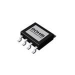
| 产品图片 |
|
| rohs | 符合RoHS无铅 / 符合限制有害物质指令(RoHS)规范要求 |
| 产品系列 | 内存,电可擦除可编程只读存储器,ROHM Semiconductor BR24L01AFJ-WE2- |
| 数据手册 | |
| 产品型号 | BR24L01AFJ-WE2 |
| 产品培训模块 | http://www.digikey.cn/PTM/IndividualPTM.page?site=cn&lang=zhs&ptm=30341 |
| 产品目录页面 | |
| 产品种类 | 电可擦除可编程只读存储器 |
| 供应商器件封装 | 8-SOP-J |
| 其它名称 | BR24L01AFJ-WE2CT |
| 包装 | 剪切带 (CT) |
| 商标 | ROHM Semiconductor |
| 存储器类型 | EEPROM |
| 存储容量 | 1 kbit |
| 安装风格 | SMD/SMT |
| 封装 | Reel |
| 封装/外壳 | 8-SOIC(0.154",3.90mm 宽) |
| 封装/箱体 | SOP-J8 |
| 工作温度 | -40°C ~ 85°C |
| 工作电流 | 2 mA |
| 工作电源电压 | 2.5 V, 3.3 V, 5 V |
| 工厂包装数量 | 2500 |
| 接口 | I²C,2 线串口 |
| 接口类型 | I2C |
| 数据保留 | 40 yr |
| 最大工作温度 | + 85 C |
| 最大工作电流 | 2 mA |
| 最大时钟频率 | 0.4 MHz |
| 最小工作温度 | - 40 C |
| 标准包装 | 1 |
| 格式-存储器 | EEPROMs - 串行 |
| 电压-电源 | 1.8 V ~ 5.5 V |
| 电源电压-最大 | 5.5 V |
| 电源电压-最小 | 1.8 V |
| 组织 | 128 x 8 |
| 速度 | 400kHz |


- 商务部:美国ITC正式对集成电路等产品启动337调查
- 曝三星4nm工艺存在良率问题 高通将骁龙8 Gen1或转产台积电
- 太阳诱电将投资9.5亿元在常州建新厂生产MLCC 预计2023年完工
- 英特尔发布欧洲新工厂建设计划 深化IDM 2.0 战略
- 台积电先进制程称霸业界 有大客户加持明年业绩稳了
- 达到5530亿美元!SIA预计今年全球半导体销售额将创下新高
- 英特尔拟将自动驾驶子公司Mobileye上市 估值或超500亿美元
- 三星加码芯片和SET,合并消费电子和移动部门,撤换高东真等 CEO
- 三星电子宣布重大人事变动 还合并消费电子和移动部门
- 海关总署:前11个月进口集成电路产品价值2.52万亿元 增长14.8%


PDF Datasheet 数据手册内容提取
Datasheet Serial EEPROM Series Standard EEPROM 2 I C BUS EEPROM (2-Wire) BR24Lxxx-W Series (1K 2K 4K 8K 16K 32K 64K) ●General Description BR24Lxxx-W series is a serial EEPROM of I2C BUS interface method ●Features ●Packages W(Typ.) x D(Typ.) x H(Max.) (cid:132) Completely conforming to the world standard I2C BUS. All controls available by 2 ports of serial clock (SCL) and serial data (SDA) (cid:132) Other devices than EEPROM can be connected to the same port, saving microcontroller port SOP8 TSSOP-B8 (cid:132) 1.8V to 5.5V *1 single power source action most 5 .00mm x 6.20mm x 1.71mm 3.00mm x 6.40mm x 1.20mm suitable for battery use (cid:132) Page write mode useful for initial value write at factory shipment (cid:132) Highly reliable connection by Au pad and Au wire (cid:132) Auto erase and auto end function at data write (cid:132) Low current consumption SOP-J8 TSSOP-B8J (cid:190) At write operation (5V) : 1.2mA (Typ.) *2 4.90mm x 6.00mm x 1.65mm 3.00mm x 4.90mm x 1.10mm (cid:190) At read operation (5V) : 0.2mA (Typ.) (cid:190) At standby operation (5V) : 0.1μA (Typ.) (cid:132) Write mistake prevention function (cid:190) Write (write protect) function added (cid:132) Write mistake prevention function at low voltage SSOP-B8 MSOP8 (cid:132) Data rewrite up to 1,000,000 times 3.00mm x 6.40mm x 1.35mm 2.90mm x 4.00mm x 0.90mm (cid:132) Data kept for 40 years (cid:132) Noise filter built in SCL / SDA terminal (cid:132) Shipment data all address FFh *1 BR24L02-W, BR24L16-W, BR24L32-W : 1.7V to 5.5V VSON008X2030 *2 BR24L32-W, BR24L64-W : 1.5mA 2.00mm x 3.00mm x 0.60mm ●Page write Number of 8Byte 16Byte 32Byte Pages BR24L04-W Product BR24L01A-W BR24L32-W BR24L08-W number BR24L02-W BR24L64-W BR24L16-W ●BR24Lxxx-W Series Bit Power source VSON008 Capacity Type SOP8 SOP-J8 SSOP-B8 TSSOP-B8 MSOP8 TSSOP-B8J format Voltage X2030 1Kbit 128×8 BR24L01A-W 1.8V to 5.5V ● ● ● ● ● ● ● 2Kbit 256×8 BR24L02-W 1.7V to 5.5V ● ● ● ● ● ● ● 4Kbit 512×8 BR24L04-W 1.8V to 5.5V ● ● ● ● ● ● ● 8Kbit 1K×8 BR24L08-W 1.8V to 5.5V ● ● ● ● ● ● ● 16Kbit 2K×8 BR24L16-W 1.7V to 5.5V ● ● ● ● ● ● 32Kbit 4K×8 BR24L32-W 1.7V to 5.5V ● ● ● ● 64Kbit 8K×8 BR24L64-W 1.8V to 5.5V ● ● ○Product structure:Silicon monolithic integrated circuit ○This product is not designed protection against radioactive rays www.rohm.com TSZ02201-0R2R0G100290-1-2 ©2012 ROHM Co., Ltd. All rights reserved. 1/36 TSZ22111・14・001 21.AUG.2012 Rev.001
BR24Lxxx-W Series (1K 2K 4K 8K 16K 32K 64K) Datasheet ●Absolute Maximum Ratings (Ta=25℃) Parameter Symbol Ratings Unit Remarks Supply Voltage V -0.3 to +6.5 V CC 450 (SOP8) When using at Ta=25℃ or higher 4.5mW to be reduced per 1℃. 450 (SOP-J8) When using at Ta=25℃ or higher 4.5mW to be reduced per 1℃. 300 (SSOP-B8) When using at Ta=25℃ or higher 3.0mW to be reduced per 1℃. Power Dissipation Pd 330 (TSSOP-B8) mW When using at Ta=25℃ or higher 3.3mW to be reduced per 1℃. 310 (TSSOP-B8J) When using at Ta=25℃ or higher 3.1mW to be reduced per 1℃. 310 (MSOP8) When using at Ta=25℃ or higher 3.1mW to be reduced per 1℃. 300 (VSON008X2030) When using at Ta=25℃ or higher 3.0mW to be reduced per 1℃. Storage Temperature Tstg -65 to +125 ℃ Operating Temperature Topr -40 to +85 ℃ Terminal Voltage ‐ -0.3 to Vcc+1.0 V ●Memory cell characteristics (Ta=25℃, Vcc=1.8V to 5.5V)*1 Limits Parameter Unit Min. Typ. Max. Number of data rewrite times *2 1,000,000 - - Times Data hold years *2 40 - - Years ○Shipment data all address FFh *1 BR24L02/16/32-W : 1.7V to 5.5V *2 Not 100% TESTED ●Recommended Operating Ratings Parameter Symbol Ratings Unit Power source voltage Vcc 1.8 to 5.5 *1 V Input voltage V 0 to Vcc IN *1 BR24L02/16/32-W : 1.7V to 5.5V ●Electrical Characteristics (Unless otherwise specified, Ta=-40℃ to +85℃, VCC=1.8V to 5.5V) *1 Limits Parameter Symbol Unit Conditions Min. Typ. Max. “HIGH” input voltage 1 VIH1 0.7Vcc - Vcc +1.0 *2 V 2.5≦Vcc≦5.5V “LOW” input voltage 1 VIL1 -0.3 *2 - 0.3 Vcc V 2.5≦Vcc≦5.5V “HIGH” input voltage 2 VIH2 0.8Vcc - Vcc +1.0 *2 V 1.8≦Vcc<2.5V “LOW” input voltage 2 VIL2 -0.3 *2 - 0.2 Vcc V 1.8≦Vcc<2.5V “HIGH” input voltage 3 *3 VIH3 0.8Vcc - Vcc +1.0 V 1.7≦Vcc<1.8V “HIGH” input voltage 3 *4 VIH3 0.9Vcc - Vcc +1.0 V 1.7≦Vcc<1.8V “LOW” input voltage 3 *2 VIL3 -0.3 - 0.1 Vcc V 1.7≦Vcc<1.8V “LOW” output voltage 1 VOL1 - - 0.4 V IOL=3.0mA, 2.5V≦Vcc≦5.5V, (SDA) “LOW” output voltage 2 VOL2 - - 0.2 V IOL=0.7mA, 1.7V≦Vcc<2.5V, (SDA) Input leak current ILI -1 - 1 μA VIN=0V to Vcc Output leak current ILO -1 - 1 μA VOUT=0V to Vcc, (SDA) 2.0 *5 Vcc=5.5V,fSCL=400kHz, tWR=5ms, ICC1 - - mA Current consumption at 3.0 *6 Byte write, Page write action Vcc=5.5V,fSCL=400kHz ICC2 - - 0.5 mA Random read, current read,sequential read Vcc=5.5V, SDA・SCL=Vcc Standby current ISB - - 2.0 μA A0, A1, A2=GND, WP=GND *1 BR24L02/16/32-W : 1.7V to 5.5V, *2 BR24L16/32-W, *3 BR24L02/16-W, *4 BR24L32-W *5 BR24L01A/02/04/08/16-W, *6 BR24L32/64-W www.rohm.com TSZ02201-0R2R0G1000290-1-2 ©2012 ROHM Co., Ltd. All rights reserved. 2/36 TSZ22111・15・001 21.AUG.2012 Rev.001
BR24Lxxx-W Series (1K 2K 4K 8K 16K 32K 64K) Datasheet ●Action timing characteristics (Unless otherwise specified, Ta=-40℃ to +85℃, VCC=1.8V to 5.5V)*1 FAST-MODE STANDARD-MODE Parameter Symbol 2.5V≦Vcc≦5.5V 1.8V≦Vcc≦5.5V Unit Min. Typ. Max. Min. Typ. Max. SCL frequency fSCL - - 400 - - 100 kHz Data clock “HIGH“ time tHIGH 0.6 - - 4.0 - - μs Data clock “LOW“ time tLOW 1.2 - - 4.7 - - μs SDA, SCL rise time *2 tR - - 0.3 - - 1.0 μs SDA, SCL fall time *2 tF - - 0.3 - - 0.3 μs Start condition hold time tHD:STA 0.6 - - 4.0 - - μs Start condition setup time tSU:STA 0.6 - - 4.7 - - μs Input data hold time tHD:DAT 0 - - 0 - - ns Input data setup time tSU:DAT 100 - - 250 - - ns Output data delay time tPD 0.1 - 0.9 0.2 - 3.5 μs Output data hold time tDH 0.1 - - 0.2 - - μs Stop condition setup time tSU:STO 0.6 - - 4.7 - - μs Bus release time before transfer start tBUF 1.2 - - 4.7 - - μs Internal write cycle time tWR - - 5 - - 5 ms Noise removal valid period (SDA, SCL terminal) tI - - 0.1 - - 0.1 μs WP hold time tHD:WP 0 - - 0 - - ns WP setup time tSU:WP 0.1 - - 0.1 - - μs WP valid time tHIGH:WP 1.0 - -- 1.0 - - μs *1 BR24L02/16/32-W : 1.7V to 5.5V *2 Not 100% tested ●FAST-MODE and STANDARD-MODE FAST-MODE and STANDARD-MODE are of same actions, and mode is changed. They are distinguished by action speeds. 100kHz action is called STANDARD-MODE, and 400kHz action is called FAST-MODE. This action frequency is the maximum action frequency, so 100kHz clock may be used in FAST-MODE. When power source voltage goes down, action at high speed is not carried out, therefore, at Vcc=2.5V to 5.5V , 400kHz, namely, action is made in FASTMODE. (Action is made also in STANDARD-MODE) Vcc=1.8V to 2.5V is only action in 100kHz STANDARD-MODE. www.rohm.com TSZ02201-0R2R0G1000290-1-2 ©2012 ROHM Co., Ltd. All rights reserved. 3/36 TSZ22111・15・001 21.AUG.2012 Rev.001
BR24Lxxx-W Series (1K 2K 4K 8K 16K 32K 64K) Datasheet ●Sync data input / output timing tR tF tHIGH SCL SCL tHD:STA tSU:DAT tLOW tHD:DAT tSU:STA tHD:STA tSU:STO SDA ((in入pu力t) ) SDA tBUF tPD tDH SDA START BIT STOP BIT (o(u出tp力ut)) ○Input read at the rise edge of SCL ○Data output in sync with the fall of SCL Figure 1-(a) Sync data input / output timing Figure 1-(b) Start-stop bit timing SCL SCL DATA(1) DATA(n) SDA D1 D0 ACK ACK SDA D0 ACK tWR Write data tWR WP スSトtッopプ cコoンndデitiィoシnョン (n-th address) Stop condition Start condition tSU:WP tHD:WP Figure 1-(c) Write cycle timing Figure 1-(d) WP timing at write execution SCL DATA(1) DATA(n) SDA D1 D0 ACK ACK tHIGH:WP tWR WP ○At write execution, in the area from the D0 taken clock rise of the first DATA(1), to tWR, set WP=“LOW”. ○By setting WP “HIGH” in the area, write can be cancelled. When it is set WP=“HIGH” during tWR, write is forcibly ended, and data of address under access is not guaranteed, therefore write it once again. Figure 1-(e) WP timing at write cancel www.rohm.com TSZ02201-0R2R0G1000290-1-2 ©2012 ROHM Co., Ltd. All rights reserved. 4/36 TSZ22111・15・001 21.AUG.2012 Rev.001
BR24Lxxx-W Series (1K 2K 4K 8K 16K 32K 64K) Datasheet ●Block Diagram *2 A0 1 1Kbit to 64Kbit EEPROM array 8 Vcc *1 7bit 11bit 8bit 12bit 8bit 9bit 13bit 10bit *2 A1 2 Address 78bbiitt 1112bbiitt Slave - word Data 7 WP decoder *1 9bit 13bit address register register 10bit START STOP *2 A2 3 6 SCL Control circuit ACK High voltage Power source GND 4 generating circuit voltage detection 5 SDA *1 7bit : BR24L01A-W 10bit : BR24L08-W *2 A0=N.C. : BR24L04-W 8bit : BR24L02-W 11bit : BR24L16-W A0, A1=N.C. : BR24L08-W 9bit : BR24L04-W 12bit : BR24L32-W A0, A1= N.C. A2=Don’t Use : BR24L16-W 13bit : BR24L64-W ●Pin Configuration (TOP VIEW) A0 11 81 Vcc BR24L01A-W A1 21 BBRR2244LL0024--WW 71 WP BR24L08-W A2 31 BR24L16-W 61 SCL BR24L32-W GND 4 BR24L64-W 5 SDA 1 1 ●Pin Descriptions Terminal Input / Function name output BR24L01A-W BR24L02-W BR24L04-W BR24L08-W BR24L16-W BR24L32-W BR24L64-W A0 Input Slave address setting Not connected Slave address setting A1 Input Slave address setting Not connected Slave address setting A2 Input Slave address setting Not used Slave address setting GND - Reference voltage of all input / output, 0V Input / SDA Slave and word address, Serial data input serial data output output SCL Input Serial clock input WP Input Write protect terminal Vcc - Connect the power source. www.rohm.com TSZ02201-0R2R0G1000290-1-2 ©2012 ROHM Co., Ltd. All rights reserved. 5/36 TSZ22111・15・001 21.AUG.2012 Rev.001
BR24Lxxx-W Series (1K 2K 4K 8K 16K 32K 64K) Datasheet ●Typical Performance Curves (The following values are Typ. ones.) Figure 3. "L" Input VoltageVIL1,2 Figure 2. "H" Input Voltage VIH1,2 (SCL, SDA, WP) Figure 4. "L" Output Voltage1 VOL1-IOL1 Figure 5."L" Output Voltage VOL2-IOL2 (Vcc=2.5V) (Vcc=1.8V) www.rohm.com TSZ02201-0R2R0G1000290-1-2 ©2012 ROHM Co., Ltd. All rights reserved. 6/36 TSZ22111・15・001 21.AUG.2012 Rev.001
BR24Lxxx-W Series (1K 2K 4K 8K 16K 32K 64K) Datasheet ●Typical Performance Curves‐Continued Figure 6. Input Leak Current ILI Figure 7.Output Leak Current ILO (SDA) (SCL, WP) A] m 1[ C C I Figure 8. Current consumption at WRITE action ICC1 Figure 9.Current consumption at WRITE actionICC1 (fscl=400kHz) (fscl=400kHz) www.rohm.com TSZ02201-0R2R0G1000290-1-2 ©2012 ROHM Co., Ltd. All rights reserved. 7/36 TSZ22111・15・001 21.AUG.2012 Rev.001
BR24Lxxx-W Series (1K 2K 4K 8K 16K 32K 64K) Datasheet ●Typical Performance Curves‐Continued 1PIN MARK LOT Number LOT Number Figure 10. Current consumption at READ action ICC2 Figure 11.Current consumption at WRITEaction ICC1 (fscl=400kHz) (fscl=100kHz) 1PIN MARK Figure 12. Current consumption at WRITE action ICC1 Figure 13.Current consumption at READaction ICC2 (fscl=100kHz) (fscl=100kHz) www.rohm.com TSZ02201-0R2R0G1000290-1-2 ©2012 ROHM Co., Ltd. All rights reserved. 8/36 TSZ22111・15・001 21.AUG.2012 Rev.001
BR24Lxxx-W Series (1K 2K 4K 8K 16K 32K 64K) Datasheet ●Typical Performance Curves‐Continued Figure 14. Standby current ISB Figure 15. SCL frequency fSCL Figure 16. Data clock “H” time tHIGH Figure 17.Data clock “L” time tLOW www.rohm.com TSZ02201-0R2R0G1000290-1-2 ©2012 ROHM Co., Ltd. All rights reserved. 9/36 TSZ22111・15・001 21.AUG.2012 Rev.001
BR24Lxxx-W Series (1K 2K 4K 8K 16K 32K 64K) Datasheet ●Typical Performance Curves‐Continued Figure 18. Start condition hold time tHD:STA Figure 19.Start condition setup time tHD:STA Figure 20. Input data hold time tHD :DAT(HIGH) Figure 21.Input data hold time tHD:DAT(LOW) www.rohm.com TSZ02201-0R2R0G1000290-1-2 ©2012 ROHM Co., Ltd. All rights reserved. 10/36 TSZ22111・15・001 21.AUG.2012 Rev.001
BR24Lxxx-W Series (1K 2K 4K 8K 16K 32K 64K) Datasheet ●Typical Performance Curves‐Continued Figure 22. Input data setup time tSU:DAT(HIGH) Figure 23.Input data setup time tSU:DAT(LOW) Figure 25.Output data delay time tPD1 Figure 24. Output data delay time tPD0 www.rohm.com TSZ02201-0R2R0G1000290-1-2 ©2012 ROHM Co., Ltd. All rights reserved. 11/36 TSZ22111・15・001 21.AUG.2012 Rev.001
BR24Lxxx-W Series (1K 2K 4K 8K 16K 32K 64K) Datasheet ●Typical Performance Curves‐Continued Figure 26. Bus release time before transfer start tBUF Figure 27.Internal write cycle time tWR Figure 28. Noise removal valid time tl(SCLH) Figure 29.Noise removal valid time tl(SCLL) www.rohm.com TSZ02201-0R2R0G1000290-1-2 ©2012 ROHM Co., Ltd. All rights reserved. 12/36 TSZ22111・15・001 21.AUG.2012 Rev.001
BR24Lxxx-W Series (1K 2K 4K 8K 16K 32K 64K) Datasheet ●Typical Performance Curves‐Continued Figure 30. Noise removal valid time tl (SDAH) Figure 31.Noise removal valid time tl (SDAL) Figure 32. WP setup time tSU:WP Figure 33. WP valid time tHIGH:WP www.rohm.com TSZ02201-0R2R0G1000290-1-2 ©2012 ROHM Co., Ltd. All rights reserved. 13/36 TSZ22111・15・001 21.AUG.2012 Rev.001
BR24Lxxx-W Series (1K 2K 4K 8K 16K 32K 64K) Datasheet ●I2C BUS Communication ○I2C BUS data communication I2C BUS data communication starts by start condition input, and ends by stop condition input. Data is always 8bit long, and acknowledge is always required after each byte. I2C BUS carries out data transmission with plural devices connected by 2 communication lines of serial data (SDA) and serial clock (SCL). Among devices, there are “master” that generates clock and control communication start and end, and “slave” that is controlled by address peculiar to devices. EEPROM becomes “slave”. And the device that outputs data to bus during data communication is called “transmitter”, and the device that receives data is called “receiver”. SDA SCL 1-7 8 9 1-7 8 9 1-7 8 9 S P START ADDRESS R/W ACK DATA ACK DATA ACK STOP condition condition Figure 34. Data transfer timing ○Start condition (Start bit recognition) ・Before executing each command, start condition (start bit) where SDA goes from 'HIGH' down to 'LOW' when SCL is 'HIGH' is necessary. ・This IC always detects whether SDA and SCL are in start condition (start bit) or not, therefore, unless this confdition is satisfied, any command is executed. ○Stop condition (stop bit recongnition) ・Each command can be ended by SDA rising from 'LOW' to 'HIGH' when stop condition (stop bit), namely, SCL is 'HIGH' ○Acknowledge (ACK) signal ・This acknowledge (ACK) signal is a software rule to show whether data transfer has been made normally or not. In master and slave, the device (μ-COM at slave address input of write command, read command, and this IC at data output of read command) at the transmitter (sending) side releases the bus after output of 8bit data. ・The device (this IC at slave address input of write command, read command, and μ-COM at data output of read command) at the receiver (receiving) side sets SDA 'LOW' during 9 clock cycles, and outputs acknowledge signal (ACK signal) showing that it has received the 8bit data. ・This IC, after recognizing start condition and slave address (8bit), outputs acknowledge signal (ACK signal) 'LOW'. ・Each write action outputs acknowledge signal (ACK signal) 'LOW', at receiving 8bit data (word address and write data). ・Each read action outputs 8bit data (read data), and detects acknowledge signal (ACK signal) 'LOW'. ・When acknowledge signal (ACK signal) is detected, and stop condition is not sent from the master (μ-COM) side, this IC continues data output. When acknowledge signal (ACK signal) is not detected, this IC stops data transfer, and recognizes stop cindition (stop bit), and ends read action. And this IC gets in status. www.rohm.com TSZ02201-0R2R0G1000290-1-2 ©2012 ROHM Co., Ltd. All rights reserved. 14/36 TSZ22111・15・001 21.AUG.2012 Rev.001
BR24Lxxx-W Series (1K 2K 4K 8K 16K 32K 64K) Datasheet ○Device addressing ・Output slave address after start condition from master. ・The significant 4 bits of slave address are used for recognizing a device type. The device code of this IC is fixed to '1010'. ・Next slave addresses (A2 A1 A0 --- device address) are for selecting devices, and plural ones can be used on a same bus according to the number of device addresses. ・The most insignificant bit (R/W --- READ / WRITE) of slave address is used for designating write or read action, and is as shown below. Setting R / W to 0 ------- write (setting 0 to word address setting of random read) Setting R / W to 1 ------- read Maximum number of Type Slave address connected buses BR24L01A-W 1 0 1 0 A2 A1 A0 R/W― 8 BR24L02-W 1 0 1 0 A2 A1 A0 R/W― 8 BR24L04-W 1 0 1 0 A2 A1 PS R/W― 4 BR24L08-W 1 0 1 0 A2 P1 P0 R/W― 2 BR24L16-W 1 0 1 0 P2 P1 P0 R/W― 1 BR24L32-W 1 0 1 0 A2 A1 A0 R/W― 8 BR24L64-W 1 0 1 0 A2 A1 A0 R/W― 8 PS, P0 to P2 are page select bits. Note) Up to 4 units BR24L04-W, up to 2 units of BR24L08-W, and one unit of BR24L16-W can be connected. Device address is set by 'H' and 'L' of each pin of A0, A1, and A2. www.rohm.com TSZ02201-0R2R0G1000290-1-2 ©2012 ROHM Co., Ltd. All rights reserved. 15/36 TSZ22111・15・001 21.AUG.2012 Rev.001
BR24Lxxx-W Series (1K 2K 4K 8K 16K 32K 64K) Datasheet ●Write Command ○Write cycle ・Arbitrary data is written to EEPROM. When to write only 1 byte, byte write is normally used, and when to write continuous data of 2 bytes or more, simultaneous write is possible by page write cycle. The maximum number of write bytes is specified per device of each capacity. Up to 32 arbitrary bytes can be written. (In the case of BR24L32 / L64-W) S W T R S A I T R SLAVE T WORD DATA O T ADDRESS E ADDRESS P SDA *1 As for WA7, BR24L01A-W becomes Don’t care. LIN E 1 0 1 0 A2 A1 A0 W7A W0A D7 D0 R A *1 A A Note) / C C C W K K K Figure 35. Byte write cycle (BR24L01A/02/04/08/16-W) S W T R S A I T R SLAVE T 1st WORD 2nd WORD DATA O T ADDRESS E ADDRESS ADDRESS P SLIDN AE 1 0 1 0 A2 A1 A0 * * * W12AW 11A W0A D7 D0 *1 As for WA12, BR24L32-W becomes Don’t care. R A A A A Note) / C *1 C C C W K K K K Figure 36. Byte write cycle (BR24L32/64-W) ST WR S A I T R SLAVE T WORD *2 O T ADDRESS E ADDRESS(n) DATA(n) DATA(n+15) P *1 As for WA7, BR24L01A-W becomes Don’t care. SD A LIN E 1 0 1 0 A2A 1A 0 W7A W0A D7 D0 D0 *2 As for BR24L01A/02-W becomes (n+7). R A A A A Note) / C *1 C C C W K K K K Figure 37. Page write cycle (BR24L01A/02/04/08/16-W) ST WR S RAT ADSDLARVEES S ETI A1DsDt RWEOSRSD(n ) A2DnDdR WEOSRS(Dn ) DATA(n) DATA(n+31) OPT SDA *1 As for WA12, BR24L32-W becomes Don’t care. LIN E 1 0 1 0 A2A 1A 0 * * * W12A W11A W0A D7 D0 D0 Note) WR/ CAK *1 CAK CAK CAK CAK Figure 38. Page write cycle (BR24L32/64-W) ・Data is written to the address designated by word address (n-th address) ・By issuing stop bit after 8bit data input, write to memory cell inside starts. ・When internal write is started, command is not accepted for tWR (5ms at maximum). ・By page write cycle, the following can be written in bulk : Up to 8 bytes ( BR24L01A-W, BR24L02-W) : Up to 16bytes (BR24L04-W, BR24L08-W,BR24L16-W) : Up to 32bytes (BR24L32-W, BR24L64-W) And when data of the maximum bytes or higher is sent, data from the first byte is overwritten. (Refer to "Internal address increment" in Page 17.) ・As for page write cycle of BR24L01A-W and BR24L02-W, after the significant 5 bits (4 significant bits in BR24L01-W) of word address are designated arbitrarily, and as for page write command of BR24L04-W, BR24L08-W, and BR24L16-W, after page select bit (PS) of slave address is designated arbitrarily, by continuing data input of 2 bytes or more, the address of insignificant 4 bits (insignificant 3 bit in BR24L01A-W, and BR24L02-W) is incremented internally, and data up to 16 bytes (up to 8 bytes in BR24L01A-W and BR24L02-W) can be written. ・As for page write cycle of BR24L32-W and BR24L64-W, after the significant 7 bits (in the case of BR24L32-W) of word address, or the significant 8 bits (in the case of BR24L64-W) of word address are designated arbitrarily, by continuing data input of 2 byte or more, the address of insignificant 5 bits is incremented internally, and data up to 32 bytes can be written. Note) *1 In BR24L16-W, A2 becomes P2. *1 *2 *3 *2 In BR24L08-W, BR24L16-W, A1 becomes P1. 1 0 1 0 A2A 1A0 *3 In BR24L04-W, A0 becomes PS, and in BR24L08-W and BR24L16-W, A0 becomes P0. Figure 39. Difference of slave address of each type www.rohm.com TSZ02201-0R2R0G1000290-1-2 ©2012 ROHM Co., Ltd. All rights reserved. 16/36 TSZ22111・15・001 21.AUG.2012 Rev.001
BR24Lxxx-W Series (1K 2K 4K 8K 16K 32K 64K) Datasheet ○Notes on write cycle continuous input At STOP (stop bit), write starts. S W S T R S T ART ADSLDARVEES S TEI ADDWROERSDS( n) DATA(n) DATA(n+7)**23 OPT ART SDA *1 LINE 1 0 1 0 A2 A1A 0 W7A W0A D7 D0 D0 1 0 10 R A A A A Note) / C C C C Next command W K K K K tWR(maximum : 5ms) Command is not accepted for this period. *1 BR24L01A-W becomes Don’t care. *2 BR24L04-W, BR24L08-W, and BR24L16-W become (n+15). *3 BR24L32-W and BR24L64-W become (n+31). Figure 40. Page write cycle Note) *1 *2 *3 1 0 1 0 A2A 1A 0 *1 In BR24L16-W, A2 becomes P2. *2 In BR24L08-W, BR24L16-W, A1 becomes P1. *3 In BR24L04-W, A0 becomes PS, and in BR24L08-W and in BR24L16-W, A0 becomes P0. Figure 41. Difference of each type of slave address ○Notes on page write cycle List of numbers of page write Number of Pages 8Byte 16Byte 32Byte BR24L04-W Product BR24L01A-W BR24L32-W BR24L08-W number BR24L02-W BR24L64-W BR24L16-W The above numbers are maximum bytes for respective types. Any bytes below these can be written. In the case BR24L02-W, 1 page=8bytes, but the page write cycle write time is 5ms at maximum for 8byte bulk write. It does not stand 5ms at maximum × 8byte=40ms(Max.). www.rohm.com TSZ02201-0R2R0G1000290-1-2 ©2012 ROHM Co., Ltd. All rights reserved. 17/36 TSZ22111・15・001 21.AUG.2012 Rev.001
BR24Lxxx-W Series (1K 2K 4K 8K 16K 32K 64K) Datasheet ○Internal address increment Page write mode (in the case of BR24L02-W) WA7 ----- WA4 WA3 WA2 WA1 WA0 0 ----- 0 0 0 0 0 Increment 0 ----- 0 0 0 0 1 0 ----- 0 0 0 1 0 --------- --------- --------- 0 ----- 0 0 1 1 0 06h 0 ----- 0 0 1 1 1 0 ----- 0 0 0 0 0 Significant bit is fixed. No digit up For example, when it is started from address 06h,therefore, increment is made as below, 06h → 07h → 00h → 01h ---, which please note. * 06h・・・06 in hexadecimal, therefore, 00000110 becomes a binary number. ○Write protect (WP) terminal ・Write protect (WP) function When WP terminal is set Vcc (H level), data rewrite of all addresses is prohibited. When it is set GND (L level), data rewrite of all address is enabled. Be sure to connect this terminal to Vcc or GND, or control it to H level or L level. Do not use it open. At extremely low voltage at power ON / OFF, by setting the WP terminal 'H', mistake write can be prevented. During tWR, set the WP terminal always to 'L'. If it is set 'H', write is forcibly terminated. www.rohm.com TSZ02201-0R2R0G1000290-1-2 ©2012 ROHM Co., Ltd. All rights reserved. 18/36 TSZ22111・15・001 21.AUG.2012 Rev.001
BR24Lxxx-W Series (1K 2K 4K 8K 16K 32K 64K) Datasheet ●Read Command ○Read cycle Data of EEPROM is read. In read cycle, there are random read cycle and current read cycle. Random read cycle is a command to read data by designating address, and is used generally. Current read cycle is a command to read data of internal address register without designating address, and is used when to verify just after write cycle. In both the read cycles, sequential read cycle is available, and the next address data can be read in succession. S W S It is necessary to input 'H' to AT RI AT RE ST the last ACK. RT ADSDLARVEES S ET ADDWROERSDS (n) RT ADSDLARVEESS DA DATA(n) OP SDA LINE 1 0 1 0 A2A 1A 0 W7A W0A 1 0 1 0 A2A1A0 D7 D0 Note) WR/ CAK *1 CKA WR/ CKA CKA *1 As for WA7, BR24L01A-W become Don’t care. Figure 42. Random read cycle (BR24L01A/02/04/08/16-W) ST WR ST R S ART ADSDLARVEES S TEI AD1DstR WESOSR(Dn) AD2nDdR WESOSR(Dn ) ART ADSLDARVEESS DAE DATA(n) OPT SDA LINE 1 0 10 A2 A1A 0 * **W12A W11A W0A 10 10A2 A1A0 D7 D0 R A A A R A A Note) / C *1 C C / C C *1 As for WA12, BR24L32-W become Don’t care. W K K K W K K Figure 43. Random read cycle (BR24L32/64 -W) SAT RE ST It is necessary to input 'H' to R SLAVE A O the last ACK. T ADDRESS D DATA(n) P SDA LINE 1 0 1 0 A2A 1A 0 D7 D0 R A A Note) / C C W K K Figure 44. Current read cycle ST R S ART ADSDLARVEES S DAE DATA(n) DATA(n+x) OPT SLIDNAE 1 0 1 0 A2 A1A 0 D7 D0 D7 D0 R A A A A Note) W/ CK CK CK CK Figure 45. Sequential read cycle (in the case of current read cycle) ・In random read cycle, data of designated word address can be read. ・When the command just before current read cycle is random read cycle, current read cycle (each including sequential read cycle), data of incremented last read address (n)-th address, i.e., data of the (n+1)-th address is output. ・When ACK signal 'LOW' after D0 is detected, and stop condition is not sent from master (μ-COM) side, the next address data can be read in succession. ・Read cycle is ended by stop condition where 'H' is input to ACK signal after D0 and SDA signal is started at SCL signal 'H' . ・When 'H' is not input to ACK signal after D0, sequential read gets in, and the next data is output. Therefore, read command cycle cannot be ended. When to end read command cycle, be sure input stop condition to input 'H' to ACK signal after D0, and to start SDA at SCL signal 'H'. ・Sequential read is ended by stop condition where 'H' is input to ACK signal after arbitrary D0 and SDA is started at SCL signal 'H'. Note) *1 *2 *3 *1 In BR24L16-W, A2 becomes P2. 1 0 1 0 A2A 1A 0 *2 In BR24L08-W, BR24L16-W, A1 becomes P1. *3 In BR24L04-W, A0 becomes PS, and in BR24L08-W and BR24L16-W, A0 becomes P0. Figure 46. Difference of slave address of each type www.rohm.com TSZ02201-0R2R0G1000290-1-2 ©2012 ROHM Co., Ltd. All rights reserved. 19/36 TSZ22111・15・001 21.AUG.2012 Rev.001
BR24Lxxx-W Series (1K 2K 4K 8K 16K 32K 64K) Datasheet ●Software reset Software reset is executed when to avoid malfunction after power on, and to reset during command input. Software reset has several kinds, and 3 kinds of them are shown in the figure below. (Refer to Figure 47(a), Figure 47(b), and Figure47(c).) In dummy clock input area, release the SDA bus ('H' by pull up). In dummy clock area, ACK output and read data '0' (both 'L' level) may be output from EEPROM, therefore, if 'H' is input forcibly, output may conflict and over current may flow, leading to instantaneous power failure of system power source or influence upon devices. Dummy clock×14 Start×2 SCL 1 2 13 14 Normal command SDA Normal command Figure 47-(a) The case of dummy clock +START+START+ command input Start Dummy clock×9 Start SCL 1 2 8 9 Normal command SDA Normal command Figure 47-(b) The case of START +9 dummy clocks +START+ command input Start×9 SCL 1 2 3 7 8 9 Normal command SDA Normal command * Start command from START input. Figure 47-(c) START×9+ command input ●Acknowledge polling During internal write execution, all input commands are ignored, therefore ACK is not sent back. During internal automatic write execution after write cycle input, next command (slave address) is sent, and if the first ACK signal sends back 'L', then it means end of write action, while if it sends back 'H', it means now in writing. By use of acknowledge polling, next command can be executed without waiting for tWR = 5ms. When to write continuously, R/W = 0, when to carry out current read cycle after write, slave address R/W = 1 is sent, and if ACK signal sends back 'L', then execute word address input and data output and so forth. During internal write, First write command ACK = HIGH is sent back. START Write command STOP START Sadladvree ss ACKH t START Sadladvree ss ACKH WR Second write command S A S A A A S … TAR Sadladvree ss CKH TAR Sadladvree ss CKL Wadodrrde ss CKL Data CKL TOP T T tWR After completion of internal write, ACK=LOW is sent back, so input next word address and data in succession. Figure 48. Case to continuously write by acknowledge polling www.rohm.com TSZ02201-0R2R0G1000290-1-2 ©2012 ROHM Co., Ltd. All rights reserved. 20/36 TSZ22111・15・001 21.AUG.2012 Rev.001
BR24Lxxx-W Series (1K 2K 4K 8K 16K 32K 64K) Datasheet ●WP valid timing (write cancel) WP is usually fixed to 'H' or 'L', but when WP is used to cancel write cycle and so forth, pay attention to the following WP valid timing. During write cycle execution, in cancel valid area, by setting WP='H', write cycle can be cancelled. In both byte write cycle and page write cycle, the area from the first start condition of command to the rise of clock to taken in D0 of data(in page write cycle, the first byte data) is cancel invalid area. WP input in this area becomes Don't care. Set the setup time to rise of D0 taken SCL 100ns or more. The area from the rise of SCL to take in D0 to the end of internal automatic write (tWR) is cancel valid area. And, when it is set WP='H' during tWR, write is ended forcibly, data of address under access is not guaranteed, therefore, write it once again. (Refer to Figure 49.) After execution of forced end by WP, standby status gets in, so there is no need to wait for tWR (5ms at maximum). ・Rise of D0 taken clock SCL SCL ・Rise of SDA SDA D1 D0 ACK SDA D0 ACK Enlarged view Enlarged view S A A A A S SDA TAR Sadladvree ss CKL Wadodrrde ss CKL D7 D6 D5D4 D3D2D1 D0 CKL Data CKL OPT tWR T WP cancel invalid area WP cancel valid area Write forced end WP Data is not written. Data not guaranteed Figure 49. WP valid timing ●Command cancel by start condition and stop condition During command input, by continuously inputting start condition and stop condition, command can be cancelled. (Refer to Figure 50.) However, in ACK output area and during data read, SDA bus may output 'L', and in this case, start condition and stop condition cannot be input, so reset is not available. Therefore, execute software reset. And when command is cancelled by start, stop condition, during random read cycle, sequential read cycle, or current read cycle, internal setting address is not determined, therefore, it is not possible to carry out current read cycle in succession. When to carry out read cycle in succession, carry out random read cycle. SCL SDA 1 0 1 0 Start condition Stop condition Figure 50. Case of cancel by start, stop condition during slave address input www.rohm.com TSZ02201-0R2R0G1000290-1-2 ©2012 ROHM Co., Ltd. All rights reserved. 21/36 TSZ22111・15・001 21.AUG.2012 Rev.001
BR24Lxxx-W Series (1K 2K 4K 8K 16K 32K 64K) Datasheet ●I/O peripheral circuit ○Pull up resistance of SDA terminal SDA is NMOS open drain, so requires pull up resistance. As for this resistance value (R ), select an appropriate value to PU this resistance value from microcontroller V , I ,and V -I characteristics of this IC. If R is large, action frequency is IL L OL OL PU limited. The smaller the R , the larger the consumption current at action. PU ○Maximum value of R PU The maximum value of RPU is determined by the following factors. (1)SDA rise time to be determined by the capacitance (CBUS) of bus line of R and SDA should be tR or below. PU And AC timing should be satisfied even when SDA rise time is late. ○ (2)The bus electric potential A to be determined by input leak total (IL) of device connected to bus at output of 'H' to SDA bus and R should sufficiently secure the input 'H' level (V ) of microcontroller and EEPROM including PU IH recommended noise margin 0.2Vcc. Microcontroller BR24LXX VCC - ILRPU - 0.2Vcc ≧ VIH ∴ RPU 0.8VIcLc -VIH RPU SDA terminal A Ex. ) When VCC =3V, IL=10μA, VIH=0.7 VCC, from (2) IL IL 0.8×3-0.7×3 RPU ≦ 10×10-6 Bus line capacity CBUS ≦ 300 [kΩ] Figure 51. I/O circuit ○Minimum value of R PU The minimum value of R is determined by the following factors. PU (1)When IC outputs LOW, it should be satisfied that V =0.4V and I =3mA. OLMAX OLMAX VCRCP-UV OL ≦ IOL ∴ RPU ≦ VCICO-LV OL (2)VOLMAX=0.4V should secure the input 'L' level (VIL) of microcontroller and EEPROM including recommended noise margin 0.1Vcc. VOLMAX ≦ VIL-0.1 VCC Ex. ) When VCC =3V, VOL=0.4V, IOL=3mA, microcontroller, EEPROM VIL=0.3VCC from (1) 3-0.4 RPU ≧ 3×10 -3 ≧ 867 [Ω] And VOL = 0.4 [V] VIL = 0.3×3 = 0.9 [V] Therefore, the condition (2) is satisfied. ○Pull up resistance of SCL terminal When SCL control is made at CMOS output port, there is no need, but in the case there is timing where SCL becomes 'Hi-Z', add a pull up resistance. As for the pull up resistance, one of several kΩ to several ten kΩ is recommended in consideration of drive performance of output port of microcontroller. ●A0, A1, A2, WP process ○Process of device address terminals (A0,A1,A2) Check whether the set device address coincides with device address input sent from the master side or not, and select one among plural devices connected to a same bus. Connect this terminal to pull up or pull down, or Vcc or GND. And, pins (N, C, PIN) not used as device address may be set to any of 'H' , 'L', and 'Hi-Z'. Types with N.C.PIN BR24L16/F/FJ/FV/FVT/FVM/FVJ-W A0, A1, A2 BR24L08/F/FJ/FV/FVT/FVM/FVJ/NUX-W A0, A1 BR24L04/F/FJ/FV/FVT/FVM/FVJ/NUX-W A0 ○Process of WP terminal WP terminal is the terminal that prohibits and permits write in hardware manner. In 'H' status, only READ is available and WRITE of all address is prohibited. In the case of 'L', both are available. In the case of use it as an ROM, it is recommended to connect it to pull up or Vcc. In the case to use both READ and WRITE, control WP terminal or connect it to pull down or GND. www.rohm.com TSZ02201-0R2R0G1000290-1-2 ©2012 ROHM Co., Ltd. All rights reserved. 22/36 TSZ22111・15・001 21.AUG.2012 Rev.001
BR24Lxxx-W Series (1K 2K 4K 8K 16K 32K 64K) Datasheet ●Cautions on microcontroller connection ○Rs In I2C BUS, it is recommended that SDA port is of open drain input/output. However, when to use CMOS input / output of tri state to SDA port, insert a series resistance Rs between the pull up resistance Rpu and the SDA terminal of EEPROM. This is controls over current that occurs when PMOS of the microcontroller and NMOS of EEPROM are turned ON simultaneously. Rs also plays the role of protection of SDA terminal against surge. Therefore, even when SDA port is open drain input/output, Rs can be used. ACK SCL RPU RS SDA 'H' output of microcontroller 'L' output of EEPROM Microcontroller EEPROM Over current flows to SDA line by 'H' output of microcontroller and 'L' output of EEPROM. Figure 52. I/O circuit diagram Figure 53. Input / output collision timing ○Maximum value of Rs The maximum value of Rs is determined by the following relations. (1)SDA rise time to be determined by the capacity (CBUS) of bus line of Rpu and SDA should be tR or below. And AC timing should be satisfied even when SDA rise time is late. ○ (2)The bus electric potential A to be determined by Rpu and Rs the moment when EEPROM outputs 'L' to SDA bus should sufficiently secure the input 'L' level (V ) of microcontroller including recommended noise margin 0.1Vcc. IL VCC (VCC-VOL)×RS RPU A RPU+RS + VOL+0.1VCC≦VIL RS VOL VIL-VOL-0.1VCC ∴ RS ≦ × RPU IOL 1.1V CC-VIL Bus line Example) When VCC=3V, VIL=0.3VCC, VOL=0.4V, RPU=20kΩ capacity CBUS 0.3×3-0.4-0.1×3 from(2), RS ≦ × 20×103 VIL Microcontroller EEPROM 1.1× 3-0.3×3 ≦ 1.67[kΩ] Figure 54. I/O circuit ○Minimum value of Rs The minimum value of Rs is determined by over current at bus collision. When over current flows, noises in power source line, and instantaneous power failure of power source may occur. When allowable over current is defined as I, the following relation must be satisfied. Determine the allowable current in consideration of impedance of power source line in set and so forth. Set the over current to EEPROM 10mA or below. VCC ≦ I RP U RS 'L' output RS VCC ∴ RS ≧ I Over currentⅠ Example)When VCC=3V, I=10mA 'H' output 3 RS ≧ 10×10-3 Microcontroller EEPROM ≧ 300[Ω] Figure 55. I/O circuit diagram www.rohm.com TSZ02201-0R2R0G1000290-1-2 ©2012 ROHM Co., Ltd. All rights reserved. 23/36 TSZ22111・15・001 21.AUG.2012 Rev.001
BR24Lxxx-W Series (1K 2K 4K 8K 16K 32K 64K) Datasheet ●I2C BUS input / output circuit ○Input (A0,A2,SCL) Figure 56. Input pin circuit diagram ○Input / output (SDA) Figure 57. Input / output pin circuit diagram ○Input (A1, WP) Figure 58. Input pin circuit diagram ●Notes on power ON At power on, in IC internal circuit and set, Vcc rises through unstable low voltage area, and IC inside is not completely reset, and malfunction may occur. To prevent this, functions of POR circuit and LVCC circuit are equipped. To assure the action, observe the following conditions at power on. 1. Set SDA = 'H' and SCL ='L' or 'H' 2. Start power source so as to satisfy the recommended conditions of t , t , and Vbot for operating POR circuit. R OFF tR VCC Recommended conditions of tR, tOFF,Vbot tR tOFF Vbot 10ms or below 10ms or longer 0.3V or below tOFF Vbot 100ms or below 10ms or longer 0.2V or below 0 Figure 59. Rise waveform diagram www.rohm.com TSZ02201-0R2R0G1000290-1-2 ©2012 ROHM Co., Ltd. All rights reserved. 24/36 TSZ22111・15・001 21.AUG.2012 Rev.001
BR24Lxxx-W Series (1K 2K 4K 8K 16K 32K 64K) Datasheet 3. Set SDA and SCL so as not to become 'Hi-Z'. When the above conditions 1 and 2 cannot be observed, take the following countermeasures. a) In the case when the above condition 1 cannot be observed. When SDA becomes 'L' at power on . →Control SCL and SDA as shown below, to make SCL and SDA, 'H' and 'H'. VCC tLOW SCL SDA After Vcc becomes stable After Vcc becomes stable tDH tSU:DAT tSU:DAT Figure 60. When SCL= 'H' and SDA= 'L' Figure 61. When SCL='L' and SDA='L' b) In the case when the above condition 2 cannot be observed. →After power source becomes stable, execute software reset(Page 20). c) In the case when the above conditions 1 and 2 cannot be observed. →Carry out a), and then carry out b). ●Low voltage malfunction prevention function LVCC circuit prevents data rewrite action at low power, and prevents wrong write. At LVCC voltage (Typ. =1.2V) or below, it prevent data rewrite. ●Vcc noise countermeasures ○Bypass capacitor When noise or surge gets in the power source line, malfunction may occur, therefore, for removing these, it is recommended to attach a by pass capacitor (0.1μF) between IC Vcc and GND. At that moment, attach it as close to IC as possible. And, it is also recommended to attach a bypass capacitor between board Vcc and GND. ●Notes for Use (1) Described numeric values and data are design representative values, and the values are not guaranteed. (2) We believe that application circuit examples are recommendable, however, in actual use, confirm characteristics further sufficiently. In the case of use by changing the fixed number of external parts, make your decision with sufficient margin in consideration of static characteristics and transition characteristics and fluctuations of external parts and our LSI. (3) Absolute maximum ratings If the absolute maximum ratings such as impressed voltage and action temperature range and so forth are exceeded, LSI may be destructed. Do not impress voltage and temperature exceeding the absolute maximum ratings. In the case of fear exceeding the absolute maximum ratings, take physical safety countermeasures such as fuses, and see to it that conditions exceeding the absolute maximum ratings should not be impressed to LSI. (4) GND electric potential Set the voltage of GND terminal lowest at any action condition. Make sure that each terminal voltage is lower than that of GND terminal. (5) Terminal design In consideration of permissible loss in actual use condition, carry out heat design with sufficient margin. (6) Terminal to terminal shortcircuit and wrong packaging When to package LSI onto a board, pay sufficient attention to LSI direction and displacement. Wrong packaging may destruct LSI. And in the case of shortcircuit between LSI terminals and terminals and power source, terminal and GND owing to foreign matter, LSI may be destructed. (7) Use in a strong electromagnetic field may cause malfunction, therefore, evaluate design sufficiently. Status of this document The Japanese version of this document is formal specification. A customer may use this translation version only for a reference to help reading the formal version. If there are any differences in translation version of this document formal version takes priority. www.rohm.com TSZ02201-0R2R0G1000290-1-2 ©2012 ROHM Co., Ltd. All rights reserved. 25/36 TSZ22111・15・001 21.AUG.2012 Rev.001
BR24Lxxx-W Series (1K 2K 4K 8K 16K 32K 64K) Datasheet ●Ordering Information Product Code Description B R 2 4 L x x x x x - W x x BUS type 24:I2C Operating temperature/ Power source Voltage -40℃ to+85℃/ 1.8V to 5.5V Capacity 01=1K 08=8K 64=64K 02=2K 16=16K 04=4K 32=32K Package F :SOP8 FJ :SOP-J8 FV : SSOP-B8 FVT : TSSOP-B8 FVJ : TSSOP-B8J FVM : MSOP8 NUX : VSON008X2030 Double Cell Packaging and forming specification E2 : Embossed tape and reel (SOP8,SOP-J8, SSOP-B8,TSSOP-B8, TSSOP-B8J) TR : Embossed tape and reel (MSOP8, VSON008X2030) ●Lineup Package Package Capacity Capacity Type Quantity Type Quantity SOP8 SOP8 SOP-J8 Reel of 2500 SOP-J8 Reel of 2500 SSOP-B8 SSOP-B8 1K TSSOP-B8 Reel of 3000 8K TSSOP-B8 Reel of 3000 TSSOP-B8J Reel of 2500 TSSOP-B8J Reel of 2500 MSOP8 Reel of 3000 MSOP8 Reel of 3000 VSON008X2030 Reel of 4000 VSON008X2030 Reel of 4000 SOP8 SOP8 SOP-J8 Reel of 2500 SOP-J8 Reel of 2500 SSOP-B8 SSOP-B8 16K 2K TSSOP-B8 Reel of 3000 TSSOP-B8 Reel of 3000 TSSOP-B8J Reel of 2500 TSSOP-B8J Reel of 2500 MSOP8 Reel of 3000 MSOP8 Reel of 3000 VSON008X2030 Reel of 4000 SOP8 SOP8 SOP-J8 Reel of 2500 32K SOP-J8 Reel of 2500 SSOP-B8 SSOP-B8 TSSOP-B8 Reel of 3000 4K TSSOP-B8 Reel of 3000 SOP8 64K Reel of 2500 TSSOP-B8J Reel of 2500 SOP-J8 MSOP8 Reel of 3000 VSON008X2030 Reel of 4000 www.rohm.com TSZ02201-0R2R0G1000290-1-2 ©2012 ROHM Co., Ltd. All rights reserved. 26/36 TSZ22111・15・001 21.AUG.2012 Rev.001
BR24Lxxx-W Series (1K 2K 4K 8K 16K 32K 64K) Datasheet ●Physical Dimension Tape and Reel Information SOP8 <Tape and Reel information> Tape Embossed carrier tape Quantity 2500pcs E2 Direction of feed ( The direction is the 1pin of product is at the upper left when you hold ) reel on the left hand and you pull out the tape on the right hand Direction of feed 1pin Reel ∗ Order quantity needs to be multiple of the minimum quantity. www.rohm.com TSZ02201-0R2R0G1000290-1-2 ©2012 ROHM Co., Ltd. All rights reserved. 27/36 TSZ22111・15・001 21.AUG.2012 Rev.001
BR24Lxxx-W Series (1K 2K 4K 8K 16K 32K 64K) Datasheet ●Physical Dimension Tape and Reel Information - continued SOP-J8 <Tape and Reel information> Tape Embossed carrier tape Quantity 2500pcs E2 Direction of feed ( The direction is the 1pin of product is at the upper left when you hold ) reel on the left hand and you pull out the tape on the right hand Direction of feed 1pin Reel ∗ Order quantity needs to be multiple of the minimum quantity. www.rohm.com TSZ02201-0R2R0G1000290-1-2 ©2012 ROHM Co., Ltd. All rights reserved. 28/36 TSZ22111・15・001 21.AUG.2012 Rev.001
BR24Lxxx-W Series (1K 2K 4K 8K 16K 32K 64K) Datasheet ●Physical Dimension Tape and Reel Information - continued SSOP-B8 SSOP-B8 3.0±0.2 (MAX 3.35 include BURR) 8 7 6 5 32 .. 00 ±± 44 .. 64 N I M 3 . 0 1 2 3 4 1 0.15±0.1 0. ± 5 S 1 1. 0.1 S 1 +0.06 0. (0.52) 0.65 0.22−0.04 0.08 M (Unit : mm) <Tape and Reel information> Tape Embossed carrier tape Quantity 2500pcs E2 Direction of feed ( The direction is the 1pin of product is at the upper left when you hold ) reel on the left hand and you pull out the tape on the right hand Direction of feed 1pin Reel ∗ Order quantity needs to be multiple of the minimum quantity. www.rohm.com TSZ02201-0R2R0G1000290-1-2 ©2012 ROHM Co., Ltd. All rights reserved. 29/36 TSZ22111・15・001 21.AUG.2012 Rev.001
BR24Lxxx-W Series (1K 2K 4K 8K 16K 32K 64K) Datasheet ●Physical Dimension Tape and Reel Information - continued TSSOP-B8 <Tape and Reel information> Tape Embossed carrier tape Quantity 3000pcs E2 Direction ( The direction is the 1pin of product is at the upper left when you hold ) of feed reel on the left hand and you pull out the tape on the right hand Direction of feed 1pin Reel ∗ Order quantity needs to be multiple of the minimum quantity. www.rohm.com TSZ02201-0R2R0G1000290-1-2 ©2012 ROHM Co., Ltd. All rights reserved. 30/36 TSZ22111・15・001 21.AUG.2012 Rev.001
BR24Lxxx-W Series (1K 2K 4K 8K 16K 32K 64K) Datasheet ●Physical Dimension Tape and Reel Information - continued TSSOP-B8J <Tape and Reel information> Tape Embossed carrier tape Quantity 2500pcs E2 Direction ( The direction is the 1pin of product is at the upper left when you hold ) of feed reel on the left hand and you pull out the tape on the right hand Direction of feed 1pin Reel ∗ Order quantity needs to be multiple of the minimum quantity. www.rohm.com TSZ02201-0R2R0G1000290-1-2 ©2012 ROHM Co., Ltd. All rights reserved. 31/36 TSZ22111・15・001 21.AUG.2012 Rev.001
BR24Lxxx-W Series (1K 2K 4K 8K 16K 32K 64K) Datasheet ●Physical Dimension Tape and Reel Information - continued MSOP8 <Tape and Reel information> Tape Embossed carrier tape Quantity 3000pcs TR Direction ( The direction is the 1pin of product is at the upper right when you hold ) of feed reel on the left hand and you pull out the tape on the right hand 1pin Direction of feed Reel ∗ Order quantity needs to be multiple of the minimum quantity. www.rohm.com TSZ02201-0R2R0G1000290-1-2 ©2012 ROHM Co., Ltd. All rights reserved. 32/36 TSZ22111・15・001 21.AUG.2012 Rev.001
BR24Lxxx-W Series (1K 2K 4K 8K 16K 32K 64K) Datasheet ●Physical Dimension Tape and Reel Information - continued VSON008X2030 <Tape and Reel information> Tape Embossed carrier tape Quantity 4000pcs TR Direction of feed ( The direction is the 1pin of product is at the upper right when you hold ) reel on the left hand and you pull out the tape on the right hand 1pin Direction of feed Reel ∗ Order quantity needs to be multiple of the minimum quantity. www.rohm.com TSZ02201-0R2R0G1000290-1-2 ©2012 ROHM Co., Ltd. All rights reserved. 33/36 TSZ22111・15・001 21.AUG.2012 Rev.001
BR24Lxxx-W Series (1K 2K 4K 8K 16K 32K 64K) Datasheet ●Marking Diagrams SOP8(TOP VIEW) SOP-J8(TOP VIEW) Part Number Marking Part Number Marking LOT Number LOT Number 1PIN MARK 1PIN MARK SSOP-B8(TOP VIEW) TSSOP-B8(TOP VIEW) Part Number Marking Part Number Marking LOT Number LOT Number 1PIN MARK 1PIN MARK TSSOP-B8J(TOP VIEW) MSOP8(TOP VIEW) Part Number Marking Part Number Marking LOT Number LOT Number 1PIN MARK 1PIN MARK VSON008X2030 (TOP VIEW) Part Number Marking LOT Number 1PIN MARK www.rohm.com TSZ02201-0R2R0G1000290-1-2 ©2012 ROHM Co., Ltd. All rights reserved. 34/36 TSZ22111・15・001 21.AUG.2012 Rev.001
BR24Lxxx-W Series (1K 2K 4K 8K 16K 32K 64K) Datasheet ●Marking Information Product Name Capacity Package Type Marking L01A SOP8 L01A SOP-J8 L01A SSOP-B8 1K L01A TSSOP-B8 L01 TSSOP-B8J L01 MSOP8 L01A VSON008X2030 L02 SOP8 L02 SOP-J8 L02 SSOP-B8 2K L02 TSSOP-B8 L02 TSSOP-B8J L02 MSOP8 L02 VSON008X2030 L04 SOP8 L04 SOP-J8 L04 SSOP-B8 4K L04 TSSOP-B8 L04 TSSOP-B8J L04 MSOP8 L04 VSON008X2030 L08 SOP8 L08 SOP-J8 L08 SSOP-B8 8K L08 TSSOP-B8 L08 TSSOP-B8J L08 MSOP8 L08 VSON008X2030 L16 SOP8 L16 SOP-J8 L16 SSOP-B8 16K L16 TSSOP-B8 L16 TSSOP-B8J L16 MSOP8 L32 SOP8 L32 SOP-J8 32K L32 SSOP-B8 L32 TSSOP-B8 L64 SOP8 64K L64 SOP-J8 www.rohm.com TSZ02201-0R2R0G1000290-1-2 ©2012 ROHM Co., Ltd. All rights reserved. 35/36 TSZ22111・15・001 21.AUG.2012 Rev.001
BR24Lxxx-W Series (1K 2K 4K 8K 16K 32K 64K) Datasheet ●Revision History Date Revision Changes 21.Aug.2012 001 New Release www.rohm.com TSZ02201-0R2R0G1000290-1-2 ©2012 ROHM Co., Ltd. All rights reserved. 36/36 TSZ22111・15・001 21.AUG.2012 Rev.001
DDaattaasshheeeett Notice Precaution on using ROHM Products 1. Our Products are designed and manufactured for application in ordinary electronic equipments (such as AV equipment, OA equipment, telecommunication equipment, home electronic appliances, amusement equipment, etc.). If you intend to use our Products in devices requiring extremely high reliability (such as medical equipment (Note 1), transport equipment, traffic equipment, aircraft/spacecraft, nuclear power controllers, fuel controllers, car equipment including car accessories, safety devices, etc.) and whose malfunction or failure may cause loss of human life, bodily injury or serious damage to property (“Specific Applications”), please consult with the ROHM sales representative in advance. Unless otherwise agreed in writing by ROHM in advance, ROHM shall not be in any way responsible or liable for any damages, expenses or losses incurred by you or third parties arising from the use of any ROHM’s Products for Specific Applications. (Note1) Medical Equipment Classification of the Specific Applications JAPAN USA EU CHINA CLASSⅢ CLASSⅡb CLASSⅢ CLASSⅢ CLASSⅣ CLASSⅢ 2. ROHM designs and manufactures its Products subject to strict quality control system. However, semiconductor products can fail or malfunction at a certain rate. Please be sure to implement, at your own responsibilities, adequate safety measures including but not limited to fail-safe design against the physical injury, damage to any property, which a failure or malfunction of our Products may cause. The following are examples of safety measures: [a] Installation of protection circuits or other protective devices to improve system safety [b] Installation of redundant circuits to reduce the impact of single or multiple circuit failure 3. Our Products are designed and manufactured for use under standard conditions and not under any special or extraordinary environments or conditions, as exemplified below. Accordingly, ROHM shall not be in any way responsible or liable for any damages, expenses or losses arising from the use of any ROHM’s Products under any special or extraordinary environments or conditions. If you intend to use our Products under any special or extraordinary environments or conditions (as exemplified below), your independent verification and confirmation of product performance, reliability, etc, prior to use, must be necessary: [a] Use of our Products in any types of liquid, including water, oils, chemicals, and organic solvents [b] Use of our Products outdoors or in places where the Products are exposed to direct sunlight or dust [c] Use of our Products in places where the Products are exposed to sea wind or corrosive gases, including Cl2, H2S, NH3, SO2, and NO2 [d] Use of our Products in places where the Products are exposed to static electricity or electromagnetic waves [e] Use of our Products in proximity to heat-producing components, plastic cords, or other flammable items [f] Sealing or coating our Products with resin or other coating materials [g] Use of our Products without cleaning residue of flux (even if you use no-clean type fluxes, cleaning residue of flux is recommended); or Washing our Products by using water or water-soluble cleaning agents for cleaning residue after soldering [h] Use of the Products in places subject to dew condensation 4. The Products are not subject to radiation-proof design. 5. Please verify and confirm characteristics of the final or mounted products in using the Products. 6. In particular, if a transient load (a large amount of load applied in a short period of time, such as pulse. is applied, confirmation of performance characteristics after on-board mounting is strongly recommended. Avoid applying power exceeding normal rated power; exceeding the power rating under steady-state loading condition may negatively affect product performance and reliability. 7. De-rate Power Dissipation (Pd) depending on Ambient temperature (Ta). When used in sealed area, confirm the actual ambient temperature. 8. Confirm that operation temperature is within the specified range described in the product specification. 9. ROHM shall not be in any way responsible or liable for failure induced under deviant condition from what is defined in this document. Precaution for Mounting / Circuit board design 1. When a highly active halogenous (chlorine, bromine, etc.) flux is used, the residue of flux may negatively affect product performance and reliability. 2. In principle, the reflow soldering method must be used; if flow soldering method is preferred, please consult with the ROHM representative in advance. For details, please refer to ROHM Mounting specification Notice - GE Rev.002 © 2014 ROHM Co., Ltd. All rights reserved.
DDaattaasshheeeett Precautions Regarding Application Examples and External Circuits 1. If change is made to the constant of an external circuit, please allow a sufficient margin considering variations of the characteristics of the Products and external components, including transient characteristics, as well as static characteristics. 2. You agree that application notes, reference designs, and associated data and information contained in this document are presented only as guidance for Products use. Therefore, in case you use such information, you are solely responsible for it and you must exercise your own independent verification and judgment in the use of such information contained in this document. ROHM shall not be in any way responsible or liable for any damages, expenses or losses incurred by you or third parties arising from the use of such information. Precaution for Electrostatic This Product is electrostatic sensitive product, which may be damaged due to electrostatic discharge. Please take proper caution in your manufacturing process and storage so that voltage exceeding the Products maximum rating will not be applied to Products. Please take special care under dry condition (e.g. Grounding of human body / equipment / solder iron, isolation from charged objects, setting of Ionizer, friction prevention and temperature / humidity control). Precaution for Storage / Transportation 1. Product performance and soldered connections may deteriorate if the Products are stored in the places where: [a] the Products are exposed to sea winds or corrosive gases, including Cl2, H2S, NH3, SO2, and NO2 [b] the temperature or humidity exceeds those recommended by ROHM [c] the Products are exposed to direct sunshine or condensation [d] the Products are exposed to high Electrostatic 2. Even under ROHM recommended storage condition, solderability of products out of recommended storage time period may be degraded. It is strongly recommended to confirm solderability before using Products of which storage time is exceeding the recommended storage time period. 3. Store / transport cartons in the correct direction, which is indicated on a carton with a symbol. Otherwise bent leads may occur due to excessive stress applied when dropping of a carton. 4. Use Products within the specified time after opening a humidity barrier bag. Baking is required before using Products of which storage time is exceeding the recommended storage time period. Precaution for Product Label QR code printed on ROHM Products label is for ROHM’s internal use only. Precaution for Disposition When disposing Products please dispose them properly using an authorized industry waste company. Precaution for Foreign Exchange and Foreign Trade act Since our Products might fall under controlled goods prescribed by the applicable foreign exchange and foreign trade act, please consult with ROHM representative in case of export. Precaution Regarding Intellectual Property Rights 1. All information and data including but not limited to application example contained in this document is for reference only. ROHM does not warrant that foregoing information or data will not infringe any intellectual property rights or any other rights of any third party regarding such information or data. ROHM shall not be in any way responsible or liable for infringement of any intellectual property rights or other damages arising from use of such information or data.: 2. No license, expressly or implied, is granted hereby under any intellectual property rights or other rights of ROHM or any third parties with respect to the information contained in this document. Other Precaution 1. This document may not be reprinted or reproduced, in whole or in part, without prior written consent of ROHM. 2. The Products may not be disassembled, converted, modified, reproduced or otherwise changed without prior written consent of ROHM. 3. In no event shall you use in any way whatsoever the Products and the related technical information contained in the Products or this document for any military purposes, including but not limited to, the development of mass-destruction weapons. 4. The proper names of companies or products described in this document are trademarks or registered trademarks of ROHM, its affiliated companies or third parties. Notice - GE Rev.002 © 2014 ROHM Co., Ltd. All rights reserved.
DDaattaasshheeeett General Precaution 1. Before you use our Products, you are requested to carefully read this document and fully understand its contents. ROHM shall not be in any way responsible or liable for failure, malfunction or accident arising from the use of a ny ROHM’s Products against warning, caution or note contained in this document. 2. All information contained in this document is current as of the issuing date and subj ect to change without any prior notice. Before purchasing or using ROHM’s Products, please confirm the latest information with a ROHM sale s representative. 3. The information contained in this document is provided on an “as is” basis and ROHM does not warrant that all information contained in this document is accurate an d/or error-free. ROHM shall not be in any way responsible or liable for any damages, expenses or losses incurred by you or third parties resulting from inaccuracy or errors of or concerning such information. Notice – WE Rev.001 © 2014 ROHM Co., Ltd. All rights reserved.
Mouser Electronics Authorized Distributor Click to View Pricing, Inventory, Delivery & Lifecycle Information: R OHM Semiconductor: BR24L01AFJ-WE2 BR24L01AFVM-WTR BR24L01AFV-WE2 BR24L01AF-WE2 BR24L02FJ-WE2 BR24L02FVM- WTR BR24L02FV-WE2 BR24L02F-WE2 BR24L04FJ-WE2 BR24L04FVM-WTR BR24L04FV-WE2 BR24L04F-WE2 BR24L08FJ-WE2 BR24L08FVM-WTR BR24L08FV-WE2 BR24L08F-WE2 BR24L16FJ-WE2 BR24L16FVM-WTR BR24L16FV-WE2 BR24L16F-WE2 BR24L32FJ-WE2 BR24L32FV-WE2 BR24L32F-WE2 BR24L64F-WE2 BR24L16-W BR24L64-W BR24L08FVT-WE2 BR24L01AFVT-WE2 BR24L32FVT-WE2 BR24L64FJ-WE2 BR24L16FVT-WE2 BR24L04FVT-WE2 BR24L01AFVJ-WE2 BR24L02FVJ-WE2 BR24L02NUX-WTR BR24L04NUX- WTR BR24L08FVJ-WE2 BR24L08NUX-WTR BR24L16FVJ-WE2 BR24L02-W BR24L01A-W BR24L02FVT-WE2 BR24L01ANUX-WTR BR24L04FVJ-WE2