ICGOO在线商城 > BH76332FVM-TR
 Datasheet下载
- 型号: BH76332FVM-TR
- 制造商: ROHM Semiconductor
- 库位|库存: xxxx|xxxx
- 要求:
| 数量阶梯 | 香港交货 | 国内含税 |
| +xxxx | $xxxx | ¥xxxx |
查看当月历史价格
查看今年历史价格
BH76332FVM-TR产品简介:
ICGOO电子元器件商城为您提供BH76332FVM-TR由ROHM Semiconductor设计生产,在icgoo商城现货销售,并且可以通过原厂、代理商等渠道进行代购。 提供BH76332FVM-TR价格参考以及ROHM SemiconductorBH76332FVM-TR封装/规格参数等产品信息。 你可以下载BH76332FVM-TR参考资料、Datasheet数据手册功能说明书, 资料中有BH76332FVM-TR详细功能的应用电路图电压和使用方法及教程。
| 参数 | 数值 |
| 产品目录 | 集成电路 (IC) |
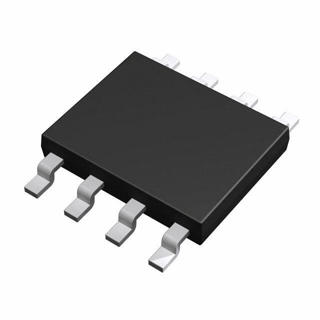
| 描述 | IC VIDEO SIGNAL SWITCHERS 8MSOP |
| 产品分类 | |
| 品牌 | Rohm Semiconductor |
| 数据手册 | |
| 产品图片 |
|
| 产品型号 | BH76332FVM-TR |
| rohs | 无铅 / 符合限制有害物质指令(RoHS)规范要求 |
| 产品系列 | - |
| 供应商器件封装 | 8-MSOP |
| 其它名称 | BH76332FVM-DKR |
| 功能 | 视频开关 |
| 包装 | Digi-Reel® |
| 安装类型 | 表面贴装 |
| 导通电阻 | - |
| 封装/外壳 | 8-VSSOP,8-MSOP(0.110",2.80mm 宽) |
| 工作温度 | -40°C ~ 85°C |
| 标准包装 | 1 |
| 电压-电源,单/双 (±) | 2.8 V ~ 5.5 V |
| 电压源 | 单电源 |
| 电流-电源 | - |
| 电路 | 1 x 3:1 |


- 商务部:美国ITC正式对集成电路等产品启动337调查
- 曝三星4nm工艺存在良率问题 高通将骁龙8 Gen1或转产台积电
- 太阳诱电将投资9.5亿元在常州建新厂生产MLCC 预计2023年完工
- 英特尔发布欧洲新工厂建设计划 深化IDM 2.0 战略
- 台积电先进制程称霸业界 有大客户加持明年业绩稳了
- 达到5530亿美元!SIA预计今年全球半导体销售额将创下新高
- 英特尔拟将自动驾驶子公司Mobileye上市 估值或超500亿美元
- 三星加码芯片和SET,合并消费电子和移动部门,撤换高东真等 CEO
- 三星电子宣布重大人事变动 还合并消费电子和移动部门
- 海关总署:前11个月进口集成电路产品价值2.52万亿元 增长14.8%


PDF Datasheet 数据手册内容提取
High-performance video signal Switcher Series Video Drivers with Built-in Low Voltage operation Single Video Switchers High-performance System video Driver Series Video Drivers with Built-in Input Selection SW BH76330FVM, BH76331FVM, BH76360FV, BH76361FV High-performance video signal Switcher Series Wide Band Low Voltage operation Single Video Switchers BH76332FVM, BH76333FVM, BH76362FV, BH76363FV No.09065EAT01 INDEX Video Drivers with Built-in Low Voltage operation Single Video Switchers BH76330FVM (3input 1output Video Switch)・・・・・・P2 BH76331FVM (3input 1output Video Switch)・・・・・・P2 BH76360FV (6input 1output Video Switch)・・・・・・P17 BH76361FV (6input 1output Video Switch)・・・・・・P17 Wide Band Low Voltage operation Single Video Switchers BH76332FVM (3input 1output Video Switch)・・・・・・P2 BH76333FVM (3input 1output Video Switch)・・・・・・P2 BH76362FV (6input 1output Video Switch)・・・・・・P17 BH76363FV (6input 1output Video Switch)・・・・・・P17 www.rohm.com 1/32 2009.04 - Rev.A © 2009 ROHM Co., Ltd. All rights reserved.
BH76330FVM, BH76331FVM, BH76360FV, BH76361FV, Technical Note BH76332FVM, BH76333FVM, BH76362FV, BH76363FV Line-up of products with built-in video amplifier and video driver 3-input, 1-output video switch BH76330FVM, BH76331FVM, BH76332FVM, BH76333FVM ● General BH76330FVM, BH76331FVM, BH76332FVM, and BH76333FVM are video signal switching ICs, each with three inputs and one circuit input, which feature wide dynamic range and frequency response. Since these ICs can be used with low voltage starting at VCC = 2.8 V, they are applicable not only in stationary devices but also in mobile devices. This product line-up supports a broad range of input signals, depending on whether or not a 6-dB video amplifier and video driver are included and what combination of sync tip clamp type and bias (resistor termination) type inputs are used. ● Features 1) Able to use a wide range of power supply voltage, from 2.8 V to 5.5 V 2) Wide output dynamic range 3) Excellent frequency response (BH76330FVM and BH76331FVM: 100 kHz/10 MHz 0 dB [Typ.], BH76332FVM and BH76333FVM: 100 kHz/30 MHz 0 dB [Typ.]) 4) No crosstalk between channels (Typ. -65 dB, f = 4.43 MHz) 5) Built-in standby function, circuit current during standby is 0 µA (Typ.) 6) Sync tip clamp input (BH76330FVM, BH76332FVM) 7) Bias input (Zin = 150 k) (BH76331FVM, BH76333FVM) 8) 6-dB amp and 75 driver are built in (BH76330FVM, BH76331FVM) 9) Enables two load drivers [when using output coupling capacitor] (BH76330FVM, BH76331FVM) 10) Able to be used without output coupling capacitor (BH76330FVM) 11) MSOP8 compact package ● Applications Input switching in car navigation systems, TVs, DVD systems, etc. ● Line-up BH76330FVM BH76331FVM BH76332FVM BH76333FVM Supply voltage 2.8 V to 5.5 V Amp gain 6 dB -0.1 dB Video driver Included - Frequency response 100 kHz/10 MHz, 0 dB (Typ.) 100 kHz/30 MHz, 0 dB (Typ.) Sync tip Bias Sync tip Bias Input type clamp (Zin = 150 k) clamp (Zin = 150 k) ● Absolute maximum ratings (Ta = 25℃) Parameter Symbol Limits Unit Supply voltage VCC 7.0 V Power dissipation Pd 470 *1 mW Input voltage range V 0 to VCC+0.2 V IN Operating temperature -40 to +85 ℃ Topr range Storage temperature -55 to +125 ℃ Tstg range *1 When used while Ta = 25℃, 4.7 mW is dissipated per 1℃ Mounted on 70 mm x 70 mm x 1.6 mm glass epoxy board ● Operation range (Ta = 25℃) Parameter Symbol Min. Typ. Max Unit Supply voltage VCC 2.8 5.0 5.5 V www.rohm.com 2/32 2009.04 - Rev.A © 2009 ROHM Co., Ltd. All rights reserved.
BH76330FVM, BH76331FVM, BH76360FV, BH76361FV, Technical Note BH76332FVM, BH76333FVM, BH76362FV, BH76363FV ● Electrical characteristics 1 (unless otherwise specified, Ta = 25℃, VCC = 5 V) Typ. Parameter Symbol Unit Conditions 76330 76331 76332 76333 Circuit current 1 ICC1 10 9 mA When no signal Circuit current 2 ICC2 0.0 µA During standby ICC3-1 11 10 During output of color bar signal Circuit current 3 mA During output of color bar signal ICC3-2 17 - (no C in output) Maximum output level VOM 4.6 3.8 3.4 Vpp f = 10 kHz, THD = 1% Voltage gain G 6.0 -0.1 dB Vin = 1.0 Vpp, f = 100 kHz V G 0 - dB Vin = 1.0 Vpp, f = 10 MHz/100 kHz Frequency response F1 G - 0 dB Vin = 1.0 Vpp, f = 30 MHz/100 kHz F2 Crosstalk between C -65 dB Vin = 1.0 Vpp, f = 4.43 MHz channels T Mute attenuation M -65 dB Vin = 1.0 Vpp, f = 4.43 MHz T CTL pin switch level VTHH 1.2 Min V High level threshold voltage VTHL 0.45 Max V Low level threshold voltage CTL pin inflow current I 50 µA CTL pin = 2.0 V applied THH Max Input impedance Zin - 150 - 150 k Differential gain D 0.3 % Vin = 1.0 Vpp G D -1 0.7 0.3 Standard stair step signal P Differential phase deg. Same condition as above D -2 0.0 - P (no C in output) Vin = 1.0 Vpp, bandwidth: 100 k to 6 MHz Y-related S/N SN +75 +78 dB Y 100% white video signal C-related S/N [AM] SNCA +75 dB Vin = 1.0 Vpp, bandwidth: 100 to 500 kHz C-related S/N [PM] SN +65 100% chroma voltage signal CP ● Electrical characteristics 2 (unless otherwise specified, Ta = 25℃, VCC = 3 V) Typ. Parameter Symbol Unit Conditions 76330 76331 76332 76333 Circuit current 1 ICC1 8.5 8.0 mA When no signal Circuit current 2 ICC2 0.0 µA During standby ICC3-1 9.5 9.0 mA During output of color bar signal Circuit current 3 During output of color bar signal ICC3-2 15.5 - (no C in output) Maximum output level VOM 2.7 2.8 1.8 1.9 Vpp f = 10 kHz, THD = 1% Voltage gain G 6.0 -0.1 dB Vin = 1.0 Vpp, f = 100 kHz V G 0 - dB Vin = 1.0 Vpp, f = 10 MHz/100 kHz Frequency response F1 G - 0 dB Vin = 1.0 Vpp, f = 30 MHz/100 kHz F2 Crosstalk between C -65 dB Vin = 1.0 Vpp, f = 4.43 MHz channels T Mute attenuation M -65 dB Vin = 1.0 Vpp, f = 4.43 MHz T CTL pin switch level VTHH 1.2 Min V High level threshold voltage VTHL 0.45 Max V Low level threshold voltage CTL pin inflow current I 50 µA CTL pin = 2.0 V applied THH Max Input impedance Zin - 150 150 k Differential gain D 0.3 0.7 0.3 % Vin = 1.0 Vpp G D -1 1.0 0.3 Standard stair step signal P Differential phase deg. Same condition as above D -2 0.5 - P (no C in output) Vin = 1.0 Vpp, bandwidth: 100 k to 6 MHz Y-related S/N SN +75 +78 dB Y 100% white video signal C-related S/N [AM] SNCA +75 dB Vin = 1.0 Vpp, bandwidth: 100 to 500 kHz C-related S/N [PM] SN +65 dB 100% chroma video signal CP (Note) Re: ICC3, V , G , G , C , M , D , D , SN , SN , and SN parameters OM V F T T G P Y CA CP BH76330FVM and BH76331FVM: RL = 150 BH76332FVM and BH76333FVM: RL = 10 k www.rohm.com 3/32 2009.04 - Rev.A © 2009 ROHM Co., Ltd. All rights reserved.
BH76330FVM, BH76331FVM, BH76360FV, BH76361FV, Technical Note BH76332FVM, BH76333FVM, BH76362FV, BH76363FV ● Control pin settings CTL A B STBY L(OPEN) L(OPEN) IN1 L(OPEN) H IN2 H L(OPEN) IN3 H H ● Block diagram Sync_Tip IN1 Clamp GND IN1 BIAS GND 1 8 1 8 CTLA OUT CTLA OUT 2 6dB 75Ω 7 2 6dB 75Ω 7 Sync_Tip BIAS Clamp IN2 VCC IN2 VCC 3 6 3 6 logic logic Sync_Tip CTLB IN3 CTLB BIAS IN3 Clamp 4 5 4 5 Fig.1 BH76330FV Fig.2 BH76331FV IN1 Sync_Tip GND IN1 BIAS GND Clamp 1 8 1 8 CTLA OUT CTLA OUT 2 0dB 7 2 0dB 7 Sync_Tip BIAS Clamp IN2 VCC IN2 VCC 3 6 3 6 CTLB logic Sync_Tip IN3 CTLB logic BIAS IN3 Clamp 4 5 4 5 Fig. 3 BH76332FV Fig. 4 BH76333FV www.rohm.com 4/32 2009.04 - Rev.A © 2009 ROHM Co., Ltd. All rights reserved.
BH76330FVM, BH76331FVM, BH76360FV, BH76361FV, Technical Note BH76332FVM, BH76333FVM, BH76362FV, BH76363FV ● I/O equivalent circuit diagrams Input pins Sync tip clamp input Bias input BH76330FVM/BH76332FVM BH76331FVM/BH76333FVM Pin No. Name Equivalent circuit Pin No. Name Equivalent circuit 1 IN1 1 IN1 IN 3 IN2 IN 3 IN2 100Ω 100Ω 5 IN3 5 IN3 150kΩ Video signal input pin is used for bias type input. Input Video signal input pin is used for sync tip clamp input. impedance is 150 k. ・DC potential ・DC potential BH76330FVM: 1.5 V BH76332FVM: 1.0 V BH76331FVM: 3.1 V BH76333FVM: 2.5 V Control pins Pin No. Name Equivalent circuit 200kΩ 50kΩ 2 CTLA CTL 4 CTLB 250kΩ 200kΩ Switches operation mode [active or standby] and input pin. Threshold level is 0.45 V to 1.2 V. Output pin With video driver Without video driver BH76330FVM/BH76331FVM BH76332FVM/BH76333FVM Pin No. Name Equivalent circuit Pin No. Name OUT 7 OUT 7 OUT OUT 3.0mA 14kΩ Video signal output pin. Able to drive loads up to 75 Video signal output pin. (dual drive). ・DC potential ・DC potential BH76330FVM: 0.16 V BH76331FVM: 2.5 V BH76332FVM: 0.3 V BH76333FVM: 1.8 V Note 1) The above DC potential is only when VCC = 5 V. This value is a reference value and is not guaranteed. Note 2) Numerical values shown in these figures are design values, and compliance to standards is not guaranteed. www.rohm.com 5/32 2009.04 - Rev.A © 2009 ROHM Co., Ltd. All rights reserved.
BH76330FVM, BH76331FVM, BH76360FV, BH76361FV, Technical Note BH76332FVM, BH76333FVM, BH76362FV, BH76363FV ● Test Circuit Diagrams 0.01μF IN11 SCylanmcp_T ip G8N D 0.01μF IN11 SCylanmcp_T ip G8N D 50Ω CTLA OUT 50Ω CTLA OUT A 2 6dB 75Ω 7 75Ω A 2 0dB 7 0.01μF IN23 SCylanmcp_T ip V6C C10 0.0μ1μF F 75Ω A V V 0.01μF IN23 SCylanmcp_T ip V6C C01.00μ1μFF10kΩ A V V 50Ω A CTL4B logic SCylanmcp_T ip I5N 3 10μF VCC 50Ω A CTL4B logic SCylanmcp_T ip I5N 3 10μF VCC 0.01μF 50Ω 0.01μF50Ω Fig. 5 BH76330FV/BH76331FV Test Circuit Diagram Fig. 6 BH76332FV/BH76333FV Test Circuit Diagram Test circuit diagrams are used for shipment inspections, and differ from application circuits. ● Application circuit examples When used without output capacitor 7 VIDEO_OUT 75Ω IN1 BIAS GND VIDEO_IN 1 8 IN1 SCylanmc_pT ip GND 4.7μF VIDEO_IN 1 8 CTLA OUT 0.1μF 2 6dB 75Ω 7 VIDEO_OUT CTLA OUT BIAS 470μF 75Ω 2 Sync_Tip 6dB 75Ω 7 470μF 75Ω VIDEO_OUT VIDEO_IN IN23 V6C C0.1μF IN2 Clamp VCC 4.7μF logic 47μF VCC VIDEO_IN 0.1μF CTL3B logic SCylanmc_pT ip I6N 3 0.1μF 47μF VCC CTL4B BIAS I5N 3 4.7μF VIDEO_IN 4 5 VIDEO_IN 0.1μF Fig. 7 BH76330FV Fig. 8 BH76331FV Sync_Tip IN1 Clamp GND IN1 BIAS GND VIDEO_IN 1 8 VIDEO_IN 1 8 0.1μF 4.7μF CTLA OUT CTLA OUT 2 0dB 7 VIDEO_OUT 2 0dB 7 VIDEO_OUT Sync_Tip BIAS Clamp VIDEO_IN IN23 V6C C0 .1μF VIDEO_IN IN23 V6C C0.1μF 0.1μF CTLB logic SCylanmcp_T ip IN3 47μF VCC 4.7μF CTLB logic BIAS IN3 47μF VCC 4 5 VIDEO_IN 4 5 VIDEO_IN 0.1μF 4.7μF Fig. 9 BH76332FV Fig. 10 BH76333FV See pages 6/16 to 10/16 for description of how to determine the capacity of I/O coupling capacitors. www.rohm.com 6/32 2009.04 - Rev.A © 2009 ROHM Co., Ltd. All rights reserved.
BH76330FVM, BH76331FVM, BH76360FV, BH76361FV, Technical Note BH76332FVM, BH76333FVM, BH76362FV, BH76363FV ● Cautions for selection and use of application parts When using this IC by itself ① Capacity of input coupling Capacity of output coupling Input impedance Input type capacitor (recommended capacitor (recommended Zin value) value) Sync_Tip_Clamp 10 M 0.1 µF 470 µF to 1000 µF Bias 150 k 4.7 µF Method for determining capacity of input coupling capacitor The HPF is comprised of an input coupling capacitor and the internal input impedance Zin of the IC. Since the fc value of this HPF is determined using the following equation (a), the above recommended capacity for the input capacitor is derived. Usually, the cutoff frequency fc is several Hz. fc = 1 / (2π × C × Zin)・・・・(a) When evaluating the sag characteristics and determining the capacity of the capacitor during video signal input, a horizontal stripe signal called "H bar" (shown in Fig. 10) is suitable, and this type of signal is used instead of a color bar signal to evaluate characteristics and determine capacity. Fig.11 Example of Screen with Obvious Sag (H-bar Signal) Method for determining capacity of output coupling capacitor The output pins of models with a 75 driver [BH76330FVM and BH76331FVM] have an HPF comprised of an output coupling capacitor and load resistance R (= 150). When fc is set to approximately 1 Hz or 2 Hz, the capacity of the output coupling capacitor needs to be L approximately 470 µF to 1000 µF. As for models without the 75 driver, an HPF is similarly comprised using the capacity of the output coupling capacitor and the input impedance of the IC connected at the next stage, and the capacitance required for the output coupling capacitor should be estimated using equation (a). When this IC is used as a standalone device ② In models that include a 75 driver [BH76330FVM and BH76331FVM], up to two monitors (loads) can be connected (a connection example is shown in Fig. 12). When there are multiple loads, the number of output coupling capacitors must be increased or a larger capacitance must be used, based on the table shown below. 470μF monitor (470×2)μF monitor OUT 7 OUT 7 75Ω 75Ω 75Ω 75Ω 470μF monitor monitor 75Ω 75Ω 75Ω 75Ω Fig. 12 (a) Application Circuit Example 1 (Two Drives) Fig. 12 (b) Application Circuit Example 2 (Two Drives) Application circuit example No. of output capacitors Capacitance per output capacitor (recommended values) Fig. 12 (a) No. of drives required 470 µF to 1000 µF (same as with one drive) Fig. 12 (b) 1 (No. of drive × 470 µF to 1000) uF When this IC is used as a standalone device ③ The BH76330FVM is the only model that can be used without an output coupling capacitor. This use method not only enables reductions in board space and part-related costs, but it is able to improve the sag characteristics by improving low-range frequency response. However, when the output coupling capacitor is omitted, a direct current flows to the connected set, so the specifications of the connected set should be noted carefully before starting use. Note also that only one load can be connected when the output coupling capacitor is omitted. monitor OUT 7 Voltage at output ≒0.16V 75Ω W0he2nV this voltage load resistance is applied, 75Ω a direct current is generated. BH76330FV Fig.13 Application Example without Output Coupling Capacitor www.rohm.com 7/32 2009.04 - Rev.A © 2009 ROHM Co., Ltd. All rights reserved.
BH76330FVM, BH76331FVM, BH76360FV, BH76361FV, Technical Note BH76332FVM, BH76333FVM, BH76362FV, BH76363FV When using several of these ICs ① When several of these ICs are used, it enables applications in which separate images are output to the car navigation system's front and rear monitors. Clamp Clamp VIDEO IN IN1 /Bias IN1 /Bias 1 1 Clamp Clamp VIDEO IN IN2 /Bias 470μF Front monitor IN2 /Bias 470μF Rear monitor 3 7 3 7 OUT 75Ω OUT 75Ω Clamp 75Ω Clamp 75Ω VIDEO IN IN3 /Bias IN3 /Bias 5 5 Fig.14 Application Example when Using Several ICs When several ICs are used at the same time, the number of parallel connections of input impedance equals the number of ICs being used, which reduces the input impedance. This also raises the fc value of the HPF formed at the input pin block, so the capacitance of the input coupling capacitor must be increased according to equation (a). The recommended values for calculation results are listed in the table below. When a clamp is used as the input type, the original input impedance becomes much greater, and if two or three are used at the same time there is no need to change the capacitance of the input coupling capacitor. Capacitance of input Number of ICs Total Input type Input impedance per IC coupling capacitor used input impedance (recommended values) 2 Approx. 5 M 0.1 µF Sync_Tip_Clamp Approx. 10 M 3 Approx. 3 M 0.1 µF 2 75 k 6.8 µF~ Bias 150 k 3 50 k 10 µF~ When using several of these ICs ② When three bias input type models (BH76331FVM or BH76333FVM) are used in parallel, they can be used for RGB signal switching applications. Likewise, when one clamp input type model (BH76330FVM or BH76332FVM) is connected in parallel with two bias input type models (a total of three ICs used in parallel), they can be used for component signal switching applications. The same method can be used to determine the capacitance of I/O coupling capacitors of these applications. Bias Clamp VIDEO IN[R1] IN11 BorH B76H373613F3V3F V VIDEO IN[Py1] IN11 BorH B76H373603F3V2F V 4.7μF 0.1uF Bias Clamp VIDEO IN[R2] IN32 O7U T VIDEO IN[Py2] IN32 O7U T 4.7μF Bias R_OUT 0.1uF Clamp Py_OUT VIDEO IN[R3] IN3 VIDEO IN[Py3] IN3 5 5 4.7μF 0.1uF VIDEO IN[G1] IN11 Bias BorH B76H373613F3V3F V VIDEO IN[Pb1] IN11 Bias BorH B76H373613F3V3F V 4.7μF 4.7uF VIDEO IN[G2] IN32 Bias O7U T VIDEO IN[Pb2] IN32 Bias O7U T 4.7μF Bias G_OUT 4.7uF Bias Pb_OUT VIDEO IN[G3] IN3 VIDEO IN[Pb3] IN3 5 5 4.7μF 4.7uF VIDEO IN[B1] IN11 Bias BorH B76H373613F3V3F V VIDEO IN[Pr1] IN11 Bias BorH B76H373613F3V3F V 4.7μF 4.7uF VIDEO IN[B2] IN32 Bias O7U T VIDEO IN[Pr2] IN32 Bias O7U T VIDEO IN[B3] 4.7μF IN3 Bias B_OUT VIDEO IN[Pr3] 4.7uF IN3 Bias Pr_OUT 5 5 4.7μF 4.7uF SW select SW select Fig. 15 (a). RGB Signal Switching Application Example Fig. 15 (b). Component Signal Switching Application Example (using three bias input type models in parallel) (using one clamp input type model and two bias input type models in parallel) www.rohm.com 8/32 2009.04 - Rev.A © 2009 ROHM Co., Ltd. All rights reserved.
BH76330FVM, BH76331FVM, BH76360FV, BH76361FV, Technical Note BH76332FVM, BH76333FVM, BH76362FV, BH76363FV ● Cautions for use 1. The numerical values and data shown here are typical design values, not guaranteed values. 2. The application circuit examples show recommended circuits, but characteristics should be checked carefully before using these circuits. If any external part constants are modified before use, factors such as variation in all external parts and ROHM LSI ICs, including not only static characteristics but also transient characteristics, should be fully considered to set an ample margin. 3. Absolute maximum ratings If the absolute maximum ratings for applied voltage and/or operation temperature are exceeded, LSI damage may result. Therefore, do not apply voltage or use in a temperature that exceeds these absolute maximum ratings. If it is possible that absolute maximum ratings will be exceeded, use a physical safety device such as a fuse and make sure that no conditions that might exceed the absolute maximum ratings will be applied to the LSI IC. 4. GND potential Regardless of the operation mode, the voltage of the GND pin should be at least the minimum voltage. Actually check whether or not the voltage at each pin, including transient phenomena, is less than the GND pin voltage. 5. Thermal design The thermal design should be done using an ample margin that takes into consideration the allowable dissipation under actual use conditions. 6. Shorts between pins and mounting errors When mounting LSI ICs onto the circuit board, make sure each LSI's orientation and position is correct. The ICs may become damaged if they are not mounted correctly when the power is turned on. Similarly, damage may also result if a short occurs, such as when a foreign object is positioned between pins in an IC, or between a pin and a power supply or GND connection. 7. Operation in strong electromagnetic field When used within a strong electromagnetic field, evaluate carefully to avoid the risk of operation faults. 8. Place the power supply's decoupling capacitor as close as possible to the VCC pin (PIN 6) and GND pin (PIN 8). 9. With a clamp input type model (BH76330FVM or BH76332FVM), if any unused input pins are left open they will oscillate, so unused input pins should instead be connected to GND via a capacitor or else directly connected to VCC. 10. With models that do not include a 75driver (BH76332FVM or BH76333FVM), in some cases the capacitance added to the set board may cause the peak frequency response to occur at a high frequency. To lower the peak frequency, connect in series resistors having resistance of several dozen to several hundred as close as possible to the output pin. Output pin OUT 7 Resistors (several dozen Ω to several hundredΩ) to lower peak frequency Fig.16 Positions where Resistors are Inserted to Lower Peak Frequency Response in BH76332FV or BH76333FV 11. Frequency response in models that do not include a 75- driver (BH76332FVM and BH76333FVM) was measured as 100 kH/30 MHz: 0 dB (Typ.) in the application circuit examples (shown in Fig. 9 and Fig. 10), and when resistance of about 1 or 2 k is applied from the IC's output pin to GND, this frequency response can be improved (the lower limit of the applied resistance should be 1 k). In such cases, gain is reduced, since the output voltage is divided by the added resistance and the output resistance of the IC. 1 -0.10 0 -0.12 -1 B] d 3mA OUT 7 Voltage gain [dB] ---432 R=R2=k1ΩkΩ GAIN@f=100kHz[ --00..1164 -5 -0.18 No resistance Resistance to improve frequency -6 response (R: 1-2 kΩ) -0.20 -7 0.5 1 1.5 2 2.5 1M 10M 100M 1000M Resistance added to output pin [k] Frequency [Hz] 出力端子付加抵抗値[kΩ] (a) Resistor insertion points (b) Frequency response changes when resistance is inserted (c) Voltage gain fluctuation when resistance is inserted Input amplitude: 1 Vpp, Output load resistance: 10 kΩ [f = 100 kHz] Other constants are as in application examples (Figs. 9 & 10) (Voltage gain without inserted resistance: -0.11dB) Fig.17 Result of Resistance Inserted to Improve BH76332FVM/BH76333FVM Frequency Response www.rohm.com 9/32 2009.04 - Rev.A © 2009 ROHM Co., Ltd. All rights reserved.
BH76330FVM, BH76331FVM, BH76360FV, BH76361FV, Technical Note BH76332FVM, BH76333FVM, BH76362FV, BH76363FV 12. With clamp input type models (BH76330FVM and BH76332FVM), if the termination impedance of the video input pin becomes higher, sync contractions or oscillation-related problems may occur. Evaluate temperature and other characteristics carefully and use at 1 k or less. 6 unt of sync contraction at input pin [%] 端子でのsync縮み量[%] 2345 mo 力 1 A 入 0 0 1k 2k 3k Input te入rm力in終ati端on抵 re抗siRstian[nΩce] Rin [Ω] Fig. 18. Relation between Input Pin Termination Impedance and Amount of Sync Contraction ● Evaluation board pattern diagram and circuit diagram Fig. 19. Evaluation Board Circuit Diagram Fig. 20. Evaluation Board Pattern Diagram Parts list Symbol Function Recommended value Comments R1 R3 R5 Input terminating resistor 75 - Input coupling C1 C3 C5 See pages 6/16 to 7/16 to determine B characteristics recommended capacitor R71 Output resistor 75 - Output coupling C7 See pages 6/16 to 7/16 to determine B characteristics recommended capacitor C01 10 µF Decoupling capacitor B characteristics recommended C02 0.1 µF www.rohm.com 10/32 2009.04 - Rev.A © 2009 ROHM Co., Ltd. All rights reserved.
BH76330FVM, BH76331FVM, BH76360FV, BH76361FV, Technical Note BH76332FVM, BH76333FVM, BH76362FV, BH76363FV ● Reference data (1) BH76330FVM/BH76331FVM [unless otherwise specified, output capacitance C: 470 µF, RL = 150 BH76330FV Ta=25℃ BH76330FV VCC=5V BH76331FV Ta=25℃ BH76331FV VCC=5V 20 20 20 20 A]mA]15 mA]A]15 A]mA]15 A]mA]15 路電流[mcurrent [10 current [路電流[m10 路電流[mcurrent [10 路電流[mcurrent [10 回Circuit 5 ONou topuuttp cu出出atp c力力aacpiCCtaac容レnitcaス量en cC:e:4 47 700u µFF Circuit 回 5 回Circuit 5 回Circuit 5 0 0 0 0 2 3 4 5 6 -50 0 50 100 2 3 4 5 6 -50 0 50 100 Supp電ly源 V電olt圧ag[eV ][V] Ambie周nt 囲Te温m度pe[r℃atu]re [℃] Supp電ly源 V電olt圧ag[eV ][V] Ambie周nt囲 Te温m度pe[℃rat]ure [℃] Fig. 21 ICC1 vs. Supply Voltage Fig. 22 ICC1 vs. Ambient Temperature Fig. 23 ICC1 vs. Supply Voltage Fig.24 ICC1 vs. Ambient Temperature BH76330/31FV Ta=25℃ BH76330/31FV VCC=5V BH76330FV Ta=25℃ BH76360FV VCC=3V 2.0 2.0 6.0 3.0 回路電流(STBY)[μA]μCircuit current (STBY) [A] 0011....0505 回路電流(STBY)[μA]μCircuit current (STBY) [A] 0011....0505 最大出力レベル[Vpp]Maximum output level [ Vpp] 345...000 最大出力レベル[Vpp]Maximum output level [ Vpp] 2222....2468 -0.5 -0.5 2.0 2.0 2 3 4 5 6 -50 0 50 100 2 3 4 5 6 -50 0 50 100 Sup電pl源y V電o圧lta[gVe] [V] Ambie周nt 囲Te温m度pe[r℃at]ure [℃] Supp電ly源 V電olt圧ag[Ve] [V] Ambie周nt囲 Te温m度pe[r℃at]ure [℃] Fig.25 ICC2 vs. Supply Voltage Fig.26 ICC2 vs. Ambient Temperature Fig.27 Vom vs. Supply Voltage Fig.28 Vom vs. Ambient Temperature BH76331FV Ta=25℃ BH76331FV VCC=3V BH76330FV Ta=25℃ BH76330FV VCC=5V 6.0 3.0 6.3 6.3 aximum output level [ Vpp] 最大出力レベル[Vpp] 345...000 aximum output level [ Vpp] 最大出力レベル[Vpp] 2222....2468 電圧利得[dB]Voltage gain [dB] 55666.....89012 Voltage gain [dB] 電圧利得[dB] 55666.....89012 M 2.0 M 2.0 5.7 5.7 2 3 4 5 6 -50 0 50 100 2 3 4 5 6 -50 0 50 100 Supp電ly源 Vo電lt圧ag[eV []V] Ambie周nt囲 Te温m度pe[℃rat]ure [℃] Supp電ly源 V電olt圧ag[Ve ][V] Ambie周nt囲 Te温m度pe[℃ra]ture [℃] Fig.29 Vom vs. Supply Voltage Fig.30 Vom vs. Ambient Temperature Fig.31 GV vs. Supply Voltage Fig.32 GV vs. Ambient Temperature BH76331FV Ta=25℃ BH76331FV VCC=5V BH76330FV Ta=25℃ BH76330FV VCC=5V 電圧利得[dB]Voltage gain [dB] 5556666.......7890123 2 S3up電ply源 V電o4l圧tag[Ve] [V ]5 6 Voltage gain [dB] 電圧利得[dB] 5556666.......7890123-50 Ambie0周n囲t T温em度p[e℃ra5] t0ure [℃] 100 周波数特性(100k/10MHz)[dB]Frequency response (100 kHz/10 MHz) [dB] ----2110001.......0505050 2 S3upp電ly源 V電o4lt圧ag[eV ][V] 5 6 周波数特性(100k/10MHz)[dB]Frequency response (100 kHz/10 MHz) [dB] ----2110001.......0505050-50 Ambie0周nt囲 Te温m度pe[℃ra5]t0ure [℃] 100 Fig.33 GV vs. Supply Voltage Fig.34 GV vs. Ambient Temperature Fig.35 GF vs. Supply Voltage Fig.36 GF vs. Ambient Temperature www.rohm.com 11/32 2009.04 - Rev.A © 2009 ROHM Co., Ltd. All rights reserved.
BH76330FVM, BH76331FVM, BH76360FV, BH76361FV, Technical Note BH76332FVM, BH76333FVM, BH76362FV, BH76363FV B] BH76331FV Ta=25℃ B] BH76331FV VCC=5V BH76330FV VCC=5V, Ta=25℃ BH76331FV VCC=5V, Ta=25℃ 特性(100k/10MHz)[dB]onse (100 kHz/10 MHz) [d -- 10001.....05050 特性(100k/10MHz)[dB]onse (100 kHz/10 MHz) [d-- 10001.....05050 Gain[dB]-505 Gain[dB]-505 周波数cy resp -1.5 周波数cy resp-1.5 -10 -10 n n ue -2.0 ue-2.0 -15 -15 Freq 2 S3upp電ly 源Vo電l4ta圧ge[V []V] 5 6 Freq -50 Ambien0周t T囲em温p度e[r℃at5u]0re [℃] 100 1M Frequ1e0nMcy[Hz] 100M 1M Frequ1e0nMcy[Hz] 100M Fig.37 GF vs. Supply Voltage Fig.38 GF vs. Ambient Temperature Fig. 39 Frequency Response Fig. 40 Frequency Response sstalk between channels (worst) [dB] チャンネル間クロストーク(worst)[dB]------777666531975 B H76330/31FV Ta=25℃ sstalk between channels (worst) [dB] チャンネル間クロストーク(worst)[dB] ------777666531975 B H76330/31FV VCC=5V ミュート減衰量(worst)[dB]Mute attenuation (worst) [dB] ------877777086420 B H76330/31FV Ta=25℃ ミュート減衰量(worst)[dB]Mute attenuation (worst) [dB] ------877777086420 B H76330/31FV VCC=5V Cro 2 3 4 5 6 Cro -50 0 50 100 2 3 4 5 6 -50 0 50 100 Supp電ly源 V電olt圧ag[eV ][V] Ambien周t T囲em温p度er[a℃tu]re [℃] Supp電ly源 Vo電lta圧g[eV []V] Amb周ien囲t 温Te度m[p℃er]ature [℃] Fig.41 CT(worst) vs. Supply Voltage Fig.42 CT(worst) vs. Ambient Temperature Fig.43 MT(worst) vs. Supply Voltage Fig.44 MT(wrost) vs. Ambient Temperature BH76330/31FV VCC=5V, Ta=25℃ BH76330/31FV VCC=5V BH76330FV Ta=25℃ BH76330FV VCC=5V 20 70 2.0 2.0 回路電流[mA]Circuit current [mA] 11055 CTL_A:0[V] CTL端子流入電流[uA]TL pin influx current [µA] 123456000000 Differential gain [%]微分利得[%] 011...505 Differential gain [%]微分利得[%] 011...505 C 0 0 0.0 0.0 0 0.5 1 1.5 2 -50 0 50 100 2 3 4 5 6 -50 0 50 100 CTCLT_BL _pDin端 v子olt電ag圧e [V] Ambient周 Te囲m温pe度ra[℃tur]e [℃] Sup電p源ly 電Vo圧lta[gVe] [V] Amb電ie源nt 電Te圧m[pVe]rature [℃] F ig. 45 CTLb pin voltage vs Circuit Current Fig.46 ITHH vs. Ambient Temperature Fig.47 DG vs. Supply Voltage Fig.48 DG vs. Ambient Temperature (CLT threshold ) (Voltage applied to CTL pin = 2V) BH76331FV Ta=25℃ BH76331FV VCC=5V BH76330FV Ta=25℃ BH76330FV VCC=5V 2.0 2.0 2.0 2.0 微分利得[%]Differential gain [%] 011...505 Differential gain [%]微分利得[%] 011...505 微分位相[deg.]Differential phase [deg.] 011...505 ONou topuuttp cu出出atp c力力aacpiCCtaaレ容cnitcスa量en cC:e:4 47700u FµF Differential phase [deg.]微分位相[deg.] 011...505 ONou topuuttp 出出cuatp力力 caacCCpita容レacniス量tcaen: cC4e:7 407u0F µF 0.0 0.0 0.0 0.0 2 Su3pp電ly源 V電olt4圧ag[eV ][V] 5 6 -50 Ambien電0t T源e電mp圧er[aVtu5]r0e [℃] 100 2 3Sup電p源ly 電V4o圧lta[Vg]e [V]5 6 -50 Ambie電n0t 源Te電m圧pe[rVa]5tu0re [℃] 100 Fig.49 DG vs. Supply Voltage Fig.50 DG vs. Ambient Temperature Fig.51 DP vs. Supply Voltage Fig.52 DP vs. Ambient Temperature www.rohm.com 12/32 2009.04 - Rev.A © 2009 ROHM Co., Ltd. All rights reserved.
BH76330FVM, BH76331FVM, BH76360FV, BH76361FV, Technical Note BH76332FVM, BH76333FVM, BH76362FV, BH76363FV BH76331FV Ta=25℃ BH76331FV VCC=5V BH76330/31FV Ta=25℃ BH76330/31FV VCC=5V 2.0 2.0 80 80 eg.] 1.5 eg.] 1.5 78 78 微分位相[deg.]Differential phase [d 01..50 Differential phase [d微分位相[deg.] 01..50 Y系S/N[dB]Y S/N [dB] 777246 Y S/N [dB]Y系S/N[dB] 777246 0.0 0.0 70 70 2 3 4 5 6 -50 0 50 100 2 3 4 5 6 -50 0 50 100 Suppl電y V源o電lta圧ge[V [V]] Ambient電 Te源m電pe圧ra[tVu]re [℃] Sup電ply源 V電olt圧ag[eV []V] Ambie周nt囲 Te温m度pe[r℃atu]re [℃] Fig.53 DP vs. Supply Voltage Fig.54 DP vs. Ambient Temperature Fig.55 SNY vs. Supply Voltage Fig.56 SNY vs. Ambient Temperature BH76330/31FV Ta=25℃ BH76330/31FV VCC=5V BH76330/31FV Ta=25℃ BH76330/31FV VCC=5V 80 80 70 70 78 78 69 69 C S/N (AM) [dB]C系S/N(AM)[dB]777246 C系S/N(AM)[dB]C S/N (AM) [dB] 777246 C系S/N(PM)[dB]C S/N (PM) [dB] 666678 C系S/N(PM)[dB]C S/N (PM) [dB] 666678 70 70 65 65 2 3 4 5 6 -50 0 50 100 2 3 4 5 6 -50 0 50 100 Supp電ly 源Vo電lta圧g[eV []V] Ambien周t T囲em温pe度ra[t℃ur]e [℃] Sup電pl源y V電ol圧tag[eV ][V] Ambie周nt囲 Te温m度pe[r℃atu]re [℃] Fig.57 SNCA vs. Supply Voltage Fig.58 SNCA vs. Ambient Temperature Fig.59 SNCP vs. Supply Voltage Fig.60 SNCP vs. Ambient Temperature ● Reference data (2) BH76332FVM/BH76333FVM [unless otherwise specified, output capacitance C: 470 µF, RL = 10 k] BH76332FV Ta=25℃ BH76332FV VCC=5V BH76333FV Ta=25℃ BH76333FV VCC=5V 20 20 20 20 ent [mA]流[mA]1105 流[mA]ent [mA]1105 ent [mA]流[mA]1105 ent [mA]流[mA]1105 urr電 電urr urr電 urr電 Circuit c回路 5 回路Circuit c 5 Circuit c回路 5 Circuit c回路 5 0 0 0 0 2 3 4 5 6 -50 0 50 100 2 3 4 5 6 -50 0 50 100 Sup電ply源 V電olt圧ag[eV []V] Ambie周nt囲 Te温mp度er[a℃tu]re [℃] Sup電pl源y V電ol圧tag[eV ][V] Ambie周nt囲 Te温m度pe[ra℃tu]re [℃] Fig.61 ICC1 vs. Supply Voltage Fig.62 ICC1 vs. Ambient Temperature Fig.63 ICC1 vs. Supply Voltage Fig.64 ICC1 vs. Ambient Temperature BH76332/33FV Ta=25℃ BH76332/33FV VCC=5V BH76332FV Ta=25℃ BH76332FV VCC=3V 2.0 2.0 5.0 2.5 μCircuit current (STBY) [A]回路電流(STBY)[μA] 0011....0505 μCircuit current (STBY) [A]回路電流(STBY)[μA] 0011....0505 Maximum output level [ Vpp] 最大出力レベル[Vpp] 234...000 最大出力レベル[Vpp]Maximum output level [ Vpp] 1122....7913 -0.5 -0.5 1.0 1.5 2 3 4 5 6 -50 0 50 100 2 3 4 5 6 -50 0 50 100 Sup電pl源y V電o圧lta[gVe] [V] Ambien周t T囲em温p度er[a℃tu]re [℃] Sup電ply源 V電ol圧tag[Ve ][V] Ambien周t 囲Te温mp度e[ra℃tu]re [℃] Fig.65 ICC2 vs. Supply Voltage Fig.66 ICC2 vs. Ambient Temperature Fig.67 Vom vs. Supply Voltage Fig.68 Vom vs. Ambient Temperature www.rohm.com 13/32 2009.04 - Rev.A © 2009 ROHM Co., Ltd. All rights reserved.
BH76330FVM, BH76331FVM, BH76360FV, BH76361FV, Technical Note BH76332FVM, BH76333FVM, BH76362FV, BH76363FV BH76333FV Ta=25℃ BH76333FV VCC=3V BH76332FV Ta=25℃ BH76332FV VCC=5V 5.0 2.5 0.4 0.4 p] p] ximum output level [ Vp最大出力レベル[Vpp] 234...000 最大出力レベル[Vpp]ximum output level [ Vp 1122....7913 Voltage gain [dB] 電圧利得[dB]--0000....0242 Voltage gain [dB] 電圧利得[dB]--0000....4202 a a M M 1.0 1.5 -0.6 -0.6 2 3 4 5 6 -50 0 50 100 2 3 4 5 6 -50 0 50 100 Supp電ly源 Vo電lta圧g[eV []V] Ambien周t T囲e温mp度er[a℃tu]re [℃] Suppl電y V源o電lta圧ge[V []V] Ambien周t T囲em温p度er[a℃tu]re [℃] Fig.69 Vom vs. Supply Voltage Fig.70 Vom vs. Ambient Temperature Fig.71 GV vs. Supply Voltage Fig.72 GV vs. Ambient Temperature BH76333FV Ta=25℃ BH76333FV VCC=5V dB] BH76332FV Ta=25℃ dB] BH76332FV VCC=5V 0.4 0.4 Hz) [ 1.0 Hz) [ 1.0 MB] B]M Voltage gain [dB] 電圧利得[dB]--0000....4202 Voltage gain [dB] 電圧利得[dB]--0000....0242 cy response (100 kHz/10 波数特性(100k/30MHz)[d---11000.....05505 波数特性(100k/30MHz)[dcy response (100 kHz/10 ---11000.....50505 -0.6 -0.6 uen周-2.0 周uen-2.0 q q 2 3 4 5 6 -50 0 50 100 Fre 2 3 4 5 6 Fre -50 0 50 100 Supp電ly源 V電olt圧ag[eV ][V] Ambie周nt 囲Te温mp度er[a℃tu]re [℃] Supp電ly源 V電olt圧ag[eV []V] Amb周ien囲t T温em度pe[℃rat]ure [℃] Fig.73 GV vs. Supply Voltage Fig.74 GV vs. Ambient Temperature Fig.75 GF vs. Supply Voltage Fig.76 GF vs. Ambient Temperature dB] BH76333FV Ta=25℃ dB] BH76333FV VCC=5V BH76332FV VCC=5V ,Ta=25℃ BH76333FV VCC=5V ,Ta=25℃ onse (100 kHz/10 MHz) [性(100k/30MHz)[dB]--00110.....05005 性(100k/30MHz)[dB]onse (100 kHz/10 MHz) [--00110.....05050 Gain[dB]--01221 Gain[dB]--21012 sp特 特sp -3 -3 cy re波数-1.5 波数cy re-1.5 -4 -4 quen周-2.0 周quen-2.0 -5 -5 Fre 2 Su3pp電ly源 Vo電l4ta圧g[eV []V] 5 6 Fre -50 Amb周ie0n囲t T温em度p[e℃ra5t]0ure [℃] 100 1M Freq1u0eMncy[Hz] 100M 1M Freq1u0eMncy[Hz] 100M Fig.77 G vs. Supply Voltage Fig.78 G vs. Ambient Temperature Fig. 79 Frequency Response Fig. 80 Frequency Response F F BH76332/33FV Ta=25℃ BH76332/33FV VCC=5V BH76332/33FV Ta=25℃ BH76332/33FV VCC=5V Crosstalk between channels (worst) [dB] チャンネル間クロストーク(worst)[dB]------777666531975 2 S3upp電ly源 V電o4lt圧ag[eV ][V] 5 6 チャンネル間クロストーク(worst)[dB]Crosstalk between channels (worst) [dB] ------777666531975-50 Ambie0周n囲t T温em度p[e ℃ra5]t0ure [℃] 100 Mute attenuation (worst) [dB] ミュート減衰量(worst)[dB]------877777086420 2 3Sup電ply源 V4電olt圧ag[eV ][V5] 6 ミュート減衰量(worst)[dB]Mute attenuation (worst) [dB] ------877777086420-50 Amb0周ie囲nt 温Te度m[p℃e5r]0a ture [℃]100 Fig.81 CT(worst) vs. Supply Voltage Fig.82 CT(worst) vs. Ambient Temperature Fig.83 MT(worst) vs. Supply Voltage Fig.84 MT(wrost) vs. Ambient Temperature www.rohm.com 14/32 2009.04 - Rev.A © 2009 ROHM Co., Ltd. All rights reserved.
BH76330FVM, BH76331FVM, BH76360FV, BH76361FV, Technical Note BH76332FVM, BH76333FVM, BH76362FV, BH76363FV BH76332/33FV VCC=5V, Ta=25℃ BH76332/33FV VCC=5V BH76332FV Ta=25℃ BH76332FV VCC=5V 20 70 2.0 2.0 Circuit current [mA] 回路電流[mA]11505 CTL_A:0[V] TL pin influx current [µA]CTL端子流入電流[uA] 123456000000 微分利得[%]Differential gain [%] 011...505 微分利得[%]Differential gain [%] 011...505 C 0 0 0 0.5 1 1.5 2 -50 0 50 100 0.0 0.0 CTLC_TBL p_Din端 vo子lta電ge圧 [V] Ambie周nt 囲Te温m度pe[r℃at]ure [℃] 2 S3u電pp源ly V電o4圧lta[gVe] [V]5 6 -50 Amb電i0en源t T電em圧p[eVra]5t0ure [℃] 100 Fig .85 CTLb( CpiLnT v tohlrtaegsheo vlds C) ircuit Current Fig(V.8o6lt agITeH Ha pvpsl.i eAdm tboi eCnTt LT epminp =e r2aVtu) re Fig.87 DG vs. Supply Voltage Fig.88 DG vs. Ambient Temperature BH76333FV Ta=25℃ BH76333FV VCC=5V BH76332FV Ta=25℃ BH76332FV VCC=5V 2.0 2.0 2.0 2.0 %] 1.5 %] 1.5 eg.] 1.5 eg.] 1.5 Differential gain [微分利得[%] 01..50 微分利得[%]Differential gain [ 01..50 微分位相[deg.]erential phase [d 01..50 微分位相[deg.]erential phase [d 01..50 Diff Diff 0.0 0.0 0.0 0.0 2 3 4 5 6 -50 0 50 100 2 3 4 5 6 -50 0 50 100 Supp電ly源 V電olt圧ag[eV ][V] Ambie電nt 源Te電mp圧e[raVt]ure [℃] Sup電ply源 V電ol圧tag[Ve] [V] Ambie電nt 源Te電m圧pe[rVa]ture [℃] Fig.89 DG vs. Supply Voltage Fig.90 DG vs. Ambient Temperature Fig.91 DP vs. Supply Voltage Fig.92 DP vs. Ambient Temperature BH76333FV Ta=25℃ BH76333FV VCC=5V BH76332/33FV Ta=25℃ BH76332/33FV VCC=5V 2.0 2.0 80 80 eg.] 1.5 eg.] 1.5 78 78 Differential phase [d微分位相[deg.] 01..50 微分位相[deg.]Differential phase [d 01..50 Y S/N [dB]Y系S/N[dB] 777246 Y系S/N[dB]Y S/N [dB] 777246 0.0 0.0 70 70 2 3 4 5 6 -50 0 50 100 2 3 4 5 6 -50 0 50 100 Supp電ly源 Vo電lt圧ag[eV ][V] Ambien電t T源em電p圧er[aVt]ure [℃] Suppl電y 源Vo電lta圧ge[V []V] Ambi周en囲t T温em度p[℃era]ture [℃] Fig.93 DP vs. Supply Voltage Fig.94 DP vs. Ambient Temperature Fig.95 SNY vs. Supply Voltage Fig.96 SNY vs. Ambient Temperature BH76332/33FV Ta=25℃ BH76332/33FV VCC=5V BH76332/33FV Ta=25℃ BH76332/33FV VCC=5V 80 80 70 70 78 78 69 69 C S/N (AM) [dB]C系S/N(AM)[dB]777246 C S/N (AM) [dB]C系S/N(AM)[dB] 777246 C系S/N(PM)[dB]C S/N (PM) [dB] 666678 C系S/N(PM)[dB]C S/N (PM) [dB] 666678 70 70 65 65 2 3 4 5 6 -50 0 50 100 2 3 4 5 6 -50 0 50 100 Supp電ly 源Vo電lta圧ge[V []V] Ambien周t T囲em温p度era[℃tur]e [℃] Supp電ly源 Vo電lta圧ge[V [V]] Amb周ien囲t T温em度p[e℃ra]ture [℃] Fig.97 SNCA vs. Supply Voltage Fig.98 SNCA vs. Ambient Temperature Fig.99 SNCP vs. Supply Voltage Fig.100 SNCP vs. Ambient Temperature www.rohm.com 15/32 2009.04 - Rev.A © 2009 ROHM Co., Ltd. All rights reserved.
BH76330FVM, BH76331FVM, BH76360FV, BH76361FV, Technical Note BH76332FVM, BH76333FVM, BH76362FV, BH76363FV ● External dimensions and label codes Max 3.25 (include . BURR) 7 6 3 3 0 Model Code BH76330FV 76330 BH76331FV 76331 BH76332FV 76332 Lot. No. BH76333FV 76333 MSOP8 (unit: mm ) Fig. 101 External Dimensions of BH7633xFVM Series Package ● When used with 6-input, 1-output video switch BH7636xFV Fig. 14 above shows an application example in which two of these ICs are used. When the similar IC models BH7636xFV and BH7633xFVM are used at the same time, the type of configuration shown below can be combined. In such cases, input coupling capacitors can be used, as in the application example in Fig. 14. ※1 BH76360FV IIN1 Clamp Exter外na部l i入np力ut 2 IIN2 Clamp ※2 フロンFrトoモntニ タ TV 4 16 monitor OUT 75Ω 75Ω IIN3 Clamp *1 Input coupling capacitor can be used with DVD 6 this. IIN4 Clamp Nasナvciビrgea画etni面o n 8 *2 Output coupling capacitors can be omitted when using BH76330FVM or BH76360FV, IIN5 Clamp and this helps reduce the number of parts. Reaリr アcaカmメeラra 9 IIN6 Clamp *3 Any inputs that are not used should be ※3 11 connected directly to VCC or shorted with GND via a capacitor. BH76330FVM IIN1 Clamp 1 IIN2 Clamp ※2 リアモRニeタar 3 16 monitor OUT 75Ω 75Ω IIN3 Clamp 5 Fig. 102 Application Example in which BH76330FVM and BH76360FV Are Used Concurrently For details of BH7636xFV, see the BH7636xFV Series Application Notes. www.rohm.com 16/32 2009.04 - Rev.A © 2009 ROHM Co., Ltd. All rights reserved.
BH76330FVM, BH76331FVM, BH76360FV, BH76361FV, Technical Note BH76332FVM, BH76333FVM, BH76362FV, BH76363FV Line-up of products with built-in video amplifier and video driver 6-input, 1-output video switch BH76360FV, BH76361FV, BH76362FV, BH76363FV ●General BH76360FV, BH76361FV, BH76362FV, and BH76363FV are video signal switching ICs, each with six inputs and one circuit input, which feature wide dynamic range and frequency response. Since these ICs can be used with low voltage starting at VCC = 2.8 V, they are applicable not only in stationary devices but also in mobile devices. This product line-up supports a broad range of input signals, depending on whether or not a 6-dB video amplifier and video driver are included and what combination of sync tip clamp type and bias (resistor termination) type inputs are used. ●Features 1) Able to use a wide range of power supply voltage, from 2.8 V to 5.5 V 2) Wide output dynamic range 3) Excellent frequency response (BH76360FV, BH76361FV:100kHz/10MHz 0dB[Typ.]、BH76362FV, BH76363FV:100kHz/30MHz 0dB[Typ.]) 4) No crosstalk between channels (Typ.-65dB, f=4.43MHz) 5) Built-in mute function (Typ.-65dB, f=4.43MHz) 6) Built-in standby function, circuit current during standby is 0 µA (Typ.) 7) Sync tip clamp input (BH76360FV, BH76362FV) 8) Bias input (Zin=150kΩ) (BH76361FV, BH76363FV) 9) 6-dB amp and 75 driver are built in (BH76360FV, BH76361FV) 10) Enables two load drivers [when using output coupling capacitor](BH76360FV, BH76361FV) 11) Able to be used without output coupling capacitor (BH76360FV) 12) SSOP-B16 compact package ●Applications Input switching in car navigation systems, TVs, DVD systems, etc. ●Line-up BH76360FV BH76361FV BH76362FV BH76363FV Supply voltage 2.8 V to 5.5 V Amp gain 6dB -0.1dB Video driver Included - Frequency response 100kHz/10MHz 0dB (Typ.) 100kHz/30MHz 0dB (Typ.) Sync tip Bias Sync tip Bias Input type clamp (Zin = 150 k) clamp (Zin = 150 k) ●Absolute maximum ratings (Ta = 25℃) Parameter Symbol Limits Unit Supply voltage VCC 7.0 V Power dissipation Pd 450 *1 mW Input voltage range V 0 to VCC+0.2 V IN Operating temperature -40 to +85 ℃ Topr range Storage temperature -55 to +125 ℃ Tstg range *1 When used while Ta = 25℃, 4.7 mW is dissipated per 1℃ Mounted on 70 mm x 70 mm x 1.6 mm glass epoxy board ●Operation range (Ta = 25℃) Parameter Symbol Min. Typ. Max Unit Supply voltage VCC 2.8 5.0 5.5 V www.rohm.com 17/32 2009.04 - Rev.A © 2009 ROHM Co., Ltd. All rights reserved.
BH76330FVM, BH76331FVM, BH76360FV, BH76361FV, Technical Note BH76332FVM, BH76333FVM, BH76362FV, BH76363FV ●Electrical characteristics 1 (unless otherwise specified, Ta=25℃、VCC=5V) Typ. Parameter Symbol Unit Conditions 76360 76361 76362 76363 Circuit current 1 ICC1 12 11 mA When no signal Circuit current 2 ICC2 0.0 uA During standby ICC3-1 13 12 During output of color bar signal Circuit current 3 mA During output of color bar signal ICC3-2 19 - (no C in output) Maximum output level VOM 4.6 3.8 3.4 Vpp f=10kHz, THD=1% Voltage gain G 6.0 -0.1 dB Vin=1.0Vpp, f=100kHz V G 0 - dB Vin=1.0Vpp, f=10MHz/100kHz Frequency response F1 G - 0 dB Vin=1.0Vpp, f=30MHz/100kHz F2 Crosstalk between C -65 dB Vin=1.0Vpp, f=4.43MHz channels T Mute attenuation M -65 dB Vin=1.0Vpp, f=4.43MHz T CTL pin switch level VTHH 1.2 Min V High Level threshold voltage VTHL 0.45 Max V Low Level threshold voltage CTL pin inflow current I 50 uA CTL pin = 2.0 V applied THH Max Input impedance Zin - 150 - 150 kΩ Differential gain D 0.3 % Vin=1.0Vpp G D -1 0.7 0.3 Standard stair step signal Differential phase P deg. DP-2 0.0 - Same condition as above (no C in output) Vin = 1.0 Vpp, bandwidth: 100 k to 6 MHz Y-related S/N SN +75 +78 dB Y 100% white video signal C-related S/N [AM] SNCA +75 dB Vin = 1.0 Vpp, bandwidth: 100 to 500 kHz C-related S/N [PM] SNCP +65 100% chroma voltage signal ●Electrical characteristics 2 (unless otherwise specified, Ta = 25℃, VCC = 3 V) Typ. Parameter Symbol Unit Conditions 76360 76361 76362 76363 Circuit current 1 ICC1 10 mA When no signal Circuit current 2 ICC2 0.0 uA During standby ICC3-1 11 10 mA During output of color bar signal Circuit current 3 During output of color bar signal ICC3-2 17 - (no C in output) Maximum output level VOM 2.7 2.8 1.8 1.9 Vpp f=10kHz, THD=1% Voltage gain G 6.0 -0.1 dB Vin=1.0Vpp, f=100kHz V G 0 - dB Vin=1.0Vpp, f=10MHz/100kHz Frequency response F1 G - 0 dB Vin=1.0Vpp, f=30MHz/100kHz F2 Crosstalk between C -65 dB Vin=1.0Vpp, f=4.43MHz channels T Mute attenuation M -65 dB Vin=1.0Vpp, f=4.43MHz T CTL pin switch level VTHH 1.2 Min V High Level threshold voltage VTHL 0.45 Max V Low Level threshold voltage CTL pin inflow current I 50 uA CTL pin = 2.0 V applied THH Max Input impedance Zin - 150 - 150 kΩ Differential gain D 0.3 % Vin=1.0Vpp G D -1 1.0 0.3 Standard stair step signal Differential phase P deg. DP-2 0.5 - Same condition as above (no C in output) Vin = 1.0 Vpp, bandwidth: 100 k to 6 MHz Y-related S/N SN +75 +78 dB Y 100% white video signal C-related S/N [AM] SNCA +75 dB Vin = 1.0 Vpp, bandwidth: 100 to 500 kHz C-related S/N [PM] SNCP +65 dB 100% chroma video signal (Note) Re: ICC3, V , G , G , C , M , D , D , SN , SN , SN parameters OM V F T T G P Y CA CP BH76360FV, BH76361FV: RL = 150 BH76362FV, BH76363FV: RL = 10 k www.rohm.com 18/32 2009.04 - Rev.A © 2009 ROHM Co., Ltd. All rights reserved.
BH76330FVM, BH76331FVM, BH76360FV, BH76361FV, Technical Note BH76332FVM, BH76333FVM, BH76362FV, BH76363FV ●Control pin settings CTLA CTLB CTLC CTLD IN1 L(OPEN) L(OPEN) L(OPEN) H IN2 H L(OPEN) L(OPEN) H IN3 L(OPEN) H L(OPEN) H IN4 H H L(OPEN) H IN5 L(OPEN) L(OPEN) H H IN6 H L(OPEN) H H MUTE * H H H STBY * * * L(OPEN) * L(OPEN) or H either is possible ●Block diagram IN4 GND IN3 GND IN2 VCC IN1 PVCC IN4 GND IN3 GND IN2 VCC IN1 PVCC 8 7 6 5 4 3 2 1 8 7 6 5 4 3 2 1 Sync_Tip Sync_Tip Sync_Tip Sync_Tip BIAS BIAS BIAS BIAS Clamp Clamp Clamp Clamp 6dB 75Ω 6dB 75Ω logic logic Sync_Tip Sync_Tip Clamp Clamp BIAS BIAS 9 10 11 12 13 14 15 16 9 10 11 12 13 14 15 16 IN5 CTLA IN6 CTLB CTLC CTLD PGND OUT IN5 CTLA IN6 CTLB CTLC CTLD PGND OUT Fig.1 BH76360FV Fig.2 BH76361FV IN4 GND IN3 GND IN2 VCC IN1 PVCC IN4 GND IN3 GND IN2 VCC IN1 PVCC 8 7 6 5 4 3 2 1 8 7 6 5 4 3 2 1 Sync_Tip Sync_Tip Sync_Tip Sync_Tip BIAS BIAS BIAS BIAS Clamp Clamp Clamp Clamp 0dB 0dB logic logic SCylanmcp_T ip SCylanmc_pT ip BIAS BIAS 9 10 11 12 13 14 15 16 9 10 11 12 13 14 15 16 IN5 CTLA IN6 CTLB CTLC CTLD PGND OUT IN5 CTLA IN6 CTLB CTLC CTLD PGND OUT Fig.3 BH76362FV Fig.4 BH76363FV www.rohm.com 19/32 2009.04 - Rev.A © 2009 ROHM Co., Ltd. All rights reserved.
BH76330FVM, BH76331FVM, BH76360FV, BH76361FV, Technical Note BH76332FVM, BH76333FVM, BH76362FV, BH76363FV ●I/O equivalent circuit diagrams Input pins Sync tip clamp input Bias input BH76360FV / BH76362FV BH76361FV / BH76363FV PIN No. Name Equivalent circuit PIN No. Name Equivalent circuit 2 IN1 2 IN1 4 IN2 4 IN2 6 IN3 6 IN3 IN IN 8 IN4 100Ω 8 IN4 100Ω 9 IN5 9 IN5 150kΩ 11 IN6 11 IN6 Video signal input pin is used for bias type input. Input Video signal input pin is used for sync tip clamp input. impedance is 150 k. ・DC potential ・DC potential BH76360FV:1.5V BH76362FV :1.0V BH76361FV:3.1V BH76363FV :2.5V Control pins PIN No. Name Equivalent circuit 200kΩ 10 CTLA 50kΩ 12 CTLB CTL 13 CTLC 250kΩ 14 CTLD 200kΩ Switches operation mode [active or standby] and input pin. Threshold level is 0.45 V to 1.2 V. Output pin With video driver Without video driver BH76360FV / BH76361FV BH76362FV / BH76363FV PIN No. Name Equivalent circuit PIN No. Name OUT 16 OUT 16 OUT OUT 3.0mA 14kΩ Video signal output pin. Able to drive loads up to 75 Video signal output pin. (dual drive). ・DC potential ・DC potential BH76360FV:0.16V BH76361FV:2.5V BH76362FV:0.3V BH76363FV :1.8V Note 1) The above DC potential is only when VCC = 5 V. This value is a reference value and is not guaranteed. Note 2) Numerical values shown in these figures are design values, and compliance to standards is not guaranteed. www.rohm.com 20/32 2009.04 - Rev.A © 2009 ROHM Co., Ltd. All rights reserved.
BH76330FVM, BH76331FVM, BH76360FV, BH76361FV, Technical Note BH76332FVM, BH76333FVM, BH76362FV, BH76363FV ●Test Circuit Diagrams A 10μF 0.01μF A 10μF 0.01μF PVCC OUT 75Ω PVCC OUT VVCCCC 1 16 VVCCCC 1 16 0.01μF IN1 ClamBpia/s PGND 10μF75Ω V V 0.01μF IN1 ClamBpia/s PGND10μF10kΩ V V 2 15 2 15 50Ω 75Ω 50Ω VCC CTLD VCC CTLD 3 14 A 3 0dB 14 A Clamp/ 6dB Clamp/ 0.01μF IN2 Bias CTLC 0.01μF IN2 Bias CTLC 4 13 A 4 13 A 50Ω 50Ω GND CTLB GND CTLB 5 logic 12 A 5 logic 12 A Clamp/ Clamp/ Clamp/ Clamp/ 0.01μF IN3 Bias Bias IN6 0.01μF 0.01μF IN3 Bias Bias IN6 0.01μF 6 11 6 11 50Ω 50Ω 50Ω 50Ω GND CTLA GND CTLA 7 10 A 7 10 A Clamp/ Clamp/ Clamp/ Clamp/ 0.01μF IN4 Bias Bias IN5 0.01μF 0.01μF IN4 Bias Bias IN5 0.01μF 8 9 8 9 50Ω 50Ω 50Ω 50Ω Fig.5 BH76360FV/BH76361FV Test Circuit Diagram Fig.6 BH76362FV/BH76363FV Test Circuit Diagram Test circuit diagrams are used for shipment inspections, and differ from application circuits. ● Application circuit examples 出力コンデンサレス OUT で使用する場合 16 10μF 0.1μF 75Ω VIDEO_OUT 10μF 0.1μF VCC PVCC OUT 470μF VCC PVCC OUT 470μF 1 16 1 16 75Ω VIDEO_OUT 75Ω VIDEO_OUT IN1 SCylanmcp_T ip PGND IN1 BIAS PGND VIDEO_IN 0.1μF 2 75Ω 15 VIDEO_IN 4.7μF 2 75Ω 15 VC3C C1T4L D VC3C C1T4LD IN2 SCylanmcp_T ip 6dB CTLC IN2 BIAS 6dB CTLC VIDEO_IN 4 13 VIDEO_IN 4 13 0.1μF 4.7μF GND CTLB GND CTLB 5 logic 12 5 logic 12 IN3 SCylanmcp_T ip SCylanmc_pT ip IN6 0.1μF IN3 BIAS BIAS IN6 4.7μF VIDEO_IN 6 11 VIDEO_IN VIDEO_IN 6 11 VIDEO_IN 0.1μF 4.7μF GND CTLA GND CTLA 7 10 7 10 IN4 SCylanmcp_T ip SCylanmc_pT ip IN5 0.1μF IN4 BIAS BIAS IN5 4.7μF VIDEO_IN 8 9 VIDEO_IN VIDEO_IN 8 9 VIDEO_IN 0.1μF 4.7μF Fig.7 BH76360FV Fig.8 BH76361FV 10μF 0.1μF 10μF 0.1μF VCC PVCC OUT VCC PVCC OUT 1 16 1 16 VIDEO_OUT Sync_Tip VIDEO_OUT IN1 Clamp PGND IN1 BIAS PGND VIDEO_IN 2 15 VIDEO_IN 2 15 0.1μF 4.7μF VCC CTLD VCC CTLD 3 0dB 14 3 0dB 14 IN2 SCylanmcp_T ip CTLC IN2 BIAS CTLC VIDEO_IN 4 13 VIDEO_IN 4 13 0.1μF 4.7μF GND CTLB GND CTLB 5 logic 12 5 logic 12 Sync_Tip Sync_Tip IN3 Clamp Clamp IN6 0.1μF IN3 BIAS BIAS IN6 4.7μF VIDEO_IN 6 11 VIDEO_IN VIDEO_IN 6 11 VIDEO_IN 0.1μF 4.7μF GND CTLA GND CTLA 7 10 7 10 Sync_Tip Sync_Tip VIDEO_IN IN84 Clamp Clamp IN95 0.1μF VIDEO_IN VIDEO_IN IN84 BIAS BIAS IN95 4.7μF VIDEO_IN 0.1μF 4.7μF Fig.9 BH76362FV Fig.10 BH76363FV See pages 6/16 to 10/16 for description of how to determine the capacity of I/O coupling capacitors. www.rohm.com 21/32 2009.04 - Rev.A © 2009 ROHM Co., Ltd. All rights reserved.
BH76330FVM, BH76331FVM, BH76360FV, BH76361FV, Technical Note BH76332FVM, BH76333FVM, BH76362FV, BH76363FV ●Cautions for selection and use of application parts When using this IC by itself ① Input impedance Capacity of input coupling Capacity of output coupling Input type Zin capacitor (recommended value) capacitor (recommended value) Sync_Tip_Clamp 10MΩ 0.1uF 470uF~1000uF Bias 150kΩ 4.7uF Method for determining capacity of input coupling capacitor The HPF is comprised of an input coupling capacitor and the internal input impedance Zin of the IC. Since the fc value of this HPF is determined using the following equation (a), the above recommended capacity for the input capacitor is derived. Usually, the cutoff frequency fc is several Hz. fc = 1 / (2π × C × Zin)・・・・(a) When evaluating the sag characteristics and determining the capacity of the capacitor during video signal input, a horizontal stripe signal called "H bar" (shown in Fig. 10) is suitable, and this type of signal is used instead of a color bar signal to evaluate characteristics and determine capacity. Fig.11 Example of Screen with Obvious Sag (H-bar Signal) Method for determining capacity of output coupling capacitor The output pins of models with a 75 driver [BH76360FV and BH76361FV] have an HPF comprised of an output coupling capacitor and load resistance R (= 150). When fc is set to approximately 1 Hz or 2 Hz, the capacity of the output coupling capacitor needs to be L approximately 470 µF to 1000 µF. As for models without the 75 driver, an HPF is similarly comprised using the capacity of the output coupling capacitor and the input impedance of the IC connected at the next stage, and the capacitance required for the output coupling capacitor should be estimated using equation (a). When this IC is used as a standalone device ② In models that include a 75 driver [BH76360FV and BH76361FV], up to two monitors (loads) can be connected (a connection example is shown in Fig. 12). When there are multiple loads, the number of output coupling capacitors must be increased or a larger capacitance must be used, based on the table shown below. 470μF monitor (470×2)μF monitor OUT 16 OUT 16 75Ω 75Ω 75Ω 75Ω 470μF monitor monitor 75Ω 75Ω 75Ω 75Ω Fig. 12 (a) Application Circuit Example 1 (Two Drives) Fig. 12 (b) Application Circuit Example 2 (Two Drives) Application circuit example No. of output capacitors Capacitance per output capacitor (recommended values) Fig12(a) No. of drives required 470 µF to 1000 µF (same as with one drive) Fig12(b) 1 (No. of drive × 470 µF to 1000) uF When this IC is used as a standalone device ③ The BH76360FV is the only model that can be used without an output coupling capacitor. This use method not only enables reductions in board space and part-related costs, but it is able to improve the sag characteristics by improving low-range frequency response. However, when the output coupling capacitor is omitted, a direct current flows to the connected set, so the specifications of the connected set should be noted carefully before starting use. Note also that only one load can be connected when the output coupling capacitor is omitted. monitor OUT 16 Voltage at output ≒0.16V 75Ω When this voltage load resistance is applied, 75Ω a direct current is generated. BH76360FV Fig.13 Application Example without Output Coupling Capacitor www.rohm.com 22/32 2009.04 - Rev.A © 2009 ROHM Co., Ltd. All rights reserved.
BH76330FVM, BH76331FVM, BH76360FV, BH76361FV, Technical Note BH76332FVM, BH76333FVM, BH76362FV, BH76363FV When using several of these ICs ① When several of these ICs are used, it enables applications in which separate images are output to the car navigation system's front and rear m onitors. Clamp Clamp VIDEO IN IN1 /Bias IN1 /Bias 2 2 Clamp Clamp VIDEO IN IN2 /Bias 470μF Front monitor IN2 /Bias 470μF Rear monitor 4 16 4 16 OUT 75Ω OUT 75Ω Clamp 75Ω Clamp 75Ω VIDEO IN IN3 /Bias IN3 /Bias 6 6 Fig.14 Application Example when Using Several ICs When several ICs are used at the same time, the number of parallel connections of input impedance equals the number of ICs being used, which reduces the input impedance. This also raises the fc value of the HPF formed at the input pin block, so the capacitance of the input coupling capacitor must be increased according to equation (a). The recommended values for calculation results are listed in the table below. When a clamp is used as the input type, the original input impedance becomes much greater, and if two or three are used at the same time there is no need to change the capacitance of the input coupling capacitor. Capacitance of input Number of ICs Total Input type Input impedance per IC coupling capacitor used input impedance (recommended values) 2 Approx. 5 M 0.1uF Sync_Tip_Clamp Approx. 10 M 3 Approx. 3 M 0.1uF 2 75kΩ 6.8uF~ Bias 150kΩ 3 50kΩ 10uF~ When using several of these ICs ② When three bias input type models (BH76361FV or BH76363FV) are used in parallel, they can be used for RGB signal switching applications. Likewise, when one clamp input type model (BH76360FV or BH76362FV) is connected in parallel with two bias input type models (a total of three ICs used in parallel), they can be used for component signal switching applications. The same method can be used to determine the capacitance of I/O coupling capacitors of these applications. Bias Clamp VIDEO IN[R1] IN1 BH76361FV VIDEO IN[Py1] IN1 BH76360FV 2 or BH76363FV 2 or BH76362FV 4.7μF 0.1uF Bias Clamp VIDEO IN[R2] IN42 1O6U T VIDEO IN[Py2] IN42 1O6U T 4.7μF Bias R_OUT 0.1uF Clamp Py_OUT VIDEO IN[R3] IN3 VIDEO IN[Py3] IN3 6 6 4.7μF 0.1uF Bias Bias VIDEO IN[G1] IN21 BorH B76H376613F6V3F V VIDEO IN[Pb1] IN21 BorH B76H376613F6V3F V 4.7μF 4.7uF Bias Bias VIDEO IN[G2] IN42 1O6U T VIDEO IN[Pb2] IN42 1O6U T 4.7μF Bias G_OUT 4.7uF Bias Pb_OUT VIDEO IN[G3] IN3 VIDEO IN[Pb3] IN3 6 6 4.7μF 4.7uF VIDEO IN[B1] IN21 Bias BorH B76H376613F6V3F V VIDEO IN[Pr1] IN21 Bias BorH B76H376613F6V3F V 4.7μF 4.7uF VIDEO IN[B2] IN42 Bias 1O6U T VIDEO IN[Pr2] IN42 Bias 1O6U T 4.7μF Bias B_OUT 4.7uF Bias Pr_OUT VIDEO IN[B3] IN3 VIDEO IN[Pr3] IN3 6 6 4.7μF 4.7uF SWセレクト SWセレクト Fig. 15 (a). RGB Signal Switching Application Example Fig. 15 (b). Component Signal Switching Application Example (using three bias input type models in parallel) (using one clamp input type model and two bias input type models in parallel) www.rohm.com 23/32 2009.04 - Rev.A © 2009 ROHM Co., Ltd. All rights reserved.
BH76330FVM, BH76331FVM, BH76360FV, BH76361FV, Technical Note BH76332FVM, BH76333FVM, BH76362FV, BH76363FV ●Cautions for use 1. The numerical values and data shown here are typical design values, not guaranteed values. 2. The application circuit examples show recommended circuits, but characteristics should be checked carefully before using these circuits. If any external part constants are modified before use, factors such as variation in all external parts and ROHM LSI ICs, including not only static characteristics but also transient characteristics, should be fully considered to set an ample margin. 3. Absolute maximum ratings If the absolute maximum ratings for applied voltage and/or operation temperature are exceeded, LSI damage may result. Therefore, do not apply voltage or use in a temperature that exceeds these absolute maximum ratings. If it is possible that absolute maximum ratings will be exceeded, use a physical safety device such as a fuse and make sure that no conditions that might exceed the absolute maximum ratings will be applied to the LSI IC. 4. GND potential Regardless of the operation mode, the voltage of the GND pin should be at least the minimum voltage. Actually check whether or not the voltage at each pin, including transient phenomena, is less than the GND pin voltage. 5. Thermal design The thermal design should be done using an ample margin that takes into consideration the allowable dissipation under actual use conditions. 6. Shorts between pins and mounting errors When mounting LSI ICs onto the circuit board, make sure each LSI's orientation and position is correct. The ICs may become damaged if they are not mounted correctly when the power is turned on. Similarly, damage may also result if a short occurs, such as when a foreign object is positioned between pins in an IC, or between a pin and a power supply or GND connection. 7. Operation in strong electromagnetic field When used within a strong electromagnetic field, evaluate carefully to avoid the risk of operation faults. 8. Place the power supply's decoupling capacitor as close as possible to the VCC pin (PIN 1,PIN3) and GND pin (PIN 5, PIN7, PIN15). 9. With a clamp input type model (BH76360FV or BH76362FV), if any unused input pins are left open they will oscillate, so unused input pins should instead be connected to GND via a capacitor or else directly connected to VCC. 10. With models that do not include a 75driver (BH76362FV or BH76363FV), in some cases the capacitance added to the set board may cause the peak frequency response to occur at a high frequency. To lower the peak frequency, connect in series resistors having resistance of several dozen to several hundred as close as possible to the output pin. Output pin OUT 16 Resistors (several dozen Ω to several hundredΩ) to lower peak frequency Fig.16 Positions where Resistors are Inserted to Lower Peak Frequency Response in BH76362FV or BH76363FV 11. Frequency response in models that do not include a 75- driver (BH76362FV and BH76363FV) was measured as 100 kH/30 MHz: 0 dB (Typ.) in the application circuit examples (shown in Fig. 9 and Fig. 10), and when resistance of about 1 or 2 k is applied from the IC's output pin to GND, this frequency response can be improved (the lower limit of the applied resistance should be 1 k). In such cases, gain is reduced, since the output voltage is divided by the added resistance and the output resistance of the IC. 1 -0.10 0 -0.12 -1 B] dB] 3mA OUT 16 Voltage gain [d電圧利得[dB] ----5432 R=R2=k1ΩkΩ GAIN@f=100kHz[ --00..1164 No r抵es抗istなanしce -0.18 Resistance to improve frequency -6 response (R: 1-2 kΩ) -7 -0.20 1M 10M 100M 1000M 0.5 1 1.5 2 2.5 Fre周q波ue数nc[Hyz ][Hz] Resista出nc力e 端ad子de付d加 to抵 ou抗tp値ut[ kpΩin] [k] (b) Frequency response changes when resistance is inserted (c) Voltage gain fluctuation when resistance is inserted (a) Resistor insertion points Input amplitude: 1 Vpp, Output load resistance: 10 kΩ [f = 100 kHz] Other constants are as in application examples (Figs. 9 & 10) (Voltage gain without inserted resistance: -0.11 dB) Fig.17 Result of Resistance Inserted to Improve BH76362FV/BH76363FV Frequency Response www.rohm.com 24/32 2009.04 - Rev.A © 2009 ROHM Co., Ltd. All rights reserved.
BH76330FVM, BH76331FVM, BH76360FV, BH76361FV, Technical Note BH76332FVM, BH76333FVM, BH76362FV, BH76363FV 12. With clamp input type models (BH76360FV and BH76362FV), if the termination impedance of the video input pin becomes higher, sync contractions or oscillation-related problems may occur. Evaluate temperature and other characteristics carefully and use at 1 k or less. 6 ntraction %] 縮み量[%] 45 unt of sync coat input pin [端子でのsync 23 mo 力 1 A 入 0 0 1k 2k 3k Input te入rm力in終at端ion抵 r抗esRisinta[nΩc]e Rin [Ω] Fig. 18. Relation between Input Pin Termination Impedance and Amount of Sync Contraction ● Evaluation board pattern diagram and circuit diagram VCC GNDGNDGNDGNDGND C+0147u C020.1u H161 1 16 OUT +4C7106uH16R217651H163H164OUT-RCA ROCUAT RINC1A R752IN1-RCA C2+ IN1 2 15 R115602 R71564 3 14 CTLD R115603 H4 CTLDL H SW14 RINC2A IN2-RCA C4+ IN2 C470u3 + 0C.014u4 BH7636xFV 13 CTLC H1H2H3 CCCTTTLLLCABA-13AP SSSWWW111302 R754 BH7636xFV 5 12 CTLB RINC3A IN3-RCA C6+ IN3 6 11 IN6 +C11IN6-RCA RINC6A R756 R7151 7 10 CTLA RINC4A R758IN4-RCA C8+ IN4 8 9 IN5 +C9 IN5-RCAR759 RINC5A Fig.19 Evaluation Board Circuit Diagram GND SW10 SW12 SW13 SW14 H H H H OUT H164 LOR161 UCTT-LRAC AL H161 CTLB L C16 CTLC L COTLUDT CTLD H4 CTCTLC H3 LCDT LCTLB H2 CC TCTLA H1 LCBT LA GND IN6 R11IN 6-RCA C11 IINN65 HH1166RRR23111 666324 C02 C01 C03 U1 C04 BH76360~5IN5 FR9V IN 5-RCA C9 VGCNCD IN1-RCA C2 IN1 R2 IN2-RCA C4 IN2 R4 IN3-RCA C6 IN3 R6 IN4-RCA C8 IN4 R8 GGNNDD IN1 IN2 IN3 IN4 Fig.20 Evaluation Board Pattern Diagram Parts list Symbol Function Recommended value Comments R2 R4 R6 Input terminating resistor 75Ω - R8 R9 R11 C2 C4 C6 Input coupling See pages 6/16 to 7/16 to determine B characteristics recommended C8 C9 C11 capacitor R161 Output resistor 75Ω - Output coupling C16 See pages 6/16 to 7/16 to determine B characteristics recommended capacitor C01(C03) 10uF Decoupling capacitor B characteristics recommended C02(C04) 0.1uF www.rohm.com 25/32 2009.04 - Rev.A © 2009 ROHM Co., Ltd. All rights reserved.
BH76330FVM, BH76331FVM, BH76360FV, BH76361FV, Technical Note BH76332FVM, BH76333FVM, BH76362FV, BH76363FV ● Reference data (1) BH76360FV / BH76361FV [unless otherwise specified, output capacitance C: 470 µF, RL = 150 ] BH76360FV Ta=25℃ BH76360FV VCC=5V BH76361FV Ta=25℃ BH76361FV VCC=5V 20 20 20 20 回路電流[mA]Circuit current [mA]11505 Output c出ap力acCita容nc量e :C4:7 407u0F µF Circuit current [mA]回路電流[mA]11055 Outpu.t 出cap力acCit容an量ce: C4:7 407u0F µF 回路電流[mA]Circuit current [mA] 11505 Circuit current [mA]回路電流[mA]11055 No outpu出t c力apCaレciスtance No outp出ut力 caCpaレcスitance 0 0 0 0 2 S3upp電ly源 V電o4lt圧ag[eV []V] 5 6 -50 Ambie周0nt囲 Te温m度pe[r℃a5tu]0re [℃] 100 2 3Supp電ly 源V4o電lta圧g[eV []V5] 6 -50 Am0b周ie囲nt 温Te度m[p℃5e0r]ature [℃]100 Fig.21 ICC1 vs. Supply Voltage Fig.22 ICC1 vs. Ambient Temperature Fig.23 ICC1 vs. Supply Voltage Fig.24 ICC1 vs. Ambient Temperature BH76360/61FV Ta=25℃ BH76360/61FV VCC=5V BH76360FV Ta=25℃ BH76360FV VCC=3V 2.0 2.0 6.0 3.0 回路電流(STBY)[μA]μCircuit current (STBY) [A] 0011....0505 回路電流(STBY)[μA]μCircuit current (STBY) [A] 0011....0505 Maximum output level [ Vpp] 最大出力レベル[Vpp] 345...000 最大出力レベル[Vpp] 2222....2468 -0.5 -0.5 2.0 2.0 2 3 4 5 6 -50 0 50 100 2 3 4 5 6 -50 0 50 100 Sup電pl源y V電o圧lta[gVe] [V] Ambien周t T囲em温p度er[a℃tu]re [℃] Supp電ly 源Vo電lt圧ag[Ve] [V] Amb周ien囲t 温Te度mp[e℃ra]ture [℃] Fig.25 ICC2 vs. Supply Voltage Fig.26 ICC2 vs. Ambient Temperature Fig.27 Vom vs. Supply Voltage Fig.28 Vom vs. Ambient Temperature BH76361FV Ta=25℃ BH76361FV VCC=3V BH76360FV Ta=25℃ BH76360FV VCC=5V 6.0 3.0 6.3 6.3 大出力レベル[Vpp]mum output level [ Vpp] 345...000 mum output level [ Vpp] 大出力レベル[Vpp] 222...468 電圧利得[dB]Voltage gain [dB] 5666....9012 電圧利得[dB]Voltage gain [dB] 5666....9012 最axi axi最 2.2 5.8 5.8 M M 2.0 2.0 5.7 5.7 2 3 4 5 6 -50 0 50 100 2 3 4 5 6 -50 0 50 100 Supp電ly源 V電olt圧ag[eV ][V] Ambien周t T囲em温p度era[℃tur]e [℃] Sup電ply源 V電ol圧tag[Ve] [V] Ambien周t T囲em温p度e[ra℃tu]re [℃] Fig.29 Vom vs. Supply Voltage Fig.30 Vom vs. Ambient Temperature Fig.31 GV vs. Supply Voltage Fig.32 GV vs. Ambient Temperature BH76361FV Ta=25℃ BH76361FV VCC=5V BH76360FV Ta=25℃ BH76360FV VCC=5V 電圧利得[dB]Voltage gain [dB] 556666......890123 電圧利得[dB]Voltage gain [dB] 556666......890123 周波数特性(100k/10MHz)[dB]y response (100 kHz/10 MHz) [dB] ---110001......505050 周波数特性(100k/10MHz)[dB]y response (100 kHz/10 MHz) [dB] ---110001......505050 5.7 5.7 nc-2.0 nc -2.0 e e 2 3 4 5 6 -50 0 50 100 equ 2 3 4 5 6 equ -50 0 50 100 Supp電ly 源Vo電lta圧g[eV []V] Ambient周 Te囲m温pe度ra[t℃ur]e [℃] Fr Supp電ly源 V電olt圧ag[eV ][V] Fr Ambien周t T囲em温p度er[a℃tu]re [℃] Fig.33 G vs. Supply Voltage Fig.34 G vs. Ambient Temperature Fig.35 G vs. Supply Voltage Fig.36 G vs. Ambient Temperature V V F F www.rohm.com 26/32 2009.04 - Rev.A © 2009 ROHM Co., Ltd. All rights reserved.
BH76330FVM, BH76331FVM, BH76360FV, BH76361FV, Technical Note BH76332FVM, BH76333FVM, BH76362FV, BH76363FV Hz)[dB]10 MHz) [dB] 01..50BH76361FV Ta=25℃ Hz)[dB]10 MHz) [dB] 01..50 BH76361FV VCC=5V 05B H76360FV V CC=5V, Ta=25℃ 05B H76361FV V CC=5V, Ta=25℃ 周波数特性(100k/10My response (100 kHz/ ---1100....5050 周波数特性(100k/10My response (100 kHz/---1100....5050 Gain[dB]--105 Gain[dB]--105 enc -2.0 enc-2.0 -15 -15 equ 2 3 4 5 6 equ -50 0 50 100 1M 10M 100M 1M 10M 100M Fr Supp電ly 源Vo電lta圧ge[V []V] Fr Ambien周t T囲em温p度e[r℃atu]re [℃] Frequency[Hz] Frequency[Hz] Fig.37 GF vs. Supply Voltage Fig.38 GF vs. Ambient Temperature Fig.39 Frequency Response Fig. 40 Frequency Response BH76360/61FV Ta=25℃ BH76360/61FV VCC=5V BH76360/61FV Ta=25℃ BH76360/61FV VCC=5V sstalk between channels (worst) [dB] チャンネル間クロストーク(worst)[dB]------777666531975 チャンネル間クロストーク(worst)[dB] ------777666531975 ミュート減衰量(worst)[dB]Mute attenuation (worst) [dB] ------877777086420 ミュート減衰量(worst)[dB]Mute attenuation (worst) [dB] ------877777086420 Cro 2 S3upp電ly源 V電o4lt圧ag[eV ][V] 5 6 -50 Ambien0周t T囲em温p度er[a℃t5u]0re [℃] 100 2 3Supp電ly源 V4o電lta圧g[eV []V5] 6 -50 Amb0周ien囲t 温Te度m[p℃e5r]0ature [℃]100 Fig.41 CT(worst) vs. Supply Voltage Fig.42 CT(worst) vs. Ambient Temperature Fig.43 MT(worst) vs. Supply Voltage Fig.44 MT(wrost) vs. Ambient Temperature BH76360/61FV VCC=5V, Ta=25℃ BH76360/61FV VCC=5V BH76360FV Ta=25℃ BH76360FV VCC=5V 20 70 2.0 2.0 A] 60 回路電流[mA]Circuit current [mA] 11055 CTL端子流入電流[uA]CTL pin influx current [µ 1234500000 微分利得[%]Differential gain [%]011...505 微分利得[%] Differential gain [%]011...505 0 0 0.0 0.0 0 0.5 1 1.5 2 -50 0 50 100 2 3 4 5 6 -50 0 50 100 CTCLT_DL _pDi端n v子olt電ag圧e [V] Ambient周 Te囲m温pe度ra[℃tur]e [℃] Supp電ly源 Vo電lta圧g[eV []V] Amb周ie囲nt 温Te度mp[℃era]ture [℃] F ig. 45 CTLd pin voltage vs Circuit Current Fig.46 ITHH vs. Ambient Temperature Fig.47 DG vs. Supply Voltage Fig.48 DG vs. Ambient Temperature (CLT threshold ) (Voltage applied to CTL pin = 2V) BH76361FV Ta=25℃ BH76361FV VCC=5V BH76360FV Ta=25℃ BH76360FV VCC=5V 2 2 2.0 2.0 微分利得[%]Differential gain [%]01..551 微分利得[%]Differential gain [%]01..551 Differential phase [deg.]微分位相[deg.]011...505 ONou topuuttp cuatp c出出aacp力力itaaCCcniレ容tcaeスn量 cC:e: 447700u µFF Differential phase [deg.]微分位相[deg]011...505 ONou topuuttp cuatp caac出出pita力力acniCCtca容レen ス量cCe:: 447700u FµF 0 0 0.0 0.0 2 3 4 5 6 -50 0 50 100 2 3 4 5 6 -50 0 50 100 Suppl電y V源o電lta圧ge[ V[V]] Ambien周t T囲e温mp度e[r℃atu]re [℃] Supp電ly源 V電ol圧ta[gVe] [V] Ambie周nt囲 Te温m度pe[℃rat]ure [℃] Fig.49 DG vs. Supply Voltage Fig.50 DG vs. Ambient Temperature Fig.51 DP vs. Supply Voltage Fig.52 DP vs. Ambient Temperature www.rohm.com 27/32 2009.04 - Rev.A © 2009 ROHM Co., Ltd. All rights reserved.
BH76330FVM, BH76331FVM, BH76360FV, BH76361FV, Technical Note BH76332FVM, BH76333FVM, BH76362FV, BH76363FV BH76361FV Ta=25℃ BH76361FV VCC=5V BH76360/61FV Ta=25℃ BH76360/61FV VCC=5V 2 2 80 80 g.] g.] 78 78 e 1.5 e 1.5 Differential phase [d微分位相[deg.]0.51 Differential phase [d微分位相[deg] 0.51 Y系S/N[dB]Y S/N [dB] 777246 Y S/N [dB]Y系S/N[dB] 777246 0 0 70 70 2 3 4 5 6 -50 0 50 100 2 3 4 5 6 -50 0 50 100 Supp電ly 源Vo電lta圧ge[V [V]] Ambient T周em囲p温er度at[u℃re] [℃] Sup電ply源 V電olt圧ag[eV []V] Ambie周nt囲 Te温m度pe[r℃atu]re [℃] Fig.53 DP vs. Supply Voltage Fig.54 DP vs. Ambient Temperature Fig.55 SNY vs. Supply Voltage Fig.56 SNY vs. Ambient Temperature BH76360/61FV Ta=25℃ BH76360/61FV VCC=5V BH76360/61FV Ta=25℃ BH76360/61FV VCC=5V 80 80 70 70 78 78 69 69 S/N (AM) [dB]系S/N(AM)[dB]7746 系S/N(AM)[dB]S/N (AM) [dB] 7746 系S/N(PM)[dB]S/N (PM) [dB] 6678 系S/N(PM)[dB]S/N (PM) [dB] 6678 C C72 CC 72 CC 66 CC 66 70 70 65 65 2 S3upp電ly 源Vo電4lta圧g[eV []V] 5 6 -50 Ambien0周t T囲em温pe度ra[t℃u5r0]e [℃] 100 2 S3up電pl源y V電o4l圧tag[eV ][V]5 6 -50 Ambie周0nt囲 Te温m度pe[r℃a5tu0]re [℃] 100 Fig.57 SNCA vs. Supply Voltage Fig.58 SNCA vs. Ambient Temperature Fig.59 SNCP vs. Supply Voltage Fig.60 SNCP vs. Ambient Temperature ●Reference data (2) BH76362FV/BH76363FV [unless otherwise specified, output capacitance C: 470 µF, RL = 10 k] BH76362FV Ta=25℃ BH76362FV VCC=5V BH76363FV Ta=25℃ BH76363FV VCC=5V 20 20 20 20 路電流[mA]current [mA]1105 current [mA]路電流[mA]1105 路電流[mA]current [mA]1105 路電流[mA] current [mA]1105 回Circuit 5 Circuit 回 5 回Circuit 5 回Circuit 5 0 0 0 0 2 3 4 5 6 -50 0 50 100 2 3 4 5 6 -50 0 50 100 Suppl電y V源o電lta圧ge[ V[V]] Ambient周 T囲em温p度era[℃tu]re [℃] Supp電ly 源Vo電lta圧ge[V []V] Ambie周nt 囲Te温m度pe[r℃atu]re [℃] Fig.61 ICC1 vs. Supply Voltage Fig.62 ICC1 vs. Ambient Temperature Fig.63 ICC1 vs. Supply Voltage Fig.64 ICC1 vs. Ambient Temperature BH76362/63FV Ta=25℃ BH76362/63FV VCC=5V BH76362FV Ta=25℃ BH76362FV VCC=3V 2.0 2.0 5.0 2.5 μCircuit current (STBY) [A]回路電流(STBY)[μA] 0011....0505 μCircuit current (STBY) [A]回路電流(STBY)[μA] 0011....0505 Maximum output level [ Vpp] 最大出力レベル[Vpp] 234...000 最大出力レベル[Vpp]Maximum output level [ Vpp] 1122....7913 -0.5 -0.5 1.0 1.5 2 3 4 5 6 -50 0 50 100 2 3 4 5 6 -50 0 50 100 Sup電pl源y V電o圧lta[gVe] [V] Ambien周t T囲em温p度er[a℃tu]re [℃] Sup電ply源 V電ol圧tag[Ve ][V] Ambien周t 囲Te温mp度e[ra℃tu]re [℃] Fig.65 ICC2 vs. Supply Voltage Fig.66 ICC2 vs. Ambient Temperature Fig.67 Vom vs. Supply Voltage Fig.68 Vom vs. Ambient Temperature www.rohm.com 28/32 2009.04 - Rev.A © 2009 ROHM Co., Ltd. All rights reserved.
BH76330FVM, BH76331FVM, BH76360FV, BH76361FV, Technical Note BH76332FVM, BH76333FVM, BH76362FV, BH76363FV BH76363FV Ta=25℃ BH76363FV VCC=3V BH76362FV Ta=25℃ BH76362FV VCC=5V 5.0 2.5 0.4 0.4 aximum output level [ Vpp] 最大出力レベル[Vpp] 234...000 最大出力レベル[Vpp]aximum output level [ Vpp] 1122....7913 Voltage gain [dB] 電圧利得[dB]--0000....0242 Voltage gain [dB] 電圧利得[dB]--0000....4202 M M 1.0 1.5 -0.6 -0.6 2 3 4 5 6 -50 0 50 100 2 3 4 5 6 -50 0 50 100 Supp電ly源 Vo電lta圧g[eV []V] Ambien周t T囲e温mp度er[a℃tu]re [℃] Suppl電y V源o電lta圧ge[V []V] Ambien周t T囲em温p度er[a℃tu]re [℃] Fig.69 Vom vs. Supply Voltage Fig.70 Vom vs. Ambient Temperature Fig.71 GV vs. Supply Voltage Fig.72 GV vs. Ambient Temperature BH76363FV Ta=25℃ BH76363FV VCC=5V dB] BH76362FV Ta=25℃ dB] BH76362FV VCC=5V 0.4 0.4 MHz) [B] 1.0 B]MHz) [ 1.0 Voltage gain [dB] 電圧利得[dB]--0000....4202 Voltage gain [dB] 電圧利得[dB]--0000....0242 cy response (100 kHz/10 波数特性(100k/30MHz)[d---11000.....05505 波数特性(100k/30MHz)[dcy response (100 kHz/10 ---11000.....50505 -0.6 -0.6 quen周-2.0 周quen-2.0 2 3 4 5 6 -50 0 50 100 Fre 2 3 4 5 6 Fre -50 0 50 100 Supp電ly源 V電olt圧ag[eV ][V] Ambie周nt 囲Te温mp度er[a℃tu]re [℃] Supp電ly源 V電olt圧ag[eV []V] Amb周ien囲t T温em度pe[℃rat]ure [℃] Fig.73 G vs. Supply Voltage Fig.74 G vs. Ambient Temperature Fig.75 G vs. Supply Voltage Fig.76 G vs. Ambient Temperature V V F F onse (100 kHz/10 MHz) [dB] 性(100k/30MHz)[dB]--00110.....05005 B H76363FV Ta=25℃ 性(100k/30MHz)[dB]onse (100 kHz/10 MHz) [dB] --00110.....05050B H76363FV VCC=5V Gain[dB]--01221B H76362FV V CC=5V ,Ta=25℃ Gain[dB]--21012B H76363FV V CC=5V ,Ta=25℃ cy resp波数特-1.5 波数特cy resp-1.5 --43 --43 quen周-2.0 周quen-2.0 -5 -5 Fre 2 Su3pp電ly源 Vo電l4ta圧g[eV []V] 5 6 Fre -50 Amb周ie0n囲t T温em度p[e℃ra5t]0ure [℃] 100 1M Freq1u0eMncy[Hz] 100M 1M Freq1u0eMncy[Hz] 100M Fig.77 GF vs. Supply Voltage Fig.78 GF vs. Ambient Temperature Fig. 79 Frequency Response Fig. 80 Frequency Response BH76362/63FV Ta=25℃ BH76362/63FV VCC=5V BH76362/63FV Ta=25℃ BH76362/63FV VCC=5V stalk between channels (worst) [dB] チャンネル間クロストーク(worst)[dB]------777666531975 チャンネル間クロストーク(worst)[dB]stalk between channels (worst) [dB] ------777666531975 Mute attenuation (worst) [dB] ミュート減衰量(worst)[dB]------877777086420 ミュート減衰量(worst)[dB]Mute attenuation (worst) [dB] ------877777086420 Cros 2 S3upp電ly源 V電o4lt圧ag[eV ][V] 5 6 Cros -50 Ambie0周n囲t T温em度p[e℃ra5]t0ure [℃] 100 2 3Sup電ply源 V4電olt圧ag[eV ][V5] 6 -50 Amb0周ie囲nt 温Te度m[p℃e5r]0ature [℃]100 Fig.81 CT(worst) vs. Supply Voltage Fig.82 CT(worst) vs. Ambient Temperature Fig.83 MT(worst) vs. Supply Voltage Fig.84 MT(wrost) vs. Ambient Temperature www.rohm.com 29/32 2009.04 - Rev.A © 2009 ROHM Co., Ltd. All rights reserved.
BH76330FVM, BH76331FVM, BH76360FV, BH76361FV, Technical Note BH76332FVM, BH76333FVM, BH76362FV, BH76363FV BH76362/63FV VCC=5V, Ta=25℃ BH76362/63FV VCC=5V BH76362FV Ta=25℃ BH76362FV VCC=5V 20 70 2.0 2 Circuit current [mA] 回路電流[mA]11505 CTL端子流入電流[uA]TL pin influx current [µA] 123456000000 Differential gain [%]微分利得[%]011...505 微分利得[%] Differential gain [%]01..551 C 0 0 0.0 0 0 0.5 1 1.5 2 -50 0 50 100 2 3 4 5 6 -50 0 50 100 CTCLT_LD_ Dp端in v子ol電tag圧e [V] Ambie周nt 囲Te温m度pe[r℃at]ure [℃] Sup電pl源y V電o圧lta[gVe] [V] Amb周ien囲t 温Te度mp[℃er]ature [℃] Fig .85 CTLd pin voltage vs Circuit Current Fig.86 ITHH vs. Ambient Temperature Fig.87 DG vs. Supply Voltage Fig.88 DG vs. Ambient Temperature (CLT threshold ) (Voltage applied to CTL pin = 2V) BH76363FV Ta=25℃ BH76363FV VCC=5V BH76362FV Ta=25℃ BH76362FV VCC=5V 2.0 2.0 2.0 2.0 Differential gain [%] 微分利得[%]011...505 Differential gain [%]微分利得[%]011...505 erential phase [deg.]微分位相[deg.]011...505 微分位相[%]erential phase [deg.]011...505 Diff Diff 0.0 0.0 0.0 0.0 2 3 4 5 6 -50 0 50 100 2 3 4 5 6 -50 0 50 100 Supp電ly 源Vo電lta圧ge[V [V]] Ambien周t 囲Te温m度pe[r℃at]ure [℃] Supp電ly源 V電olt圧ag[eV ][V] Ambie周nt囲 Te温m度pe[℃rat]ure [℃] Fig.89 DG vs. Supply Voltage Fig.90 DG vs. Ambient Temperature Fig.91 DP vs. Supply Voltage Fig.92 DP vs. Ambient Temperature BH76363FV Ta=25℃ BH76363FV VCC=5V BH76362/63FV Ta=25℃ BH76362/63FV VCC=5V 2.0 2.0 80 80 deg.] 1.5 deg.] 1.5 78 78 erential phase [ 微分位相[%]01..50 erential phase [微分位相[%]01..50 Y S/N [dB]Y系S/N[dB] 7746 Y系S/N[dB]Y S/N [dB] 7746 Diff Diff 72 72 0.0 0.0 70 70 2 3 4 5 6 -50 0 50 100 2 3 4 5 6 -50 0 50 100 Supp電ly 源Vo電lta圧ge[ V[V]] Ambien周t T囲em温p度er[a℃tu]re [℃] Suppl電y 源Vo電lta圧ge[V []V] Ambi周en囲t T温em度p[℃era]ture [℃] Fig.93 DP vs. Supply Voltage Fig.94 DP vs. Ambient Temperature Fig.95 SNY vs. Supply Voltage Fig.96 SNY vs. Ambient Temperature BH76362/63FV Ta=25℃ BH76362/63FV VCC=5V BH76362/63FV Ta=25℃ BH76362/63FV VCC=5V 80 80 70 70 78 78 69 69 C S/N (AM) [dB]C系S/N(AM)[dB]777246 C S/N (AM) [dB]C系S/N(AM)[dB] 777246 C系S/N(PM)[dB]C S/N (PM) [dB] 666678 C系S/N(PM)[dB]C S/N (PM) [dB] 666678 70 70 65 65 2 3 4 5 6 -50 0 50 100 2 3 4 5 6 -50 0 50 100 Supp電ly 源Vo電lta圧ge[V []V] Ambien周t T囲em温p度era[℃tur]e [℃] Supp電ly源 Vo電lta圧ge[V [V]] Amb周ien囲t T温em度p[e℃ra]ture [℃] Fig.97 SNCA vs. Supply Voltage Fig.98 SNCA vs. Ambient Temperature Fig.99 SNCP vs. Supply Voltage Fig.100 SNCP vs. Ambient Temperature www.rohm.com 30/32 2009.04 - Rev.A © 2009 ROHM Co., Ltd. All rights reserved.
BH76330FVM, BH76331FVM, BH76360FV, BH76361FV, Technical Note BH76332FVM, BH76333FVM, BH76362FV, BH76363FV ● External dimensions and label codes 76360 Model Code Lot.No. BH76360FV 76360 BH76361FV 76361 BH76362FV 76362 BH76363FV 76363 SSOP-B16 (unit: mm ) Fig.101 External Dimensions of BH7636xFV Series Package ●When used with 3-input, 1-output video switch BH7633xFVM Fig. 14 above shows an application example in which two of these ICs are used. When the similar IC models BH7633xFVM and BH7636xFV are used at the same time, the type of configuration shown below can be combined. In such cases, input coupling capacitors can be used, as in the application example in Fig. 14. ※1 BH76360FV IIN1 Clamp Exter外na部l i入np力u t 2 ※2 IIN2 Clamp フロンFトroモnニt タ TV 4 O1U6T 75Ω monitor 75Ω DVD IIN63 Clamp *1 Input coupling capacitor can be used with this. IIN4 Clamp Nナasvcビirge画aet面nio n 8 *2 Output coupling capacitors can be omitted when using BH76330FVM or BH76360FV, IIN5 Clamp and this helps reduce the number of parts. Reaリrア cカamメeラr a 9 IIN6 Clamp *3 Any inputs that are not used should be ※3 11 connected directly to VCC or shorted with GND via a capacitor. BH76330FVM IIN1 Clamp 1 ※2 Rear IIN2 Clamp リアモmRニeoaタnri tor 3 16 monitor OUT 75Ω 75Ω IIN3 Clamp 5 Fig.102 Application Example in which BH76330FVM and BH76360FV Are Used Concurrently For details of BH7633xFVM, see the BH7633xFVM Series Application Notes. www.rohm.com 31/32 2009.04 - Rev.A © 2009 ROHM Co., Ltd. All rights reserved.
BH76330FVM, BH76331FVM, BH76360FV, BH76361FV, Technical Note BH76332FVM, BH76333FVM, BH76362FV, BH76363FV ●Selection of order type B H 7 6 3 3 0 F V M T R Part No. Tape and Reel information BH76330FVM BH76332FVM TR BH76331FVM BH76333FVM BH76360FV BH76362FV E2 BH76361FV BH76363FV MSOP8 <Dimension> <Tape and Reel information> Tape Embossed carrier tape Quantity 3000pcs 2.9 ± 0.1 Direction TR ±4.0 0.20.±42.8 0.17518 45 ±0.29 0.150.1±0.6 0.245+−00..0053 of feed (reTehle o dni rtehcet iloenft ihs athned 1apnidn yoof up rpoudllu ocut ti st haet tthaep eu popne trh eri grhigth wt hheann dy)o u hold 0.9Max.±0.75 0.05±0.08 0.050.65 0.202.0+−800 ..S0054 0.08 M XXXXXXX XXXXXXX XXXXXXX XXX XX XX XXX XX XX 1Pin Direction of feed Reel (Unit:mm) ※When you order , please order in times the amount of package quantity. SSOP-B16 <Dimension> <Tape and Reel information> Tape Embossed carrier tape Quantity 2500pcs 5.0 ± 0.2 Direction E2 16 9 of feed (The direction is the 1pin of product is at the upper left when you hold ±±1.15 0.16.4 0.3±0.14.4 0.20.165 0.822 ± 0.100.0.3Min.1.15 ± 0.1 123 123reel on the123 left hand an1234 d you p123ull out the ta1234 pe on the 1234 right hand1234 ) 1pin Direction of feed Reel (Unit:mm) ※When you order , please order in times the amount of package quantity. www.rohm.com 32/32 2009.04 - Rev.A © 2009 ROHM Co., Ltd. All rights reserved.
DDaattaasshheeeett Notice Precaution on using ROHM Products 1. Our Products are designed and manufactured for application in ordinary electronic equipments (such as AV equipment, OA equipment, telecommunication equipment, home electronic appliances, amusement equipment, etc.). If you intend to use our Products in devices requiring extremely high reliability (such as medical equipment (Note 1), transport equipment, traffic equipment, aircraft/spacecraft, nuclear power controllers, fuel controllers, car equipment including car accessories, safety devices, etc.) and whose malfunction or failure may cause loss of human life, bodily injury or serious damage to property (“Specific Applications”), please consult with the ROHM sales representative in advance. Unless otherwise agreed in writing by ROHM in advance, ROHM shall not be in any way responsible or liable for any damages, expenses or losses incurred by you or third parties arising from the use of any ROHM’s Products for Specific Applications. (Note1) Medical Equipment Classification of the Specific Applications JAPAN USA EU CHINA CLASSⅢ CLASSⅡb CLASSⅢ CLASSⅢ CLASSⅣ CLASSⅢ 2. ROHM designs and manufactures its Products subject to strict quality control system. However, semiconductor products can fail or malfunction at a certain rate. Please be sure to implement, at your own responsibilities, adequate safety measures including but not limited to fail-safe design against the physical injury, damage to any property, which a failure or malfunction of our Products may cause. The following are examples of safety measures: [a] Installation of protection circuits or other protective devices to improve system safety [b] Installation of redundant circuits to reduce the impact of single or multiple circuit failure 3. Our Products are designed and manufactured for use under standard conditions and not under any special or extraordinary environments or conditions, as exemplified below. Accordingly, ROHM shall not be in any way responsible or liable for any damages, expenses or losses arising from the use of any ROHM’s Products under any special or extraordinary environments or conditions. If you intend to use our Products under any special or extraordinary environments or conditions (as exemplified below), your independent verification and confirmation of product performance, reliability, etc, prior to use, must be necessary: [a] Use of our Products in any types of liquid, including water, oils, chemicals, and organic solvents [b] Use of our Products outdoors or in places where the Products are exposed to direct sunlight or dust [c] Use of our Products in places where the Products are exposed to sea wind or corrosive gases, including Cl2, H2S, NH3, SO2, and NO2 [d] Use of our Products in places where the Products are exposed to static electricity or electromagnetic waves [e] Use of our Products in proximity to heat-producing components, plastic cords, or other flammable items [f] Sealing or coating our Products with resin or other coating materials [g] Use of our Products without cleaning residue of flux (even if you use no-clean type fluxes, cleaning residue of flux is recommended); or Washing our Products by using water or water-soluble cleaning agents for cleaning residue after soldering [h] Use of the Products in places subject to dew condensation 4. The Products are not subject to radiation-proof design. 5. Please verify and confirm characteristics of the final or mounted products in using the Products. 6. In particular, if a transient load (a large amount of load applied in a short period of time, such as pulse. is applied, confirmation of performance characteristics after on-board mounting is strongly recommended. Avoid applying power exceeding normal rated power; exceeding the power rating under steady-state loading condition may negatively affect product performance and reliability. 7. De-rate Power Dissipation (Pd) depending on Ambient temperature (Ta). When used in sealed area, confirm the actual ambient temperature. 8. Confirm that operation temperature is within the specified range described in the product specification. 9. ROHM shall not be in any way responsible or liable for failure induced under deviant condition from what is defined in this document. Precaution for Mounting / Circuit board design 1. When a highly active halogenous (chlorine, bromine, etc.) flux is used, the residue of flux may negatively affect product performance and reliability. 2. In principle, the reflow soldering method must be used; if flow soldering method is preferred, please consult with the ROHM representative in advance. For details, please refer to ROHM Mounting specification Notice - GE Rev.002 © 2014 ROHM Co., Ltd. All rights reserved.
DDaattaasshheeeett Precautions Regarding Application Examples and External Circuits 1. If change is made to the constant of an external circuit, please allow a sufficient margin considering variations of the characteristics of the Products and external components, including transient characteristics, as well as static characteristics. 2. You agree that application notes, reference designs, and associated data and information contained in this document are presented only as guidance for Products use. Therefore, in case you use such information, you are solely responsible for it and you must exercise your own independent verification and judgment in the use of such information contained in this document. ROHM shall not be in any way responsible or liable for any damages, expenses or losses incurred by you or third parties arising from the use of such information. Precaution for Electrostatic This Product is electrostatic sensitive product, which may be damaged due to electrostatic discharge. Please take proper caution in your manufacturing process and storage so that voltage exceeding the Products maximum rating will not be applied to Products. Please take special care under dry condition (e.g. Grounding of human body / equipment / solder iron, isolation from charged objects, setting of Ionizer, friction prevention and temperature / humidity control). Precaution for Storage / Transportation 1. Product performance and soldered connections may deteriorate if the Products are stored in the places where: [a] the Products are exposed to sea winds or corrosive gases, including Cl2, H2S, NH3, SO2, and NO2 [b] the temperature or humidity exceeds those recommended by ROHM [c] the Products are exposed to direct sunshine or condensation [d] the Products are exposed to high Electrostatic 2. Even under ROHM recommended storage condition, solderability of products out of recommended storage time period may be degraded. It is strongly recommended to confirm solderability before using Products of which storage time is exceeding the recommended storage time period. 3. Store / transport cartons in the correct direction, which is indicated on a carton with a symbol. Otherwise bent leads may occur due to excessive stress applied when dropping of a carton. 4. Use Products within the specified time after opening a humidity barrier bag. Baking is required before using Products of which storage time is exceeding the recommended storage time period. Precaution for Product Label QR code printed on ROHM Products label is for ROHM’s internal use only. Precaution for Disposition When disposing Products please dispose them properly using an authorized industry waste company. Precaution for Foreign Exchange and Foreign Trade act Since our Products might fall under controlled goods prescribed by the applicable foreign exchange and foreign trade act, please consult with ROHM representative in case of export. Precaution Regarding Intellectual Property Rights 1. All information and data including but not limited to application example contained in this document is for reference only. ROHM does not warrant that foregoing information or data will not infringe any intellectual property rights or any other rights of any third party regarding such information or data. ROHM shall not be in any way responsible or liable for infringement of any intellectual property rights or other damages arising from use of such information or data.: 2. No license, expressly or implied, is granted hereby under any intellectual property rights or other rights of ROHM or any third parties with respect to the information contained in this document. Other Precaution 1. This document may not be reprinted or reproduced, in whole or in part, without prior written consent of ROHM. 2. The Products may not be disassembled, converted, modified, reproduced or otherwise changed without prior written consent of ROHM. 3. In no event shall you use in any way whatsoever the Products and the related technical information contained in the Products or this document for any military purposes, including but not limited to, the development of mass-destruction weapons. 4. The proper names of companies or products described in this document are trademarks or registered trademarks of ROHM, its affiliated companies or third parties. Notice - GE Rev.002 © 2014 ROHM Co., Ltd. All rights reserved.
DDaattaasshheeeett General Precaution 1. Before you use our Products, you are requested to carefully read this document and fully understand its contents. ROHM shall not be in any way responsible or liable for failure, malfunction or accident arising from the use of a ny ROHM’s Products against warning, caution or note contained in this document. 2. All information contained in this document is current as of the issuing date and subj ect to change without any prior notice. Before purchasing or using ROHM’s Products, please confirm the latest information with a ROHM sale s representative. 3. The information contained in this document is provided on an “as is” basis and ROHM does not warrant that all information contained in this document is accurate an d/or error-free. ROHM shall not be in any way responsible or liable for any damages, expenses or losses incurred by you or third parties resulting from inaccuracy or errors of or concerning such information. Notice – WE Rev.001 © 2014 ROHM Co., Ltd. All rights reserved.
Mouser Electronics Authorized Distributor Click to View Pricing, Inventory, Delivery & Lifecycle Information: R OHM Semiconductor: BH76363FV-E2 BH76332FVM-TR BH76333FVM-TR BH76362FV-E2 BH76331FVM-TR BH76361FV-E2 BH76360FV-E2 BH76330FVM-TR