ICGOO在线商城 > 集成电路(IC) > 线性 - 放大器 - 视频放大器和频缓冲器 > BGD814,112
 Datasheet下载
- 型号: BGD814,112
- 制造商: NXP Semiconductors
- 库位|库存: xxxx|xxxx
- 要求:
| 数量阶梯 | 香港交货 | 国内含税 |
| +xxxx | $xxxx | ¥xxxx |
查看当月历史价格
查看今年历史价格
BGD814,112产品简介:
ICGOO电子元器件商城为您提供BGD814,112由NXP Semiconductors设计生产,在icgoo商城现货销售,并且可以通过原厂、代理商等渠道进行代购。 BGD814,112价格参考。NXP SemiconductorsBGD814,112封装/规格:线性 - 放大器 - 视频放大器和频缓冲器, Video Amp, 1 CATV SOT115J。您可以下载BGD814,112参考资料、Datasheet数据手册功能说明书,资料中有BGD814,112 详细功能的应用电路图电压和使用方法及教程。
BGD814,112 是由 NXP USA Inc. 提供的一款线性放大器,具体属于视频放大器和缓冲器类别。以下是该型号可能的应用场景:

 1. 视频信号处理
   - 高清视频传输:适用于需要高质量视频信号传输的设备,例如高清电视、显示器或投影仪。
   - 视频分配放大器:用于将单一视频信号分配到多个输出设备,同时保持信号完整性。
   - 摄像头模块:在监控摄像头或工业摄像头中,用于增强视频信号的清晰度和稳定性。

 2. 消费电子领域
   - 家庭娱乐系统:如游戏机、蓝光播放器等设备中,用于优化视频输出质量。
   - 音频/视频接收器 (AVR):在家庭影院系统中,用于处理和放大视频信号。

 3. 工业应用
   - 工业自动化设备:用于工业显示屏或人机界面 (HMI) 中的视频信号放大。
   - 医疗成像设备:在超声波、内窥镜等医疗设备中,用于提高图像质量。
   - 测试与测量仪器:用于示波器、信号发生器等设备中的视频信号处理。

 4. 通信设备
   - 网络摄像头:在IP摄像头中用于视频信号的增强和传输。
   - 视频会议系统:用于确保远程会议中的视频信号清晰流畅。

 5. 汽车电子
   - 车载信息娱乐系统:用于提升车内显示屏的视频质量。
   - 后视摄像头系统:在汽车倒车摄像头中,用于增强视频信号的稳定性和清晰度。

 总结
BGD814,112 的主要应用场景集中在需要高质量视频信号传输和处理的领域,包括消费电子、工业设备、医疗设备、通信设备以及汽车电子等。其高性能的放大和缓冲能力使其成为这些应用的理想选择。
| 参数 | 数值 |
| -3db带宽 | - |
| 产品目录 | 集成电路 (IC) |
| 描述 | AMP GAIN POWER 860MHZ SOT115J |
| 产品分类 | |
| 品牌 | NXP Semiconductors |
| 数据手册 | |
| 产品图片 |
|
| 产品型号 | BGD814,112 |
| PCN封装 | |
| rohs | 无铅 / 符合限制有害物质指令(RoHS)规范要求 |
| 产品系列 | - |
| 产品培训模块 | http://www.digikey.cn/PTM/IndividualPTM.page?site=cn&lang=zhs&ptm=563http://www.digikey.cn/PTM/IndividualPTM.page?site=cn&lang=zhs&ptm=684 |
| 供应商器件封装 | SOT115J |
| 其它名称 | 568-5609 |
| 包装 | 散装 |
| 压摆率 | - |
| 安装类型 | - |
| 封装/外壳 | SOT-115J |
| 应用 | CATV |
| 标准包装 | 25 |
| 电压-电源,单/双 (±) | - |
| 电流-电源 | 395mA |
| 电流-输出/通道 | - |
| 电路数 | 1 |
| 输出类型 | - |


- 商务部:美国ITC正式对集成电路等产品启动337调查
- 曝三星4nm工艺存在良率问题 高通将骁龙8 Gen1或转产台积电
- 太阳诱电将投资9.5亿元在常州建新厂生产MLCC 预计2023年完工
- 英特尔发布欧洲新工厂建设计划 深化IDM 2.0 战略
- 台积电先进制程称霸业界 有大客户加持明年业绩稳了
- 达到5530亿美元!SIA预计今年全球半导体销售额将创下新高
- 英特尔拟将自动驾驶子公司Mobileye上市 估值或超500亿美元
- 三星加码芯片和SET,合并消费电子和移动部门,撤换高东真等 CEO
- 三星电子宣布重大人事变动 还合并消费电子和移动部门
- 海关总署:前11个月进口集成电路产品价值2.52万亿元 增长14.8%


PDF Datasheet 数据手册内容提取
DISCRETE SEMICONDUCTORS DATA SHEET andbook, halfpage M3D252 BGD814 860 MHz, 20 dB gain power doubler amplifier Product specification 2001 Nov 01 Supersedes data of 2001 Sep 07
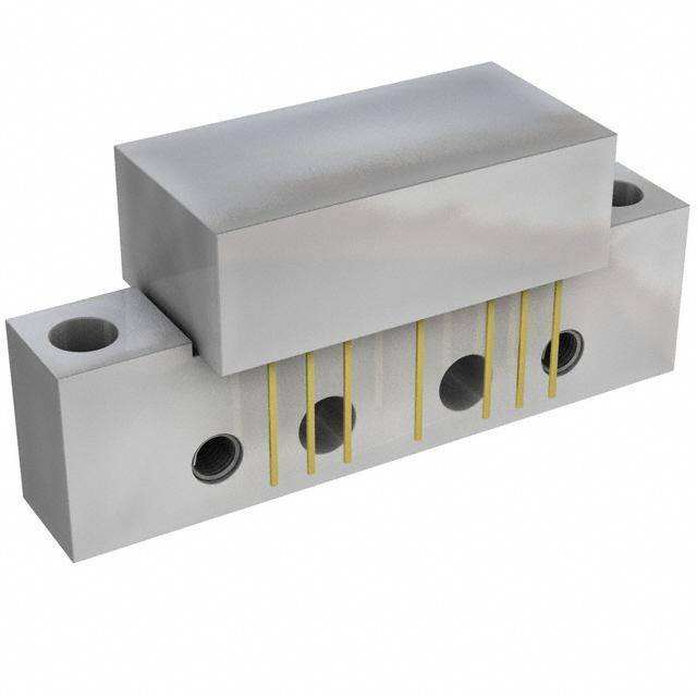
NXP Semiconductors Product specification 860 MHz, 20 dB gain power doubler BGD814 amplifier FEATURES PINNING - SOT115J Excellent linearity PIN DESCRIPTION Extremely low noise 1 input Excellent return loss properties 2,3 common Silicon nitride passivation 5 +V B Rugged construction 7,8 common Gold metallization ensures excellent reliability. 9 output APPLICATIONS CATV systems operating in the 40to870MHz handbook, halfpage 2 8 frequency range. 1 3 5 7 9 DESCRIPTION Side view MSA319 Hybrid amplifier module in a SOT115J package operating with a voltage supply of 24V(DC). Fig.1 Simplified outline. QUICK REFERENCE DATA SYMBOL PARAMETER CONDITIONS MIN. MAX. UNIT G power gain f=45MHz 19.7 20.3 dB p f=870MHz 20.5 21.5 dB I total current consumption(DC) V =24V 380 410 mA tot B LIMITING VALUES In accordance with the Absolute Maximum Rating System (IEC60134). SYMBOL PARAMETER MIN. MAX. UNIT V supply voltage 30 V B V RFinput voltage 70 dBmV i T storage temperature 40 +100 C stg T operating mounting base temperature 20 +100 C mb 2001Nov01 2
NXP Semiconductors Product specification 860 MHz, 20 dB gain power doubler BGD814 amplifier CHARACTERISTICS Bandwidth 40to870MHz; V =24V; T =35C; Z =Z =75. B mb S L SYMBOL PARAMETER CONDITIONS MIN. TYP. MAX. UNIT G power gain f=45MHz 19.7 20.3 dB p f=870MHz 20.5 21.5 dB SL slope straight line f=45to870MHz; note1 0.5 1.5 dB FL flatness straight line f=45to100MHz 0.25 dB f=100to800MHz 0.5 dB f=800to870MHz 0.4 0.1 dB s input return losses f=45to80MHz 25 dB 11 f=80to160MHz 22 dB f=160to320MHz 19 dB f=320to550MHz 17 dB f=550to650MHz 17 dB f=650to750MHz 16 dB f=750to870MHz 15 dB f=870to914MHz 12 dB s output return losses f=45to80MHz 24 dB 22 f=80to160MHz 22 dB f=160to320MHz 17 dB f=320to550MHz 18 dB f=550to650MHz 16 dB f=650to750MHz 15 dB f=750to870MHz 15 dB f=870to914MHz 13 dB s phase response f=50MHz 45 +45 deg 21 CTB composite triple beat 79chs flat; V =44dBmV; f =547.25MHz 66 dB o m 112chs flat; V =44dBmV; f =745.25MHz 60.5 dB o m 132chs flat; V =44dBmV; f =859.25MHz 56 dB o m 112chs; f =547.25MHz; V =50.2dBmV at 55.5 dB m o 745MHz; note2 79chs; f =331.25MHz; V =47.3dBmV at 65 dB m o 547MHz; note3 X cross modulation 79chs flat; V =44dBmV; f =55.25MHz 66 dB mod o m 112chs flat; V =44dBmV; f =55.25MHz 62.5 dB o m 132chs flat; V =44dBmV; f =55.25MHz 61 dB o m 112chs; f =745.25MHz; V =50.2dBmV at 57 dB m o 745MHz; note2 79chs; f =445.25MHz; V =47.3dBmV at 66 dB m o 547MHz; note3 2001Nov01 3
NXP Semiconductors Product specification 860 MHz, 20 dB gain power doubler BGD814 amplifier SYMBOL PARAMETER CONDITIONS MIN. TYP. MAX. UNIT CSO composite second 79chs flat; V =44dBmV; f =548.5MHz 68 dB o m order distortion 112chs flat; V =44dBmV; f =746.5MHz 61 dB o m 132chs flat; V =44dBmV; f =860.5MHz 57 dB o m 112chs; f =210MHz; V =50.2dBmV at 56 dB m o 745MHz; note2 79 chs; f =210MHz; V =47.3dBmV at 64 dB m o 547MHz; note3 d second order distortion note4 69 dB 2 V output voltage d =60dB; note5 64 dBmV o im CTB compression=1dB; 132chs flat; 48 dBmV f=859.25MHz CSO compression=1dB; 132chs flat; 50 dBmV f=860.5MHz NF noise figure f=50MHz 5.5 dB f=550MHz 5.5 dB f=750MHz 6.5 dB f=870MHz 7.5 dB I total current note6 380 395 410 mA tot consumption(DC) Notes 1. Slope straight line is defined as gain at870MHz against gain at 45MHz. 2. Tilt=10.2dB (55to745MHz). 3. Tilt=7.3dB (55to547MHz). 4. f =55.25MHz; V =44dBmV; f =805.25MHz; V =44dBmV; measured at f +f =860.5MHz. p p q q p q 5. Measured according to DIN45004B: f =851.25MHz; V =V ; f =858.25MHz; V =V 6dB; f =860.25MHz; p p o q q o r V =V 6dB; measured at f +f f =849.25MHz. r o p q r 6. The module normally operates at V =24V, but is able to withstand supply transients up to 35V. B 2001Nov01 4
NXP Semiconductors Product specification 860 MHz, 20 dB gain power doubler BGD814 amplifier MLD345 MLD346 −50 52 −40 52 handbook, halfpage handbook, halfpage CTB (1) Vo Xmod (1) Vo (dB) (dBmV) (dB) (dBmV) −60 48 −50 48 −70 44 −60 44 (2) (3) (2) (4) −80 (3) 40 −70 40 (4) −90 36 −80 36 0 200 400 600 800 1000 0 200 400 600 800 1000 f (MHz) f (MHz) ZS=ZL=75; VB=24V; 79chs; tilt=7.3dB (50to550MHz). ZS=ZL=75; VB=24V; 79chs; tilt=7.3dB (50to550MHz). (1) Vo. (3) Typ. (1) Vo. (3) Typ. (2) Typ.+3. (4) Typ.3. (2) Typ.+3. (4) Typ.3. Fig.2 Composite triple beat as a function of Fig.3 Cross modulation as a function of frequency frequency under tilted conditions. under tilted conditions. MLD347 −60 52 handbook, halfpage (1) CSO Vo (dB) (2) (dBmV) −70 48 −80 (3) 44 −90 40 (4) −100 36 0 200 400 600 800 1000 f (MHz) ZS=ZL=75; VB=24V; 79chs; tilt=7.3dB (50to550MHz). (1) Vo. (3) Typ. (2) Typ.+3. (4) Typ.3. Fig.4 Composite second order distortion as a function of frequency under tilted conditions. 2001Nov01 5
NXP Semiconductors Product specification 860 MHz, 20 dB gain power doubler BGD814 amplifier MLD348 MLD349 −40 52 −40 52 handbook, halfpage handbook, halfpage CTB (1) Vo Xmod (1) Vo (dB) (dBmV) (dB) (dBmV) −50 48 −50 48 (2) −60 (2) 44 −60 (3) 44 (3) (4) (4) −70 40 −70 40 −80 36 −80 36 0 200 400 600 800 1000 0 200 400 600 800 1000 f (MHz) f (MHz) ZS=ZL=75; VB=24V; 112chs; tilt=10.3dB (50to750MHz). ZS=ZL=75; VB=24V; 112chs; tilt=10.3dB (50to750MHz). (1) Vo. (3) Typ. (1) Vo. (3) Typ. (2) Typ.+3. (4) Typ.3. (2) Typ.+3. (4) Typ.3. Fig.5 Composite triple beat as a function of Fig.6 Cross modulation as a function of frequency frequency under tilted conditions. under tilted conditions. MLD350 −50 52 handbook, halfpage (1) CSO Vo (dB) (dBmV) −60 (2) 48 −70 (3) 44 −80 (4) 40 −90 36 0 200 400 600 800 1000 f (MHz) ZS=ZL=75; VB=24V; 112chs; tilt=10.3dB (50to750MHz). (1) Vo. (3) Typ. (2) Typ.+3. (4) Typ.3. Fig.7 Composite second order distortion as a function of frequency under tilted conditions. 2001Nov01 6
NXP Semiconductors Product specification 860 MHz, 20 dB gain power doubler BGD814 amplifier PACKAGE OUTLINE Rectangular single-ended package; aluminium flange; 2 vertical mounting holes; 2 x 6-32 UNC and 2 extra horizontal mounting holes; 7 gold-plated in-line leads SOT115J D E Z p A2 1 2 3 5 7 8 9 A L F S c W e b w M d e1 U2 Q q2 y M B B q1 x M B y M B p U1 q 0 5 10 mm scale DIMENSIONS (mm are the original dimensions) UNITmAax. mAa2x. b c mDax. d mEax. e e1 F mLin. p mQax. q q1 q2 S U1 U2 W w x y mZax. 0.51 2.04 4.15 44.75 8.2 6-32 mm 20.8 9.5 0.25 27.2 13.75 2.54 5.08 12.7 8.8 2.4 38.1 25.4 10.2 4.2 0.25 0.7 0.1 3.8 0.38 2.54 3.85 44.25 7.8 UNC OUTLINE REFERENCES EUROPEAN ISSUE DATE VERSION IEC JEDEC JEITA PROJECTION 04-02-04 SOT115J 10-06-18 2001Nov01 7
NXP Semiconductors Product specification 860 MHz, 20 dB gain power doubler BGD814 amplifier DATA SHEET STATUS DOCUMENT PRODUCT DEFINITION STATUS(1) STATUS(2) Objective data sheet Development This document contains data from the objective specification for product development. Preliminary data sheet Qualification This document contains data from the preliminary specification. Product data sheet Production This document contains the product specification. Notes 1. Please consult the most recently issued document before initiating or completing a design. 2. The product status of device(s) described in this document may have changed since this document was published and may differ in case of multiple devices. The latest product status information is available on the Internet at URLhttp://www.nxp.com. DISCLAIMERS property or environmental damage. NXP Semiconductors accepts no liability for inclusion and/or use of NXP Limited warranty and liability Information in this Semiconductors products in such equipment or document is believed to be accurate and reliable. applications and therefore such inclusion and/or use is at However, NXP Semiconductors does not give any the customer’s own risk. representations or warranties, expressed or implied, as to the accuracy or completeness of such information and Applications Applications that are described herein for shall have no liability for the consequences of use of such any of these products are for illustrative purposes only. information. NXP Semiconductors makes no representation or warranty that such applications will be suitable for the In no event shall NXP Semiconductors be liable for any specified use without further testing or modification. indirect, incidental, punitive, special or consequential damages (including - without limitation - lost profits, lost Customers are responsible for the design and operation of savings, business interruption, costs related to the their applications and products using NXP removal or replacement of any products or rework Semiconductors products, and NXP Semiconductors charges) whether or not such damages are based on tort accepts no liability for any assistance with applications or (including negligence), warranty, breach of contract or any customer product design. It is customer’s sole other legal theory. responsibility to determine whether the NXP Semiconductors product is suitable and fit for the Notwithstanding any damages that customer might incur customer’s applications and products planned, as well as for any reason whatsoever, NXP Semiconductors’ for the planned application and use of customer’s third aggregate and cumulative liability towards customer for party customer(s). Customers should provide appropriate the products described herein shall be limited in design and operating safeguards to minimize the risks accordance with the Terms and conditions of commercial associated with their applications and products. sale of NXP Semiconductors. NXP Semiconductors does not accept any liability related Right to make changes NXP Semiconductors to any default, damage, costs or problem which is based reserves the right to make changes to information on any weakness or default in the customer’s applications published in this document, including without limitation or products, or the application or use by customer’s third specifications and product descriptions, at any time and party customer(s). Customer is responsible for doing all without notice. This document supersedes and replaces all necessary testing for the customer’s applications and information supplied prior to the publication hereof. products using NXP Semiconductors products in order to Suitability for use NXP Semiconductors products are avoid a default of the applications and the products or of not designed, authorized or warranted to be suitable for the application or use by customer’s third party use in life support, life-critical or safety-critical systems or customer(s). NXP does not accept any liability in this equipment, nor in applications where failure or malfunction respect. of an NXP Semiconductors product can reasonably be expected to result in personal injury, death or severe 2001Nov01 8
NXP Semiconductors Product specification 860 MHz, 20 dB gain power doubler BGD814 amplifier Limiting values Stress above one or more limiting Quick reference data The Quick reference data is an values (as defined in the Absolute Maximum Ratings extract of the product data given in the Limiting values and System of IEC60134) will cause permanent damage to Characteristics sections of this document, and as such is the device. Limiting values are stress ratings only and not complete, exhaustive or legally binding. (proper) operation of the device at these or any other Non-automotive qualified products Unless this data conditions above those given in the Recommended sheet expressly states that this specific NXP operating conditions section (if present) or the Semiconductors product is automotive qualified, the Characteristics sections of this document is not warranted. product is not suitable for automotive use. It is neither Constant or repeated exposure to limiting values will qualified nor tested in accordance with automotive testing permanently and irreversibly affect the quality and or application requirements. NXP Semiconductors accepts reliability of the device. no liability for inclusion and/or use of non-automotive Terms and conditions of commercial sale NXP qualified products in automotive equipment or Semiconductors products are sold subject to the general applications. terms and conditions of commercial sale, as published at In the event that customer uses the product for design-in http://www.nxp.com/profile/terms, unless otherwise and use in automotive applications to automotive agreed in a valid written individual agreement. In case an specifications and standards, customer (a) shall use the individual agreement is concluded only the terms and product without NXP Semiconductors’ warranty of the conditions of the respective agreement shall apply. NXP product for such automotive applications, use and Semiconductors hereby expressly objects to applying the specifications, and (b) whenever customer uses the customer’s general terms and conditions with regard to the product for automotive applications beyond NXP purchase of NXP Semiconductors products by customer. Semiconductors’ specifications such use shall be solely at No offer to sell or license Nothing in this document customer’s own risk, and (c) customer fully indemnifies may be interpreted or construed as an offer to sell products NXP Semiconductors for any liability, damages or failed that is open for acceptance or the grant, conveyance or product claims resulting from customer design and use of implication of any license under any copyrights, patents or the product for automotive applications beyond NXP other industrial or intellectual property rights. Semiconductors’ standard warranty and NXP Semiconductors’ product specifications. Export control This document as well as the item(s) described herein may be subject to export control regulations. Export might require a prior authorization from national authorities. 2001Nov01 9
NXP Semiconductors provides High Performance Mixed Signal and Standard Product solutions that leverage its leading RF, Analog, Power Management, Interface, Security and Digital Processing expertise Customer notification This data sheet was changed to reflect the new company name NXP Semiconductors, including new legal definitions and disclaimers. No changes were made to the technical content, except for package outline drawings which were updated to the latest version. Contact information For additional information please visit: http://www.nxp.com For sales offices addresses send e-mail to: salesaddresses@nxp.com © NXP B.V. 2010 All rights are reserved. Reproduction in whole or in part is prohibited without the prior written consent of the copyright owner. The information presented in this document does not form part of any quotation or contract, is believed to be accurate and reliable and may be changed without notice. No liability will be accepted by the publisher for any consequence of its use. Publication thereof does not convey nor imply any license under patent- or other industrial or intellectual property rights. Printed in The Netherlands 613518/04/pp10 Date of release: 2001Nov01 Document order number: 939775008857