ICGOO在线商城 > 集成电路(IC) > 线性 - 放大器 - 视频放大器和频缓冲器 > AD828AR
 Datasheet下载
- 型号: AD828AR
- 制造商: Analog
- 库位|库存: xxxx|xxxx
- 要求:
| 数量阶梯 | 香港交货 | 国内含税 |
| +xxxx | $xxxx | ¥xxxx |
查看当月历史价格
查看今年历史价格
AD828AR产品简介:
ICGOO电子元器件商城为您提供AD828AR由Analog设计生产,在icgoo商城现货销售,并且可以通过原厂、代理商等渠道进行代购。 AD828AR价格参考¥46.30-¥52.09。AnalogAD828AR封装/规格:线性 - 放大器 - 视频放大器和频缓冲器, Video Amp, 2 Voltage Feedback 8-SOIC。您可以下载AD828AR参考资料、Datasheet数据手册功能说明书,资料中有AD828AR 详细功能的应用电路图电压和使用方法及教程。
AD828AR 是 Analog Devices Inc. 生产的一款高性能视频放大器,属于线性 - 放大器 - 视频放大器和缓冲器类别。它专为高速、低失真应用设计,具有宽广的带宽和卓越的动态性能,适用于多种场景。以下是 AD828AR 的主要应用场景:

 1. 视频信号处理
   - 视频放大:AD828AR 可用于视频信号的放大和驱动,支持复合视频、S-Video 和分量视频信号。其高带宽(300 MHz)确保了高质量的视频传输,适合高清或专业视频设备。
   - 视频缓冲:作为缓冲器使用时,AD828AR 能够降低输入阻抗对信号源的影响,同时保持信号完整性。

 2. 通信系统
   - 高速数据传输:AD828AR 的高增益带宽积(300 MHz)使其适用于高速数据通信系统,例如光纤通信中的信号调理。
   - 射频前端:在某些低频率的射频应用中,AD828AR 可用作信号调理放大器,提供低失真的信号增益。

 3. 医疗设备
   - 超声波成像:AD828AR 的低噪声特性和高精度使其成为超声波接收链路中信号放大的理想选择。
   - 心电图 (ECG) 和脑电图 (EEG):在需要高速信号处理的医疗设备中,AD828AR 可以用于前置放大器,以提高信号质量。

 4. 工业自动化
   - 传感器信号放大:在工业控制领域,AD828AR 可用于放大来自传感器的微弱信号,例如压力、温度或位移传感器。
   - 数据采集系统:其快速响应和低失真特性使其非常适合用于高速数据采集系统中的信号调理。

 5. 测试与测量
   - 示波器和信号发生器:AD828AR 的高带宽和低失真特性使其成为测试与测量设备的理想选择,能够准确再现复杂波形。
   - 信号调理模块:在各种测试仪器中,AD828AR 可用于信号的放大、滤波和缓冲。

 6. 消费电子产品
   - 家庭影院系统:AD828AR 可用于音频/视频信号的处理和放大,提升画质和音质表现。
   - 游戏设备:在需要高速信号处理的游戏控制器或显示设备中,AD828AR 提供可靠的性能支持。

 总结
AD828AR 凭借其高带宽、低失真和低噪声的特点,在视频信号处理、通信系统、医疗设备、工业自动化、测试与测量以及消费电子等多个领域都有广泛应用。它是一款多功能、高性能的视频放大器,能够满足各种高速信号处理需求。
| 参数 | 数值 |
| -3db带宽 | 130MHz |
| 产品目录 | 集成电路 (IC)半导体 |
| 描述 | IC VIDEO OPAMP DUAL LP 8-SOIC视频放大器 IC Dual Low Power |
| 产品分类 | |
| 品牌 | Analog Devices Inc |
| 产品手册 | |
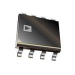
| 产品图片 |
|
| rohs | 否不符合限制有害物质指令(RoHS)规范要求 |
| 产品系列 | 放大器 IC,视频放大器,Analog Devices AD828AR- |
| 数据手册 | |
| 产品型号 | AD828AR |
| PCN过时产品 | |
| 产品种类 | 视频放大器 |
| 供应商器件封装 | 8-SOIC |
| 包装 | 管件 |
| 压摆率 | 450 V/µs |
| 双重电源电压 | +/- 2.5 V to +/- 18 V |
| 商标 | Analog Devices |
| 增益带宽生成 | 45 MHz |
| 安装类型 | 表面贴装 |
| 安装风格 | SMD/SMT |
| 封装 | Tube |
| 封装/外壳 | 8-SOIC(0.154",3.90mm 宽) |
| 封装/箱体 | SOIC-8 |
| 工作温度范围 | - 40 C to + 85 C |
| 工作电源电压 | 5 V to 36 V |
| 工厂包装数量 | 98 |
| 带宽 | 130 MHz |
| 应用 | 电压反馈 |
| 放大器类型 | Voltage Feedback Amplifier |
| 最大双重电源电压 | +/- 18 V |
| 最大工作温度 | + 85 C |
| 最小双重电源电压 | +/- 2.5 V |
| 最小工作温度 | - 40 C |
| 标准包装 | 98 |
| 电压-电源,单/双 (±) | 5 V ~ 36 V, ±2.5 V ~ 18 V |
| 电流-电源 | 14mA |
| 电流-输出/通道 | 50mA |
| 电源电压-最大 | 36 V |
| 电源电压-最小 | 5 V |
| 电源电流 | 14 mA |
| 电源类型 | Dual |
| 电路数 | 2 |
| 系列 | AD828 |
| 输出类型 | - |
| 通道数量 | 2 Channel |


- 商务部:美国ITC正式对集成电路等产品启动337调查
- 曝三星4nm工艺存在良率问题 高通将骁龙8 Gen1或转产台积电
- 太阳诱电将投资9.5亿元在常州建新厂生产MLCC 预计2023年完工
- 英特尔发布欧洲新工厂建设计划 深化IDM 2.0 战略
- 台积电先进制程称霸业界 有大客户加持明年业绩稳了
- 达到5530亿美元!SIA预计今年全球半导体销售额将创下新高
- 英特尔拟将自动驾驶子公司Mobileye上市 估值或超500亿美元
- 三星加码芯片和SET,合并消费电子和移动部门,撤换高东真等 CEO
- 三星电子宣布重大人事变动 还合并消费电子和移动部门
- 海关总署:前11个月进口集成电路产品价值2.52万亿元 增长14.8%


PDF Datasheet 数据手册内容提取
a Dual, Low Power Video Op Amp AD828 FEATURES FUNCTIONAL BLOCK DIAGRAM Excellent Video Performance Differential Gain and Phase Error of 0.01% and 0.05(cid:1) High Speed OUT1 1 8 V+ 130 MHz 3 dB Bandwidth (G = +2) 450 V/(cid:2)s Slew Rate –IN1 2 7 OUT2 80 ns Settling Time to 0.01% +IN1 3 6 –IN2 Low Power 15 mA Max Power Supply Current V– 4 5 +IN2 AD828 High Output Drive Capability 50 mA Minimum Output Current per Amplifier Ideal for Driving Back Terminated Cables Flexible Power Supply Specified for +5 V, (cid:3)5 V, and (cid:3)15 V Operation (cid:3)3.2 V Min Output Swing into a 150 (cid:4) Load (V = (cid:3)5 V) S Excellent DC Performance 2.0 mV Input Offset Voltage Available in 8-Lead SOIC and 8-Lead Plastic Mini-DIP GENERAL DESCRIPTION The AD828 is fully specified for operation with a single 5 V The AD828 is a low cost, dual video op amp optimized for use power supply and with dual supplies from ±5 V to ±15 V. This in video applications that require gains of +2 or greater and power supply flexibility, coupled with a very low supply current high output drive capability, such as cable driving. Due to its of 15 mA and excellent ac characteristics under all power supply low power and single-supply functionality, along with excellent conditions, make the AD828 the ideal choice for many demand- differential gain and phase errors, the AD828 is ideal for power- ing yet power-sensitive applications. sensitive applications such as video cameras and professional The AD828 is a voltage feedback op amp that excels as a gain video equipment. stage (gains > +2) or active filter in high speed and video systems With video specs like 0.1 dB flatness to 40 MHz and low and achieves a settling time of 45 ns to 0.1%, with a low input differential gain and phase errors of 0.01% and 0.05°, along offset voltage of 2 mV max. with 50 mA of output current per amplifier, the AD828 is an The AD828 is available in low cost, small 8-lead plastic mini-DIP excellent choice for any video application. The 130 MHz gain and SOIC packages. bandwidth and 450 V/µs slew rate make the AD828 useful in many high speed applications, including video monitors, CATV, color copiers, image scanners, and fax machines. 0.03ent c er P +V 0.1(cid:2)F 0.02 N – AI DIFF GAIN G VIN R75T(cid:4) AD1/8228 R75B(cid:4)T 75(cid:4) Degrees 0.07 0.01 RENTIAL 0.1(cid:2)F R75T(cid:4) ASE – 0.06 DIFFE H P –V L DIFF PHASE 1k(cid:4) 1k(cid:4) NTIA 0.05 E R E F F Figure 1.Video Line Driver DI 0.04 5 10 15 SUPPLY VOLTAGE – (cid:3)V Figure 2.Differential Phase vs. Supply Voltage REV.C Information furnished by Analog Devices is believed to be accurate and reliable. However, no responsibility is assumed by Analog Devices for its use, nor for any infringements of patents or other rights of third parties that One Technology Way, P.O. Box 9106, Norwood, MA 02062-9106, U.S.A. may result from its use. No license is granted by implication or otherwise Tel: 781/329-4700www.analog.com under any patent or patent rights of Analog Devices. Fax: 781/326-8703 © Analog Devices, Inc., 2002
AD828–SPECIFICATIONS (@ T = 25(cid:1)C, unless otherwise noted.) A Parameter Conditions V Min Typ Max Unit S DYNAMIC PERFORMANCE –3 dB Bandwidth Gain = +2 ±5 V 60 85 MHz ±15 V 100 130 MHz 0, +5 V 30 45 MHz Gain = –1 ±5 V 35 55 MHz ±15 V 60 90 MHz 0, +5 V 20 35 MHz Bandwidth for 0.1 dB Flatness Gain = +2 ±5 V 30 43 MHz C = 1 pF ±15 V 30 40 MHz C 0, +5 V 10 18 MHz Gain = –1 ±5 V 15 25 MHz C = 1 pF ±15 V 30 50 MHz C 0, +5 V 10 19 MHz Full Power Bandwidth* V = 5 V p-p OUT R = 500 Ω ±5 V 22.3 MHz LOAD V = 20 V p-p OUT R = 1 kΩ ±15 V 7.2 MHz LOAD Slew Rate R = 1 kΩ ±5 V 300 350 V/µs LOAD Gain = –1 ±15 V 400 450 V/µs 0, +5 V 200 250 V/µs Settling Time to 0.1% –2.5 V to +2.5 V ±5 V 45 ns 0 V–10 V Step, A = –1 ±15 V 45 ns V Settling Time to 0.01% –2.5 V to +2.5 V ±5 V 80 ns 0 V–10 V Step, A = –1 ±15 V 80 ns V NOISE/HARMONIC PERFORMANCE Total Harmonic Distortion F = 1 MHz ±15 V –78 dB C Input Voltage Noise f = 10 kHz ±5 V, ±15 V 10 nV/√Hz Input Current Noise f = 10 kHz ±5 V, ±15 V 1.5 pA/√Hz Differential Gain Error NTSC ±15 V 0.01 0.02 % (R = 150 Ω) Gain = +2 ±5 V 0.02 0.03 % L 0, +5 V 0.08 % Differential Phase Error NTSC ±15 V 0.05 0.09 Degrees (R = 150 Ω) Gain = +2 ±5 V 0.07 0.1 Degrees L 0, +5 V 0.1 Degrees DC PERFORMANCE Input Offset Voltage ±5 V, ±15 V 0.5 2 mV T to T 3 mV MIN MAX Offset Drift 10 µV/°C Input Bias Current ±5 V, ±15 V 3.3 6.6 µA T 10 µA MIN T 4.4 µA MAX Input Offset Current ±5 V, ±15 V 25 300 nA T to T 500 nA MIN MAX Offset Current Drift 0.3 nA/°C Open-Loop Gain V = ±2.5 V ±5 V OUT R = 500 Ω 3 5 V/mV LOAD T to T 2 V/mV MIN MAX R = 150 Ω 2 4 V/mV LOAD V = ±10 V ±15 V OUT R = 1 kΩ 5.5 9 V/mV LOAD T to T 2.5 V/mV MIN MAX V = ±7.5 V ±15 V OUT R = 150 Ω (50 mA Output) 3 5 V/mV LOAD INPUT CHARACTERISTICS Input Resistance 300 kΩ Input Capacitance 1.5 pF Input Common-Mode Voltage Range ±5 V +3.8 +4.3 V –2.7 –3.4 V ±15 V +13 +14.3 V –12 –13.4 V 0, +5 V +3.8 +4.3 V +1.2 +0.9 V Common-Mode Rejection Ratio V = +2.5 V, T to T ±5 V 82 100 dB CM MIN MAX V = ±12 V ±15 V 86 120 dB CM T to T ±15 V 84 100 dB MIN MAX –2– REV. C
AD828 Parameter Conditions V Min Typ Max Unit S OUTPUT CHARACTERISTICS Output Voltage Swing R = 500 Ω ±5 V 3.3 3.8 ±V LOAD R = 150 Ω ±5 V 3.2 3.6 ±V LOAD R = 1 kΩ ±15 V 13.3 13.7 ±V LOAD R = 500 Ω ±15 V 12.8 13.4 ±V LOAD 1.5 R = 500 Ω 0, +5 V 3.5 ±V LOAD Output Current ±15 V 50 mA ±5 V 40 mA 0, +5 V 30 mA Short Circuit Current ±15 V 90 mA Output Resistance Open-Loop 8 Ω MATCHING CHARACTERISTICS Dynamic Crosstalk f = 5 MHz ±15 V –80 dB Gain Flatness Match G = +1, f = 40 MHz ±15 V 0.2 dB Skew Rate Match G = –1 ±15 V 10 V/µs DC Input Offset Voltage Match T to T ±5 V, ±15 V 0.5 2 mV MIN MAX Input Bias Current Match T to T ±5 V, ±15 V 0.06 0.8 µA MIN MAX Open-Loop Gain Match V = ±10 V, R = 1 kΩ, T to T ±15 V 0.01 0.15 mV/V O L MIN MAX Common-Mode Rejection Ratio Match V = ±12 V, T to T ±15 V 80 100 dB CM MIN MAX Power Supply Rejection Ratio Match ±5 V to ±15 V, T to T 80 100 dB MIN MAX POWER SUPPLY Operating Range Dual Supply ±2.5 ±18 V Single Supply +5 +36 V Quiescent Current ±5 V 14.0 15 mA T to T ±5 V 14.0 15 mA MIN MAX T to T ±5 V 15 mA MIN MAX Power Supply Rejection Ratio V = ±5 V to ±15 V, T to T 80 90 dB S MIN MAX *Full power bandwidth = slew rate/2 π VPEAK. ORDERING GUIDE Specifications subject to change without notice. Temperature Package Package Model Range Description Option ABSOLUTE MAXIMUM RATINGS1 AD828AN –40°C to +85°C 8-Lead Plastic DIP N-8 Supply Voltage . . . . . . . . . . . . . . . . . . . . . . . . . . . . . . . . ±18 V AD828AR –40°C to +85°C 8-Lead Plastic SOIC SO-8 Internal Power Dissipation2 AD828AR-REEL7–40°C to +85°C 7" Tape and Reel SO-8 Plastic DIP (N) . . . . . . . . . . . . . . . . . . See Derating Curves AD828AR-REEL –40°C to +85°C 13" Tape and Reel SO-8 Small Outline (R) . . . . . . . . . . . . . . . . . See Derating Curves 2.0 Input Voltage (Common Mode) . . . . . . . . . . . . . . . . . . . . ±VS TJ = 150(cid:1)C Differential Input Voltage . . . . . . . . . . . . . . . . . . . . . . . . ±6 V atts 8-LEAD MINI-DIP PACKAGE Output Short Circuit Duration . . . . . . . . See Derating Curves W Storage Temperature Range (N, R) . . . . . . . .–65°C to +125°C N – 1.5 O Operating Temperature Range . . . . . . . . . . . .–40°C to +85°C TI A Lead Temperature Range (Soldering 10 sec) . . . . . . . . +300°C SIP NOTES R DIS 1.0 1Stresses above those listed under Absolute Maximum Ratings may cause perma- WE nent damage to the device. This is a stress rating only; functional operation of the O P device at these or any other conditions above those indicated in the operational UM 0.5 section of this specification is not implied. Exposure to absolute maximum rating M conditions for extended periods may affect device reliability. AXI 8-LEAD SOIC PACKAGE 2Specification is for device in free air: M 8-Lead Plastic DIP Package: θJA = 100°C/W 0 8-Lead SOIC Package: θJA = 155°C/W –50–40–30–20–10 0 10 20 30 40 50 60 70 80 90 AMBIENT TEMPERATURE – (cid:1)C Figure 3.Maximum Power Dissipation vs. Temperature for Different Package Types CAUTION ESD (electrostatic discharge) sensitive device. Electrostatic charges as high as 4000V readily WARNING! accumulate on the human body and test equipment and can discharge without detection. Although the AD828 features proprietary ESD protection circuitry, permanent damage may occur on devices subjected to high energy electrostatic discharges. Therefore, proper ESD precautions are recommended to avoid performance degradation or loss of functionality. ESD SENSITIVE DEVICE REV. C –3–
AD828—Typical Performance Characteristics 20 7.7 A m – V P (cid:3) M – A E 15 R 7.2 G E N P ON-MODE RA 10 +–VVCCMM LY CURRENT 6.7 –+4805(cid:1)(cid:1)CC +25(cid:1)C M P INPUT COM 5 ESCENT SUP 6.2 UI Q 0 5.7 0 5 10 15 20 0 5 10 15 20 SUPPLY VOLTAGE – (cid:3)V SUPPLY VOLTAGE – (cid:3)V TPC 1.Common-Mode Voltage Range vs. Supply TPC 4.Quiescent Supply Current per Amp vs. Supply Voltage Voltage for Various Temperatures 20 500 V (cid:3) – 15 450 NG (cid:2)s WI V/ E S RL = 500(cid:4) E – AG10 AT 400 T R UT VOL RL = 150(cid:4) SLEW P T 5 350 U O 0 300 0 5 10 15 20 0 5 10 15 20 SUPPLY VOLTAGE – (cid:3)V SUPPLY VOLTAGE – (cid:3)V TPC 2.Output Voltage Swing vs. Supply Voltage TPC 5.Slew Rate vs. Supply Voltage 30 100 (cid:4) NG – V p-p 2205 Vs = (cid:3)15V PEDANCE – 10 WI M E S UT I AG 15 TP 1 T U L O T VO 10 OOP UTPU Vs = (cid:3)5V ED-L 0.1 O 5 OS L C 0 0.01 10 100 1k 10k 1k 10k 100k 1M 10M 100M LOAD RESISTANCE – (cid:4) FREQUENCY – Hz TPC 3.Output Voltage Swing vs. Load Resistance TPC 6.Closed-Loop Output Impedance vs. Frequency –4– REV. C
AD828 7 100 100 PHASE (cid:3)5V OR (cid:3)15V SUPPLIES 6 80 80 s (cid:2)PUT BIAS CURRENT – A 435 OPEN-LOOP GAIN – dB 426000 (cid:3)5V S(cid:3)U1P5PVL ISEUSPPLIES 426000 PHASE MARGIN – Degree N I 2 0 0 RL = 1k(cid:4) 1 –20 –60 –40 –20 0 20 40 60 80 100 120 140 1k 10k 100k 1M 10M 100M 1G TEMPERATURE – (cid:1)C FREQUENCY – Hz TPC 7.Input Bias Current vs. Temperature TPC 10.Open-Loop Gain and Phase Margin vs. Frequency 130 9 (cid:3)15V 8 mA110 NT – SOURCE CURRENT V/mV 7 URRE 90 AIN – (cid:3)5V T C SINK CURRENT P G 6 UI O RC 70 LO CI N- 5 ORT OPE SH 50 4 30 3 –60 –40 –20 0 20 40 60 80 100 120 140 100 1k 10k TEMPERATURE – (cid:1)C LOAD RESISTANCE – (cid:4) TPC 8.Short Circuit Current vs. Temperature TPC 11.Open-Loop Gain vs. Load Resistance 80 80 100 90 80 ees 70 PHASE MARGIN 70Hz +SUPPLY GIN – Degr 60 60WIDTH – M R – dB 6700 AR ND SR 50 ASE M GAIN BANDWIDTH dB BA P 40 –SUPPLY PH 50 50–3 30 20 40 40 10 –60 –40 –20 0 20 40 60 80 100 120 140 100 1k 10k 100k 1M 10M 100M TEMPERATURE – (cid:1)C FREQUENCY – Hz TPC 9.–3 dB Bandwidth and Phase Margin vs. TPC 12.Power Supply Rejection vs. Frequency Temperature, Gain = +2 REV. C –5–
AD828 140 –40 VIN = 1V p-p GAIN = +2 –50 B 120 – d N –60 O TI B R d O CMR – 100 C DIST –70 NI O –80 RM 2ND HARMONIC 80 A H –90 3RD HARMONIC 60 –100 1k 10k 100k 1M 10M 100 1k 10k 100k 1M 10M FREQUENCY – Hz FREQUENCY – Hz TPC 13.Common-Mode Rejection vs. Frequency TPC 16.Harmonic Distortion vs. Frequency 30 50 Hz 40 p RL = 1k(cid:4) V/ TAGE – V p- 20 E NOISE – n 30 L G VO TA 20 UT 10 RL = 150(cid:4) OL P V UT UT O P 10 N I 0 0 100k 1M 10M 100M 0 10 100 1k 10k 100k 1M 10M FREQUENCY – Hz FREQUENCY – Hz TPC 14.Large Signal Frequency Response TPC 17.Input Voltage Noise Spectral Density vs. Frequency 10 650 8 V 6 (cid:3) O 550 T 4 FROM 0 2 1% 0.1% 0.01% (cid:2)E – V/s G 0 AT 450 N R WI(cid:5)2 W S 1% 0.1% 0.01% E UT (cid:5)4 SL P T 350 OU(cid:5)6 (cid:5)8 (cid:5)10 250 0 20 40 60 80 100 120 140 160 –60 –40 –20 0 20 40 60 80 100 120 140 SETTLING TIME (cid:5) ns TEMPERATURE – (cid:1)C TPC 15.Output Swing and Error vs. Settling Time TPC 18.Slew Rate vs. Temperature –6– REV. C
AD828 10 5 8 1pF 0.1dB 4 1pF 0.1dB 46 1k(cid:4) AD18k2(cid:4)8 VOUT +V(cid:3)(cid:3)5S15V5VVF441038LMMMATHHHNzzzESS 23 VIN1k(cid:4) AD18k2(cid:4)8 VOUT V(cid:3)(cid:3)+5S15V5VVF521059LMMMATHHHNzzzESS B 2 VIN 150(cid:4) VS = (cid:3)15V B 1 150(cid:4) VS = (cid:3)15V d d N – 0 N – 0 AI AI G –2 G –1 VS = +5V –4 VS = (cid:3)5V –2 VS = (cid:3)5V –6 –3 VS = +5V –8 –4 –10 –5 100k 1M 10M 100M 100k 1M 10M 100M FREQUENCY – Hz FREQUENCY – Hz TPC 19.Closed-Loop Gain vs. Frequency TPC 22.Closed-Loop Gain vs. Frequency, G = –1 0.03nt 1.0 e c er 0.8 P 0.02N – 0.6 AI G DIFF GAIN L 0.4 A Degrees0.07 0.01FERENTI N – dB 0.20 VS = (cid:3)15V E – 0.06 DIF GAI –0.2 PHAS –0.4 VS = (cid:3)5V L DIFF PHASE NTIA0.05 –0.6 VS = (cid:6)5V RE –0.8 E F DIF0.045 10 15 –1.0100k 1M 10M 100M SUPPLY VOLTAGE – (cid:3)V FREQUENCY – Hz TPC 20.Differential Gain and Phase vs. Supply Voltage TPC 23.Gain Flatness Matching vs. Supply, G = +2 –30 (cid:6)5V –40 0.1(cid:2)F –50 1(cid:2)F VOUT LK – dB –60 VIN 3AD1/82288 1 7 AD1/8228 5 TA –70 RL = 150(cid:4) 2 4 6 S S RO –80 C 0.1(cid:2)F –90 RL = 1k(cid:4) RL RL 1(cid:2)F –100 (cid:5)5V –110 10k 100k 1M 10M 100M USE GROUND PLANE FREQUENCY – Hz PINOUT SHOWN IS FOR MINI-DIP PACKAGE TPC 21.Crosstalk vs. Frequency TPC 24.Crosstalk Test Circuit REV. C –7–
AD828 CF 5V 50ns 1k(cid:4) 100 +VS 3.3(cid:2)F 90 0.01(cid:2)F HP PULSE (LS) VIN 1k(cid:4) OR FUNCTION (SS) 2 8 GENERATOR 1/2 VOUT TEKTRONIX TEKTRONIX 50(cid:4) AD828 1 P6201 FET 7A24 3 4 0.01(cid:2)F PROBE PREAMP 10 0% RL 5V 3.3(cid:2)F –VS TPC 25.Inverting Amplifier Connection TPC 28.Inverter Large Signal Pulse Response (cid:3)15 V, S C = 1 pF, R = 1 kΩ F L 2V 50ns 200mV 10ns 100 100 90 90 10 10 0% 0% 2V 200mV TPC 26.Inverter Large Signal Pulse Response (cid:3)5 V, TPC 29.Inverter Small Signal Pulse Response (cid:3)15 V, S S CF = 1 pF, RL = 1 kΩ CF = 1 pF, RL = 1500 Ω 200mV 10ns 200mV 10ns 100 100 90 90 10 10 0% 0% 200mV 200mV TPC 27.Inverter Small Signal Pulse Response (cid:3)5 V, TPC 30.Inverter Small Signal Pulse Response (cid:3)5 V, S S C = 1 pF, R = 150 Ω C = 0 pF, R = 150 Ω F L F L –8– REV. C
AD828 CF 5V 50ns 1k(cid:4) 1k(cid:4) 100 +VS 3.3(cid:2)F 90 0.01(cid:2)F 2 8 1/2 VOUT TEKTRONIX TEKTRONIX HOGPRE N PFEUURLNASCTETO I(OLRNS) (SS) VIN R10IN0(cid:4) 3AD8248 01.01(cid:2)F PP6R2O0B1E FET 7PAR2E4AMP 100% 50(cid:4) RL 3.3(cid:2)F 5V –VS TPC 31. Noninverting Amplifier Connection TPC 34. Noninverting Large Signal Pulse Response (cid:3)15 V, C = 1 pF, R = 1 kΩ S F L 1V 50ns 100mV 10ns 100 100 90 90 10 10 0% 0% 2V 200mV TPC 32.Noninverting Large Signal Pulse Response TPC 35. Noninverting Small Signal Pulse Response (cid:3)5 VS, CF = 1 pF, RL = 1 kΩ (cid:3)15 V, C = 1 pF, R = 150 Ω S F L 100mV 10ns 100mV 10ns 100 100 90 90 10 10 0% 0% 200mV 200mV TPC 33. Noninverting Small Signal Pulse Response TPC 36. Noninverting Small Signal Pulse Response (cid:3)5 VS, CF = 1 pF, RL = 150 Ω (cid:3)5 V, C = 0 pF, R = 150 Ω S F L REV. C –9–
AD828 THEORY OF OPERATION Circuit Board Layout The AD828 is a low cost, dual video operational amplifier Input and output runs should be laid out so as to physically designed to excel in high performance, high output current isolate them from remaining runs. In addition, the feedback video applications. resistor of each amplifier should be placed away from the feed- back resistor of the other amplifier, since this greatly reduces The AD828 consists of a degenerated NPN differential pair interamp coupling. driving matched PNPs in a folded-cascade gain stage (Figure 4). The output buffer stage employs emitter followers in a class AB Choosing Feedback and Gain Resistors amplifier that delivers the necessary current to the load while To prevent the stray capacitance present at each amplifier’s maintaining low levels of distortion. summing junction from limiting its performance, the feedback resistors should be ≤ 1 kΩ. Since the summing junction capaci- The AD828 will drive terminated cables and capacitive loads of tance may cause peaking, a small capacitor (1 pF to 5 pF) may 10 pF or less. As the closed-loop gain is increased, the AD828 be paralleled with R to neutralize this effect. Finally, sockets will drive heavier cap loads without oscillating. F should be avoided, because of their tendency to increase interlead +VS capacitance. Power Supply Bypassing Proper power supply decoupling is critical to preserve the integrity of high frequency signals. In carefully laid out designs, decoupling capacitors should be placed in close proximity to the supply pins, while their lead lengths should be kept to a OUTPUT minimum. These measures greatly reduce undesired inductive –IN effects on the amplifier’s response. Though two 0.1 µF capacitors will typically be effective in decoupling the supplies, several capacitors of different values +IN can be paralleled to cover a wider frequency range. PARALLEL AMPS PROVIDE 100 mA TO LOAD –VS By taking advantage of the superior matching characteristics of the AD828, enhanced performance can easily be achieved by employ- Figure 4.Simplified Schematic ing the circuit in Figure 5. Here, two identical cells are paralleled to obtain even higher load driving capability than that of a single INPUT CONSIDERATIONS An input protection resistor (R in TPC 31) is required in circuits amplifier (100 mA min guaranteed). R1 and R2 are included to IN where the input to the AD828 will be subjected to transient or limit current flow between amplifier outputs that would arise in continuous overload voltages exceeding the ±6 V maximum dif- the presence of any residual mismatch. ferential limit. This resistor provides protection for the input transistors by limiting their maximum base current. 1k(cid:4) +VS 1(cid:2)F For high performance circuits, the “balancing” resistor should be 0.1(cid:2)F used to reduce the offset errors caused by bias current flowing tehqruoaulsg hth teh ep ainrapluletl acnodm fbeiendabtiaocnk oref sRisto rasn. dT Rhe abnadla nthcuinsg p rreosviisdtoers 1k(cid:4) 2 1/28 5R(cid:4)1 IN F 1 AD828 a matched impedance at each input terminal. The offset voltage 3 error will then be reduced by more than an order of magnitude. VIN VOUT APPLYING THE AD828 The AD828 is a breakthrough dual amp that delivers precision and 5 1/2 5R(cid:4)2 RL speed at low cost with low power consumption. The AD828 offers 1k(cid:4) AD828 7 excellent static and dynamic matching characteristics, combined 6 4 0.1(cid:2)F with the ability to drive heavy resistive loads. 1(cid:2)F As with all high frequency circuits, care should be taken to main- tain overall device performance as well as their matching. The 1k(cid:4) –VS following items are presented as general design considerations. Figure 5.Parallel Amp Configuration –10– REV. C
AD828 AIN 510(cid:4) 3 1/2 1 RZ RZ 1 1/2 3 510(cid:4)BIN AD828 AD828 2 2 510(cid:4) 100FT 510(cid:4) RG59A/U 510(cid:4) RZ = 75(cid:4) 510(cid:4) 536(cid:4) 536(cid:4) 6 6 1/2 1/2 BOUT 7 AD828 AD828 7 AOUT 5 5 Figure 6.Bidirectional Transmission CKT Full-Duplex Transmission clearly show that each input signal appears undisturbed at its out- Superior load handling capability (50 mA min/amp), high put, while the unwanted signal is eliminated at either receiver. bandwidth, wide supply voltage range, and excellent crosstalk The transmitters operate as followers, while the receivers’ gain rejection makes the AD828 an ideal choice for even the most is chosen to take full advantage of the AD828’s unparalleled demanding high speed transmission applications. CMRR. In practice, this gain is adjusted slightly from its The schematic below shows a pair of AD828s configured to theoretical value to compensate for cable nonidealities and losses. drive 100 feet of coaxial cable in a full-duplex fashion. R is chosen to match the characteristic impedance of the Z cable employed. Two different NTSC video signals are simultaneously applied at A and B and are recovered at A and B , respectively. Finally, although a coaxial cable was used, the same topology IN IN OUT OUT This situation is illustrated in Figures 7 and 8. These pictures applies unmodified to a variety of cables (such as twisted pairs often used in telephony). 500mV 500mV 100 100 AIN 90 BIN 90 BOUT AOUT 10 10 0% 0% 500mV 10µs 500mV 10µs Figure 7. A Transmission/B Reception Figure 8. B Transmission/A Reception A High Performance Video Line Driver +15V The buffer circuit shown in Figure 9 will drive a back-terminated 75 Ω video line to standard video levels (1 V p-p) with 0.1 dB 0.1(cid:2)F 1.0(cid:2)F gain flatness to 40 MHz with only 0.05° and 0.01% differential 8 75(cid:4) VIN 3 phase and gain at the 3.58 MHz NTSC subcarrier frequency. 1/2 Thihgihs dleevfeinl iotifo pne vrfiodremo adniscpel,a wysh iacnhd m teesett se qthueip rmeqeunitr,e ims aecnhtsie fvoerd 75R(cid:4)T 2 AD4828 1 R75B(cid:4)T R75T(cid:4) using only 7 mA quiescent current/amplifier. –15V 0.1(cid:2)F 1.0(cid:2)F 1k(cid:4) 1k(cid:4) Figure 9. Video Line Driver REV. C –11–
AD828 LOW DISTORTION LINE DRIVER 1.1k(cid:4) The AD828 can quickly be turned into a powerful, low distor- tion line driver (see Figure 10). In this arrangement, the AD828 +VS can comfortably drive a 75 Ω back-terminated cable with a 1k(cid:4) 1(cid:2)F 5 MHz, 2 V p-p input, while achieving the harmonic distortion 0.1(cid:2)F performance outlined in the following table. 2 8 1/2 Configuration 2nd Harmonic AD828 1 C) 12.. N15o0 LΩo aRd Only ––6783..85 ddBBmm 3 1k(cid:4) R7.C5(cid:4) 0–6/02( 3. 150 Ω RLL 7.5 Ω RC –70.4 dBm 1k(cid:4) 879– 6 75(cid:4) RL 00 In this application, one half of the AD828 operates at a gain of +2.1 VIN AD1/8228 7 C and supplies the current to the load, while the other provides the overall system gain of +2. This is important for two reasons: the 5 4 1(cid:2)F 75(cid:4) first is to keep the bandwidth of both amplifiers the same, and 75(cid:4) 0.1(cid:2)F the second is to preserve the AD828’s ability to operate from low supply voltage. RC varies with the load and must be chosen to –VS satisfy the following equation: Figure 10. Low Distortion Amplifier RC = MR L where M is defined by [(M + 1) G = G ] and G = Driver’s S D D Gain, G = System Gain. S OUTLINE DIMENSIONS 8-Lead Plastic Dual-in-Line Package [PDIP] 8-Lead Standard Small Outline Package [SOIC] (N-8) (R-8) Dimensions shown in inches and (millimeters) Dimensions shown in millimeters and (inches) 0.4299 (10.92) 5.00 (0.1968) 0.3480 (8.84) 4.80 (0.1890) 8 5 0.2799 (7.11) 0.1574 (4.00) 8 5 6.20 (0.2440) 0.2402 (6.10) 0.1497 (3.80) 1 4 5.80 (0.2284) 1 4 PIN 1 0.3248 (8.25) PIN 1 0.10B00S C(2.54) 0.3000 (7.62) 1.27 (0.0500) 0.50 (0.0196)(cid:7) 45(cid:1) BSC 0.25 (0.0099) 0.2098 0.0598 (1.52) 0.1949 (4.95) COPLANARITY 1.75 (0.0688) (5.33) 0.0150 (0.38) 0.1154 (2.93) 0.25 (0.0098) 1.35 (0.0532) MAX 0.1299 0.10 (0.0040) 8(cid:1) 0.1598 (4.06) (3.30) 0.0150 (0.38) SEATING 0.51 (0.0201) 0.25 (0.0098)0(cid:1) 1.27 (0.0500) 0.1154 (2.93) MIN 0.0079 (0.20) PLANE 0.33 (0.0130) 0.19 (0.0075) 0.41 (0.0160) 0.0220 (0.56) SEATING A. 0.0142 (0.36) 0.0697 (1.77) PLANE CONTROLLING DIMENSIONS ARE IN MILLIMETERS; INCH DIMENSIONS S. 0.0453 (1.15) (IN PARENTHESES) ARE ROUNDED-OFF MILLIMETER EQUIVALENTS FOR U. REFERENCE ONLY AND ARE NOT APPROPRIATE FOR USE IN DESIGN N COMPLIANT TO JEDEC STANDARDS MS-012 AA D I E T N RI P Revision History Location Page 6/02–Data Sheet changed from REV. B to REV. C. Renumbered Figures and TPCs . . . . . . . . . . . . . . . . . . . . . . . . . . . . . . . . . . . . . . . . . . . . . . . . . . . . . . . . . . . . . . . . . . . . . . . . .Global Changes to Figure 10 . . . . . . . . . . . . . . . . . . . . . . . . . . . . . . . . . . . . . . . . . . . . . . . . . . . . . . . . . . . . . . . . . . . . . . . . . . . . . . . . . . . .12 –12– REV. C
Mouser Electronics Authorized Distributor Click to View Pricing, Inventory, Delivery & Lifecycle Information: A nalog Devices Inc.: AD828ANZ AD828ARZ AD828AR AD828ARZ-REEL7