ICGOO在线商城 > 射频/IF 和 RFID > RF 放大器 > BGA7024,135
 Datasheet下载
- 型号: BGA7024,135
- 制造商: NXP Semiconductors
- 库位|库存: xxxx|xxxx
- 要求:
| 数量阶梯 | 香港交货 | 国内含税 |
| +xxxx | $xxxx | ¥xxxx |
查看当月历史价格
查看今年历史价格
BGA7024,135产品简介:
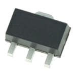
ICGOO电子元器件商城为您提供BGA7024,135由NXP Semiconductors设计生产,在icgoo商城现货销售,并且可以通过原厂、代理商等渠道进行代购。 BGA7024,135价格参考¥18.27-¥18.27。NXP SemiconductorsBGA7024,135封装/规格:RF 放大器, 射频放大器 IC ISM,RFID,WLAN 400MHz ~ 2.7GHz SOT-89-3。您可以下载BGA7024,135参考资料、Datasheet数据手册功能说明书,资料中有BGA7024,135 详细功能的应用电路图电压和使用方法及教程。
NXP USA Inc.生产的RF放大器型号BGA7024,135,是一款高性能射频(RF)晶体管,广泛应用于各种射频通信和无线系统中。以下是其主要应用场景:

 1. 无线通信设备
   - BGA7024,135适用于基站、中继器和其他无线通信设备中的射频功率放大器设计。它能够提供高增益和高效率的信号放大,支持多种无线通信标准,如GSM、LTE、WiMAX等。
   - 在蜂窝网络中,该器件可用于增强信号覆盖范围,提高数据传输速率和可靠性。

 2. 雷达系统
   - 在军事和民用雷达应用中,BGA7024,135可用作发射机的功率放大器。其高频性能和稳定性使其适合于气象雷达、空中交通管制雷达以及地面探测雷达等场景。

 3. 卫星通信
   - 该型号可应用于卫星地面站的上行链路放大器中,确保信号在传输到卫星时具有足够的功率和清晰度。
   - 它还适用于低地球轨道(LEO)和同步轨道(GEO)卫星通信系统的终端设备。

 4. 测试与测量仪器
   - 在实验室环境中,BGA7024,135被用作信号源或功率放大器的核心组件,用于测试射频电路、天线和其他无线设备的性能。
   - 其宽频带特性和高线性度使得它非常适合精密测量任务。

 5. 工业、科学和医疗(ISM)领域
   - 在ISM频段内,这款RF放大器可用于无线能量传输、材料加热、医疗成像等应用。例如,在磁共振成像(MRI)设备中,它可以放大射频脉冲以激发人体组织中的原子核。

 6. 物联网(IoT)和M2M通信
   - 随着物联网设备的普及,BGA7024,135可以为远程传感器节点、网关和路由器提供可靠的射频信号放大功能,支持长距离通信。

 总结
BGA7024,135凭借其出色的射频性能、宽带能力和高可靠性,成为众多射频应用的理想选择。无论是商业通信还是特殊用途的技术开发,这款放大器都能满足严格的技术要求,推动现代无线技术的发展。
| 参数 | 数值 |
| 产品目录 | |
| 描述 | IC MMIC DRIVER AMP 1STAGE SOT89 |
| 产品分类 | |
| 品牌 | NXP Semiconductors |
| 数据手册 | |
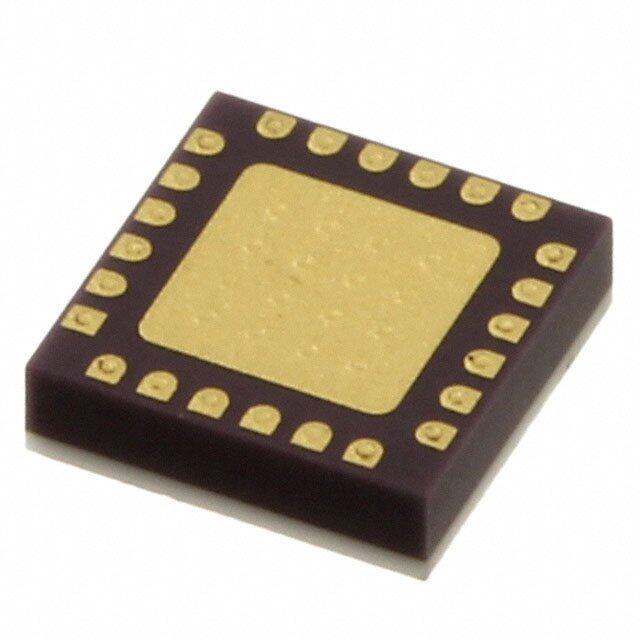
| 产品图片 |
|
| P1dB | 25.5dBm(354.8mW) |
| 产品型号 | BGA7024,135 |
| PCN设计/规格 | |
| RF类型 | ISM,RFID,WLAN |
| rohs | 无铅 / 符合限制有害物质指令(RoHS)规范要求 |
| 产品系列 | - |
| 产品目录页面 | |
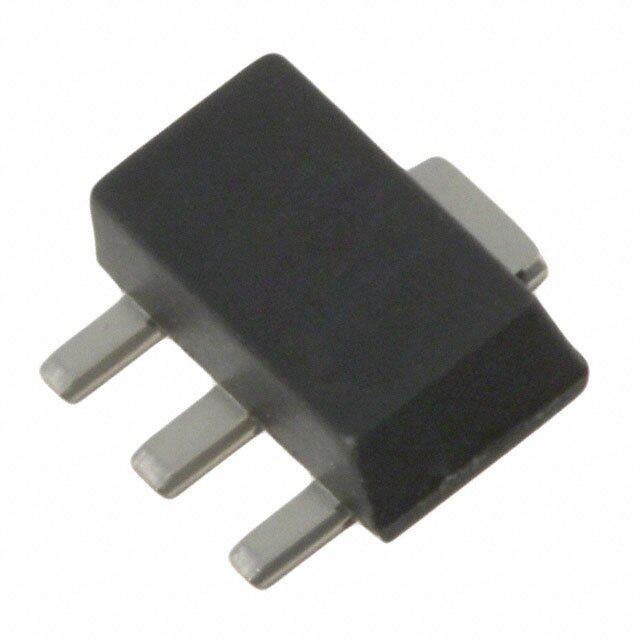
| 供应商器件封装 | SOT-89-3 |
| 其它名称 | 568-5106-6 |
| 包装 | Digi-Reel® |
| 噪声系数 | 3.7dB |
| 增益 | 16dB |
| 封装/外壳 | TO-243AA |
| 标准包装 | 1 |
| 测试频率 | 1.96GHz |
| 电压-电源 | 5V |
| 电流-电源 | 110mA |
| 频率 | 400MHz ~ 2.7GHz |
SOT89.jpg)


- 商务部:美国ITC正式对集成电路等产品启动337调查
- 曝三星4nm工艺存在良率问题 高通将骁龙8 Gen1或转产台积电
- 太阳诱电将投资9.5亿元在常州建新厂生产MLCC 预计2023年完工
- 英特尔发布欧洲新工厂建设计划 深化IDM 2.0 战略
- 台积电先进制程称霸业界 有大客户加持明年业绩稳了
- 达到5530亿美元!SIA预计今年全球半导体销售额将创下新高
- 英特尔拟将自动驾驶子公司Mobileye上市 估值或超500亿美元
- 三星加码芯片和SET,合并消费电子和移动部门,撤换高东真等 CEO
- 三星电子宣布重大人事变动 还合并消费电子和移动部门
- 海关总署:前11个月进口集成电路产品价值2.52万亿元 增长14.8%


PDF Datasheet 数据手册内容提取
BGA7024 (cid:50)(cid:55)(cid:27)(cid:28) (cid:54) 400 MHz to 2700 MHz 0.25 W high linearity silicon amplifier Rev. 3 — 11 June 2014 Product data sheet 1. Product profile 1.1 General description The BGA7024 MMIC is a one-stage amplifier, available in a low-cost surface-mount package. It delivers 24 dBm output power at 1 dB gain compression and superior performance up to 2700MHz. 1.2 Features and benefits 400 MHz to 2700 MHz frequency operating range 16 dB small signal gain at 2 GHz 24 dBm output power at 1 dB gain compression Integrated active biasing External matching allows broad application optimization of the electrical performance 5 V single supply operation All pins ESD protected 1.3 Applications Broadband CPE/MoCA Industrial applications WLAN/ISM/RFID E-metering Wireless infrastructure (base station, Satellite Master Antenna TV (SMATV) repeater, point-to-point backhaul systems) 1.4 Quick reference data Table 1. Quick reference data Input and output impedances matched to 50 . Typical values at V =5V; T =25C; CC case unlessotherwise specified. Symbol Parameter Conditions Min Typ Max Unit I supply current 95 110 125 mA CC f frequency [1] 400 - 2700 MHz G power gain f = 2140 MHz 13.5 15 16.5 dB p P output power at 1 dB gain compression f = 2140 MHz 24.0 25.5 - dBm L(1dB) IP3 output third-order intercept point f = 2140 MHz [2] 35.0 38.5 - dBm O [1] Operation outside this range is possible but not guaranteed. [2] P = 11 dBm per tone; spacing = 1 MHz. L
BGA7024 NXP Semiconductors 400 MHz to 2700 MHz 0.25 W high linearity silicon amplifier 2. Pinning information Table 2. Pinning Pin Description Simplified outline Graphic symbol 1 V [1] CC(RF) 2 GND [2] (cid:22) (cid:20) 3 RF_IN [1] (cid:21) (cid:22) (cid:21) (cid:20) (cid:86)(cid:92)(cid:80)(cid:20)(cid:22)(cid:19) [1] This pin is DC-coupled and requires an external DC-blocking capacitor. [2] The center metal base of the SOT89 also functions as heatsink for the power amplifier. 3. Ordering information Table 3. Ordering information Type number Package Name Description Version BGA7024 - plastic surface-mounted package; exposed die pad for good SOT89 heattransfer; 3 leads 4. Functional diagram BIAS V/I BANDGAP ENABLE CONVERTER 3 1 RF_IN VCC(RF) 2 GND 014aab020 Fig 1. Functional diagram BGA7024 All information provided in this document is subject to legal disclaimers. © NXP Semiconductors N.V. 2014. All rights reserved. Product data sheet Rev. 3 — 11 June 2014 2 of 23
BGA7024 NXP Semiconductors 400 MHz to 2700 MHz 0.25 W high linearity silicon amplifier 5. Limiting values Table 4. Limiting valu es In accordance with the Absolute Maximum Rating System (IEC 60134). Symbol Parameter Conditions Min Max Unit V RF supply voltage - 5.7 V CC(RF) P RF input power - 25 dBm i(RF) T case temperature 40 +85 C case T junction temperature - 150 C j V electrostatic discharge voltage HumanBodyModel(HBM); - 2000 V ESD accordingtoJEDECstandard22-A114E Charged DeviceModel(CDM); - 500 V accordingto JEDECstandard22-C101B 6. Thermal characteristics Table 5. Thermal characteristics Symbol Parameter Conditions Typ Unit R thermal resistance from junction to case [1][2] 25 K/W th(j-c) [1] Case is ground solder pad. [2] Thermal resistance measured using infrared measurement technique, device mounted on application board and placed in still air. 7. Static characteristics Table 6. Characteristics Input and output impedances matched to 50 . Typical values at V =5V; T =25C; unless CC case otherwise specified. Symbol Parameter Conditions Min Typ Max Unit V supply voltage - 5.0 - V CC I supply current 95 110 125 mA CC 8. Dynamic characteristics Table 7. Dynamic characteristics Input and output impedances matched to 50 . Typical values at V =5V; T =25C; see CC case Section 12 “Application information”; unless otherwise specified. Symbol Parameter Conditions Min Typ Max Unit f frequency [1] 400 - 2700 MHz G power gain f = 940 MHz - 22 - dB p f = 1960 MHz - 16 - dB f = 2140 MHz 13.5 15 16.5 dB f = 2445 MHz - 14 - dB BGA7024 All information provided in this document is subject to legal disclaimers. © NXP Semiconductors N.V. 2014. All rights reserved. Product data sheet Rev. 3 — 11 June 2014 3 of 23
BGA7024 NXP Semiconductors 400 MHz to 2700 MHz 0.25 W high linearity silicon amplifier Table 7. Dynamic characteristics …continued Input and output impedances matched to 50 . Typical values at V =5V; T =25C; see CC case Section 12 “Application information”; unless otherwise specified. Symbol Parameter Conditions Min Typ Max Unit P output power at 1 dB gain compression f = 940 MHz - 24 - dBm L(1dB) f = 1960 MHz - 25.5 - dBm f = 2140 MHz 24.0 25.5 - dBm f = 2445 MHz - 24.5 - dBm IP3 output third-order intercept point f = 940 MHz [2] - 37.5 - dBm O f = 1960 MHz [2] - 38.0 - dBm f = 2140 MHz [2] 35.0 38.0 - dBm f = 2445 MHz [2] - 37.5 - dBm NF noise figure f = 940 MHz [3] - 2.9 - dB f = 1960 MHz [3] - 3.7 - dB f = 2140 MHz [3] - 3.7 - dB f = 2445 MHz [3] - 4.0 - dB RL input return loss f = 940 MHz - 9 - dB in f = 1960 MHz - 10 - dB f = 2140 MHz - 10 - dB f = 2445 MHz - 14 - dB RL output return loss f = 940 MHz - 29 - dB out f = 1960 MHz - 22 - dB f = 2140 MHz - 29 - dB f = 2445 MHz - 11 - dB [1] Operation outside this range is possible but not guaranteed. [2] P = 11 dBm per tone; spacing = 1 MHz. L [3] Defined at Pi(RF) = 40 dBm; small signal conditions. 9. Scattering parameters Table 8. Scattering pa rameters at 5V, MMIC only f (MHz) S S S S 11 21 12 22 Magnitude Angle Magnitude Angle Magnitude Angle Magnitude Angle (ratio) (degree) (ratio) (degree) (ratio) (degree) (ratio) (degree) 400 0.83 178.9 14.03 112.7 0.01 35.5 0.53 166.3 500 0.85 178.7 11.69 104.4 0.01 38.77 0.56 168.9 600 0.85 176.4 9.93 98.19 0.02 41.13 0.57 172.2 700 0.86 173.8 8.67 93.04 0.02 43.1 0.58 174.8 800 0.86 171.1 7.68 88.54 0.02 44.34 0.58 177.4 900 0.86 168.3 6.9 84.36 0.02 44.96 0.59 179.7 1000 0.86 165.4 6.29 80.24 0.02 45.07 0.60 176.7 1100 0.87 162.7 5.72 76.42 0.02 45 0.60 173.3 1200 0.88 159.9 5.23 72.83 0.02 44.54 0.60 170.9 1300 0.88 157.3 4.80 69.34 0.03 44.17 0.61 168.4 BGA7024 All information provided in this document is subject to legal disclaimers. © NXP Semiconductors N.V. 2014. All rights reserved. Product data sheet Rev. 3 — 11 June 2014 4 of 23
BGA7024 NXP Semiconductors 400 MHz to 2700 MHz 0.25 W high linearity silicon amplifier Table 8. Scattering parameters at 5V, MMIC only …continued f (MHz) S S S S 11 21 12 22 Magnitude Angle Magnitude Angle Magnitude Angle Magnitude Angle (ratio) (degree) (ratio) (degree) (ratio) (degree) (ratio) (degree) 1400 0.89 154.8 4.43 66.17 0.03 43.58 0.61 166.4 1500 0.89 153 4.09 63.33 0.03 43.02 0.62 164.7 1600 0.89 151.3 3.80 60.8 0.03 42.67 0.63 163.1 1700 0.90 149.9 3.54 58.3 0.03 42.36 0.64 162.1 1800 0.90 148.7 3.30 56.13 0.03 41.89 0.65 161.2 1900 0.90 147.9 3.11 54.13 0.03 41.65 0.66 160.8 2000 0.91 147.5 2.93 52.63 0.03 41.7 0.66 160.5 2100 0.90 147 2.78 50.91 0.04 41.61 0.66 160.5 2200 0.90 146.9 2.65 49.5 0.04 41.59 0.67 160.9 2300 0.90 146.6 2.54 48.13 0.04 41.44 0.66 161.6 2400 0.90 146.5 2.46 46.88 0.04 41.61 0.66 161.7 2500 0.89 146.3 2.39 45.39 0.04 41.45 0.66 162.6 2600 0.88 146 2.34 43.93 0.05 41.13 0.65 162.8 2700 0.87 145.4 2.30 42.24 0.05 40.56 0.64 163.2 10. Reliability information Table 9. Reliability Life test Conditions Intrinsic failure rate HTOL according to JESD85; confidence level 60 %; T =55C; 4 j activationenergy=0.7eV; acceleration factor according to Arrhenius equation 11. Moisture sensitivity Table 10. Moisture sensitivity level Test methodology Class JESD-22-A113 1 BGA7024 All information provided in this document is subject to legal disclaimers. © NXP Semiconductors N.V. 2014. All rights reserved. Product data sheet Rev. 3 — 11 June 2014 5 of 23
BGA7024 NXP Semiconductors 400 MHz to 2700 MHz 0.25 W high linearity silicon amplifier 12. Application information 12.1 920 MHz to 960 MHz J3 R1 C7 VCC C6 C8 L3 L2 C9 50 Ω MSL1 C1 MSL2 MSL3 RF_IN VCC(RF) MSL4 L1 MSL5 C5 MSL6 50 Ω J1 J2 C2 C3 BGA7024 C4 014aab021 See Table11 for a list of components. PCB specification: Rogers RO4003C; height = 0.508 mm; r = 3.38; copper thickness = 35 m. Fig 2. 5 V application schematic; 920 MHz to 960 MHz 014aab022 014aab023 30 28 PL(1dB) Gp (dBm) (dB) 28 26 26 24 (1) (1) (2) (2) 24 22 (3) (3) 22 20 20 18 0.92 0.93 0.94 0.95 0.96 0.92 0.93 0.94 0.95 0.96 f (GHz) f (GHz) (1) Tcase = 40 C. (1) Tcase = 40 C. (2) Tcase = 25 C. (2) Tcase = 25 C. (3) Tcase = 85 C. (3) Tcase = 85 C. Fig 3. Output power at 1 dB gain compression as a Fig 4. Power gain as a function of frequency function of frequency BGA7024 All information provided in this document is subject to legal disclaimers. © NXP Semiconductors N.V. 2014. All rights reserved. Product data sheet Rev. 3 — 11 June 2014 6 of 23
BGA7024 NXP Semiconductors 400 MHz to 2700 MHz 0.25 W high linearity silicon amplifier 014aab024 014aab025 0 42 RLin, RLout, ISL IP3O (dB) (dBm) 40 (1) −10 (2) 38 (3) (1) 36 −20 (2) 34 (3) −30 32 0.92 0.93 0.94 0.95 0.96 0.92 0.93 0.94 0.95 0.96 f (GHz) f (GHz) Tcase = 25 C. (1) Tcase = 40 C. (1) RLin (2) Tcase = 25 C. (2) RLout (3) Tcase = 85 C. (3) ISL Fig 5. Input return loss, output return loss and Fig 6. Output third-order intercept point as a function isolation as a function of frequency of frequency G G G V G G N N N C N N D D D C D D J3 C8 R1 C7 J1 J2 C6 L3 C9 L1 L2 MSL1 C1 MSL2 MSL3 MSL5 C5 MSL6 C2 C3 C4 J I HGFEDCBA 12345678910 12 MSL4 11 13 RF in RF out 014aab026 See Table11 for a list of components. Fig 7. 5 V application reference board; 920 MHz to 960 MHz BGA7024 All information provided in this document is subject to legal disclaimers. © NXP Semiconductors N.V. 2014. All rights reserved. Product data sheet Rev. 3 — 11 June 2014 7 of 23
BGA7024 NXP Semiconductors 400 MHz to 2700 MHz 0.25 W high linearity silicon amplifier Table 11. 5 V applicati on list of components; 920 MHz to 960 MHz See Figure2 and Figure7 for component layout. PCB: Rogers RO4003C stack; height = 0.508 mm; copper plating thickness=35m. Component Description Value Function Remarks C1, C5 capacitor 68 pF DC blocking Murata GRM1885C1H680JA01D C2 capacitor 3.9 pF input match Murata GRM1885C1H3R9CZ01D C3 capacitor 3.9 pF input match Murata GRM1885C1H3R9CZ01D C4 capacitor 3.9 pF output match Murata GRM1885C1H3R9CZ01D C6 capacitor 68 pF RF decoupling Murata GRM1885C1H680JA01D C7 capacitor 100 nF DC decoupling AVX 0603YC104KAT2A C8 capacitor 10 F DC decoupling AVX 1206ZG106ZAT2A C9 capacitor 68 nF IMD Murata GRM1888R71H683KA93D suppression J1, J2 RF connector SMA - Emerson Network Power 142-0701-841 J3 DC connector 6-pins - MOLEX L1 inductor 4.7 nH output match Tyco Electronics 36501J4N7JTDG L2 inductor 22 nH DC feed Tyco Electronics 36501J022JTDG L3 inductor 33 nH IMD Tyco Electronics 36501J033JTDG suppression MSL1[1] micro stripline 1.14mm0.8mm10.95mm input match - MSL2[1] micro stripline 1.14mm0.8mm5.65mm input match - MSL3[1] micro stripline 1.14mm0.8mm6.1mm input match - MSL4[1] micro stripline 1.14mm0.8mm1.6mm output match - MSL5[1] micro stripline 1.14mm0.8mm8.4mm output match - MSL6[1] micro stripline 1.14mm0.8mm10.95 mm output match - R1 resistor 0 - Multicomp MC0.063W06030R PCB - RO4003C - - [1] MSL1 to MSL6 dimensions specified as width spacing length. 12.2 1930 MHz to 1990 MHz J3 R1 C6 VCC C5 C7 L1 50 Ω MSL1 C1 MSL2 MSL3 RF_IN VCC(RF) MSL4 MSL5 MSL6 C4 MSL7 50 Ω J1 J2 C2 BGA7024 C3 014aab027 See Table12 for a list of components. PCB specification: Rogers RO4003C; height = 0.508 mm; r = 3.38; copper thickness = 35 m. Fig 8. 5 V application schematic; 1930 MHz to 1990 MHz BGA7024 All information provided in this document is subject to legal disclaimers. © NXP Semiconductors N.V. 2014. All rights reserved. Product data sheet Rev. 3 — 11 June 2014 8 of 23
BGA7024 NXP Semiconductors 400 MHz to 2700 MHz 0.25 W high linearity silicon amplifier 014aab028 014aab029 30 20 PL(1dB) Gp (dBm) (dB) 28 18 (1) (2) (1) 26 (2) 16 (3) (3) 24 14 22 12 20 10 1.93 1.95 1.97 1.99 1.93 1.95 1.97 1.99 f (GHz) f (GHz) (1) Tcase = 40 C. (1) Tcase = 40 C. (2) Tcase = 25 C. (2) Tcase = 25 C. (3) Tcase = 85 C. (3) Tcase = 85 C. Fig 9. Output power at 1 dB gain compression as a Fig 10. Power gain as a function of frequency function of frequency 014aab030 014aab031 0 42 RLin, RLout, ISL IP3O (dB) (dBm) 40 (1) (1) (2) −10 38 (3) 36 −20 (2) (3) 34 −30 32 1.93 1.95 1.97 1.99 1.93 1.95 1.97 1.99 f (GHz) f (GHz) Tcase = 25 C. (1) Tcase = 40 C. (1) RLin (2) Tcase = 25 C. (2) RLout (3) Tcase = 85 C. (3) ISL Fig 11. Input return loss, output return loss and Fig 12. Output third-order intercept point as a function isolation as a function of frequency of frequency BGA7024 All information provided in this document is subject to legal disclaimers. © NXP Semiconductors N.V. 2014. All rights reserved. Product data sheet Rev. 3 — 11 June 2014 9 of 23
BGA7024 NXP Semiconductors 400 MHz to 2700 MHz 0.25 W high linearity silicon amplifier G G G V G G N N N C N N D D D C D D J3 C7 R1 C6 J1 J2 MSL4 MSL3 C5 MSL5 L1 MSL1 C1 MSL2 MSL6 C4 MSL7 C2 C3 J I HGFEDCBA 12345678910 12 11 13 RF in RF out 014aab032 See Table12 for a list of components. Fig 13. 5 V application reference board; 1930 MHz to 1990 MHz BGA7024 All information provided in this document is subject to legal disclaimers. © NXP Semiconductors N.V. 2014. All rights reserved. Product data sheet Rev. 3 — 11 June 2014 10 of 23
BGA7024 NXP Semiconductors 400 MHz to 2700 MHz 0.25 W high linearity silicon amplifier Table 12. 5 V applicati on list of components; 1930 MHz to 1990 MHz See Figure8 and Figure13 for component layout. PCB: Rogers RO4003C stack; height = 0.508 mm; copper plating thickness =35m. Component Description Value Function Remarks C1, C4 capacitor 15 pF DC blocking Murata GRM1885C1H150JA01D C2 capacitor 2.4 pF input match Murata GRM1885C1H2R4CZ01D C3 capacitor 1.5 pF output match Murata GRM1885C1H1R5CZ01D C5 capacitor 15 pF RF decoupling Murata GRM1885C1H150JA01D C6 capacitor 100 nF DC decoupling AVX 0603YC104KAT2A C7 capacitor 10 F DC decoupling AVX 1206ZG106ZAT2A J1, J2 RF connector SMA - Emerson Network Power 142-0701-841 J3 DC connector 6-pins - MOLEX L1 inductor 22 nH DC feed Tyco Electronics 36501J022JTDG MSL1[1] micro stripline 1.14mm0.8mm10.95mm input match - MSL2[1] micro stripline 1.14mm0.8mm10.6mm input match - MSL3[1] micro stripline 1.14mm0.8mm1.0 mm input match - MSL4[1] micro stripline 1.14mm0.8mm2.7mm output match - MSL5[1] micro stripline 1.14mm0.8mm3.2mm output match - MSL6[1] micro stripline 1.14mm0.8mm5.5mm output match - MSL7[1] micro stripline 1.14mm0.8mm10.95mm output match - R1 resistor 0 - Multicomp MC 0.063W 0603 0R PCB - RO4003C - - [1] MSL1 to MSL7 dimensions specified as width spacing length. 12.3 2110 MHz to 2170 MHz J3 R1 C6 VCC C5 C7 L1 50 Ω MSL1 C1 MSL2 MSL3 RF_IN VCC(RF) MSL4 MSL5 MSL6 C4 MSL7 50 Ω J1 J2 C2 BGA7024 C3 014aab033 See Table13 for a list of components. PCB specification: Rogers RO4003C; height = 0.508 mm; r = 3.38; copper thickness = 35 m. Fig 14. 5 V application schematic; 2110 MHz to 2170 MHz BGA7024 All information provided in this document is subject to legal disclaimers. © NXP Semiconductors N.V. 2014. All rights reserved. Product data sheet Rev. 3 — 11 June 2014 11 of 23
BGA7024 NXP Semiconductors 400 MHz to 2700 MHz 0.25 W high linearity silicon amplifier 014aab034 014aab035 30 20 PL(1dB) Gp (dBm) (dB) 28 18 (1) (2) (1) 26 16 (2) (3) (3) 24 14 22 12 20 10 2.11 2.13 2.15 2.17 2.11 2.13 2.15 2.17 f (GHz) f (GHz) (1) Tcase = 40 C. (1) Tcase = 40 C. (2) Tcase = 25 C. (2) Tcase = 25 C. (3) Tcase = 85 C. (3) Tcase = 85 C. Fig 15. Output power at 1 dB gain compression as a Fig 16. Power gain as a function of frequency function of frequency 014aab036 014aab037 0 42 RLin, RLout, ISL IP3O (dB) (dBm) 40 −10 (1) 38 (1) (2) 36 (3) −20 (2) (3) 34 −30 32 2.11 2.13 2.15 2.17 2.11 2.13 2.15 2.17 f (GHz) f (GHz) Tcase = 25 C. (1) Tcase = 40 C. (1) RLin (2) Tcase = 25 C. (2) RLout (3) Tcase = 85 C. (3) ISL Fig 17. Input return loss, output return loss and Fig 18. Output third-order intercept point as a function isolation as a function of frequency of frequency BGA7024 All information provided in this document is subject to legal disclaimers. © NXP Semiconductors N.V. 2014. All rights reserved. Product data sheet Rev. 3 — 11 June 2014 12 of 23
BGA7024 NXP Semiconductors 400 MHz to 2700 MHz 0.25 W high linearity silicon amplifier G G G V G G N N N C N N D D D C D D J3 C7 R1 C6 J1 J2 MSL4 MSL3 C5 MSL5 L1 MSL1 C1 MSL2 MSL6 C4 MSL7 C2 C3 J I HGFEDCBA 12345678910 12 11 13 RF in RF out 014aab038 See Table13 for a list of components. Fig 19. 5 V application reference board; 2110 MHz to 2170 MHz BGA7024 All information provided in this document is subject to legal disclaimers. © NXP Semiconductors N.V. 2014. All rights reserved. Product data sheet Rev. 3 — 11 June 2014 13 of 23
BGA7024 NXP Semiconductors 400 MHz to 2700 MHz 0.25 W high linearity silicon amplifier Table 13. 5 V applicati on list of components; 2110 MHz to 2170 MHz See Figure14 and Figure19 for component layout. PCB: Rogers RO4003C stack; height = 0.508 mm; copper plating thickness=35m. Component Description Value Function Remarks C1, C4 capacitor 15 pF DC blocking Murata GRM1885C1H150JA01D C2 capacitor 2.2 pF input match Murata GRM1885C1H2R2CZ01D C3 capacitor 1.5 pF output match Murata GRM1885C1H1R5CZ01D C5 capacitor 15 pF RF decoupling Murata GRM1885C1H150JA01D C6 capacitor 100 nF DC decoupling AVX 0603YC104KAT2A C7 capacitor 10 F DC decoupling AVX 1206ZG106ZAT2A J1, J2 RF connector SMA - Emerson Network Power 142-0701-841 J3 DC connector 6-pins - MOLEX L1 inductor 22 nH DC feed Tyco Electronics 36501J022JTDG MSL1[1] micro stripline 1.14mm0.8mm10.95mm input match - MSL2[1] micro stripline 1.14mm0.8mm10.6mm input match - MSL3[1] micro stripline 1.14mm0.8mm1.0mm input match - MSL4[1] micro stripline 1.14mm0.8mm2.7mm output match - MSL5[1] micro stripline 1.14mm0.8mm3.2mm output match - MSL6[1] micro stripline 1.14mm0.8mm5.5mm output match - MSL7[1] micro stripline 1.14mm0.8mm10.95mm output match - R1 resistor 0 - Multicomp MC 0.063W 0603 0R PCB - RO4003C - - [1] MSL1 to MSL7 dimensions specified as width spacing length. 12.4 2405 MHz to 2485 MHz J3 R1 C6 VCC C5 C7 L2 50 Ω MSL1 C1 MSL2 MSL3 RF_IN VCC(RF) MSL4 MSL5 MSL6 C4 MSL7 50 Ω J1 J2 L1 C2 BGA7024 C3 014aab039 See Table14 for a list of components. PCB specification: Rogers RO4003C; height = 0.508 mm; r = 3.38; copper thickness = 35 m. Fig 20. 5 V application schematic; 2405 MHz to 2485 MHz BGA7024 All information provided in this document is subject to legal disclaimers. © NXP Semiconductors N.V. 2014. All rights reserved. Product data sheet Rev. 3 — 11 June 2014 14 of 23
BGA7024 NXP Semiconductors 400 MHz to 2700 MHz 0.25 W high linearity silicon amplifier 014aab040 014aab041 30 20 PL(1dB) Gp (dBm) (dB) 28 18 26 16 (1) (1) 24 14 (2) (2) (3) (3) 22 12 20 10 2.405 2.425 2.445 2.465 2.485 2.405 2.425 2.445 2.465 2.485 f (GHz) f (GHz) (1) Tcase = 40 C. (1) Tcase = 40 C. (2) Tcase = 25 C. (2) Tcase = 25 C. (3) Tcase = 85 C. (3) Tcase = 85 C. Fig 21. Output power at 1 dB gain compression as a Fig 22. Power gain as a function of frequency function of frequency 014aab042 014aab043 0 42 IP3O RLin, RLout, ISL (dBm) (dB) 40 −10 (2) (2) 38 (3) (1) (1) 36 −20 (3) 34 −30 32 2.405 2.425 2.445 2.465 2.485 2.405 2.425 2.445 2.465 2.485 f (GHz) f (GHz) Tcase = 25 C. (1) Tcase = 40 C. (1) RLin (2) Tcase = 25 C. (2) RLout (3) Tcase = 85 C. (3) ISL Fig 23. Input return loss, output return loss and Fig 24. Output third-order intercept point as a function isolation as a function of frequency of frequency BGA7024 All information provided in this document is subject to legal disclaimers. © NXP Semiconductors N.V. 2014. All rights reserved. Product data sheet Rev. 3 — 11 June 2014 15 of 23
BGA7024 NXP Semiconductors 400 MHz to 2700 MHz 0.25 W high linearity silicon amplifier G G G V G G N N N C N N D D D C D D J3 C7 R1 C6 J1 J2 MSL4 MSL3 C5 MSL5 L2 MSL1 C1 MSL2 MSL6 C4 MSL7 L1 C2 C3 J I HGFEDCBA 12345678910 12 11 13 RF in RF out 014aab044 See Table14 for a list of components. Fig 25. 5 V application reference board; 2405 MHz to 2485 MHz BGA7024 All information provided in this document is subject to legal disclaimers. © NXP Semiconductors N.V. 2014. All rights reserved. Product data sheet Rev. 3 — 11 June 2014 16 of 23
BGA7024 NXP Semiconductors 400 MHz to 2700 MHz 0.25 W high linearity silicon amplifier Table 14. 5 V applicati on list of components; 2405 MHz to 2485 MHz See Figure20 and Figure25 for component layout. PCB: Rogers RO4003C stack; height = 0.508 mm; copper plating thickness=35m. Component Description Value Function Remarks C1, C4 capacitor 15 pF DC blocking Murata GRM1885C1H150JA01D C2 capacitor 1.5 pF input match Murata GRM1885C1H1R5CZ01D C3 capacitor 1.8 pF output match Murata GRM1885C1H1R8CZ01D C5 capacitor 15 pF RF decoupling Murata GRM1885C1H150JA01D C6 capacitor 100 nF DC decoupling AVX 0603YC104KAT2A C7 capacitor 10 F DC decoupling AVX 1206ZG106ZAT2A J1, J2 RF connector SMA - Emerson Network Power 142-0701-841 J3 DC connector 6-pins - MOLEX L1 inductor 3.3 nH input match Tyco Electronics 36501J3N3JTDG L2 inductor 22 nH DC feed Tyco Electronics 36501J022JTDG MSL1[1] micro stripline 1.14mm0.8mm10.95mm input match - MSL2[1] micro stripline 1.14mm0.8mm9.8mm input match - MSL3[1] micro stripline 1.14mm0.8mm1.9mm output match - MSL4[1] micro stripline 1.14mm0.8mm2.5mm output match - MSL5[1] micro stripline 1.14mm0.8mm1.6mm output match - MSL6[1] micro stripline 1.14mm0.8mm7.3mm output match - MSL7[1] micro stripline 1.14mm0.8mm10.95mm output match - R1 resistor 0 - Multicomp MC 0.063W 0603 0R PCB - RO4003C - - [1] MSL1 to MSL7 dimensions specified as width spacing length. BGA7024 All information provided in this document is subject to legal disclaimers. © NXP Semiconductors N.V. 2014. All rights reserved. Product data sheet Rev. 3 — 11 June 2014 17 of 23
BGA7024 NXP Semiconductors 400 MHz to 2700 MHz 0.25 W high linearity silicon amplifier 12.5 PCB stack through via RF & analog routing 35 μm (1 oz.) copper + 0.3 μm gold plating RO4003C, 0.51 mm (20 mil) RF & analog ground 35 μm (1 oz.) copper (1) 0.2 mm (8 mil) analog routing 35 μm (1 oz.) copper FR4, 0.15 mm (6 mil) RF & analog ground 35 μm (1 oz.) copper 014aab045 (1) Pre-impregnated. RO4003C dielectric constant r = 3.38. Fig 26. PCB stack BGA7024 All information provided in this document is subject to legal disclaimers. © NXP Semiconductors N.V. 2014. All rights reserved. Product data sheet Rev. 3 — 11 June 2014 18 of 23
BGA7024 NXP Semiconductors 400 MHz to 2700 MHz 0.25 W high linearity silicon amplifier 13. Package outline (cid:51)(cid:79)(cid:68)(cid:86)(cid:87)(cid:76)(cid:70)(cid:3)(cid:86)(cid:88)(cid:85)(cid:73)(cid:68)(cid:70)(cid:72)(cid:16)(cid:80)(cid:82)(cid:88)(cid:81)(cid:87)(cid:72)(cid:71)(cid:3)(cid:83)(cid:68)(cid:70)(cid:78)(cid:68)(cid:74)(cid:72)(cid:30)(cid:3)(cid:72)(cid:91)(cid:83)(cid:82)(cid:86)(cid:72)(cid:71)(cid:3)(cid:71)(cid:76)(cid:72)(cid:3)(cid:83)(cid:68)(cid:71)(cid:3)(cid:73)(cid:82)(cid:85)(cid:3)(cid:74)(cid:82)(cid:82)(cid:71)(cid:3)(cid:75)(cid:72)(cid:68)(cid:87)(cid:3)(cid:87)(cid:85)(cid:68)(cid:81)(cid:86)(cid:73)(cid:72)(cid:85)(cid:30)(cid:3)(cid:22)(cid:3)(cid:79)(cid:72)(cid:68)(cid:71)(cid:86) (cid:54)(cid:50)(cid:55)(cid:27)(cid:28) (cid:39) (cid:37) (cid:36) (cid:69)(cid:83)(cid:22) (cid:40) (cid:43)(cid:40) (cid:47)(cid:83) (cid:20) (cid:21) (cid:22) (cid:69)(cid:83)(cid:21) (cid:70) (cid:90) (cid:48) (cid:37) (cid:69)(cid:83)(cid:20) (cid:72)(cid:20) (cid:72) (cid:19) (cid:21) (cid:23)(cid:3)(cid:80)(cid:80) (cid:86)(cid:70)(cid:68)(cid:79)(cid:72) (cid:39)(cid:44)(cid:48)(cid:40)(cid:49)(cid:54)(cid:44)(cid:50)(cid:49)(cid:54)(cid:3)(cid:11)(cid:80)(cid:80)(cid:3)(cid:68)(cid:85)(cid:72)(cid:3)(cid:87)(cid:75)(cid:72)(cid:3)(cid:82)(cid:85)(cid:76)(cid:74)(cid:76)(cid:81)(cid:68)(cid:79)(cid:3)(cid:71)(cid:76)(cid:80)(cid:72)(cid:81)(cid:86)(cid:76)(cid:82)(cid:81)(cid:86)(cid:12) (cid:56)(cid:49)(cid:44)(cid:55) (cid:36) (cid:69)(cid:83)(cid:20) (cid:69)(cid:83)(cid:21) (cid:69)(cid:83)(cid:22) (cid:70) (cid:39) (cid:40) (cid:72) (cid:72)(cid:20) (cid:43)(cid:40) (cid:47)(cid:83) (cid:90) (cid:20)(cid:17)(cid:25)(cid:3) (cid:19)(cid:17)(cid:23)(cid:27)(cid:3) (cid:19)(cid:17)(cid:24)(cid:22)(cid:3) (cid:20)(cid:17)(cid:27)(cid:3) (cid:19)(cid:17)(cid:23)(cid:23)(cid:3) (cid:23)(cid:17)(cid:25)(cid:3) (cid:21)(cid:17)(cid:25)(cid:3) (cid:23)(cid:17)(cid:21)(cid:24)(cid:3) (cid:20)(cid:17)(cid:21)(cid:3) (cid:80)(cid:80) (cid:22)(cid:17)(cid:19) (cid:20)(cid:17)(cid:24) (cid:19)(cid:17)(cid:20)(cid:22) (cid:20)(cid:17)(cid:23) (cid:19)(cid:17)(cid:22)(cid:24) (cid:19)(cid:17)(cid:23)(cid:19) (cid:20)(cid:17)(cid:23) (cid:19)(cid:17)(cid:21)(cid:22) (cid:23)(cid:17)(cid:23) (cid:21)(cid:17)(cid:23) (cid:22)(cid:17)(cid:26)(cid:24) (cid:19)(cid:17)(cid:27) (cid:50)(cid:56)(cid:55)(cid:47)(cid:44)(cid:49)(cid:40)(cid:3) (cid:3)(cid:53)(cid:40)(cid:41)(cid:40)(cid:53)(cid:40)(cid:49)(cid:38)(cid:40)(cid:54) (cid:40)(cid:56)(cid:53)(cid:50)(cid:51)(cid:40)(cid:36)(cid:49)(cid:3) (cid:44)(cid:54)(cid:54)(cid:56)(cid:40)(cid:3)(cid:39)(cid:36)(cid:55)(cid:40) (cid:57)(cid:40)(cid:53)(cid:54)(cid:44)(cid:50)(cid:49) (cid:3)(cid:44)(cid:40)(cid:38) (cid:3)(cid:45)(cid:40)(cid:39)(cid:40)(cid:38) (cid:3)(cid:45)(cid:40)(cid:44)(cid:55)(cid:36) (cid:51)(cid:53)(cid:50)(cid:45)(cid:40)(cid:38)(cid:55)(cid:44)(cid:50)(cid:49) (cid:19)(cid:25)(cid:16)(cid:19)(cid:22)(cid:16)(cid:20)(cid:25)(cid:3) (cid:3)(cid:54)(cid:50)(cid:55)(cid:27)(cid:28) (cid:55)(cid:50)(cid:16)(cid:21)(cid:23)(cid:22) (cid:54)(cid:38)(cid:16)(cid:25)(cid:21) (cid:19)(cid:25)(cid:16)(cid:19)(cid:27)(cid:16)(cid:21)(cid:28) Fig 27. Package outline SOT89 BGA7024 All information provided in this document is subject to legal disclaimers. © NXP Semiconductors N.V. 2014. All rights reserved. Product data sheet Rev. 3 — 11 June 2014 19 of 23
BGA7024 NXP Semiconductors 400 MHz to 2700 MHz 0.25 W high linearity silicon amplifier 14. Abbreviations Table 15. Abbreviations Acronym Description CPE Customer-Premises Equipment ESD ElectroStatic Discharge HTOL High Temperature Operating Life IR InfraRed ISM Industrial, Scientific and Medical MMIC Monolithic Microwave Integrated Circuit MoCA Multimedia over Coax Alliance PCB Printed-Circuit Board RFID Radio Frequency IDentification TX Transmit WLAN Wireless Local Area Network 15. Revision history Table 16. Revision history Document ID Release date Data sheet status Change notice Supersedes BGA7024 v.3 20140611 Product data sheet - BGA7024 v.2 Modifications: • Table5 on page3: Thermal simulation results have been replaced by IR measurements results. BGA7024 v.2 20100830 Product data sheet - BGA7024 v.1 BGA7024 20100528 Product data sheet - - BGA7024 All information provided in this document is subject to legal disclaimers. © NXP Semiconductors N.V. 2014. All rights reserved. Product data sheet Rev. 3 — 11 June 2014 20 of 23
BGA7024 NXP Semiconductors 400 MHz to 2700 MHz 0.25 W high linearity silicon amplifier 16. Legal information 16.1 Data sheet status Document status[1][2] Product status[3] Definition Objective [short] data sheet Development This document contains data from the objective specification for product development. Preliminary [short] data sheet Qualification This document contains data from the preliminary specification. Product [short] data sheet Production This document contains the product specification. [1] Please consult the most recently issued document before initiating or completing a design. [2] The term ‘short data sheet’ is explained in section “Definitions”. [3] The product status of device(s) described in this document may have changed since this document was published and may differ in case of multiple devices. The latest product status information is available on the Internet at URLhttp://www.nxp.com. 16.2 Definitions Suitability for use — NXP Semiconductors products are not designed, authorized or warranted to be suitable for use in life support, life-critical or safety-critical systems or equipment, nor in applications where failure or Draft — The document is a draft version only. The content is still under malfunction of an NXP Semiconductors product can reasonably be expected internal review and subject to formal approval, which may result in to result in personal injury, death or severe property or environmental modifications or additions. NXP Semiconductors does not give any damage. NXP Semiconductors and its suppliers accept no liability for representations or warranties as to the accuracy or completeness of inclusion and/or use of NXP Semiconductors products in such equipment or information included herein and shall have no liability for the consequences of applications and therefore such inclusion and/or use is at the customer’s own use of such information. risk. Short data sheet — A short data sheet is an extract from a full data sheet Applications — Applications that are described herein for any of these with the same product type number(s) and title. A short data sheet is intended products are for illustrative purposes only. NXP Semiconductors makes no for quick reference only and should not be relied upon to contain detailed and representation or warranty that such applications will be suitable for the full information. For detailed and full information see the relevant full data specified use without further testing or modification. sheet, which is available on request via the local NXP Semiconductors sales office. In case of any inconsistency or conflict with the short data sheet, the Customers are responsible for the design and operation of their applications full data sheet shall prevail. and products using NXP Semiconductors products, and NXP Semiconductors accepts no liability for any assistance with applications or customer product Product specification — The information and data provided in a Product design. It is customer’s sole responsibility to determine whether the NXP data sheet shall define the specification of the product as agreed between Semiconductors product is suitable and fit for the customer’s applications and NXP Semiconductors and its customer, unless NXP Semiconductors and products planned, as well as for the planned application and use of customer have explicitly agreed otherwise in writing. In no event however, customer’s third party customer(s). Customers should provide appropriate shall an agreement be valid in which the NXP Semiconductors product is design and operating safeguards to minimize the risks associated with their deemed to offer functions and qualities beyond those described in the applications and products. Product data sheet. NXP Semiconductors does not accept any liability related to any default, damage, costs or problem which is based on any weakness or default in the 16.3 Disclaimers customer’s applications or products, or the application or use by customer’s third party customer(s). Customer is responsible for doing all necessary testing for the customer’s applications and products using NXP Limited warranty and liability — Information in this document is believed to Semiconductors products in order to avoid a default of the applications and be accurate and reliable. However, NXP Semiconductors does not give any the products or of the application or use by customer’s third party representations or warranties, expressed or implied, as to the accuracy or customer(s). NXP does not accept any liability in this respect. completeness of such information and shall have no liability for the consequences of use of such information. NXP Semiconductors takes no Limiting values — Stress above one or more limiting values (as defined in responsibility for the content in this document if provided by an information the Absolute Maximum Ratings System of IEC60134) will cause permanent source outside of NXP Semiconductors. damage to the device. Limiting values are stress ratings only and (proper) operation of the device at these or any other conditions above those given in In no event shall NXP Semiconductors be liable for any indirect, incidental, the Recommended operating conditions section (if present) or the punitive, special or consequential damages (including - without limitation - lost Characteristics sections of this document is not warranted. Constant or profits, lost savings, business interruption, costs related to the removal or repeated exposure to limiting values will permanently and irreversibly affect replacement of any products or rework charges) whether or not such the quality and reliability of the device. damages are based on tort (including negligence), warranty, breach of contract or any other legal theory. Terms and conditions of commercial sale — NXP Semiconductors products are sold subject to the general terms and conditions of commercial Notwithstanding any damages that customer might incur for any reason whatsoever, NXP Semiconductors’ aggregate and cumulative liability towards sale, as published at http://www.nxp.com/profile/terms, unless otherwise customer for the products described herein shall be limited in accordance agreed in a valid written individual agreement. In case an individual with the Terms and conditions of commercial sale of NXP Semiconductors. agreement is concluded only the terms and conditions of the respective agreement shall apply. NXP Semiconductors hereby expressly objects to Right to make changes — NXP Semiconductors reserves the right to make applying the customer’s general terms and conditions with regard to the changes to information published in this document, including without purchase of NXP Semiconductors products by customer. limitation specifications and product descriptions, at any time and without notice. This document supersedes and replaces all information supplied prior No offer to sell or license — Nothing in this document may be interpreted or to the publication hereof. construed as an offer to sell products that is open for acceptance or the grant, conveyance or implication of any license under any copyrights, patents or other industrial or intellectual property rights. BGA7024 All information provided in this document is subject to legal disclaimers. © NXP Semiconductors N.V. 2014. All rights reserved. Product data sheet Rev. 3 — 11 June 2014 21 of 23
BGA7024 NXP Semiconductors 400 MHz to 2700 MHz 0.25 W high linearity silicon amplifier Export control — This document as well as the item(s) described herein liability, damages or failed product claims resulting from customer design and may be subject to export control regulations. Export might require a prior use of the product for automotive applications beyond NXP Semiconductors’ authorization from competent authorities. standard warranty and NXP Semiconductors’ product specifications. Non-automotive qualified products — Unless this data sheet expressly Quick reference data — The Quick reference data is an extract of the states that this specific NXP Semiconductors product is automotive qualified, product data given in the Limiting values and Characteristics sections of this the product is not suitable for automotive use. It is neither qualified nor tested document, and as such is not complete, exhaustive or legally binding. in accordance with automotive testing or application requirements. NXP Translations — A non-English (translated) version of a document is for Semiconductors accepts no liability for inclusion and/or use of reference only. The English version shall prevail in case of any discrepancy non-automotive qualified products in automotive equipment or applications. between the translated and English versions. In the event that customer uses the product for design-in and use in automotive applications to automotive specifications and standards, customer (a) shall use the product without NXP Semiconductors’ warranty of the 16.4 Trademarks product for such automotive applications, use and specifications, and (b) whenever customer uses the product for automotive applications beyond Notice: All referenced brands, product names, service names and trademarks NXP Semiconductors’ specifications such use shall be solely at customer’s are the property of their respective owners. own risk, and (c) customer fully indemnifies NXP Semiconductors for any 17. Contact information For more information, please visit: http://www.nxp.com For sales office addresses, please send an email to: salesaddresses@nxp.com BGA7024 All information provided in this document is subject to legal disclaimers. © NXP Semiconductors N.V. 2014. All rights reserved. Product data sheet Rev. 3 — 11 June 2014 22 of 23
BGA7024 NXP Semiconductors 400 MHz to 2700 MHz 0.25 W high linearity silicon amplifier 18. Contents 1 Product profile. . . . . . . . . . . . . . . . . . . . . . . . . . 1 1.1 General description . . . . . . . . . . . . . . . . . . . . . 1 1.2 Features and benefits. . . . . . . . . . . . . . . . . . . . 1 1.3 Applications . . . . . . . . . . . . . . . . . . . . . . . . . . . 1 1.4 Quick reference data . . . . . . . . . . . . . . . . . . . . 1 2 Pinning information. . . . . . . . . . . . . . . . . . . . . . 2 3 Ordering information. . . . . . . . . . . . . . . . . . . . . 2 4 Functional diagram . . . . . . . . . . . . . . . . . . . . . . 2 5 Limiting values. . . . . . . . . . . . . . . . . . . . . . . . . . 3 6 Thermal characteristics . . . . . . . . . . . . . . . . . . 3 7 Static characteristics. . . . . . . . . . . . . . . . . . . . . 3 8 Dynamic characteristics. . . . . . . . . . . . . . . . . . 3 9 Scattering parameters. . . . . . . . . . . . . . . . . . . . 4 10 Reliability information. . . . . . . . . . . . . . . . . . . . 5 11 Moisture sensitivity. . . . . . . . . . . . . . . . . . . . . . 5 12 Application information. . . . . . . . . . . . . . . . . . . 6 12.1 920 MHz to 960 MHz . . . . . . . . . . . . . . . . . . . . 6 12.2 1930 MHz to 1990 MHz . . . . . . . . . . . . . . . . . . 8 12.3 2110 MHz to 2170 MHz . . . . . . . . . . . . . . . . . 11 12.4 2405 MHz to 2485 MHz . . . . . . . . . . . . . . . . . 14 12.5 PCB stack. . . . . . . . . . . . . . . . . . . . . . . . . . . . 18 13 Package outline. . . . . . . . . . . . . . . . . . . . . . . . 19 14 Abbreviations. . . . . . . . . . . . . . . . . . . . . . . . . . 20 15 Revision history. . . . . . . . . . . . . . . . . . . . . . . . 20 16 Legal information. . . . . . . . . . . . . . . . . . . . . . . 21 16.1 Data sheet status . . . . . . . . . . . . . . . . . . . . . . 21 16.2 Definitions. . . . . . . . . . . . . . . . . . . . . . . . . . . . 21 16.3 Disclaimers. . . . . . . . . . . . . . . . . . . . . . . . . . . 21 16.4 Trademarks. . . . . . . . . . . . . . . . . . . . . . . . . . . 22 17 Contact information. . . . . . . . . . . . . . . . . . . . . 22 18 Contents. . . . . . . . . . . . . . . . . . . . . . . . . . . . . . 23 Please be aware that important notices concerning this document and the product(s) described herein, have been included in section ‘Legal information’. © NXP Semiconductors N.V. 2014. All rights reserved. For more information, please visit: http://www.nxp.com For sales office addresses, please send an email to: salesaddresses@nxp.com Date of release: 11 June 2014 Document identifier: BGA7024
Mouser Electronics Authorized Distributor Click to View Pricing, Inventory, Delivery & Lifecycle Information: N XP: BGA7024,135 BGA7024,115