ICGOO在线商城 > 射频/IF 和 RFID > RF 放大器 > BGA2869,115
 Datasheet下载
- 型号: BGA2869,115
- 制造商: NXP Semiconductors
- 库位|库存: xxxx|xxxx
- 要求:
| 数量阶梯 | 香港交货 | 国内含税 |
| +xxxx | $xxxx | ¥xxxx |
查看当月历史价格
查看今年历史价格
BGA2869,115产品简介:
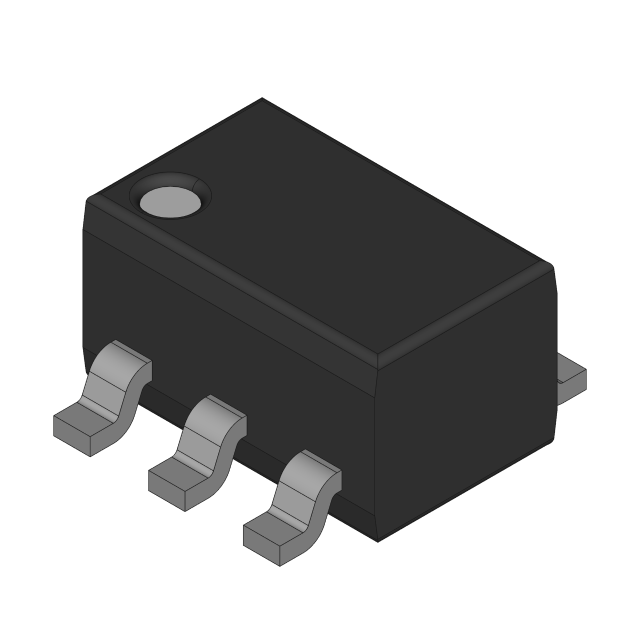
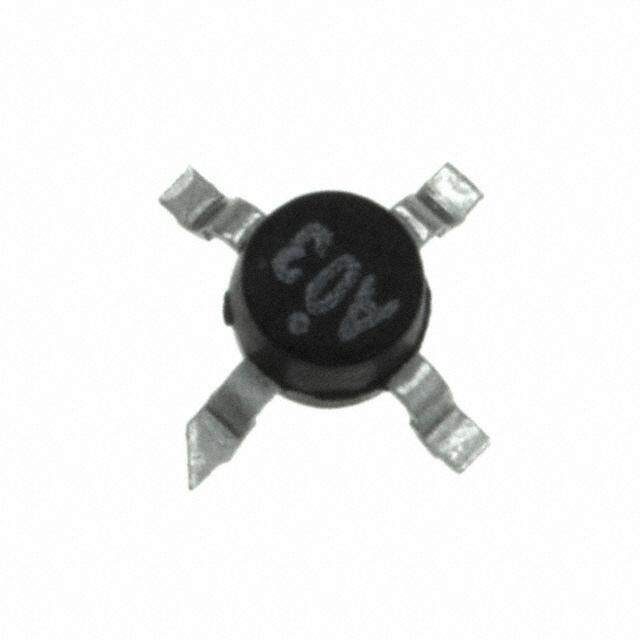
ICGOO电子元器件商城为您提供BGA2869,115由NXP Semiconductors设计生产,在icgoo商城现货销售,并且可以通过原厂、代理商等渠道进行代购。 BGA2869,115价格参考¥2.06-¥2.06。NXP SemiconductorsBGA2869,115封装/规格:RF 放大器, 射频放大器 IC 通用 0Hz ~ 2.2GHz 6-TSSOP。您可以下载BGA2869,115参考资料、Datasheet数据手册功能说明书,资料中有BGA2869,115 详细功能的应用电路图电压和使用方法及教程。
NXP USA Inc. 生产的型号为 BGA2869,115 的 RF 放大器是一款高性能射频功率放大器,广泛应用于无线通信领域。以下是其主要应用场景:

1. 蜂窝通信基站:该放大器适用于 2G、3G 和 4G LTE 基站,提供高线性度和效率,支持多载波操作,满足现代通信系统对带宽和容量的需求。

2. 无线基础设施:可用于小型蜂窝(Small Cell)、微蜂窝和宏蜂窝等无线网络设备中,为信号覆盖和容量扩展提供支持。

3. 点对点无线电通信:在专用微波链路中,BGA2869,115 可用作发射机功率放大器,确保长距离数据传输的可靠性。

4. 雷达系统:适用于气象雷达、空中交通管制雷达和其他需要高功率射频输出的应用场景,提供稳定的信号放大性能。

5. 工业、科学和医疗(ISM)应用:如无线传感器网络、工业自动化设备以及医疗成像系统中的射频模块。

6. 公共安全通信:支持应急服务和公共安全网络中的高可靠性和高效率通信需求。

7. 卫星通信:用于地面终端设备中的射频前端,增强信号传输质量并提高系统效率。

BGA2869,115 的特点包括高增益、宽带宽和低失真,使其成为多种射频应用的理想选择。
| 参数 | 数值 |
| 产品目录 | |
| 描述 | MMIC AMPLIFIER SOT363 |
| 产品分类 | |
| 品牌 | NXP Semiconductors |
| 数据手册 | |
| 产品图片 |
|
| P1dB | 9dBm |
| 产品型号 | BGA2869,115 |
| PCN封装 | |
| RF类型 | 通用 |
| rohs | 无铅 / 符合限制有害物质指令(RoHS)规范要求 |
| 产品系列 | - |
| 供应商器件封装 | 6-TSSOP |
| 其它名称 | 568-8535-1 |
| 包装 | 剪切带 (CT) |
| 噪声系数 | 3.2dB |
| 增益 | 32.2dB |
| 封装/外壳 | 6-TSSOP,SC-88,SOT-363 |
| 标准包装 | 1 |
| 测试频率 | 2.15GHz |
| 电压-电源 | 4.5 V ~ 5.5 V |
| 电流-电源 | 24mA |
| 频率 | 0Hz ~ 2.2GHz |


- 商务部:美国ITC正式对集成电路等产品启动337调查
- 曝三星4nm工艺存在良率问题 高通将骁龙8 Gen1或转产台积电
- 太阳诱电将投资9.5亿元在常州建新厂生产MLCC 预计2023年完工
- 英特尔发布欧洲新工厂建设计划 深化IDM 2.0 战略
- 台积电先进制程称霸业界 有大客户加持明年业绩稳了
- 达到5530亿美元!SIA预计今年全球半导体销售额将创下新高
- 英特尔拟将自动驾驶子公司Mobileye上市 估值或超500亿美元
- 三星加码芯片和SET,合并消费电子和移动部门,撤换高东真等 CEO
- 三星电子宣布重大人事变动 还合并消费电子和移动部门
- 海关总署:前11个月进口集成电路产品价值2.52万亿元 增长14.8%


PDF Datasheet 数据手册内容提取
BGA2869 MMIC wideband amplifier Rev. 3 — 10 July 2015 Product data sheet 1. Product profile 1.1 General description Silicon Monolithic Microwave Integrated Circuit (MMIC) wideband amplifier with internal matching circuit in a 6-pin SOT363 plastic SMD package. 1.2 Features and benefits Internally matched to 50 A gain of 31.7 dB at 950 MHz Output power at 1 dB gain compression = 10 dBm at 950 MHz Supply current = 24.0 mA at a supply voltage of 5.0 V Reverse isolation > 39 dB up to 2150 MHz Good linearity with low second order and third order products Noise figure = 3.1 dB at 950 MHz Unconditionally stable (K > 1) No output inductor required 1.3 Applications LNB IF amplifiers General purpose low noise wideband amplifier for frequencies between DCand2.2GHz 2. Pinning information Table 1. Pinning Pin Description Simplified outline Graphic symbol 1 V CC 6 5 4 1 2, 5 GND2 3 RF_OUT 6 3 4 GND1 4 2, 5 6 RF_IN 1 2 3 sym052
BGA2869 NXP Semiconductors MMIC wideband amplifier 3. Ordering information Table 2. Ordering information Type number Package Name Description Version BGA2869 - plastic surface-mounted package; 6 leads SOT363 4. Marking Table 3. Marking Type number Marking code Description BGA2869 MD* * = - : made in Hong Kong * = p : made in Hong Kong * = W : made in China * = t : made in Malaysia 5. Limiting values Table 4. Limiting values In accordance with the Absolute Maximum Rating System (IEC 60134). Symbol Parameter Conditions Min Max Unit V supply voltage RF input AC coupled 0.5 +7.0 V CC I supply current - 36 mA CC P total power dissipation T = 90 C - 200 mW tot sp T storage temperature 40 +125 C stg T junction temperature - 125 C j P drive power - +10 dBm drive 6. Thermal characteristics Table 5. Thermal characteristics Symbol Parameter Conditions Typ Unit R thermal resistance from junction to P =200mW; T =90C 300 K/W th(j-sp) tot sp solder point 7. Characteristics Table 6. Characterist ics V = 5.0 V; Z = Z = 50 ; P = 34 dBm; T = 25 C; measured on demo board; unless otherwise specified. CC S L i amb Symbol Parameter Conditions Min Typ Max Unit V supply voltage 4.5 5.0 5.5 V CC I supply current 21.8 24.0 26.0 mA CC BGA2869 All information provided in this document is subject to legal disclaimers. © NXP Semiconductors N.V. 2015. All rights reserved. Product data sheet Rev. 3 — 10 July 2015 2 of 13
BGA2869 NXP Semiconductors MMIC wideband amplifier Table 6. Characteristics …continued V = 5.0 V; Z = Z = 50 ; P = 34 dBm; T = 25 C; measured on demo board; unless otherwise specified. CC S L i amb Symbol Parameter Conditions Min Typ Max Unit G power gain f = 250 MHz 30.5 31.1 31.7 dB p f = 950 MHz 31.0 31.7 32.4 dB f = 2150 MHz 30.7 32.2 33.6 dB RL input return loss f = 250 MHz 12 14 16 dB in f = 950 MHz 16 18 20 dB f = 2150 MHz 7 13 20 dB RL output return loss f = 250 MHz 10 15 19 dB out f = 950 MHz 20 21 22 dB f = 2150 MHz 8 10 13 dB ISL isolation f = 250 MHz 41 61 81 dB f = 950 MHz 46 47 49 dB f = 2150 MHz 37 39 42 dB NF noise figure f = 250 MHz 2.6 3.1 3.6 dB f = 950 MHz 2.6 3.1 3.5 dB f = 2150 MHz 2.8 3.2 3.6 dB B 3 dB bandwidth 3 dB below gain at 1GHz 2.8 3.0 3.2 GHz 3dB K Rollett stability factor f = 250 MHz 9 14 19 f = 950 MHz 2 3 4 f = 2150 MHz 1 1 2 P saturated output power f = 250 MHz 12 12 13 dBm L(sat) f = 950 MHz 10 12 13 dBm f = 2150 MHz 9 10 11 dBm P output power at 1 dB gain compression f = 250 MHz 9 10 11 dBm L(1dB) f = 950 MHz 9 10 11 dBm f = 2150 MHz 8 9 10 dBm IP3 input third-order intercept point P =41dBm (for each tone) I drive f =250MHz; f =251MHz 11 9 6 dBm 1 2 f =950MHz; f =951MHz 11 9 7 dBm 1 2 f =2150MHz; f =2151MHz 16 13 10 dBm 1 2 IP3 output third-order intercept point P =41dBm (for each tone) O drive f =250MHz; f =251MHz 20 23 25 dBm 1 2 f =950MHz; f =951MHz 20 23 25 dBm 1 2 f =2150MHz; f =2151MHz 16 19 22 dBm 1 2 P second harmonic output power P =38dBm L(2H) drive f =250MHz; f =500MHz 69 67 65 dBm 1H 2H f =950MHz; f =1900MHz 53 51 49 dBm 1H 2H IM2 second-order intermodulation distance P =38dBm (for each tone) drive f =250MHz; f =251MHz 40 42 44 dBc 1 2 f =950MHz; f =951MHz 34 36 38 dBc 1 2 BGA2869 All information provided in this document is subject to legal disclaimers. © NXP Semiconductors N.V. 2015. All rights reserved. Product data sheet Rev. 3 — 10 July 2015 3 of 13
BGA2869 NXP Semiconductors MMIC wideband amplifier 8. Application information Figure1 shows a typical application circuit for the BGA2869 MMIC. The device is internally matched to 50 , and therefore does not need any external matching. The value of the input and output DC blocking capacitors C1 and C2 should not be more than 470 pF for applications above 100 MHz. However, when the device is operated below 100 MHz, the capacitor value should be increased. The location of the 470 pF supply decoupling capacitor (C ) can be precisely chosen for dec optimum performance. The PCB top ground plane, connected to pins 2, 4 and 5 must be as close as possible to the MMIC, preferably also below the MMIC. When using via holes, use multiple via holes as close as possible to the MMIC. (cid:57)(cid:54) (cid:38)(cid:71)(cid:72)(cid:70) (cid:57)(cid:54) (cid:38)(cid:20) (cid:53)(cid:41)(cid:66)(cid:44)(cid:49) (cid:53)(cid:41)(cid:66)(cid:50)(cid:56)(cid:55) (cid:38)(cid:21) (cid:53)(cid:41)(cid:3)(cid:76)(cid:81)(cid:83)(cid:88)(cid:87) (cid:53)(cid:41)(cid:3)(cid:82)(cid:88)(cid:87)(cid:83)(cid:88)(cid:87) (cid:42)(cid:49)(cid:39)(cid:20) (cid:42)(cid:49)(cid:39)(cid:21) (cid:68)(cid:68)(cid:68)(cid:16)(cid:19)(cid:19)(cid:22)(cid:26)(cid:24)(cid:26) Fig 1. Typical application circuit 8.1 Application examples wideband wideband mixer amplifier LNA amplifier mixer from RF to IF circuit antenna to IF circuit circuit or demodulator or demodulator oscillator oscillator 001aaf762 001aaf763 The MMIC is very suitable as IF amplifier in e.g. LNB’s. As second amplifier after an LNA, the MMIC offers an The excellent wideband characteristics make it an easy easy matching, low noise solution. building block. Fig 2. Application as IF amplifier Fig 3. Application as RF amplifier 8.2 Tables Table 7. Supply current over temperature and supply voltages Typical values. Symbol Parameter Conditions T (C) Unit amb 40 +25 +85 I supply current V =4.5V 23.60 21.80 20.30 mA CC CC V =5.0V 25.80 24.00 22.40 mA CC V =5.5V 27.80 26.00 24.50 mA CC BGA2869 All information provided in this document is subject to legal disclaimers. © NXP Semiconductors N.V. 2015. All rights reserved. Product data sheet Rev. 3 — 10 July 2015 4 of 13
BGA2869 NXP Semiconductors MMIC wideband amplifier Table 8. Second harmonic output power over temperature and supply voltages Typical values. Symbol Parameter Conditions T (C) Unit amb 40 +25 +85 P second harmonic output power f = 250 MHz; P =38dBm L(2H) drive V =4.5 V 58 67 68 dBm CC V =5.0V 72 67 61 dBm CC V =5.5V 64 60 58 dBm CC f = 950 MHz; P =38dBm drive V =4.5 V 69 55 50 dBm CC V =5.0V 55 51 48 dBm CC V =5.5V 51 49 46 dBm CC Table 9. Input power at 1 dB gain compression over temperature and supply voltages Typical values. Symbol Parameter Conditions T (C) Unit amb 40 +25 +85 P input power at 1dB gain compression f = 250 MHz i(1dB) V =4.5 V 21 21 21 dBm CC V =5.0V 20 20 20 dBm CC V =5.5V 19 20 20 dBm CC f = 950 MHz V =4.5 V 21 21 21 dBm CC V =5.0V 21 21 21 dBm CC V =5.5V 20 20 20 dBm CC f = 2150 MHz V =4.5 V 22 22 23 dBm CC V =5.0V 21 22 23 dBm CC V =5.5V 21 22 24 dBm CC BGA2869 All information provided in this document is subject to legal disclaimers. © NXP Semiconductors N.V. 2015. All rights reserved. Product data sheet Rev. 3 — 10 July 2015 5 of 13
BGA2869 NXP Semiconductors MMIC wideband amplifier Table 10. Output power at 1 dB gain compression over temperature and supply voltages Typical values. Symbol Parameter Conditions T (C) Unit amb 40 +25 +85 P output power at 1dB gain compression f = 250 MHz L(1dB) V =4.5 V 9 9 8 dBm CC V =5.0V 11 10 10 dBm CC V =5.5V 12 11 11 dBm CC f = 950 MHz V =4.5 V 9 8 8 dBm CC V =5.0V 10 10 9 dBm CC V =5.5V 11 11 10 dBm CC f = 2150 MHz V =4.5 V 9 8 6 dBm CC V =5.0V 10 9 7 dBm CC V =5.5V 11 9 7 dBm CC Table 11. Saturated output power over temperature and supply voltages Typical values. Symbol Parameter Conditions T (C) Unit amb 40 +25 +85 P saturated output power f = 250 MHz L(sat) V =4.5 V 11 11 10 dBm CC V =5.0V 13 12 12 dBm CC V =5.5V 14 13 13 dBm CC f = 950 MHz V =4.5 V 11 11 11 dBm CC V =5.0V 12 12 12 dBm CC V =5.5V 14 13 13 dBm CC f = 2150 MHz V =4.5 V 10 9 8 dBm CC V =5.0V 11 10 8 dBm CC V =5.5V 12 10 9 dBm CC BGA2869 All information provided in this document is subject to legal disclaimers. © NXP Semiconductors N.V. 2015. All rights reserved. Product data sheet Rev. 3 — 10 July 2015 6 of 13
BGA2869 NXP Semiconductors MMIC wideband amplifier Table 12. Second-order intermodulation distance over temperature and supply voltages Typical values. Symbol Parameter Conditions T (C) Unit amb 40 +25 +85 IM2 second-order intermodulation distance f =250MHz; 1 f =251MHz; 2 P =38dBm drive V =4.5 V 36 39 42 dBc CC V =5.0V 40 42 45 dBc CC V =5.5V 43 45 48 dBc CC f =950MHz; 1 f =951MHz; 2 P =38 dBm drive V =4.5 V 33 34 36 dBc CC V =5.0V 35 36 37 dBc CC V =5.5V 37 37 37 dBc CC Table 13. Output third-order intercept point over temperature and supply voltages Typical values. Symbol Parameter Conditions T (C) Unit amb 40 +25 +85 IP3 output third-order intercept point f =250MHz; O 1 f =251MHz; 2 P =41dBm drive V =4.5 V 21 21 20 dBm CC V =5.0V 23 23 22 dBm CC V =5.5V 25 25 24 dBm CC f =950MHz; 1 f =951MHz; 2 P =41dBm drive V =4.5 V 21 21 20 dBm CC V =5.0V 23 23 22 dBm CC V =5.5V 25 24 23 dBm CC f =2150MHz; 1 f =2151MHz; 2 P =41dBm drive V =4.5 V 21 19 17 dBm CC V =5.0V 22 19 17 dBm CC V =5.5V 22 20 17 dBm CC T able 14. 3 dB bandwidth over temperature and supply voltages Typical values. Symbol Parameter Conditions T (C) Unit amb 40 +25 +85 B 3 dB bandwidth V =4.5V 3.15 2.98 2.80 GHz 3dB CC V =5.0V 3.14 2.96 2.79 GHz CC V =5.5V 3.12 2.95 2.77 GHz CC BGA2869 All information provided in this document is subject to legal disclaimers. © NXP Semiconductors N.V. 2015. All rights reserved. Product data sheet Rev. 3 — 10 July 2015 7 of 13
BGA2869 NXP Semiconductors MMIC wideband amplifier 9. Test information (cid:37)(cid:42)(cid:36)(cid:21)(cid:91)(cid:91)(cid:91)(cid:3)(cid:54)(cid:50)(cid:55)(cid:22)(cid:25)(cid:22)(cid:3)(cid:40)(cid:57)(cid:37) (cid:53)(cid:54) (cid:56)(cid:55) (cid:50) (cid:50) (cid:38)(cid:55) (cid:53)(cid:41) (cid:56) (cid:39) (cid:49) (cid:50) (cid:42)(cid:49)(cid:39) (cid:48)(cid:44)(cid:38) (cid:38)(cid:21) (cid:51)(cid:24)(cid:51)(cid:25)(cid:51)(cid:26)(cid:51)(cid:27)(cid:51)(cid:28)(cid:51)(cid:20)(cid:19)(cid:51)(cid:20)(cid:20)(cid:51)(cid:20)(cid:21)(cid:51)(cid:20)(cid:22) (cid:40) (cid:54) (cid:20) (cid:57)(cid:38)(cid:38) (cid:23)(cid:24)(cid:25)(cid:26)(cid:27)(cid:28)(cid:19)(cid:20)(cid:21)(cid:22)(cid:23) (cid:20)(cid:20)(cid:20)(cid:20)(cid:20)(cid:20)(cid:21)(cid:21)(cid:21)(cid:21)(cid:21) (cid:51)(cid:51)(cid:51)(cid:51)(cid:51)(cid:51)(cid:51)(cid:51)(cid:51)(cid:51)(cid:51) (cid:42)(cid:49)(cid:39) (cid:38)(cid:20) (cid:49) (cid:41)(cid:44) (cid:53) (cid:68)(cid:68)(cid:68)(cid:16)(cid:19)(cid:19)(cid:23)(cid:22)(cid:22)(cid:26) For decoupling a decoupling capacitor (Cdec) is used on one of the positions of P5 to P24. The results mentioned in this data sheet have been obtained using the decoupling capacitor Cdec on position P22. The distance between the center of pin 1 and the center of position P22 is 7.43 mm. Fig 4. PCB layout and demo board with components T able 15. List of components used for the typical application Component Description Value Dimensions Remarks C1, C2 multilayer ceramic chip 470 pF 0603 X7R RF coupling capacitor capacitor P5 to P24 [1] position for multilayer 470 pF 0603 X7R RF decoupling capacitor ceramic chip capacitor C dec IC1 BGA2869 MMIC - SOT363 [1] For decoupling a decoupling capacitor (C ) is used on one of the positions of P5 to P24. The results dec mentioned in this data sheet have been obtained using the decoupling capacitor Cdec on position P22. BGA2869 All information provided in this document is subject to legal disclaimers. © NXP Semiconductors N.V. 2015. All rights reserved. Product data sheet Rev. 3 — 10 July 2015 8 of 13
BGA2869 NXP Semiconductors MMIC wideband amplifier 10. Package outline Plastic surface-mounted package; 6 leads SOT363 D B E A X y HE v M A 6 5 4 Q pin 1 index A A1 1 2 3 c e1 bp w M B Lp e detail X 0 1 2 mm scale DIMENSIONS (mm are the original dimensions) A1 UNIT A max bp c D E e e1 HE Lp Q v w y 1.1 0.30 0.25 2.2 1.35 2.2 0.45 0.25 mm 0.1 1.3 0.65 0.2 0.2 0.1 0.8 0.20 0.10 1.8 1.15 2.0 0.15 0.15 OUTLINE REFERENCES EUROPEAN ISSUE DATE VERSION IEC JEDEC JEITA PROJECTION 04-11-08 SOT363 SC-88 06-03-16 Fig 5. Package outline SOT363 BGA2869 All information provided in this document is subject to legal disclaimers. © NXP Semiconductors N.V. 2015. All rights reserved. Product data sheet Rev. 3 — 10 July 2015 9 of 13
BGA2869 NXP Semiconductors MMIC wideband amplifier 11. Abbreviations Table 16. Abbreviations Acronym Description IF Intermediate Frequency LNA Low-Noise Amplifier LNB Low-Noise Block converter PCB Printed-Circuit Board SMD Surface Mounted Device 12. Revision history Table 17. Revision history Document ID Release date Data sheet status Change notice Supersedes BGA2869 v.3 20150710 Product data sheet - BGA2869 v.2 Modifications: • The format of this data sheet has been redesigned to comply with the new identity guidelines of NXP Semiconductors. • Legal texts have been adapted to the new company name where appropriate. BGA2869 v.2 20130826 Product data sheet - BGA2869 v.1 BGA2869 v.1 20120717 Product data sheet - - BGA2869 All information provided in this document is subject to legal disclaimers. © NXP Semiconductors N.V. 2015. All rights reserved. Product data sheet Rev. 3 — 10 July 2015 10 of 13
BGA2869 NXP Semiconductors MMIC wideband amplifier 13. Legal information 13.1 Data sheet status Document status[1][2] Product status[3] Definition Objective [short] data sheet Development This document contains data from the objective specification for product development. Preliminary [short] data sheet Qualification This document contains data from the preliminary specification. Product [short] data sheet Production This document contains the product specification. [1] Please consult the most recently issued document before initiating or completing a design. [2] The term ‘short data sheet’ is explained in section “Definitions”. [3] The product status of device(s) described in this document may have changed since this document was published and may differ in case of multiple devices. The latest product status information is available on the Internet at URLhttp://www.nxp.com. 13.2 Definitions Suitability for use — NXP Semiconductors products are not designed, authorized or warranted to be suitable for use in life support, life-critical or safety-critical systems or equipment, nor in applications where failure or Draft — The document is a draft version only. The content is still under malfunction of an NXP Semiconductors product can reasonably be expected internal review and subject to formal approval, which may result in to result in personal injury, death or severe property or environmental modifications or additions. NXP Semiconductors does not give any damage. NXP Semiconductors and its suppliers accept no liability for representations or warranties as to the accuracy or completeness of inclusion and/or use of NXP Semiconductors products in such equipment or information included herein and shall have no liability for the consequences of applications and therefore such inclusion and/or use is at the customer’s own use of such information. risk. Short data sheet — A short data sheet is an extract from a full data sheet Applications — Applications that are described herein for any of these with the same product type number(s) and title. A short data sheet is intended products are for illustrative purposes only. NXP Semiconductors makes no for quick reference only and should not be relied upon to contain detailed and representation or warranty that such applications will be suitable for the full information. For detailed and full information see the relevant full data specified use without further testing or modification. sheet, which is available on request via the local NXP Semiconductors sales office. In case of any inconsistency or conflict with the short data sheet, the Customers are responsible for the design and operation of their applications full data sheet shall prevail. and products using NXP Semiconductors products, and NXP Semiconductors accepts no liability for any assistance with applications or customer product Product specification — The information and data provided in a Product design. It is customer’s sole responsibility to determine whether the NXP data sheet shall define the specification of the product as agreed between Semiconductors product is suitable and fit for the customer’s applications and NXP Semiconductors and its customer, unless NXP Semiconductors and products planned, as well as for the planned application and use of customer have explicitly agreed otherwise in writing. In no event however, customer’s third party customer(s). Customers should provide appropriate shall an agreement be valid in which the NXP Semiconductors product is design and operating safeguards to minimize the risks associated with their deemed to offer functions and qualities beyond those described in the applications and products. Product data sheet. NXP Semiconductors does not accept any liability related to any default, damage, costs or problem which is based on any weakness or default in the 13.3 Disclaimers customer’s applications or products, or the application or use by customer’s third party customer(s). Customer is responsible for doing all necessary testing for the customer’s applications and products using NXP Limited warranty and liability — Information in this document is believed to Semiconductors products in order to avoid a default of the applications and be accurate and reliable. However, NXP Semiconductors does not give any the products or of the application or use by customer’s third party representations or warranties, expressed or implied, as to the accuracy or customer(s). NXP does not accept any liability in this respect. completeness of such information and shall have no liability for the consequences of use of such information. NXP Semiconductors takes no Limiting values — Stress above one or more limiting values (as defined in responsibility for the content in this document if provided by an information the Absolute Maximum Ratings System of IEC60134) will cause permanent source outside of NXP Semiconductors. damage to the device. Limiting values are stress ratings only and (proper) operation of the device at these or any other conditions above those given in In no event shall NXP Semiconductors be liable for any indirect, incidental, the Recommended operating conditions section (if present) or the punitive, special or consequential damages (including - without limitation - lost Characteristics sections of this document is not warranted. Constant or profits, lost savings, business interruption, costs related to the removal or repeated exposure to limiting values will permanently and irreversibly affect replacement of any products or rework charges) whether or not such the quality and reliability of the device. damages are based on tort (including negligence), warranty, breach of contract or any other legal theory. Terms and conditions of commercial sale — NXP Semiconductors products are sold subject to the general terms and conditions of commercial Notwithstanding any damages that customer might incur for any reason whatsoever, NXP Semiconductors’ aggregate and cumulative liability towards sale, as published at http://www.nxp.com/profile/terms, unless otherwise customer for the products described herein shall be limited in accordance agreed in a valid written individual agreement. In case an individual with the Terms and conditions of commercial sale of NXP Semiconductors. agreement is concluded only the terms and conditions of the respective agreement shall apply. NXP Semiconductors hereby expressly objects to Right to make changes — NXP Semiconductors reserves the right to make applying the customer’s general terms and conditions with regard to the changes to information published in this document, including without purchase of NXP Semiconductors products by customer. limitation specifications and product descriptions, at any time and without notice. This document supersedes and replaces all information supplied prior No offer to sell or license — Nothing in this document may be interpreted or to the publication hereof. construed as an offer to sell products that is open for acceptance or the grant, conveyance or implication of any license under any copyrights, patents or other industrial or intellectual property rights. BGA2869 All information provided in this document is subject to legal disclaimers. © NXP Semiconductors N.V. 2015. All rights reserved. Product data sheet Rev. 3 — 10 July 2015 11 of 13
BGA2869 NXP Semiconductors MMIC wideband amplifier Export control — This document as well as the item(s) described herein NXP Semiconductors’ specifications such use shall be solely at customer’s may be subject to export control regulations. Export might require a prior own risk, and (c) customer fully indemnifies NXP Semiconductors for any authorization from competent authorities. liability, damages or failed product claims resulting from customer design and use of the product for automotive applications beyond NXP Semiconductors’ Non-automotive qualified products — Unless this data sheet expressly standard warranty and NXP Semiconductors’ product specifications. states that this specific NXP Semiconductors product is automotive qualified, the product is not suitable for automotive use. It is neither qualified nor tested Translations — A non-English (translated) version of a document is for in accordance with automotive testing or application requirements. NXP reference only. The English version shall prevail in case of any discrepancy Semiconductors accepts no liability for inclusion and/or use of between the translated and English versions. non-automotive qualified products in automotive equipment or applications. In the event that customer uses the product for design-in and use in 13.4 Trademarks automotive applications to automotive specifications and standards, customer (a) shall use the product without NXP Semiconductors’ warranty of the Notice: All referenced brands, product names, service names and trademarks product for such automotive applications, use and specifications, and (b) are the property of their respective owners. whenever customer uses the product for automotive applications beyond 14. Contact information For more information, please visit: http://www.nxp.com For sales office addresses, please send an email to: salesaddresses@nxp.com BGA2869 All information provided in this document is subject to legal disclaimers. © NXP Semiconductors N.V. 2015. All rights reserved. Product data sheet Rev. 3 — 10 July 2015 12 of 13
BGA2869 NXP Semiconductors MMIC wideband amplifier 15. Contents 1 Product profile. . . . . . . . . . . . . . . . . . . . . . . . . . 1 1.1 General description . . . . . . . . . . . . . . . . . . . . . 1 1.2 Features and benefits. . . . . . . . . . . . . . . . . . . . 1 1.3 Applications . . . . . . . . . . . . . . . . . . . . . . . . . . . 1 2 Pinning information. . . . . . . . . . . . . . . . . . . . . . 1 3 Ordering information. . . . . . . . . . . . . . . . . . . . . 2 4 Marking. . . . . . . . . . . . . . . . . . . . . . . . . . . . . . . . 2 5 Limiting values. . . . . . . . . . . . . . . . . . . . . . . . . . 2 6 Thermal characteristics . . . . . . . . . . . . . . . . . . 2 7 Characteristics. . . . . . . . . . . . . . . . . . . . . . . . . . 2 8 Application information. . . . . . . . . . . . . . . . . . . 4 8.1 Application examples . . . . . . . . . . . . . . . . . . . . 4 8.2 Tables. . . . . . . . . . . . . . . . . . . . . . . . . . . . . . . . 4 9 Test information. . . . . . . . . . . . . . . . . . . . . . . . . 8 10 Package outline. . . . . . . . . . . . . . . . . . . . . . . . . 9 11 Abbreviations. . . . . . . . . . . . . . . . . . . . . . . . . . 10 12 Revision history. . . . . . . . . . . . . . . . . . . . . . . . 10 13 Legal information. . . . . . . . . . . . . . . . . . . . . . . 11 13.1 Data sheet status . . . . . . . . . . . . . . . . . . . . . . 11 13.2 Definitions. . . . . . . . . . . . . . . . . . . . . . . . . . . . 11 13.3 Disclaimers. . . . . . . . . . . . . . . . . . . . . . . . . . . 11 13.4 Trademarks. . . . . . . . . . . . . . . . . . . . . . . . . . . 12 14 Contact information. . . . . . . . . . . . . . . . . . . . . 12 15 Contents. . . . . . . . . . . . . . . . . . . . . . . . . . . . . . 13 Please be aware that important notices concerning this document and the product(s) described herein, have been included in section ‘Legal information’. © NXP Semiconductors N.V. 2015. All rights reserved. For more information, please visit: http://www.nxp.com For sales office addresses, please send an email to: salesaddresses@nxp.com Date of release: 10 July 2015 Document identifier: BGA2869
Mouser Electronics Authorized Distributor Click to View Pricing, Inventory, Delivery & Lifecycle Information: N XP: BGA2869,115