ICGOO在线商城 > BD9327EFJ-E2
 Datasheet下载
- 型号: BD9327EFJ-E2
- 制造商: ROHM Semiconductor
- 库位|库存: xxxx|xxxx
- 要求:
| 数量阶梯 | 香港交货 | 国内含税 |
| +xxxx | $xxxx | ¥xxxx |
查看当月历史价格
查看今年历史价格
BD9327EFJ-E2产品简介:
ICGOO电子元器件商城为您提供BD9327EFJ-E2由ROHM Semiconductor设计生产,在icgoo商城现货销售,并且可以通过原厂、代理商等渠道进行代购。 提供BD9327EFJ-E2价格参考¥27.08-¥33.26以及ROHM SemiconductorBD9327EFJ-E2封装/规格参数等产品信息。 你可以下载BD9327EFJ-E2参考资料、Datasheet数据手册功能说明书, 资料中有BD9327EFJ-E2详细功能的应用电路图电压和使用方法及教程。
| 参数 | 数值 |
| 产品目录 | 集成电路 (IC) |
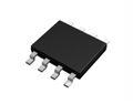
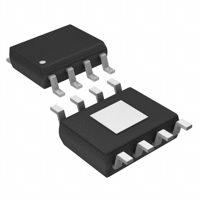
| 描述 | IC REG BUCK SYNC ADJ 4A 8TSOP |
| 产品分类 | |
| 品牌 | Rohm Semiconductor |
| 数据手册 | |
| 产品图片 |
|
| 产品型号 | BD9327EFJ-E2 |
| PWM类型 | 电流模式 |
| rohs | 无铅 / 符合限制有害物质指令(RoHS)规范要求 |
| 产品系列 | - |
| 供应商器件封装 | 8-TSOP |
| 其它名称 | BD9327EFJ-E2TR |
| 包装 | 带卷 (TR) |
| 同步整流器 | 是 |
| 安装类型 | 表面贴装 |
| 封装/外壳 | 8-SOIC(0.154",3.90mm 宽)裸焊盘 |
| 工作温度 | -40°C ~ 85°C |
| 标准包装 | 2,500 |
| 电压-输入 | 4.75 V ~ 18 V |
| 电压-输出 | 0.9 V ~ 14.4 V |
| 电流-输出 | 4A |
| 类型 | 降压(降压) |
| 输出数 | 1 |
| 输出类型 | 可调式 |
| 频率-开关 | 380kHz |


- 商务部:美国ITC正式对集成电路等产品启动337调查
- 曝三星4nm工艺存在良率问题 高通将骁龙8 Gen1或转产台积电
- 太阳诱电将投资9.5亿元在常州建新厂生产MLCC 预计2023年完工
- 英特尔发布欧洲新工厂建设计划 深化IDM 2.0 战略
- 台积电先进制程称霸业界 有大客户加持明年业绩稳了
- 达到5530亿美元!SIA预计今年全球半导体销售额将创下新高
- 英特尔拟将自动驾驶子公司Mobileye上市 估值或超500亿美元
- 三星加码芯片和SET,合并消费电子和移动部门,撤换高东真等 CEO
- 三星电子宣布重大人事变动 还合并消费电子和移动部门
- 海关总署:前11个月进口集成电路产品价值2.52万亿元 增长14.8%


PDF Datasheet 数据手册内容提取
Datasheet 4.75V to 18V, 2A/3A/4A 1ch Buck Converter with In tegrated FET BD9325FJ BD9326EFJ BD9327EFJ General Description Key Specifications The BD9325FJ, BD9326EFJ and BD9327EFJ are Input Voltage Range: 4.75V to 18V step-down regulators with built-in low resistance high Output Current side N-Channel MOSFET. These ICs can supply BD9327EFJ : 4.0A (Max) continuous output current of 2A / 3A / 4A BD9326EFJ: 3.0A (Max) respectively over a wide input range, and provides BD9325FJ: 2.0A (Max) not only fast transient response, but also easy phase Switching Frequency: 380kHz (Typ) compensation because of current mode control. High Side FET ON-Resistance BD9327EFJ: 0.11Ω(Typ) Features BD9326EFJ: 0.12Ω(Typ) Low ESR Output Ceramic Capacitors are Available BD9325FJ: 0.16Ω(Typ) Low Standby Current during Shutdown Mode Low Side FET ON-Resistance: 10Ω(Typ) Feedback Voltage Standby Current: 80μA (Typ) 0.9V ± 1.5%(Ta=25°C) Operating Temperature Range: -40°C to +85°C 0.9V ± 3.0%(Ta=-25°C to +85°C) Protection Circuit: Packages W(Typ) D(Typ) H(Max) Under Voltage Protection Thermal Shutdown Over-Current Protection Applications Distributed Power System Pre-Regulator for Linear Regulator HTSOP-J8 4.90mm x 6.00mm x 1.00mm SOP-J8 4.90mm x 6.00mm x 1.65mm Typical Application Circuit C_PC1 3300pF R_DW C_SS R_PC 10k 15k 0.1μF P R_UP SS EN COM FB 27k Thermal Pad (For BD9326EFJ, BD9327EFJ) BST VIN SW GND L VIN=12V VOUT = 3.3V 10μH C_VC1 D C_CO1 10μF S F 20μF Bμ _1 C0. Figure 1. Typical Application Circuit 〇Product structure : Silicon monolithic integrated circuit 〇This product has no designed protection against radioactive rays .w ww.rohm.com TSZ02201-0323AAJ00030-1-2 © 2012 ROHM Co., Ltd. All rights reserved. 1/19 TSZ22111 • 14 • 001 05.Sep.2014 Rev.002
BD9325FJ BD9326EFJ BD9327EFJ Pin Configuration Block Diagram VIN (TOP VIEW) 1 BST SS 8 2 VIN EN 7 3 SW COMP 6 4 GND FB 5 Figure 2. Pin Configuration Figure 3. Block Diagram Pin Description Pin No. Pin Name Function 1 BST High-side gate drive boost input 2 VIN Power supply input terminal 3 SW Power switching output 4 GND Ground terminal 5 FB Feedback input 6 COMP Compensation node 7 EN Enable input 8 SS Soft start control input Lineup High Side FET Output Current Orderable ON-Resistance Package (Max) Part Number (Typ) 0.16 Ω 2.0 A SOP-J8 Reel of 2500 BD9325FJ-E2 0.12 Ω 3.0 A HTSOP-J8 Reel of 2500 BD9326EFJ-E2 0.11 Ω 4.0 A HTSOP-J8 Reel of 2500 BD9327EFJ-E2 www.rohm.com TSZ02201-0323AAJ00030-1-2 © 2012 ROHM Co., Ltd. All rights reserved. 2/19 TSZ22111・15・001 05.Sep.2014 Rev.002
BD9325FJ BD9326EFJ BD9327EFJ Absolute Maximum Ratings (Ta = 25°C) Parameter Symbol Rating Unit Supply Voltage [VIN] VIN 20 V Switch Voltage [SW] VSW 20 V Power Dissipation for HTSOP-J8 Pd1 3.76 (Note 1) W Power Dissipation for SOP-J8 Pd2 0.67 (Note 2) W Operating Temperature Range Topr -40 to +85 °C Storage Temperature Range Tstg -55 to +150 °C Maximum Junction Temperature Tjmax 150 °C BST Voltage VBST VSW+7 V EN Voltage VEN 20 V All Other Pins VOTH 7 V (Note 1) Mounted on 4- layer 70mmx70mmx1.6mm board. Reduce by 30.08mW/°C for Ta above 25°C. (Note 2) Mounted on 1- layer 70mmx70mmx1.6mm board. Reduce by 5.4mW/°C for Ta above 25°C. Caution: Operating the IC over the absolute maximum ratings may damage the IC. The damage can either be a short circuit between pins or an open circuit between pins and the internal circuitry. Therefore, it is important to consider circuit protection measures, such as adding a fuse, in case the IC is operated over the absolute maximum ratings. Recommended Operating Conditions (Ta= -40°C to +85°C) Rating Parameter Symbol Unit Min Typ Max Supply Voltage VIN 4.75 12 18 V SW Voltage VSW -0.5 - +18 V Output Current for BD9325FJ ISW2 - - 2(Note 3) A Output Current for BD9326EFJ ISW3 - - 3(Note 3) A Output Current for BD9327EFJ ISW4 - - 4(Note 3) A (Note 3) Pd, ASO should not be exceeded Electrical Characteristics (Unless otherwise specified VIN=12V Ta=25°C) Limit Parameter Symbol Unit Conditions Min Typ Max Error Amplifier Block FB Input Bias Current IFB - 0.1 2 µA Feedback Voltage1 VFB1 0.886 0.900 0.914 V Voltage Follower Feedback Voltage2 VFB2 0.873 0.900 0.927 V Ta=-40°C to +85°C SW Block – SW Hi-Side FET ON-Resistance for BD9325FJ RON2 - 0.16 - Ω ISW= -0.8A (Note 4) Hi-Side FET ON-Resistance for BD9326EFJ RON3 - 0.12 - Ω ISW= -0.8A (Note 4) Hi-Side FET ON-Resistance for BD9327EFJ RON4 - 0.11 - Ω ISW= -0.8A (Note 4) Low-Side FET ON-Resistance RONL - 10 - Ω ISW= 0.1A Leak Current N-Channel ILEAKN - 0 10 µA VIN= 18V, VSW= 0V Switch Current Limit for BD9325FJ ILIMIT2 2.5 - - A (Note 4) Switch Current Limit for BD9326EFJ ILIMIT3 3.5 - - A (Note 4) Switch Current Limit for BD9327EFJ ILIMIT4 4.5 - - A (Note 4) Maximum Duty Cycle MDUTY - 90 - % VFB= 0V General Enable Sink Current IEN 86 181 275 µA VEN= 12V Enable Threshold Voltage VEN 1.1 1.18 1.4 V Under Voltage Lockout Threshold VUVLO 4.05 4.40 4.75 V VIN Rising Under Voltage Lockout Hysteresis VHYS - 0.1 - V Soft Start Current ISS 23 41 62 µA VSS= 0 V Soft Start Time tSS - 1.6 - ms CSS= 0.1 µF Operating Frequency fOSC 300 380 460 kHz Circuit Current ICC - 2.1 4.3 mA VFB= 1.5V, VEN= 12V Standby Current IQUI - 80 170 µA VEN= 0V (Note 4) See the lineup table . www.rohm.com TSZ02201-0323AAJ00030-1-2 © 2012 ROHM Co., Ltd. All rights reserved. 3/19 TSZ22111・15・001 05.Sep.2014 Rev.002
BD9325FJ BD9326EFJ BD9327EFJ Typical Performance Curves (Unless otherwise specified, VIN= 12V Ta = 25°C) mA] A] cc :[ c :[μ I c I VIN :[V] VIN :[V] Figure 4. Circuit Current vs Input Voltage Figure 5. Standby Current vs Input Voltage (No Switching) (IC Not Active) V] :[ A] ge a μ t :[ ol B V IF k c a b d e e F VFB :[V] Temperature :[ °C ] Figure 6. Input Bias Current vs Figure 7. Feedback Voltage vs Feedback Voltage Temperature www.rohm.com TSZ02201-0323AAJ00030-1-2 © 2012 ROHM Co., Ltd. All rights reserved. 4/19 TSZ22111・15・001 05.Sep.2014 Rev.002
BD9325FJ BD9326EFJ BD9327EFJ Typical Performance Curves - continued 390 380 Hz] 370 k Ω] ncy [ 360 :[ ue R ON Freq 350 g n erati 340 p O 330 320 -40 -20 0 20 40 60 80 Ta: [°C] TTEeMmPpEeRraAtuTrUeR :E[ ° :C [ C] ] Figure 8. Hi-Side ON-Resistance Figure 9. Operating Frequency vs vs Temperature Temperature s] m %] e :[ [ m ncy : art Ti Efficie Soft St CSS: [μF] IOUT: [A] Figure 10. Efficiency vs Output Current Figure 11. Soft Start Time vs (VIN= 12V VOUT= 3.3V L=10µH) Soft Start Capacitor www.rohm.com TSZ02201-0323AAJ00030-1-2 © 2012 ROHM Co., Ltd. All rights reserved. 5/19 TSZ22111・15・001 05.Sep.2014 Rev.002
BD9325FJ BD9326EFJ BD9327EFJ Typical Waveforms Figure 12. Over-Current Protection Figure 13. Transient Response (VOUT is shorted to GND) (VIN= 12V VOUT= 3.3V L= 10µH COUT =22µF IOUT= 0.2-1.0A ) Figure 14. Output Ripple Voltage Figure 15. Transient Response (VIN= 12V VOUT= 3.3V L= 10µH COUT =22µF IOUT= 1.0A ) (VIN= 12V VOUT= 3.3V L= 10µH COUT =22µF IOUT= 0.2-3.0A) www.rohm.com TSZ02201-0323AAJ00030-1-2 © 2012 ROHM Co., Ltd. All rights reserved. 6/19 TSZ22111・15・001 05.Sep.2014 Rev.002
BD9325FJ BD9326EFJ BD9327EFJ Typical Waveforms - continued Figure 16. Output Ripple Voltage Figure 17. Start Up Waveform (VIN= 12V VOUT= 3.3V L= 10µH COUT =22µF IOUT= 3.0A) (VIN= 12V VOUT= 3.3V L= 22µH CSS= 0.1µF IOUT= 0A) www.rohm.com TSZ02201-0323AAJ00030-1-2 © 2012 ROHM Co., Ltd. All rights reserved. 7/19 TSZ22111・15・001 05.Sep.2014 Rev.002
BD9325FJ BD9326EFJ BD9327EFJ Application Information 1. Block Operation (1) VREG This block generates the constant-voltage needed for DC/DC boosting. (2) VREF This block generates the 2.9 V internal reference voltage of the Error Amp. (3) TSD/UVLO TSD (Thermal shutdown)/UVLO (Under Voltage Lockout) are protection circuit blocks. This circuit protects the device from damages due to excessive heat and power dissipation. When the TSD circuit is triggered by temperature exceeding the 175°C Maximum Junction Temperature, it shuts down the device. Once temperature falls below the threshold set by a hysteresis, the device resumes operation. UVLO circuit prevents error in the device operation due to either excessive or insufficient power supply voltage. It monitors the voltage level at VIN pin and also the output of REG block. Once VIN voltage falls below 4.4V, the UVLO circuit disables the device and resets the Soft-Start circuit. Typical UVLO Hysteresis is 100 mV. (4) Error Amp Block (ERR) This circuit compares the reference voltage and the feedback of output voltage. The COMP pin voltage, which is the output of ERR block, determines the switching duty. During startup, the COMP pin voltage is limited by SS pin voltage since the soft start is operated by the SS pin voltage. (5) Oscillator Block (OSC) This block generates the internal oscillating frequency of the IC. (6) SLOPE Block This circuit is used to generate triangular waveform from the clock created by OSC block. This triangular waveform is sent to the PWM comparator. (7) PWM Block The COMP pin voltage, which is the output of ERR block, is compared to the SLOPE block's triangular waveform to determine the switching duty. Since the switching duty is limited by the maximum duty ratio which is determined internally, it does not become 100%. (8) DRV Block This circuit is a DC/DC driver block. A signal from the PWM serves as the input to drive the power FETs. (9) OCP Block OCP (Over-Current Protection) is a protection circuit block. The OCP block activates when the current flows through the FET is detected, and OCP starts when it reached 2.5 / 3.5 / 4.5A (min). After OCP, switching will turn OFF and SS capacitor will discharge. OCP is a self-recovery type (not latch). (10) Soft Start Circuit The soft-start feature reduces overshoot in the output by making the regulator reach steady-state gradually. The soft-start capacitor, CSS, which is connected to SS (pin 8) and GND (pin4), sets the soft-start time, tSS. (Refer to Figure 23 to know how to set CSS.) www.rohm.com TSZ02201-0323AAJ00030-1-2 © 2012 ROHM Co., Ltd. All rights reserved. 8/19 TSZ22111・15・001 05.Sep.2014 Rev.002
BD9325FJ BD9326EFJ BD9327EFJ 2. Selecting Application Components (1) Output LC Constant (Buck Converter) The inductance L to be used for the output is decided by the current rating ILR and maximum input current value IOMAX of the inductor. I + ∆I /2 VCC OMAX L IL should not reach the rated value level IL Vo ILR L IOMAX mean current Co t Figure 18 Figure 19 Adjust IOMAX+∆IL/2 so that it won’t reach the current rating value ILR. At this time, ∆IL can be obtained by the following equation. ∆I = 1 ×(V −V )× VO × 1 [A] L CC O L V f CC Set with sufficient margin because the inductance L value may have a tolerance of ± 30%. For output capacitor C, select a capacitor which has the larger value in the ripple voltage VPP permissible value and the drop voltage permissible value at the time of sudden load change. Output ripple voltage is decided by the following equation. ∆V =∆I ×R + ∆IL × VO × 1 [V] PP L ESR 2C V f O CC Perform setting so that the voltage is within the permissible ripple voltage range. For the drop voltage VDR during sudden load change, please perform the rough calculation by the following equation. V = ∆IL ×10µs [V] DR C O However, 10μs is the rough calculation value of the DC/DC response speed. Make Co settings so that these two values will be within the limit values. (2) Loop Compensation Choosing compensation Capacitor C1 and Resistor R3 The example of DC/DC converter application bode plot is shown in Figure 21. The compensation resistor R3 will set the cross over frequency FC that decides the stability and response speed of DC/DC converter. So compensation resistor R3 has to be adjusted to adequate value for good stability and response speed. The cross over frequency FC can be adjusted by changing the compensation resistor R3 connected to COMP terminal. Higher cross over frequency achieves good response speed, but less stability, and the lower cross over frequency shows good stability, but worse response speed. Usually, the 1/10 of DC/DC converter operating frequency is used for cross over frequency FC. So please decide the compensation resistor and capacitor using the following formula on setting FC to 1/10 of operating frequency at first. After that, please measure and adjust the cross over frequency on your set (on the actual application) to meet the desired speed and phase-margin. www.rohm.com TSZ02201-0323AAJ00030-1-2 © 2012 ROHM Co., Ltd. All rights reserved. 9/19 TSZ22111・15・001 05.Sep.2014 Rev.002
BD9325FJ BD9326EFJ BD9327EFJ (a) Choosing Phase Compensation Resistor R3 Please decide the compensation resistor R3 by following the formula below. [ ] Compensation Resister R3=5800×COUT × fc×VOUT Ω Where COUT is the Output capacitor connected to DC/DC output VOUT is the Output voltage fC is the Desired cross over frequency (38kHz) The larger value of R3, value of fc increases (response better and stability worse). The smaller value of R3, value of fc decreases (response worse and stability better). (b) Choosing Phase Compensation Capacitor C1 The phase delay which is from output LC filter, needs to be cancelled to stabilize the DC/DC converter, this is done by inserting the phase lead. The phase lead can be added by the zero introduced by the compensation resistor and capacitor. The LC resonant frequency FLC and the zero on compensation resistor and capacitor are expressed below. LC Resonant Frequency fLC = 1 [HZ] 2π LC OUT 1 [ ] f = H Zero C1 and R3 Z 2πC R Z 1 3 Please choose C1 to make fZ to 1 / 3 of fLC . 3 [ ] Compensation Capacitor C1= F 2πfLCR3 (c) The Condition of the Loop Compensation Stability The stability of the DC/DC converter is important. To ensure the operating stability, please check the loop compensation if it has enough phase-margin. For the condition of loop compensation stability, the phase-lag must be less than 150 degrees when gain is 0 dB. Namely over 30 degrees phase-margin is needed. Lastly, after the calculation above, find measures to adjust the phase-margin to more than 30 degrees. VOUT (a) A Gain [dB] R1 FB - COMP GBW(b) 0 R2 + R3 FC F PHASE 0 C1 -90 -90° PPHhAaSsEe MMAaRrgGinIN -180° -180 F Figure 20 Figure 21 (3) Design of Feedback Resistance Constant Set the feedback resistance as shown below. Reference Voltage V = R1+ R2× Reference Voltage [V] OUT R2 V OUT R1 + ERR - FB R2 Figure 22 www.rohm.com TSZ02201-0323AAJ00030-1-2 © 2012 ROHM Co., Ltd. All rights reserved. 10/19 TSZ22111・15・001 05.Sep.2014 Rev.002
BD9325FJ BD9326EFJ BD9327EFJ (4) Soft Start Function The buck converter has an adjustable Soft Start function to COMP prevent high inrush current during start up. ERRAMP 2.9V(typ) + The soft-start time is set by the external capacitor connected - to SS pin. 70k(typ) The soft start time is given by; SS [ ] tss =16200×CSS S CSS Please confirm the overshoot of the output voltage and inrush current when deciding the SS capacitor value. Figure 23 (5) EN Function The EN terminal control the IC’s shut down. VIN Leaving EN terminal open will shutdown the IC. To start the IC, EN terminal should be connected to VIN or the other power source output. When the EN voltage exceed 1.2V (typ), the IC start EN 66kΩ(typ) operating. 60kΩ(typ) Figure 24. The Equivalent Internal Circuit 3. Selecting Application Components Two high pulsing current flowing loops exist in the buck regulator system. The first loop, when FET is ON, starts from the input capacitors, to the VIN terminal, to the SW terminal, to the inductor, to the output capacitors, and then returns to the input capacitor through GND. The second loop, when FET is OFF, starts from the Schottky diode, to the inductor, to the output capacitor, and then returns to the Schottky diode through GND. To reduce the noise and improve the efficiency, please minimize these two loop area. Especially input capacitor, output capacitor and Schottky diode should be connected to GND plane. PCB Layout may affect the thermal performance, noise and efficiency greatly. So please take extra care when designing PCB Layout patterns. VIN L VOUT CIN FET COUT Di Figure 25. Current Loop in Buck Regulator System www.rohm.com TSZ02201-0323AAJ00030-1-2 © 2012 ROHM Co., Ltd. All rights reserved. 11/19 TSZ22111・15・001 05.Sep.2014 Rev.002
BD9325FJ BD9326EFJ BD9327EFJ (1) The Thermal Pad on the back side of IC serves as heat sink for thermal conduction to the chip. Making the GND plane as broad and wide as possible can help in thermal dissipation. Adding a lot of thermal via is also effective for helping the spread of heat to the different layer. (2) The input capacitors should be connected as close as possible to the VIN terminal. (3) When there is unused area on PCB, please arrange the copper foil plane of DC nodes, such as GND, VIN and VOUT for helping heat dissipation of IC or circumference parts. (4) Make the trace of the switching line as short and thick as possible to coil to avoid the noise influence of AC signals to combine with the other line. (5) Keep sensitive signal traces such as trace connected FB and COMP away from SW pin. (6) The inductor, the Schottky diode and the output capacitors should be placed close as possible to SW pin. BST SS CIN VIN EN VIN COMP SW FET SW Di COUT GND FB L VOUT Figure 26. The Example of PCB Layout Pattern www.rohm.com TSZ02201-0323AAJ00030-1-2 © 2012 ROHM Co., Ltd. All rights reserved. 12/19 TSZ22111・15・001 05.Sep.2014 Rev.002
BD9325FJ BD9326EFJ BD9327EFJ I/O Equivalence Circuit 1.BST 3.SW 5.FB VIN VIN VIN REG SW 6.COMP 7.EN 8.SS VIN VIN VIN VIN Power Dissipation W] 4000 (4)3760mW HTSOP-J8 Package m On 70 x 70 x 1.6 mm glass epoxy PCB d [ (1) 1-layer board (Backside copper foil area 0 mm x 0 mm) P 3000 (2) 2-layer board (Backside copper foil area 15 mm x 15 mm) n: (3)2110mW (3) 2-layer board (Backside copper foil area 70 mm x 70 mm) o (4) 4-layer board (Backside copper foil area 70 mm x 70 mm) ati 2000 p si (2)1100mW s Di 1000 wer (1)820mW o 0 P 0 25 50 75 100 125 150 Ambient Temperature: Ta [°C] Figure 27 W] 4000 SOP-J8 Package m On 70 x 70 x 1.6 mm glass epoxy PCB d [ (1) 1-layer board (Backside copper foil area 0 mm x 0 mm) P 3000 n: o ati 2000 p si s Di 1000 er w (1)675mW o 0 P 0 25 50 75 100 125 150 Ambient Temperature: Ta [°C] Figure 28 www.rohm.com TSZ02201-0323AAJ00030-1-2 © 2012 ROHM Co., Ltd. All rights reserved. 13/19 TSZ22111・15・001 05.Sep.2014 Rev.002
BD9325FJ BD9326EFJ BD9327EFJ Operational Notes 1. Reverse Connection of Power Supply Connecting the power supply in reverse polarity can damage the IC. Take precautions against reverse polarity when connecting the power supply, such as mounting an external diode between the power supply and the IC’s power supply pins. 2. Power Supply Lines Design the PCB layout pattern to provide low impedance supply lines. Separate the ground and supply lines of the digital and analog blocks to prevent noise in the ground and supply lines of the digital block from affecting the analog block. Furthermore, connect a capacitor to ground at all power supply pins. Consider the effect of temperature and aging on the capacitance value when using electrolytic capacitors. 3. Ground Voltage Ensure that no pins are at a voltage below that of the ground pin at any time, even during transient condition. 4. Ground Wiring Pattern When using both small-signal and large-current ground traces, the two ground traces should be routed separately but connected to a single ground at the reference point of the application board to avoid fluctuations in the small-signal ground caused by large currents. Also ensure that the ground traces of external components do not cause variations on the ground voltage. The ground lines must be as short and thick as possible to reduce line impedance. 5. Thermal Consideration Should by any chance the power dissipation rating be exceeded the rise in temperature of the chip may result in deterioration of the properties of the chip. The absolute maximum rating of the Pd stated in this specification is when the IC is mounted on a 70mm x 70mm x 1.6mm glass epoxy board. In case of exceeding this absolute maximum rating, increase the board size and copper area to prevent exceeding the Pd rating. 6. Recommended Operating Conditions These conditions represent a range within which the expected characteristics of the IC can be approximately obtained. The electrical characteristics are guaranteed under the conditions of each parameter. 7. Inrush Current When power is first supplied to the IC, it is possible that the internal logic may be unstable and inrush current may flow instantaneously due to the internal powering sequence and delays, especially if the IC has more than one power supply. Therefore, give special consideration to power coupling capacitance, power wiring, width of ground wiring, and routing of connections. 8. Operation Under Strong Electromagnetic Field Operating the IC in the presence of a strong electromagnetic field may cause the IC to malfunction. 9. Testing on Application Boards When testing the IC on an application board, connecting a capacitor directly to a low-impedance output pin may subject the IC to stress. Always discharge capacitors completely after each process or step. The IC’s power supply should always be turned off completely before connecting or removing it from the test setup during the inspection process. To prevent damage from static discharge, ground the IC during assembly and use similar precautions during transport and storage. 10. Inter-pin Short and Mounting Errors Ensure that the direction and position are correct when mounting the IC on the PCB. Incorrect mounting may result in damaging the IC. Avoid nearby pins being shorted to each other especially to ground, power supply and output pin. Inter-pin shorts could be due to many reasons such as metal particles, water droplets (in very humid environment) and unintentional solder bridge deposited in between pins during assembly to name a few. www.rohm.com TSZ02201-0323AAJ00030-1-2 © 2012 ROHM Co., Ltd. All rights reserved. 14/19 TSZ22111・15・001 05.Sep.2014 Rev.002
BD9325FJ BD9326EFJ BD9327EFJ Operational Notes – continued 11. Unused Input Pins Input pins of an IC are often connected to the gate of a MOS transistor. The gate has extremely high impedance and extremely low capacitance. If left unconnected, the electric field from the outside can easily charge it. The small charge acquired in this way is enough to produce a significant effect on the conduction through the transistor and cause unexpected operation of the IC. So unless otherwise specified, unused input pins should be connected to the power supply or ground line. 12. Regarding the Input Pin of the IC This monolithic IC contains P+ isolation and P substrate layers between adjacent elements in order to keep them isolated. P-N junctions are formed at the intersection of the P layers with the N layers of other elements, creating a parasitic diode or transistor. For example (refer to figure below): When GND > Pin A and GND > Pin B, the P-N junction operates as a parasitic diode. When GND > Pin B, the P-N junction operates as a parasitic transistor. Parasitic diodes inevitably occur in the structure of the IC. The operation of parasitic diodes can result in mutual interference among circuits, operational faults, or physical damage. Therefore, conditions that cause these diodes to operate, such as applying a voltage lower than the GND voltage to an input pin (and thus to the P substrate) should be avoided. Resistor Transistor (NPN) Pin A Pin B B Pin B C Pin A E P+ P P+ P+ N P P+ B C N N N N Parasitic N N N E Elements Parasitic P Substrate P Substrate Elements GND GND GND GND Parasitic Parasitic N Region Elements Elements close-by Figure 29. Example of monolithic IC structure 13. Thermal Shutdown Circuit(TSD) This IC has a built-in thermal shutdown circuit that prevents heat damage to the IC. Normal operation should always be within the IC’s power dissipation rating. If however the rating is exceeded for a continued period, the junction temperature (Tj) will rise which will activate the TSD circuit that will turn OFF all output pins. When the Tj falls below the TSD threshold, the circuits are automatically restored to normal operation. Note that the TSD circuit operates in a situation that exceeds the absolute maximum ratings and therefore, under no circumstances, should the TSD circuit be used in a set design or for any purpose other than protecting the IC from heat damage. 14. Over Current Protection Circuit (OCP) This IC incorporates an integrated overcurrent protection circuit that is activated when the load is shorted. This protection circuit is effective in preventing damage due to sudden and unexpected incidents. However, the IC should not be used in applications characterized by continuous operation or transitioning of the protection circuit. www.rohm.com TSZ02201-0323AAJ00030-1-2 © 2012 ROHM Co., Ltd. All rights reserved. 15/19 TSZ22111・15・001 05.Sep.2014 Rev.002
BD9325FJ BD9326EFJ BD9327EFJ Ordering Information B D 9 3 2 x x x x - E 2 Part Number Package Packaging and forming specification 9325 FJ : SOP-J8 E2: Embossed tape and reel 9326 EFJ : HTSOP-J8 9327 Marking Diagrams SOP-J8(TOP VIEW) HTSOP-J8(TOP VIEW) Part Number Marking Part Number Marking LOT Number LOT Number 1PIN MARK 1PIN MARK Part Number Marking Package Orderable Part Number D9325 SOP-J8 BD9325FJ-E2 D9326 HTSOP-J8 BD9326EFJ-E2 D9327 HTSOP-J8 BD9327EFJ-E2 www.rohm.com TSZ02201-0323AAJ00030-1-2 © 2012 ROHM Co., Ltd. All rights reserved. 16/19 TSZ22111・15・001 05.Sep.2014 Rev.002
BD9325FJ BD9326EFJ BD9327EFJ Physical Dimensions, Tape and Reel information Package Name SOP-J8 www.rohm.com TSZ02201-0323AAJ00030-1-2 © 2012 ROHM Co., Ltd. All rights reserved. 17/19 TSZ22111・15・001 05.Sep.2014 Rev.002
BD9325FJ BD9326EFJ BD9327EFJ Physical Dimensions, Tape and Reel information - continued Package Name HTSOP-J8 www.rohm.com TSZ02201-0323AAJ00030-1-2 © 2012 ROHM Co., Ltd. All rights reserved. 18/19 TSZ22111・15・001 05.Sep.2014 Rev.002
BD9325FJ BD9326EFJ BD9327EFJ Revision History Date Revision Changes 11.Apr.2012 001 New Release 05.Sep.2014 002 Applied the ROHM Standard Style and improved understandability. www.rohm.com TSZ02201-0323AAJ00030-1-2 © 2012 ROHM Co., Ltd. All rights reserved. 19/19 TSZ22111・15・001 05.Sep.2014 Rev.002
DDaattaasshheeeett Notice Precaution on using ROHM Products 1. Our Products are designed and manufactured for application in ordinary electronic equipments (such as AV equipment, OA equipment, telecommunication equipment, home electronic appliances, amusement equipment, etc.). If you intend to use our Products in devices requiring extremely high reliability (such as medical equipment (Note 1), transport equipment, traffic equipment, aircraft/spacecraft, nuclear power controllers, fuel controllers, car equipment including car accessories, safety devices, etc.) and whose malfunction or failure may cause loss of human life, bodily injury or serious damage to property (“Specific Applications”), please consult with the ROHM sales representative in advance. Unless otherwise agreed in writing by ROHM in advance, ROHM shall not be in any way responsible or liable for any damages, expenses or losses incurred by you or third parties arising from the use of any ROHM’s Products for Specific Applications. (Note1) Medical Equipment Classification of the Specific Applications JAPAN USA EU CHINA CLASSⅢ CLASSⅡb CLASSⅢ CLASSⅢ CLASSⅣ CLASSⅢ 2. ROHM designs and manufactures its Products subject to strict quality control system. However, semiconductor products can fail or malfunction at a certain rate. Please be sure to implement, at your own responsibilities, adequate safety measures including but not limited to fail-safe design against the physical injury, damage to any property, which a failure or malfunction of our Products may cause. The following are examples of safety measures: [a] Installation of protection circuits or other protective devices to improve system safety [b] Installation of redundant circuits to reduce the impact of single or multiple circuit failure 3. Our Products are designed and manufactured for use under standard conditions and not under any special or extraordinary environments or conditions, as exemplified below. Accordingly, ROHM shall not be in any way responsible or liable for any damages, expenses or losses arising from the use of any ROHM’s Products under any special or extraordinary environments or conditions. If you intend to use our Products under any special or extraordinary environments or conditions (as exemplified below), your independent verification and confirmation of product performance, reliability, etc, prior to use, must be necessary: [a] Use of our Products in any types of liquid, including water, oils, chemicals, and organic solvents [b] Use of our Products outdoors or in places where the Products are exposed to direct sunlight or dust [c] Use of our Products in places where the Products are exposed to sea wind or corrosive gases, including Cl2, H2S, NH3, SO2, and NO2 [d] Use of our Products in places where the Products are exposed to static electricity or electromagnetic waves [e] Use of our Products in proximity to heat-producing components, plastic cords, or other flammable items [f] Sealing or coating our Products with resin or other coating materials [g] Use of our Products without cleaning residue of flux (even if you use no-clean type fluxes, cleaning residue of flux is recommended); or Washing our Products by using water or water-soluble cleaning agents for cleaning residue after soldering [h] Use of the Products in places subject to dew condensation 4. The Products are not subject to radiation-proof design. 5. Please verify and confirm characteristics of the final or mounted products in using the Products. 6. In particular, if a transient load (a large amount of load applied in a short period of time, such as pulse. is applied, confirmation of performance characteristics after on-board mounting is strongly recommended. Avoid applying power exceeding normal rated power; exceeding the power rating under steady-state loading condition may negatively affect product performance and reliability. 7. De-rate Power Dissipation (Pd) depending on Ambient temperature (Ta). When used in sealed area, confirm the actual ambient temperature. 8. Confirm that operation temperature is within the specified range described in the product specification. 9. ROHM shall not be in any way responsible or liable for failure induced under deviant condition from what is defined in this document. Precaution for Mounting / Circuit board design 1. When a highly active halogenous (chlorine, bromine, etc.) flux is used, the residue of flux may negatively affect product performance and reliability. 2. In principle, the reflow soldering method must be used; if flow soldering method is preferred, please consult with the ROHM representative in advance. For details, please refer to ROHM Mounting specification Notice – GE Rev.002 © 2013 ROHM Co., Ltd. All rights reserved.
DDaattaasshheeeett Precautions Regarding Application Examples and External Circuits 1. If change is made to the constant of an external circuit, please allow a sufficient margin considering variations of the characteristics of the Products and external components, including transient characteristics, as well as static characteristics. 2. You agree that application notes, reference designs, and associated data and information contained in this document are presented only as guidance for Products use. Therefore, in case you use such information, you are solely responsible for it and you must exercise your own independent verification and judgment in the use of such information contained in this document. ROHM shall not be in any way responsible or liable for any damages, expenses or losses incurred by you or third parties arising from the use of such information. Precaution for Electrostatic This Product is electrostatic sensitive product, which may be damaged due to electrostatic discharge. Please take proper caution in your manufacturing process and storage so that voltage exceeding the Products maximum rating will not be applied to Products. Please take special care under dry condition (e.g. Grounding of human body / equipment / solder iron, isolation from charged objects, setting of Ionizer, friction prevention and temperature / humidity control). Precaution for Storage / Transportation 1. Product performance and soldered connections may deteriorate if the Products are stored in the places where: [a] the Products are exposed to sea winds or corrosive gases, including Cl2, H2S, NH3, SO2, and NO2 [b] the temperature or humidity exceeds those recommended by ROHM [c] the Products are exposed to direct sunshine or condensation [d] the Products are exposed to high Electrostatic 2. Even under ROHM recommended storage condition, solderability of products out of recommended storage time period may be degraded. It is strongly recommended to confirm solderability before using Products of which storage time is exceeding the recommended storage time period. 3. Store / transport cartons in the correct direction, which is indicated on a carton with a symbol. Otherwise bent leads may occur due to excessive stress applied when dropping of a carton. 4. Use Products within the specified time after opening a humidity barrier bag. Baking is required before using Products of which storage time is exceeding the recommended storage time period. Precaution for Product Label QR code printed on ROHM Products label is for ROHM’s internal use only. Precaution for Disposition When disposing Products please dispose them properly using an authorized industry waste company. Precaution for Foreign Exchange and Foreign Trade act Since our Products might fall under controlled goods prescribed by the applicable foreign exchange and foreign trade act, please consult with ROHM representative in case of export. Precaution Regarding Intellectual Property Rights 1. All information and data including but not limited to application example contained in this document is for reference only. ROHM does not warrant that foregoing information or data will not infringe any intellectual property rights or any other rights of any third party regarding such information or data. ROHM shall not be in any way responsible or liable for infringement of any intellectual property rights or other damages arising from use of such information or data.: 2. No license, expressly or implied, is granted hereby under any intellectual property rights or other rights of ROHM or any third parties with respect to the information contained in this document. Other Precaution 1. This document may not be reprinted or reproduced, in whole or in part, without prior written consent of ROHM. 2. The Products may not be disassembled, converted, modified, reproduced or otherwise changed without prior written consent of ROHM. 3. In no event shall you use in any way whatsoever the Products and the related technical information contained in the Products or this document for any military purposes, including but not limited to, the development of mass-destruction weapons. 4. The proper names of companies or products described in this document are trademarks or registered trademarks of ROHM, its affiliated companies or third parties. Notice – GE Rev.002 © 2013 ROHM Co., Ltd. All rights reserved.
DDaattaasshheeeett General Precaution 1. Before you use our Products, you are requested to carefully read this document and fully understand its contents. ROHM shall not be in any way responsible or liable for failure, malfunction or accident arising from the use of a ny ROHM’s Products against warning, caution or note contained in this document. 2. All information contained in this document is current as of the issuing date and subj ect to change without any prior notice. Before purchasing or using ROHM’s Products, please confirm the latest information with a ROHM sale s representative. 3. The information contained in this document is provided on an “as is” basis and ROHM does not warrant that all information contained in this document is accurate an d/or error-free. ROHM shall not be in any way responsible or liable for any damages, expenses or losses incurred by you or third parties resulting from inaccuracy or errors of or concerning such information. Notice – WE Rev.001 © 2014 ROHM Co., Ltd. All rights reserved.
Mouser Electronics Authorized Distributor Click to View Pricing, Inventory, Delivery & Lifecycle Information: R OHM Semiconductor: BD9327EFJ-E2 BD9325FJ-E2 BD9326EFJ-LBE2 BD9326EFJ-E2