ICGOO在线商城 > 分立半导体产品 > 晶体管 - 特殊用途 > BCV62B,235
 Datasheet下载
- 型号: BCV62B,235
- 制造商: NXP Semiconductors
- 库位|库存: xxxx|xxxx
- 要求:
| 数量阶梯 | 香港交货 | 国内含税 |
| +xxxx | $xxxx | ¥xxxx |
查看当月历史价格
查看今年历史价格
BCV62B,235产品简介:
ICGOO电子元器件商城为您提供BCV62B,235由NXP Semiconductors设计生产,在icgoo商城现货销售,并且可以通过原厂、代理商等渠道进行代购。 BCV62B,235价格参考。NXP SemiconductorsBCV62B,235封装/规格:晶体管 - 特殊用途, Transistor Current Mirror 2 PNP (Dual) Current Mirror 30V 100mA Surface Mount SOT-143B。您可以下载BCV62B,235参考资料、Datasheet数据手册功能说明书,资料中有BCV62B,235 详细功能的应用电路图电压和使用方法及教程。
Nexperia USA Inc. 的 BCV62B,235 是一款双极性晶体管(BJT),属于特殊用途晶体管类别,常用于需要高可靠性和稳定性能的模拟与数字电路中。该器件为PNP型晶体管,采用SOT23封装,具有小型化、低功耗和高开关速度的特点。

BCV62B,235 主要应用于便携式电子设备和消费类电子产品中,如智能手机、平板电脑、可穿戴设备等,常用于信号放大、电平转换、电源管理及小电流开关控制等场景。由于其良好的热稳定性和电气特性,也适用于工业控制、传感器接口电路以及汽车电子中的辅助模块(如车用信息娱乐系统或车身控制单元)。

此外,该型号具备较高的直流电流增益(hFE)和较低的饱和电压,使其在低功耗设计中表现优异,适合电池供电设备中对能效要求较高的应用。其SOT23封装便于表面贴装,适用于自动化生产流程,提升制造效率。

综上,BCV62B,235 凭借其紧凑尺寸、可靠性能和广泛的工作温度范围,广泛应用于消费电子、工业控制和汽车电子等领域中的信号处理与电源控制环节。
| 参数 | 数值 |
| 产品目录 | |
| 描述 | TRANS PNP 30V 100MA DUAL SOT143B |
| 产品分类 | 晶体管 - 专用型 |
| 品牌 | NXP Semiconductors |
| 数据手册 | |
| 产品图片 |
|
| 产品型号 | BCV62B,235 |
| PCN封装 | |
| PCN设计/规格 | |
| rohs | 无铅 / 符合限制有害物质指令(RoHS)规范要求 |
| 产品系列 | - |
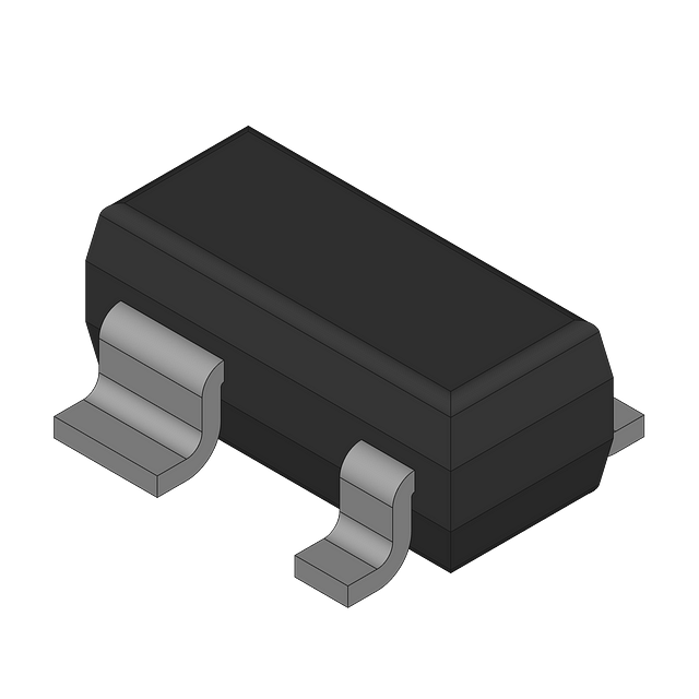
| 供应商器件封装 | SOT-143B |
| 其它名称 | 568-6938-1 |
| 包装 | 剪切带 (CT) |
| 安装类型 | 表面贴装 |
| 封装/外壳 | TO-253-4,TO-253AA |
| 应用 | 电流镜像 |
| 晶体管类型 | 2 PNP(双)电流反射镜 |
| 标准包装 | 1 |
| 电压-额定 | 30V |
| 额定电流 | 100mA |


PDF Datasheet 数据手册内容提取
BCV62 PNP general-purpose double transistors Rev. 4 — 26 July 2010 Product data sheet 1. Product profile 1.1 General description PNP general-purpose double transistors in a small SOT143B Surface-Mounted Device(SMD) plastic package. Table 1. Product overview Type number Package NPN complement Nexperia JEITA BCV62 SOT143B - BCV61 BCV62A BCV61A BCV62B BCV61B BCV62C BCV61C 1.2 Features and benefits (cid:132) Low current(max.100mA) (cid:132) Low voltage (max.30V) (cid:132) Matched pairs (cid:132) AEC-Q101 qualified (cid:132) Small SMD plastic package 1.3 Applications (cid:132) Applications with working point independent of temperature (cid:132) Current mirrors 1.4 Quick reference data Table 2. Quick reference data Symbol Parameter Conditions Min Typ Max Unit Per transistor V collector-emitter voltage open base - - −30 V CEO I collector current - - −100 mA C Transistor TR1 h DCcurrent gain V =−5V; I =−100μA 100 - - FE CE C V =−5V; I =−2mA 100 - 800 CE C
BCV62 Nexperia PNP general-purpose double transistors Table 2. Quick reference data …continued Symbol Parameter Conditions Min Typ Max Unit Transistor TR2 h DCcurrent gain V =−5V; I =−2mA FE CE C BCV62 100 - 800 BCV62A 100 - 250 BCV62B 220 - 475 BCV62C 420 - 800 2. Pinning information Table 3. Pinning Pin Description Simplified outline Graphic symbol 1 collectorTR2; baseTR1andTR2 4 3 4 3 2 collectorTR1 3 emitterTR1 TR2 TR1 4 emitterTR2 1 2 1 2 006aaa843 3. Ordering information Table 4. Ordering information Type number Package Name Description Version BCV62 - plastic surface-mounted package; 4leads SOT143B BCV62A BCV62B BCV62C 4. Marking Table 5. Marking codes Type number Marking code[1] BCV62 3M* BCV62A 3J* BCV62B 3K* BCV62C 3L* [1] * = -: made in Hong Kong * = p: made in Hong Kong * = t: made in Malaysia * = W: made in China BCV62 All information provided in this document is subject to legal disclaimers. © Nexperia B.V. 2017. All rights reserved Product data sheet Rev. 4 — 26 July 2010 2 of 14
BCV62 Nexperia PNP general-purpose double transistors 5. Limiting values Table 6. Limiting values In accordance with the Absolute Maximum Rating System (IEC 60134). Symbol Parameter Conditions Min Max Unit Per transistor V collector-base voltage open emitter - −30 V CBO V collector-emitter voltage open base - −30 V CEO V emitter-base voltage V =0V - −6 V EBS CE I collector current - −100 mA C I peak collector current - −200 mA CM I peak base current - −200 mA BM Per device P total power dissipation T ≤25°C [1] - 250 mW tot amb T junction temperature - 150 °C j T ambient temperature −65 +150 °C amb T storage temperature −65 +150 °C stg [1] Device mounted on an FR4Printed-Circuit Board(PCB). 6. Thermal characteristics Table 7. Thermal characteristics Symbol Parameter Conditions Min Typ Max Unit R thermal resistance from junction in free air [1] - - 500 K/W th(j-a) to ambient [1] Device mounted on an FR4PCB. 7. Characteristics Table 8. Characteristics T =25°C unless otherwise specified. j Symbol Parameter Conditions Min Typ Max Unit Transistor TR1 I collector-base V =−30V; I =0A - - −15 nA CBO CB E cut-offcurrent V =−30V; I =0A; - -− 5 μA CB E T =150°C j I emitter-base V =−5V; I =0A - - −100 nA EBO EB C cut-offcurrent h DCcurrent gain V =−5V; 100 - - FE CE I =−100μA C V =−5V; I =−2mA 100 - 800 CE C V collector-emitter I =−10mA; - −75 −300 mV CEsat C saturationvoltage I =−0.5mA B I =−100mA; - −250 −650 mV C I =−5mA B BCV62 All information provided in this document is subject to legal disclaimers. © Nexperia B.V. 2017. All rights reserved Product data sheet Rev. 4 — 26 July 2010 3 of 14
BCV62 Nexperia PNP general-purpose double transistors Table 8. Characteristics …continued T =25°C unless otherwise specified. j Symbol Parameter Conditions Min Typ Max Unit V base-emitter I =−10mA; [1] - −700 - mV BEsat C saturationvoltage I =−0.5mA B I =−100mA; [1] - −850 - mV C I =−5mA B V base-emitter voltage I =−2mA; V =−5V [2] −600 −650 −750 mV BE C CE I =−10mA; V =−5V [2] - -− 820 mV C CE f transition frequency V =−5V; 100 - - MHz T CE I =−10mA; C f=100MHz C collector capacitance V =−10V; - 4.5 - pF c CB I =i =0A E e NF noise figure V =−5V; - - 10 dB CE I =−200μA; R =2kΩ; C S f=1kHz; B=200Hz Transistor TR2 V emitter-base voltage V =0V; I =−250mA - - −1.5 V EBS CB E V =0V; I =−10μA −400 - - mV CB E h DCcurrent gain V =−5V; I =−2mA FE CE C BCV62 100 - 800 BCV62A 100 - 250 BCV62B 220 - 475 BCV62C 420 - 800 Transistors TR1 and TR2 I /I current matching I =−0.5mA; C1 E2 E2 V =−5V; CE1 T ≤25°C 0.7 - 1.3 amb T ≤150°C 0.7 - 1.3 amb I emitter current2 V =−5V [3] - -− 5 mA E2 CE1 [1] V decreases by about 1.7mV/K with increasing temperature. BEsat [2] V decreases by about 2mV/K with increasing temperature. BE [3] Device, without emitter resistors, mounted on an FR4PCB. BCV62 All information provided in this document is subject to legal disclaimers. © Nexperia B.V. 2017. All rights reserved Product data sheet Rev. 4 — 26 July 2010 4 of 14
BCV62 Nexperia PNP general-purpose double transistors 500 mgt711 −1200 mgt712 VBE hFE (mV) −1000 400 (1) (1) −800 300 (2) −600 200 (2) (3) −400 (3) 100 −200 0 0 −10−2 −10−1 −1 −10 −102 −103 −10−2 −10−1 −1 −10 −102 −103 IC (mA) IC (mA) VCE=−5V VCE=−5V (1) Tamb=150°C (1) Tamb=−55°C (2) Tamb=25°C (2) Tamb=25°C (3) Tamb=−55°C (3) Tamb=150°C Fig 1. BCV62A: DCcurrent gain as a function of Fig 2. BCV62A: Base-emitter voltage as a function of collector current; typical values collector current; typical values −104 mgt713 −1200 mgt714 VBEsat (mV) VCEsat (mV) −1000 (1) −103 −800 (2) (3) −600 −102 −400 (1) (3) (2) −200 −10 0 −10−1 −1 −10 −102 −103 −10−1 −1 −10 −102 −103 IC (mA) IC (mA) I /I =20 I /I =20 C B C B (1) Tamb=150°C (1) Tamb=−55°C (2) Tamb=25°C (2) Tamb=25°C (3) Tamb=−55°C (3) Tamb=150°C Fig 3. BCV62A: Collector-emitter saturation voltage Fig 4. BCV62A: Base-emitter saturation voltage as a as a function of collector current; typical function of collector current; typical values values BCV62 All information provided in this document is subject to legal disclaimers. © Nexperia B.V. 2017. All rights reserved Product data sheet Rev. 4 — 26 July 2010 5 of 14
BCV62 Nexperia PNP general-purpose double transistors 1000 mgt715 −1200 mgt716 VBE hFE (mV) −1000 800 (1) −800 600 (2) (1) −600 400 (2) −400 (3) 200 (3) −200 0 0 −10−2 −10−1 −1 −10 −102 −103 −10−2 −10−1 −1 −10 −102 −103 IC (mA) IC (mA) VCE=−5V VCE=−5V (1) Tamb=150°C (1) Tamb=−55°C (2) Tamb=25°C (2) Tamb=25°C (3) Tamb=−55°C (3) Tamb=150°C Fig 5. BCV62B: DCcurrent gain as a function of Fig 6. BCV62B: Base-emitter voltage as a function of collector current; typical values collector current; typical values −104 mgt717 −1200 mgt718 VBEsat (mV) VCEsat (mV) −1000 (1) −103 −800 (2) −600 (3) −102 −400 (1) −200 (3) (2) −10 0 −10−1 −1 −10 −102 −103 −10−1 −1 −10 −102 −103 IC (mA) IC (mA) I /I =20 I /I =20 C B C B (1) Tamb=150°C (1) Tamb=−55°C (2) Tamb=25°C (2) Tamb=25°C (3) Tamb=−55°C (3) Tamb=150°C Fig 7. BCV62B: Collector-emitter saturation voltage Fig 8. BCV62B: Base-emitter saturation voltage as a as a function of collector current; typical function of collector current; typical values values BCV62 All information provided in this document is subject to legal disclaimers. © Nexperia B.V. 2017. All rights reserved Product data sheet Rev. 4 — 26 July 2010 6 of 14
BCV62 Nexperia PNP general-purpose double transistors 1000 mgt719 −1200 mgt720 VBE hFE (mV) (1) −1000 800 (1) −800 600 (2) (2) −600 400 −400 (3) (3) 200 −200 0 0 −10−2 −10−1 −1 −10 −102 −103 −10−1 −1 −10 −102 −103 IC (mA) IC (mA) VCE=−5V VCE=−5V (1) Tamb=150°C (1) Tamb=−55°C (2) Tamb=25°C (2) Tamb=25°C (3) Tamb=−55°C (3) Tamb=150°C Fig 9. BCV62C: DCcurrent gain as a function of Fig 10. BCV62C: Base-emitter voltage as a function of collector current; typical values collector current; typical values −104 mgt721 −1200 mgt722 VBEsat (mV) VCEsat (mV) −1000 (1) −103 −800 (2) −600 (3) −102 −400 (1) −200 (3) (2) −10 0 −10−1 −1 −10 −102 −103 −10−1 −1 −10 −102 −103 IC (mA) IC (mA) I /I =20 I /I =20 C B C B (1) Tamb=150°C (1) Tamb=−55°C (2) Tamb=25°C (2) Tamb=25°C (3) Tamb=−55°C (3) Tamb=150°C Fig 11. BCV62C: Collector-emitter saturation voltage Fig 12. BCV62C: Base-emitter saturation voltage as a as a function of collector current; typical function of collector current; typical values values BCV62 All information provided in this document is subject to legal disclaimers. © Nexperia B.V. 2017. All rights reserved Product data sheet Rev. 4 — 26 July 2010 7 of 14
BCV62 Nexperia PNP general-purpose double transistors −30 mbk083 −VCE1max IE2 = (V) 1 mA −20 5 mA 10 mA −10 50 mA 0 10−1 1 10 RE (Ω) 102 I /I =1.3 C1 E2 Fig 13. Maximum collector-emitter voltage as a function of emitter resistor (seeFigure15) 8. Test information A IC1 2 1 −VCE1 TR1 TR2 IE2 = constant 3 4 006aaa841 Fig 14. Test circuit current matching A IC1 2 1 −VCE1 TR1 TR2 IE2 = constant 3 4 RE RE 006aac001 Fig 15. Current mirror with emitter resistors BCV62 All information provided in this document is subject to legal disclaimers. © Nexperia B.V. 2017. All rights reserved Product data sheet Rev. 4 — 26 July 2010 8 of 14
BCV62 Nexperia PNP general-purpose double transistors 8.1 Quality information This product has been qualified in accordance with the Automotive Electronics Council (AEC) standard Q101 - Stress test qualification for discrete semiconductors, and is suitable for use in automotive applications. 9. Package outline 3.0 2.8 1.1 1.9 0.9 4 3 0.45 0.15 2.5 1.4 2.1 1.2 1 2 0.88 0.48 0.15 0.78 0.38 0.09 1.7 Dimensions in mm 04-11-16 Fig 16. Package outline SOT143B 10. Packing information Table 9. Packing methods The indicated -xxx are the last three digits of the 12NC ordering code.[1] Type number Package Description Packing quantity 3000 10000 BCV62 SOT143B 4mm pitch, 8mm tape and reel -215 -235 BCV62A BCV62B BCV62C [1] For further information and the availability of packing methods, see Section14. BCV62 All information provided in this document is subject to legal disclaimers. © Nexperia B.V. 2017. All rights reserved Product data sheet Rev. 4 — 26 July 2010 9 of 14
BCV62 Nexperia PNP general-purpose double transistors 11. Soldering 3.25 0.6 (3×) 0.5 (3×) 1.9 solder lands 0.7 0.6 (3×) (3×) solder resist 2 3 solder paste occupied area 0.7 0.6 Dimensions in mm 0.75 0.95 0.9 1 sot143b_fr Fig 17. Reflow soldering footprint SOT143B 4.45 2.2 1.2 (3×) 1.425 (3×) solder lands solder resist 4.6 2.575 occupied area Dimensions in mm 1.425 preferred transport direction during soldering 1 1.2 sot143b_fw Fig 18. Wave soldering footprint SOT143B BCV62 All information provided in this document is subject to legal disclaimers. © Nexperia B.V. 2017. All rights reserved Product data sheet Rev. 4 — 26 July 2010 10 of 14
BCV62 Nexperia PNP general-purpose double transistors 12. Revision history Table 10. Revision history Document ID Release date Data sheet status Change notice Supersedes BCV62 v.4 20100726 Product data sheet - BCV62_3 Modifications: • The format of this data sheet has been redesigned to comply with the new identity guidelines of NXP Semiconductors. • Legal texts have been adapted to the new company name where appropriate. • Section 1 “Product profile”: amended • Section 3 “Ordering information”: added • Section 4 “Marking”: updated • Figure1, 2, 3, 4, 5, 6, 7, 8, 9, 10, 11 and 12: added • Section 8 “Test information”: added • Figure16: superseded by minimized package outline drawing • Section 10 “Packing information”: added • Section 11 “Soldering”: added • Section 13 “Legal information”: updated BCV62_3 19990408 Product specification - BCV62_CNV_2 BCV62_CNV_2 19970618 Product specification - - BCV62 All information provided in this document is subject to legal disclaimers. © Nexperia B.V. 2017. All rights reserved Product data sheet Rev. 4 — 26 July 2010 11 of 14
BCV62 Nexperia PNP general-purpose double transistors 13. Legal information 13.1 Data sheet status Document status[1][2] Product status[3] Definition Objective [short] data sheet Development This document contains data from the objective specification for product development. Preliminary [short] data sheet Qualification This document contains data from the preliminary specification. Product [short] data sheet Production This document contains the product specification. [1] Please consult the most recently issued document before initiating or completing a design. [2] The term ‘short data sheet’ is explained in section “Definitions”. [3] The product status of device(s) described in this document may have changed since this document was published and may differ in case of multiple devices. The latest product status information is available on the Internet at URL http://www.nexperia.com. 13.2 Definitions malfunction of a Nexperia product can reasonably be expected to result in personal injury, death or severe property or environmental damage. Nexperia accepts no liability for inclusion and/or use of Draft — The document is a draft version only. The content is still under Nexperia products in such equipment or applications and internal review and subject to formal approval, which may result in therefore such inclusion and/or use is at the customer’s own risk. modifications or additions. Nexperia does not give any representations or warranties as to the accuracy or completeness of Applications — Applications that are described herein for any of these information included herein and shall have no liability for the consequences of products are for illustrative purposes only. Nexperia makes no use of such information. representation or warranty that such applications will be suitable for the specified use without further testing or modification. Short data sheet — A short data sheet is an extract from a full data sheet with the same product type number(s) and title. A short data sheet is intended Customers are responsible for the design and operation of their applications for quick reference only and should not be relied upon to contain detailed and and products using Nexperia products, and Nexperia full information. For detailed and full information see the relevant full data accepts no liability for any assistance with applications or customer product sheet, which is available on request via the local Nexperia sales design. It is customer’s sole responsibility to determine whether the Nexperia office. In case of any inconsistency or conflict with the short data sheet, the product is suitable and fit for the customer’s applications and full data sheet shall prevail. products planned, as well as for the planned application and use of customer’s third party customer(s). Customers should provide appropriate Product specification — The information and data provided in a Product design and operating safeguards to minimize the risks associated with their data sheet shall define the specification of the product as agreed between applications and products. Nexperia and its customer, unless Nexperia and Nexperia does not accept any liability related to any default, customer have explicitly agreed otherwise in writing. In no event however, damage, costs or problem which is based on any weakness or default in the shall an agreement be valid in which the Nexperia product is customer’s applications or products, or the application or use by customer’s deemed to offer functions and qualities beyond those described in the third party customer(s). Customer is responsible for doing all necessary Product data sheet. testing for the customer’s applications and products using Nexperia products in order to avoid a default of the applications and 13.3 Disclaimers the products or of the application or use by customer’s third party customer(s). Nexperia does not accept any liability in this respect. Limited warranty and liability — Information in this document is believed to Limiting values — Stress above one or more limiting values (as defined in be accurate and reliable. However, Nexperia does not give any the Absolute Maximum Ratings System of IEC60134) will cause permanent representations or warranties, expressed or implied, as to the accuracy or damage to the device. Limiting values are stress ratings only and (proper) completeness of such information and shall have no liability for the operation of the device at these or any other conditions above those given in consequences of use of such information. the Recommended operating conditions section (if present) or the Characteristics sections of this document is not warranted. Constant or In no event shall Nexperia be liable for any indirect, incidental, repeated exposure to limiting values will permanently and irreversibly affect punitive, special or consequential damages (including - without limitation - lost the quality and reliability of the device. profits, lost savings, business interruption, costs related to the removal or replacement of any products or rework charges) whether or not such Terms and conditions of commercial sale — Nexperia damages are based on tort (including negligence), warranty, breach of products are sold subject to the general terms and conditions of commercial contract or any other legal theory. sale, as published at http://www.nexperia.com/profile/terms, unless otherwise agreed in a valid written individual agreement. In case an individual Notwithstanding any damages that customer might incur for any reason agreement is concluded only the terms and conditions of the respective whatsoever, Nexperia’s aggregate and cumulative liability towards agreement shall apply. Nexperia hereby expressly objects to customer for the products described herein shall be limited in accordance with the Terms and conditions of commercial sale of Nexperia. applying the customer’s general terms and conditions with regard to the purchase of Nexperia products by customer. Right to make changes — Nexperia reserves the right to make changes to information published in this document, including without No offer to sell or license — Nothing in this document may be interpreted or limitation specifications and product descriptions, at any time and without construed as an offer to sell products that is open for acceptance or the grant, notice. This document supersedes and replaces all information supplied prior conveyance or implication of any license under any copyrights, patents or to the publication hereof. other industrial or intellectual property rights. Suitability for use — Nexperia products are not designed, Export control — This document as well as the item(s) described herein authorized or warranted to be suitable for use in life support, life-critical or may be subject to export control regulations. Export might require a prior safety-critical systems or equipment, nor in applications where failure or authorization from national authorities. BCV62 All information provided in this document is subject to legal disclaimers. © Nexperia B.V. 2017. All rights reserved Product data sheet Rev. 4 — 26 July 2010 12 of 14
BCV62 Nexperia PNP general-purpose double transistors Quick reference data — The Quick reference data is an extract of the 13.4 Trademarks product data given in the Limiting values and Characteristics sections of this document, and as such is not complete, exhaustive or legally binding. Notice: All referenced brands, product names, service names and trademarks are the property of their respective owners. 14. Contact information For more information, please visit: http://www.nexperia.com For sales office addresses, please send an email to: salesaddresses@nexperia.com BCV62 All information provided in this document is subject to legal disclaimers. © Nexperia B.V. 2017. All rights reserved Product data sheet Rev. 4 — 26 July 2010 13 of 14
BCV62 Nexperia PNP general-purpose double transistors 15. Contents 1 Product profile. . . . . . . . . . . . . . . . . . . . . . . . . . 1 1.1 General description . . . . . . . . . . . . . . . . . . . . . 1 1.2 Features and benefits. . . . . . . . . . . . . . . . . . . . 1 1.3 Applications . . . . . . . . . . . . . . . . . . . . . . . . . . . 1 1.4 Quick reference data . . . . . . . . . . . . . . . . . . . . 1 2 Pinning information. . . . . . . . . . . . . . . . . . . . . . 2 3 Ordering information. . . . . . . . . . . . . . . . . . . . . 2 4 Marking. . . . . . . . . . . . . . . . . . . . . . . . . . . . . . . . 2 5 Limiting values. . . . . . . . . . . . . . . . . . . . . . . . . . 3 6 Thermal characteristics . . . . . . . . . . . . . . . . . . 3 7 Characteristics. . . . . . . . . . . . . . . . . . . . . . . . . . 3 8 Test information. . . . . . . . . . . . . . . . . . . . . . . . . 8 8.1 Quality information . . . . . . . . . . . . . . . . . . . . . . 9 9 Package outline. . . . . . . . . . . . . . . . . . . . . . . . . 9 10 Packing information . . . . . . . . . . . . . . . . . . . . . 9 11 Soldering . . . . . . . . . . . . . . . . . . . . . . . . . . . . . 10 12 Revision history. . . . . . . . . . . . . . . . . . . . . . . . 11 13 Legal information. . . . . . . . . . . . . . . . . . . . . . . 12 13.1 Data sheet status . . . . . . . . . . . . . . . . . . . . . . 12 13.2 Definitions. . . . . . . . . . . . . . . . . . . . . . . . . . . . 12 13.3 Disclaimers. . . . . . . . . . . . . . . . . . . . . . . . . . . 12 13.4 Trademarks. . . . . . . . . . . . . . . . . . . . . . . . . . . 13 14 Contact information. . . . . . . . . . . . . . . . . . . . . 13 15 Contents. . . . . . . . . . . . . . . . . . . . . . . . . . . . . . 14 © Nexperia B.V. 2017. All rights reserved For more information, please visit: http://www.nexperia.com For sales office addresses, please send an email to: salesaddresses@nexperia.com Date of release: 26 July 2010