 Datasheet下载
- 型号: BAP55LX,315
- 制造商: NXP Semiconductors
- 库位|库存: xxxx|xxxx
- 要求:
| 数量阶梯 | 香港交货 | 国内含税 |
| +xxxx | $xxxx | ¥xxxx |
查看当月历史价格
查看今年历史价格
BAP55LX,315产品简介:
ICGOO电子元器件商城为您提供BAP55LX,315由NXP Semiconductors设计生产,在icgoo商城现货销售,并且可以通过原厂、代理商等渠道进行代购。 BAP55LX,315价格参考。NXP SemiconductorsBAP55LX,315封装/规格:二极管 - 射频, RF Diode PIN - Single 50V 100mA 135mW 2-DFN1006D (0.6x1.0)。您可以下载BAP55LX,315参考资料、Datasheet数据手册功能说明书,资料中有BAP55LX,315 详细功能的应用电路图电压和使用方法及教程。
BAP55LX,315 是由 NXP USA Inc. 生产的一款射频二极管,主要应用于高频和射频电路中。该型号的二极管具有低电容、高开关速度和低反向恢复时间的特点,使其在多种射频应用中表现出色。

 应用场景:

1. 射频开关:
   BAP55LX,315 适用于各种射频开关电路,特别是在无线通信设备中,如手机、基站、Wi-Fi 路由器等。它能够快速切换信号路径,确保信号传输的高效性和稳定性。

2. 功率放大器保护:
   在射频功率放大器中,BAP55LX,315 可以用于保护电路,防止因过载或异常情况导致的损坏。它能够在短时间内快速响应,切断异常电流,从而保护放大器和其他敏感元件。

3. 天线调谐:
   在射频前端模块中,BAP55LX,315 可以用于天线调谐电路,帮助优化天线的匹配性能。通过动态调整天线的阻抗,它可以提高信号的传输效率,减少能量损失。

4. 频率合成器:
   在频率合成器中,BAP55LX,315 可以用于实现快速的频率切换和调谐功能。它能够提供稳定的开关特性,确保频率合成器在不同工作频率下的稳定性和准确性。

5. 雷达系统:
   在雷达系统中,BAP55LX,315 可以用于发射和接收电路中的开关控制。它能够在高速下可靠地切换信号路径,确保雷达系统的正常运行,并提高探测精度。

6. 卫星通信:
   在卫星通信系统中,BAP55LX,315 可以用于地面站和卫星之间的信号传输路径控制。它能够承受极端的工作环境,并提供稳定的性能,确保通信链路的可靠性。

7. 物联网(IoT)设备:
   在物联网设备中,BAP55LX,315 可以用于低功耗射频模块的设计。它能够有效降低功耗,延长电池寿命,同时保持高效的信号传输能力。

8. 汽车电子:
   在汽车电子领域,BAP55LX,315 可以用于车载通信系统、雷达传感器等设备中。它能够在复杂的电磁环境中保持稳定的性能,确保车辆的安全性和可靠性。

总之,BAP55LX,315 凭借其优异的射频性能和可靠性,广泛应用于各种高频和射频电路中,尤其适合对速度、效率和稳定性有较高要求的应用场景。
| 参数 | 数值 |
| 产品目录 | |
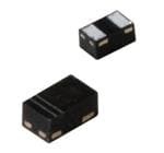
| 描述 | DIODE SILICON PIN SOD-882DPIN 二极管 RF Pin Diode |
| 产品分类 | RF 二极管分离式半导体 |
| 品牌 | NXP Semiconductors |
| 产品手册 | |
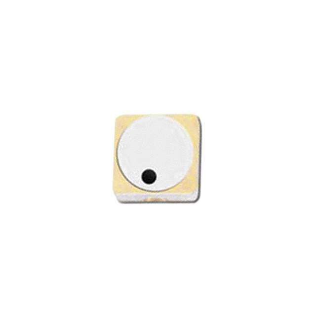
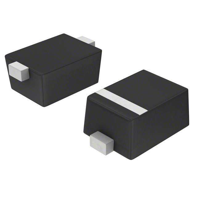
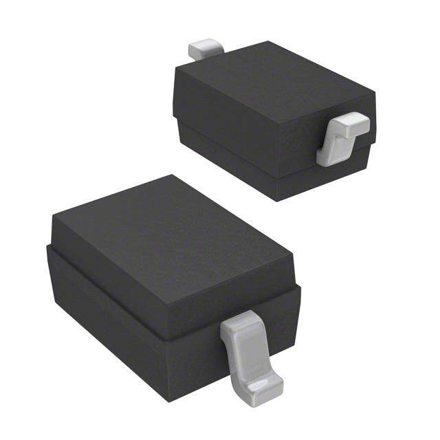
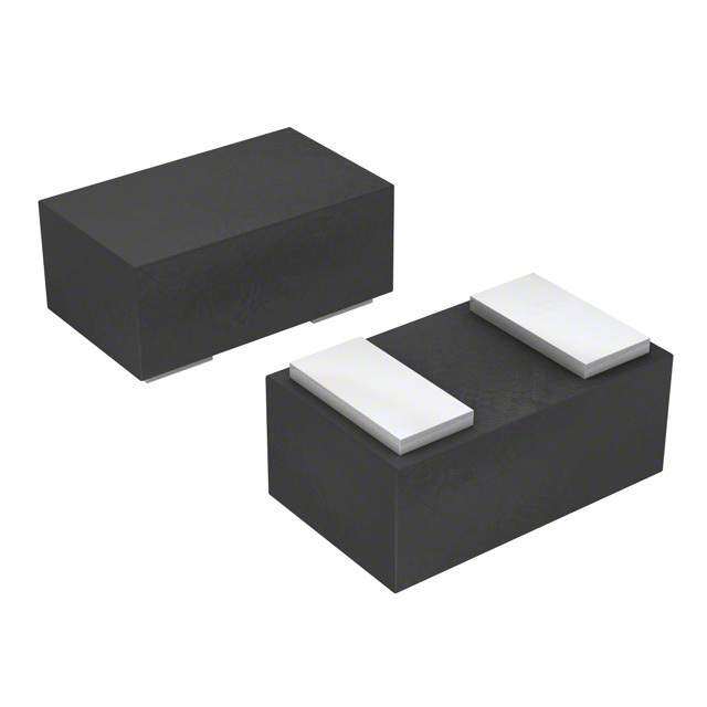
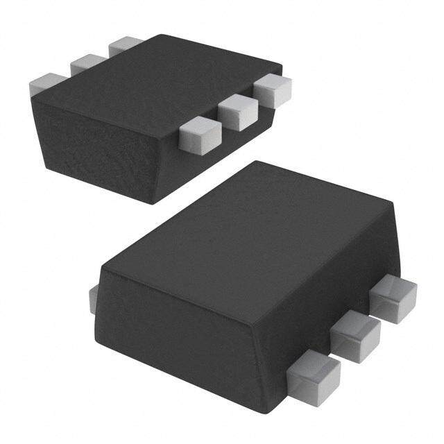
| 产品图片 |
|
| rohs | 符合RoHS无铅 / 符合限制有害物质指令(RoHS)规范要求 |
| 产品系列 | 二极管与整流器,PIN 二极管,NXP Semiconductors BAP55LX,315- |
| 数据手册 | |
| 产品型号 | BAP55LX,315 |
| PCN封装 | |
| PCN组件/产地 | |
| 不同 If、F时的电阻 | 800 毫欧 @ 100mA,100MHz |
| 不同 Vr、F时的电容 | 0.28pF @ 20V,1MHz |
| 二极管类型 | PIN - 单 |
| 产品种类 | PIN 二极管 |
| 供应商器件封装 | SOD882D |
| 其它名称 | 568-8536-1 |
| 功率耗散 | 135 mW |
| 功率耗散(最大值) | 135mW |
| 包装 | 剪切带 (CT) |
| 反向电压 | 50 V |
| 商标 | NXP Semiconductors |
| 安装风格 | SMD/SMT |
| 封装 | Reel |
| 封装/外壳 | SOD-882D |
| 封装/箱体 | SOD-882T |
| 工厂包装数量 | 15000 |
| 最大串联电阻(中频最大时) | 0.8 Ohms at 100 mA |
| 最大串联电阻(中频最小时) | 4.5 Ohms at 0.5 mA |
| 最大二极管电容 | 0.28 pF at 20 V |
| 最大工作温度 | + 150 C |
| 最小工作温度 | - 65 C |
| 标准包装 | 1 |
| 正向电压 | 1.1 V at 50 mA |
| 正向电流 | 100 mA |
| 电压-峰值反向(最大值) | 50V |
| 电流-最大值 | 100mA |
| 类型 | Planar |
| 配置 | Single |
| 零件号别名 | BAP55LX T/R |
| 频率范围 | UHF, SHF |


PDF Datasheet 数据手册内容提取
BAP55LX DFN1006D-2 Silicon PIN diode Rev. 4 — 6 August 2013 Product data sheet 1. Product profile 1.1 General description Planar PIN diode in a SOD882D leadless ultra small plastic SMD package. 1.2 Features and benefits High speed switching for RF signals Low diode capacitance Low forward resistance Very low series inductance For applications up to 3GHz 1.3 Applications RF attenuators and switches 2. Pinning information Table 1. Discrete pinning Pin Description Simplified outline Symbol 1 cathode [1] 2 anode 1 2 Transparent sym006 top view [1] The marking bar indicates the cathode. 3. Ordering information Table 2. Ordering information Type number Package Name Description Version BAP55LX DFN1006D-2 leadless ultra small plastic package; 2 terminals; SOD882D body10.60.4mm
BAP55LX NXP Semiconductors Silicon PIN diode 4. Marking Table 3. Marking codes Type number Marking code[1] BAP55LX 1111 1101 [1] For SOD882D binary marking code description, see Figure1. 4.1 Binary marking code description CATHODE BAR READING DIRECTION VENDOR CODE READING EXAMPLE: 0111 1011 MARKING CODE (EXAMPLE) READING DIRECTION 006aac477 Fig 1. SOD882D binary marking code description example 5. Limiting values Table 4. Limiting values In accordance with the Absolute Maximum Rating System (IEC 60134). Symbol Parameter Conditions Min Max Unit V reverse voltage - 50 V R I forward current - 100 mA F P total power dissipation T = 90 C - 135 mW tot sp T storage temperature 65 +150 C stg T junction temperature 65 +150 C j 6. Thermal characteristics Table 5. Thermal characteristics Symbol Parameter Conditions Typ Unit R thermal resistance from junction 78 K/W th(j-sp) to solder point BAP55LX All information provided in this document is subject to legal disclaimers. © NXP B.V. 2013. All rights reserved. Product data sheet Rev. 4 — 6 August 2013 2 of 16
BAP55LX NXP Semiconductors Silicon PIN diode 7. Characteristics Table 6. Characterist ics T = 25 C unless otherwise specified. amb Symbol Parameter Conditions Min Typ Max Unit V forward voltage I =50mA - 0.95 1.1 V F F I reverse current V =20V - - 10 nA R R V =50V - - 100 nA R C diode capacitance seeFigure3; f=1MHz; d V =0V - 0.28 - pF R V =1V - 0.23 - pF R V =20V - 0.18 0.28 pF R r diode forward resistance seeFigure4; f=100MHz; D I =0.5mA - 3.3 4.5 F I =1mA - 2.2 3.3 F I =10mA - 0.8 1.2 F I =100mA - 0.5 0.8 F ISL isolation seeFigure5;V =0V; R f=900MHz - 19 - dB f=1800MHz - 14 - dB f=2450MHz - 12 - dB L insertion loss seeFigure6;I =0.5mA; ins F f=900MHz - 0.24 - dB f=1800MHz - 0.25 - dB f=2450MHz - 0.26 - dB L insertion loss seeFigure6;I =1mA; ins F f=900MHz - 0.17 - dB f=1800MHz - 0.18 - dB f=2450MHz - 0.19 - dB L insertion loss seeFigure6;I =10mA; ins F f=900MHz - 0.08 - dB f=1800MHz - 0.09 - dB f=2450MHz - 0.10 - dB L insertion loss seeFigure6;I =100mA; ins F f=900MHz - 0.05 - dB f=1800MHz - 0.07 - dB f=2450MHz - 0.08 - dB charge carrier life time when switched from I =10mA to 0.225 0.27 - s L F I =6mA; R =100; measured at R L I =3mA R L series inductance I =100mA; f=100MHz - 0.4 - nH S F BAP55LX All information provided in this document is subject to legal disclaimers. © NXP B.V. 2013. All rights reserved. Product data sheet Rev. 4 — 6 August 2013 3 of 16
BAP55LX NXP Semiconductors Silicon PIN diode 001aan470 0.5 Cd (pF) 0.4 0.3 0.2 0.1 0 0 1000 2000 3000 4000 f (MHz) VR=0 V; Tj=25C. Fig 2. Diode capacitance as a function of frequency; typical values 400 001aag762 102 001aag763 Cd (fF) rD (Ω) 300 10 200 1 100 0 10−1 0 5 10 15 20 10−1 1 10 102 VR (V) If (mA) f=1MHz; Tj=25C. f=100MHz; Tj=25C. Fig 3. Diode capacitance as a function of reverse Fig 4. Forward resistance as a function of forward voltage; typical values current; typical values BAP55LX All information provided in this document is subject to legal disclaimers. © NXP B.V. 2013. All rights reserved. Product data sheet Rev. 4 — 6 August 2013 4 of 16
BAP55LX NXP Semiconductors Silicon PIN diode 001aag764 001aag765 0 0 (1) ISL Lins (dB) (dB) (3) (2) −0.2 −10 (4) −0.4 −20 −0.6 −30 −0.8 −40 −1.0 0 1000 2000 3000 0 1000 2000 3000 f (MHz) f (MHz) Tamb=25C Tamb=25C Diode zero biased and inserted in series with a 50 (1) IF=100mA stripline circuit (2) IF=10mA (3) I =1mA F (4) IF=0.5mA Diode inserted in series with a 50 stripline circuit and biased via the analyzer Tee network Fig 5. Isolation of the diode as a function of Fig 6. Insertion loss of the diode as a function of frequency; typical values frequency; typical values BAP55LX All information provided in this document is subject to legal disclaimers. © NXP B.V. 2013. All rights reserved. Product data sheet Rev. 4 — 6 August 2013 5 of 16
BAP55LX NXP Semiconductors Silicon PIN diode 7.1 S-parameters 7.1.1 Diode in series configuration 90° 1.0 +1 135° +0.5 +2 45° 0.8 0.6 0.4 +0.2 +5 (5) (6) 0.2 (7) 180° 0 0.2 0.5 ((23)) 2 5 10 0° 0 (4) −0.2 −5 (1) −0.5 −2 −135° −45° −1 1.0 −90° 001aan345 Z0 = 50 ; f = 100 MHz to 10 GHz. (1) IF = 0 mA (2) I = 0.1 mA F (3) IF = 0.5 mA (4) IF = 1 mA (5) I = 5mA F (6) IF = 10 mA (7) IF = 100 mA Fig 7. Input reflection coefficient (S ); typical values 11 BAP55LX All information provided in this document is subject to legal disclaimers. © NXP B.V. 2013. All rights reserved. Product data sheet Rev. 4 — 6 August 2013 6 of 16
BAP55LX NXP Semiconductors Silicon PIN diode 90° 1.0 +1 135° +0.5 +2 45° 0.8 0.6 0.4 +0.2 +5 (5) (6) 0.2 (7) 180° 0 0.2 0.5 ((23)) 2 5 10 0° 0 (4) −0.2 −5 (1) −0.5 −2 −135° −45° −1 1.0 −90° 001aan347 Z0 = 50 ; f = 100 MHz to 10 GHz. (1) IF = 0 mA (2) I = 0.1 mA F (3) IF = 0.5 mA (4) IF = 1 mA (5) I = 5mA F (6) IF = 10 mA (7) IF = 100 mA Fig 8. Output reflection coefficient (S ); typical values 22 BAP55LX All information provided in this document is subject to legal disclaimers. © NXP B.V. 2013. All rights reserved. Product data sheet Rev. 4 — 6 August 2013 7 of 16
BAP55LX NXP Semiconductors Silicon PIN diode 90° 135° 45° (1) (2) (3) 180°−1.0 −0.8 −0.6 −0.4 −0.2 0 (4) 0° (5) (6) (7) −135° −45° −90° 001aan346 Z0 = 50 ; f = 100 MHz to 10 GHz. (1) IF = 0 mA (2) I = 0.1 mA F (3) IF = 0.5 mA (4) IF = 1 mA (5) I = 5mA F (6) IF = 10 mA (7) IF = 100 mA Fig 9. Forward transmission coefficient (S ); typical values 21 BAP55LX All information provided in this document is subject to legal disclaimers. © NXP B.V. 2013. All rights reserved. Product data sheet Rev. 4 — 6 August 2013 8 of 16
BAP55LX NXP Semiconductors Silicon PIN diode 7.1.2 Diode in parallel configuration 90° 1.0 +1 135° +0.5 +2 45° 0.8 0.6 0.4 (1) +5 (2) (3) 0.2 (4) (5) 180° 0 0.2 (6)0.5 1 2 5 10 0° 0 −0.2 −5 −0.5 −2 −135° −45° −1 1.0 −90° 001aan342 Z0 = 50 ; f = 100 MHz to 10 GHz. (1) IF = 0.1 mA (2) IF = 0.5 mA (3) I = 1 mA F (4) IF = 5mA (5) IF = 10 mA (6) I = 100 mA F Fig 10. Input reflection coefficient (S ); typical values 11 BAP55LX All information provided in this document is subject to legal disclaimers. © NXP B.V. 2013. All rights reserved. Product data sheet Rev. 4 — 6 August 2013 9 of 16
BAP55LX NXP Semiconductors Silicon PIN diode 90° 1.0 +1 135° +0.5 +2 45° 0.8 0.6 0.4 (1) +5 (2) (3) 0.2 (4) 180° 0 0.2 ((56)) 0.5 1 2 5 10 0° 0 −0.2 −5 −0.5 −2 −135° −45° −1 1.0 −90° 001aan344 Z0 = 50 ; f = 100 MHz to 10 GHz. (1) IF = 0.1 mA (2) I = 0.5 mA F (3) IF = 1 mA (4) IF = 5mA (5) I = 10 mA F (6) IF = 100 mA Fig 11. Output reflection coefficient (S ); typical values 22 BAP55LX All information provided in this document is subject to legal disclaimers. © NXP B.V. 2013. All rights reserved. Product data sheet Rev. 4 — 6 August 2013 10 of 16
BAP55LX NXP Semiconductors Silicon PIN diode 90° 135° 45° (1) (2) −1.0 −0.8 −0.6 −0.4 −0.2 0 (3) 180° (4) 0° (5) (6) −135° −45° −90° 001aan343 Z0 = 50 ; f = 100 MHz to 10 GHz. (1) IF = 0.1 mA (2) I = 0.5 mA F (3) IF = 1 mA (4) IF = 5mA (5) I = 10 mA F (6) IF = 100 mA Fig 12. Forward transmission coefficient (S ); typical values 21 BAP55LX All information provided in this document is subject to legal disclaimers. © NXP B.V. 2013. All rights reserved. Product data sheet Rev. 4 — 6 August 2013 11 of 16
BAP55LX NXP Semiconductors Silicon PIN diode 8. Package outline DFN1006D-2: Leadless ultra small plastic package; 2 terminals; body 1 x 0.6 x 0.4 mm SOD882D (2x) L1 w A (2x) 1 2 b (2x) (2x) w B e A A1 y E A D (2) B Dimensions 0 0.5 1 mm scale Unit A(1) A1 b D E e L1 w y max 0.4 0.04 0.55 0.65 1.05 0.30 0.1 0.03 mm nom 0.50 0.60 1.00 0.65 0.25 min 0.45 0.55 0.95 0.22 Note 1. Dimension including plating thickness. 2. The marking bar indicates the cathode (if applicable). sod882d_po Outline References European Issue date version IEC JEDEC JEITA projection 10-09-27 SOD882D 12-05-01 Fig 13. Package outline SOD882D (DFN1006D-2) BAP55LX All information provided in this document is subject to legal disclaimers. © NXP B.V. 2013. All rights reserved. Product data sheet Rev. 4 — 6 August 2013 12 of 16
BAP55LX NXP Semiconductors Silicon PIN diode 9. Abbreviations Table 7. Abbreviations Acronym Description PIN P-type, Intrinsic, N-type SMD Surface Mounted Device RF Radio Frequency 10. Revision history Table 8. Revision history Document ID Release date Data sheet status Change notice Supersedes BAP55LX v.4 20130806 Product data sheet - BAP55LX v.3 Modifications: • Section1.1 on page1: Changed package to SOD882D • Table1 on page1: Changed simplified outline to SOD882D • Table2 on page1: Changed package to SOD882D • Section4 on page2: Update ‘Marking’ section • Section8 on page12: Changed package to SOD882D BAP55LX v.3 20110113 Product data sheet - BAP55LX v.2 BAP55LX v.2 20101216 Product data sheet - BAP55LX v.1 BAP55LX v.1 20070730 Product data sheet - - BAP55LX All information provided in this document is subject to legal disclaimers. © NXP B.V. 2013. All rights reserved. Product data sheet Rev. 4 — 6 August 2013 13 of 16
BAP55LX NXP Semiconductors Silicon PIN diode 11. Legal information 11.1 Data sheet status Document status[1][2] Product status[3] Definition Objective [short] data sheet Development This document contains data from the objective specification for product development. Preliminary [short] data sheet Qualification This document contains data from the preliminary specification. Product [short] data sheet Production This document contains the product specification. [1] Please consult the most recently issued document before initiating or completing a design. [2] The term ‘short data sheet’ is explained in section “Definitions”. [3] The product status of device(s) described in this document may have changed since this document was published and may differ in case of multiple devices. The latest product status information is available on the Internet at URLhttp://www.nxp.com. 11.2 Definitions Suitability for use — NXP Semiconductors products are not designed, authorized or warranted to be suitable for use in life support, life-critical or safety-critical systems or equipment, nor in applications where failure or Draft — The document is a draft version only. The content is still under malfunction of an NXP Semiconductors product can reasonably be expected internal review and subject to formal approval, which may result in to result in personal injury, death or severe property or environmental modifications or additions. NXP Semiconductors does not give any damage. NXP Semiconductors and its suppliers accept no liability for representations or warranties as to the accuracy or completeness of inclusion and/or use of NXP Semiconductors products in such equipment or information included herein and shall have no liability for the consequences of applications and therefore such inclusion and/or use is at the customer’s own use of such information. risk. Short data sheet — A short data sheet is an extract from a full data sheet Applications — Applications that are described herein for any of these with the same product type number(s) and title. A short data sheet is intended products are for illustrative purposes only. NXP Semiconductors makes no for quick reference only and should not be relied upon to contain detailed and representation or warranty that such applications will be suitable for the full information. For detailed and full information see the relevant full data specified use without further testing or modification. sheet, which is available on request via the local NXP Semiconductors sales office. In case of any inconsistency or conflict with the short data sheet, the Customers are responsible for the design and operation of their applications full data sheet shall prevail. and products using NXP Semiconductors products, and NXP Semiconductors accepts no liability for any assistance with applications or customer product Product specification — The information and data provided in a Product design. It is customer’s sole responsibility to determine whether the NXP data sheet shall define the specification of the product as agreed between Semiconductors product is suitable and fit for the customer’s applications and NXP Semiconductors and its customer, unless NXP Semiconductors and products planned, as well as for the planned application and use of customer have explicitly agreed otherwise in writing. In no event however, customer’s third party customer(s). Customers should provide appropriate shall an agreement be valid in which the NXP Semiconductors product is design and operating safeguards to minimize the risks associated with their deemed to offer functions and qualities beyond those described in the applications and products. Product data sheet. NXP Semiconductors does not accept any liability related to any default, damage, costs or problem which is based on any weakness or default in the 11.3 Disclaimers customer’s applications or products, or the application or use by customer’s third party customer(s). Customer is responsible for doing all necessary testing for the customer’s applications and products using NXP Limited warranty and liability — Information in this document is believed to Semiconductors products in order to avoid a default of the applications and be accurate and reliable. However, NXP Semiconductors does not give any the products or of the application or use by customer’s third party representations or warranties, expressed or implied, as to the accuracy or customer(s). NXP does not accept any liability in this respect. completeness of such information and shall have no liability for the consequences of use of such information. NXP Semiconductors takes no Limiting values — Stress above one or more limiting values (as defined in responsibility for the content in this document if provided by an information the Absolute Maximum Ratings System of IEC60134) will cause permanent source outside of NXP Semiconductors. damage to the device. Limiting values are stress ratings only and (proper) operation of the device at these or any other conditions above those given in In no event shall NXP Semiconductors be liable for any indirect, incidental, the Recommended operating conditions section (if present) or the punitive, special or consequential damages (including - without limitation - lost Characteristics sections of this document is not warranted. Constant or profits, lost savings, business interruption, costs related to the removal or repeated exposure to limiting values will permanently and irreversibly affect replacement of any products or rework charges) whether or not such the quality and reliability of the device. damages are based on tort (including negligence), warranty, breach of contract or any other legal theory. Terms and conditions of commercial sale — NXP Semiconductors products are sold subject to the general terms and conditions of commercial Notwithstanding any damages that customer might incur for any reason whatsoever, NXP Semiconductors’ aggregate and cumulative liability towards sale, as published at http://www.nxp.com/profile/terms, unless otherwise customer for the products described herein shall be limited in accordance agreed in a valid written individual agreement. In case an individual with the Terms and conditions of commercial sale of NXP Semiconductors. agreement is concluded only the terms and conditions of the respective agreement shall apply. NXP Semiconductors hereby expressly objects to Right to make changes — NXP Semiconductors reserves the right to make applying the customer’s general terms and conditions with regard to the changes to information published in this document, including without purchase of NXP Semiconductors products by customer. limitation specifications and product descriptions, at any time and without notice. This document supersedes and replaces all information supplied prior No offer to sell or license — Nothing in this document may be interpreted or to the publication hereof. construed as an offer to sell products that is open for acceptance or the grant, conveyance or implication of any license under any copyrights, patents or other industrial or intellectual property rights. BAP55LX All information provided in this document is subject to legal disclaimers. © NXP B.V. 2013. All rights reserved. Product data sheet Rev. 4 — 6 August 2013 14 of 16
BAP55LX NXP Semiconductors Silicon PIN diode Export control — This document as well as the item(s) described herein NXP Semiconductors’ specifications such use shall be solely at customer’s may be subject to export control regulations. Export might require a prior own risk, and (c) customer fully indemnifies NXP Semiconductors for any authorization from competent authorities. liability, damages or failed product claims resulting from customer design and use of the product for automotive applications beyond NXP Semiconductors’ Non-automotive qualified products — Unless this data sheet expressly standard warranty and NXP Semiconductors’ product specifications. states that this specific NXP Semiconductors product is automotive qualified, the product is not suitable for automotive use. It is neither qualified nor tested Translations — A non-English (translated) version of a document is for in accordance with automotive testing or application requirements. NXP reference only. The English version shall prevail in case of any discrepancy Semiconductors accepts no liability for inclusion and/or use of between the translated and English versions. non-automotive qualified products in automotive equipment or applications. In the event that customer uses the product for design-in and use in 11.4 Trademarks automotive applications to automotive specifications and standards, customer (a) shall use the product without NXP Semiconductors’ warranty of the Notice: All referenced brands, product names, service names and trademarks product for such automotive applications, use and specifications, and (b) are the property of their respective owners. whenever customer uses the product for automotive applications beyond 12. Contact information For more information, please visit: http://www.nxp.com For sales office addresses, please send an email to: salesaddresses@nxp.com BAP55LX All information provided in this document is subject to legal disclaimers. © NXP B.V. 2013. All rights reserved. Product data sheet Rev. 4 — 6 August 2013 15 of 16
BAP55LX NXP Semiconductors Silicon PIN diode 13. Contents 1 Product profile. . . . . . . . . . . . . . . . . . . . . . . . . . 1 1.1 General description . . . . . . . . . . . . . . . . . . . . . 1 1.2 Features and benefits. . . . . . . . . . . . . . . . . . . . 1 1.3 Applications . . . . . . . . . . . . . . . . . . . . . . . . . . . 1 2 Pinning information. . . . . . . . . . . . . . . . . . . . . . 1 3 Ordering information. . . . . . . . . . . . . . . . . . . . . 1 4 Marking. . . . . . . . . . . . . . . . . . . . . . . . . . . . . . . . 2 4.1 Binary marking code description. . . . . . . . . . . . 2 5 Limiting values. . . . . . . . . . . . . . . . . . . . . . . . . . 2 6 Thermal characteristics . . . . . . . . . . . . . . . . . . 2 7 Characteristics. . . . . . . . . . . . . . . . . . . . . . . . . . 3 7.1 S-parameters . . . . . . . . . . . . . . . . . . . . . . . . . . 6 7.1.1 Diode in series configuration . . . . . . . . . . . . . . 6 7.1.2 Diode in parallel configuration . . . . . . . . . . . . . 9 8 Package outline. . . . . . . . . . . . . . . . . . . . . . . . 12 9 Abbreviations. . . . . . . . . . . . . . . . . . . . . . . . . . 13 10 Revision history. . . . . . . . . . . . . . . . . . . . . . . . 13 11 Legal information. . . . . . . . . . . . . . . . . . . . . . . 14 11.1 Data sheet status . . . . . . . . . . . . . . . . . . . . . . 14 11.2 Definitions. . . . . . . . . . . . . . . . . . . . . . . . . . . . 14 11.3 Disclaimers. . . . . . . . . . . . . . . . . . . . . . . . . . . 14 11.4 Trademarks. . . . . . . . . . . . . . . . . . . . . . . . . . . 15 12 Contact information. . . . . . . . . . . . . . . . . . . . . 15 13 Contents. . . . . . . . . . . . . . . . . . . . . . . . . . . . . . 16 Please be aware that important notices concerning this document and the product(s) described herein, have been included in section ‘Legal information’. © NXP B.V. 2013. All rights reserved. For more information, please visit: http://www.nxp.com For sales office addresses, please send an email to: salesaddresses@nxp.com Date of release: 6 August 2013 Document identifier: BAP55LX
Mouser Electronics Authorized Distributor Click to View Pricing, Inventory, Delivery & Lifecycle Information: N XP: BAP55LX,315