ICGOO在线商城 > 集成电路(IC) > PMIC - 稳压器 - 线性 > BA33BC0FP-E2
 Datasheet下载
- 型号: BA33BC0FP-E2
- 制造商: ROHM Semiconductor
- 库位|库存: xxxx|xxxx
- 要求:
| 数量阶梯 | 香港交货 | 国内含税 |
| +xxxx | $xxxx | ¥xxxx |
查看当月历史价格
查看今年历史价格
BA33BC0FP-E2产品简介:
ICGOO电子元器件商城为您提供BA33BC0FP-E2由ROHM Semiconductor设计生产,在icgoo商城现货销售,并且可以通过原厂、代理商等渠道进行代购。 BA33BC0FP-E2价格参考¥3.33-¥7.37。ROHM SemiconductorBA33BC0FP-E2封装/规格:PMIC - 稳压器 - 线性, Linear Voltage Regulator IC Positive Fixed 1 Output 3.3V 1A TO-252-3。您可以下载BA33BC0FP-E2参考资料、Datasheet数据手册功能说明书,资料中有BA33BC0FP-E2 详细功能的应用电路图电压和使用方法及教程。
BA33BC0FP-E2 是由罗姆半导体(Rohm Semiconductor)生产的一款 PMIC(电源管理集成电路),属于线性稳压器类别。该型号主要应用于需要高效、稳定电压输出的电子设备中,以下是其典型的应用场景:

1. 消费类电子产品
   - 适用于便携式设备,如智能手机、平板电脑、可穿戴设备等。这些设备对低功耗和小型化设计有较高要求,而 BA33BC0FP-E2 的高集成度和低功耗特性能够满足需求。
   - 可用于音频设备(如耳机放大器、蓝牙音箱)中的电源管理,确保音频信号的稳定性和清晰度。

2. 通信设备
   - 在无线模块(如 Wi-Fi、蓝牙、Zigbee 等)中提供稳定的电源供应,保证通信质量。
   - 应用于物联网(IoT)设备,为传感器节点或数据采集单元供电,支持长时间运行。

3. 工业控制与自动化
   - 用于工业级微控制器(MCU)或数字信号处理器(DSP)的供电,确保系统在复杂环境下仍能保持高可靠性。
   - 适用于远程监控设备、数据记录仪等需要低噪声电源的应用。

4. 汽车电子
   - 可用于车载信息娱乐系统、导航设备以及仪表盘显示模块中,提供精确的电压调节。
   - 支持车内低功耗子系统的供电需求,例如环境光传感器、温度传感器等。

5. 医疗设备
   - 在便携式医疗设备(如血糖仪、脉搏血氧仪)中提供稳定的电源,确保测量结果的准确性。
   - 用于健康监测设备的电池管理,延长设备续航时间。

6. 嵌入式系统
   - 为各种嵌入式模块(如 RFID 阅读器、GPS 模块)提供高效的电源管理方案。
   - 支持多通道电压输出,简化复杂系统的电源设计。

BA33BC0FP-E2 的特点包括低 dropout(低压差)、高精度输出电压、内置保护功能(如过热保护、短路保护)等,使其能够在多种应用场景中表现出色,同时满足不同设备对电源性能的要求。
| 参数 | 数值 |
| 产品目录 | 集成电路 (IC)半导体 |
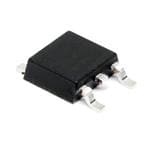
| 描述 | IC REG LDO 3.3V 1A TO252-3低压差稳压器 IC LDO 1A 3.3V |
| 产品分类 | |
| 品牌 | Rohm Semiconductor |
| 产品手册 | |
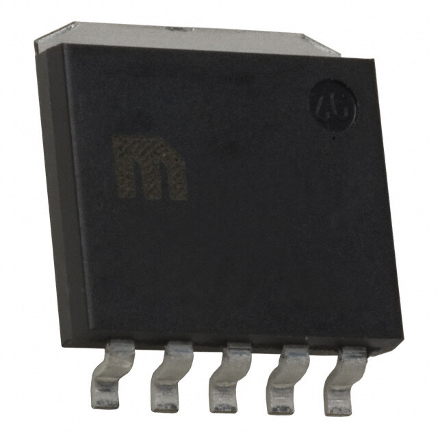
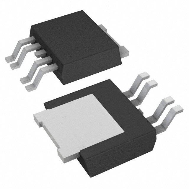
| 产品图片 |
|
| rohs | 符合RoHS无铅 / 符合限制有害物质指令(RoHS)规范要求 |
| 产品系列 | 电源管理 IC,低压差稳压器,ROHM Semiconductor BA33BC0FP-E2- |
| 数据手册 | |
| 产品型号 | BA33BC0FP-E2 |
| 产品培训模块 | http://www.digikey.cn/PTM/IndividualPTM.page?site=cn&lang=zhs&ptm=30333 |
| 产品种类 | 低压差稳压器 |
| 供应商器件封装 | TO-252-3 |
| 其它名称 | BA33BC0FP-E2CT |
| 包装 | 剪切带 (CT) |
| 参考电压 | 1.28 V |
| 商标 | ROHM Semiconductor |
| 回动电压—最大值 | 500 mV |
| 安装类型 | 表面贴装 |
| 安装风格 | SMD/SMT |
| 封装 | Reel |
| 封装/外壳 | TO-252-3,DPak(2 引线+接片),SC-63 |
| 封装/箱体 | TO-252-3 |
| 工作温度 | -40°C ~ 105°C |
| 工厂包装数量 | 2000 |
| 最大功率耗散 | 1.2 W |
| 最大工作温度 | + 105 C |
| 最大输入电压 | 16 V |
| 最小工作温度 | - 40 C |
| 最小输入电压 | + 4.3 V |
| 标准包装 | 1 |
| 特色产品 | http://www.digikey.cn/product-highlights/cn/zh/rohm-ba-bd-ldo-regulator-ics/3995 |
| 电压-跌落(典型值) | 0.3V @ 200mA |
| 电压-输入 | 最高 16V |
| 电压-输出 | 3.3V |
| 电压调节准确度 | 2 % |
| 电流-输出 | 1A |
| 电流-限制(最小值) | - |
| 稳压器拓扑 | 正,固定式 |
| 稳压器数 | 1 |
| 线路调整率 | 35 mV |
| 负载调节 | 75 mV |
| 输出电压 | 3.3 V |
| 输出电流 | 1 A |
| 输出端数量 | 1 Output |
| 输出类型 | Fixed |


- 商务部:美国ITC正式对集成电路等产品启动337调查
- 曝三星4nm工艺存在良率问题 高通将骁龙8 Gen1或转产台积电
- 太阳诱电将投资9.5亿元在常州建新厂生产MLCC 预计2023年完工
- 英特尔发布欧洲新工厂建设计划 深化IDM 2.0 战略
- 台积电先进制程称霸业界 有大客户加持明年业绩稳了
- 达到5530亿美元!SIA预计今年全球半导体销售额将创下新高
- 英特尔拟将自动驾驶子公司Mobileye上市 估值或超500亿美元
- 三星加码芯片和SET,合并消费电子和移动部门,撤换高东真等 CEO
- 三星电子宣布重大人事变动 还合并消费电子和移动部门
- 海关总署:前11个月进口集成电路产品价值2.52万亿元 增长14.8%


PDF Datasheet 数据手册内容提取
Datasheet 1A Variable/Fixed Output LDO Regulators BAxxBC0 Series(Fixed) BAxxBC0W Series(Fixed) BA00BC0WCP-V5(Varia ble) ●General Description The BAxxBC0 are low-saturation regulators with an output current of 1.0 A and an output voltage accuracy of ±2%. A broad output voltage range is offered, from 1.5V to 10V, and built-in overcurrent protection and thermal shutdown (TSD) circuits prevent damage due to short-circuiting and overloading, respectively. ●Features ●Packages W (Typ.) x D (Typ.) x H (Max.) (cid:132) Output voltage accuracy: ±2% TO252-3 6.50mm x 9.50mm x 2.50mm Broad output range available: 1.5 V -10 V TO252-5 6.50mm x 9.50mm x 2.50mm (BAxxBC0 series) TO220CP-V5 10.00mm x 20.12mm x 4.60mm (cid:132) Low saturation-voltage type with PNP output TO220FP-3 10.00mm x 30.50mm x 4.60mm (cid:132) Built-in overcurrent protection circuit TO220FP-5 10.00mm x 30.50mm x 4.60mm (cid:132) Built-in thermal shutdown circuit TO220FP-5(V5) 10.00mm x 31.50mm x 8.15mm (cid:132) Integrated shutdown switch (BAxxBC0WT, BAxxBC0WT-5, or BAxxBC0WFP Series, BA00BC0WCP-V5) ●Key Specifications (cid:132) Input Power Supply Voltage: 16.0V(Max.) (cid:132) Output voltage:(BA00BC0xx) Variable (BAxxBC0) Fixed (cid:132) Output current: 1A(Max.) TO252-3 TO252-5 (cid:132) Shutdown current: 0μA(Typ.) (cid:132) Operating temperature range: -40℃ to +105℃ TO220CP-V5 ●Applications All electronic devices that use microcontrollers and logic circuits TO220FP-3 TO220FP-5 TO220FP-5 (V5) ●Lineup Matrix Output Voltage (V) Part Number Package 1.5 1.8 2.5 3.0 3.3 5.0 6.0 7.0 8.0 9.0 10.0 Variable BAxxBC0WT (cid:123) (cid:123) (cid:123) (cid:123) (cid:123) (cid:123) (cid:123) (cid:123) (cid:123) (cid:123) (cid:123) (cid:123) TO220FP-5 BAxxBC0WT-V5 (cid:123) (cid:123) (cid:123) - (cid:123) (cid:123) - - - (cid:123) - (cid:123) TO220FP-5 (V5) BAxxBC0WFP (cid:123) (cid:123) (cid:123) (cid:123) (cid:123) (cid:123) (cid:123) (cid:123) (cid:123) (cid:123) (cid:123) (cid:123) TO252-5 BAxxBC0T (cid:123) (cid:123) (cid:123) (cid:123) (cid:123) (cid:123) (cid:123) (cid:123) (cid:123) (cid:123) (cid:123) - TO220FP-3 BAxxBC0FP (cid:123) (cid:123) (cid:123) (cid:123) (cid:123) (cid:123) (cid:123) (cid:123) (cid:123) (cid:123) (cid:123) - TO252-3 BA00BC0WCP-V5 - - - - - - - - - - - (cid:123) TO220CP-V5 ○Product structure:Silicon monolithic integrated circuit ○This product is not designed protection against radioactive rays. www.rohm.com TSZ02201-0R6R0A600120-1-2 © 2012 ROHM Co., Ltd. All rights reserved. 1/16 TSZ22111・14・001 26.Jun.2012 Rev.001
BAxxBC0 Series BAxxBC0W Series BA00BC0WCP-V5 Datasheet ●Lineup Maximum output Shutdown Output Orderable Package current(Max.) Switch voltage(Typ.) Part Number 1.5 V BA15BC0WFP-E2 1.8 V BA18BC0WFP-E2 2.5 V BA25BC0WFP-E2 3.0 V BA30BC0WFP-E2 3.3 V BA33BC0WFP-E2 TO252-5 Reel of 2000 5.0 V BA50BC0WFP-E2 6.0 V BA60BC0WFP-E2 7.0 V BA70BC0WFP-E2 8.0 V BA80BC0WFP-E2 9.0 V BA90BC0WFP-E2 10.0 V BAJ0BC0WFP-E2 Variable BA00BC0WFP-E2 1.5 V BA15BC0WT 1.8 V BA18BC0WT 2.5 V BA25BC0WT 3.0 V BA30BC0WT With Switch 3.3 V BA33BC0WT TO220FP-5 Tube of 500 5.0 V BA50BC0WT 6.0 V BA60BC0WT 7.0 V BA70BC0WT 8.0 V BA80BC0WT 9.0 V BA90BC0WT 10.0 V BAJ0BC0WT Variable BA00BC0WT 1.5 V BA15BC0WT-V5 1A 1.8 V BA18BC0WT-V5 2.5 V BA25BC0WT-V5 TO220FP-5 (V5) Tube of 500 3.3 V BA33BC0WT-V5 5.0 V BA50BC0WT-V5 9.0 V BA90BC0WT-V5 Variable BA00BC0WT-V5 TO220CP-V5 Reel of 500 Variable BA00BC0WCP-V5E2 1.5 V BA15BC0FP-E2 1.8 V BA18BC0FP-E2 2.5 V BA25BC0FP-E2 3.0 V BA30BC0FP-E2 3.3 V BA33BC0FP-E2 TO252-3 Reel of 2000 5.0 V BA50BC0FP-E2 6.0 V BA60BC0FP-E2 7.0 V BA70BC0FP-E2 8.0 V BA80BC0FP-E2 9.0 V BA90BC0FP-E2 10.0 V BAJ0BC0FP-E2 No Switch 1.5 V BA15BC0T 1.8 V BA18BC0T 2.5 V BA25BC0T 3.0 V BA30BC0T 3.3 V BA33BC0T TO220FP-3 Tube of 500 5.0 V BA50BC0T 6.0 V BA60BC0T 7.0 V BA70BC0T 8.0 V BA80BC0T 9.0 V BA90BC0T 10.0 V BAJ0BC0T www.rohm.com TSZ02201-0R6R0A600120-1-2 © 2012 ROHM Co., Ltd. All rights reserved. 2/16 TSZ22111・15・001 26.Jun.2012 Rev.001
BAxxBC0 Series BAxxBC0W Series BA00BC0WCP-V5 Datasheet ●Block Diagrams / Standard Example Application Circuits / Pin Configurations / Pin Descriptions [B AxxBC0T] / [BAxxBC0FP] Pin No. Pin name Function GND(TO252-3) Fin 1 Vcc Supply voltage input Vref Driver TOP VIEW 2 N.C./GND NC pin/GND *1 3 OUT Voltage output R2 FIN GND GND*2 *1 NC pin for TO252-3 and GND pin for TO220FP-3 and TO220FP-5 R1 (V5). *2 TO252-3 only. TSD OCP 1 Vcc 0 .33μF 2 ((GNTTT.NOOOCD22.2 2 52 020-3FF)P P--3 5,( V5)) 3 O22Uμ T F TO1 225 23- 3 TO22102F3P-3 Vcc P(1INP in) ExterAnpapl rcoaxpimacaittoerly s 0e.t3ti3nμgF r.a nge Fig.1 OUT (3Pin) 22μF to 1000μF [BAxxBC0WT] / [B AxxBC0WT-V5] / [BAxxBC0WFP] TOP VIEW GND(TO252-5) Fin Pin No. Pin name Function Vcc FIN 1 CTL Output voltage on/off control Vref Driver 2 Vcc Supply voltage input R2 3 N.C./GND NC pin/GND*1 1 2 3 4 5 TO252-5 4 OUT Power supply output 5 N.C. NC pin R1 TSD OCP FIN GND GND*2 *1 NC pin for TO252-5 and GND pin for TO220FP-5 and TO220FP-5 1 CTL 2 Vcc 3 N.C. 4 OUT 5 N.C. (V5). (TO252-5) GND *2 TO252-5 only. (TO220FP-5, -5(V5) 22μF PIN External capacitor setting range 0.33μF Vcc (2Pin) Approximately 0.33μF. Fig.2 1 2 345 12345 OUT (4Pin) 22μF to 1000μF TO220FP-5 TO220FP-5 (V5) [B A00BC0WT] / [BA00BC0WCP-V5] / [BA00BC0WFP] / [BA00BC0WT-V5] Fin GND(TO252-5) TOP VIEW Pin No. Pin name Function Vcc FIN 1 CTL Output voltage on/off control Vref Driver 2 Vcc Supply voltage input 3 N.C./GND NC pin/GND*1 1 2 3 4 5 1 2 3 4 5 4 OUT Power supply output TO22 0CP-V5 TO252-5 5 C ADJ pin TSD OCP FIN GND GND*2 1 CTL 2 Vcc 3 N.C. 4 OUT 5 C *1 NC pin for TO252-5 and GND pin for TO220FP-5 and TO220FP-5 (GTNOD25 2-5) (V5). (TO22-05F(VP-55) , R2 *2 TO252-5 only. 22μF R1 0.33μF PIN External capacitor setting range Vcc (2Pin) Approximately 0.33μF. Fig.3 OUT (4Pin) 22μF to 1000μF 1 2345 12345 TO220FP-5 TO220FP-5 (V5) www.rohm.com TSZ02201-0R6R0A600120-1-2 © 2012 ROHM Co., Ltd. All rights reserved. 3/16 TSZ22111・15・001 26.Jun.2012 Rev.001
BAxxBC0 Series BAxxBC0W Series BA00BC0WCP-V5 Datasheet ●Absolute Maximum Ratings (Ta = 25°C) Parameter Symbol Limits Unit Power supply voltage V 18*1 V CC TO252-3 1200*2 TO252-5 1300*3 Power TO220FP-3 2000*4 mW Pd dissipation TO220FP-5 2000*4 TO220FP-5 (V5) 2000*4 TO220CP-V5 2000*4 Operating temperature range Topr −40 to +105 °C Ambient storage temperature Tstg −55 to +150 °C Maximum junction temperature Tjmax 150 °C *1 Must not exceed Pd. *2 Derated at 9.6mW/°C at Ta>25°C when mounted on a glass epoxy board (70 mm × 70 mm × 1.6 mm). *3 Derated at 10.4mW/°C at Ta>25°C when mounted on a glass epoxy board (70 mm × 70 mm × 1.6 mm). *4 Derated at 16mW/°C at Ta> 25°C ●Recommended Operating Ratings Parameter Symbol Min. Max. Unit Input power supply voltage V *5 3.0 16.0 V CC Input power supply voltage VCC*6 Vo+1.0 16.0 V Output current I - 1 A O Variable output voltage setting value V 1.5 12 V O *5 When output voltage is 1.5 V, 1.8 V, or 2.5 V. *6 When output voltage is 3.0 V or higher. ●Electrical Characteristics BAxxBC0 Series BAxxBC0W Series (Unless otherwise specified, Ta = 25°C; VCTL = 3 V; VCCDC*7) Parameter Symbol Min. Typ. Max. Unit Conditions V (T) V (T) Output voltage V O V (T) O V Io = 200mA O ×0.98 O × 1.02 Shutdown circuit current Isd - 0 10 μA V = 0 V while in off mode CTL Minimum I/O voltage difference*8 ∆Vd - 0.3 0.5 V Io = 200mA,Vcc = 0.95 × Vo Output current capacity I 1 - - A O Input stability*9 Reg.I - 15 35 mV Vcc= Vo+1.0V→16V, Io = 200mA Load stability Reg.L - 35 75 mV Io = 0mA →1 A Temperature coefficient of output voltage*10 Tcvo - ±0.02 - %/°C Io = 5mA、Tj = 0°C to 125℃ Vo (T): Set output voltage *7 Vo = 1.5 V, 1.8 V, 2.5 V : Vcc = 3.3 V, Vo = 3.0 V, 3.3 V : Vcc = 5 V, Vo = 5.0 V : Vcc : 8 V, Vo = 6.0 V : Vcc = 9 V, Vo = 8.0 V : Vcc = 11 V, Vo = 9.0 V : Vcc = 12 V, Vo = 10.0 V : Vcc = 13 V *8 Vo ≥ 3.3 V *9 Change Vcc from 3.0 V to 6 V if 1.5 V ≤ Vo ≤ 2.5 V. *10 Not 100% tested BA00BC0W Series (Unless otherwise specified, Ta=25℃, Vcc=3.3V, V =3V, Io=200mA, Vo=2.5V setting) CTL Parameter Symbol Min. Typ. Max. Unit Conditions Shutdown circuit current Isd - 0 10 μA V = 0V while in OFF mode CTL Bias Current Ib - 0.5 0.9 mA I = 0mA O Reference voltage(CTL terminal) Vc 1.225 1.250 1.275 V I = 50mA O Minimum I/O voltage difference ∆Vd - 0.3 0.5 V I = 500mA, V = 2.5V O CC Output current capacity Io 1 - - A Ripple Rejection R.R. 44 55 - dB f=120Hz, ein※12=-20dBV, Io=100mA Input stability Reg.I - 15 30 mV Vcc = Vo + 1.0 V→16V, Io = 200mA Load stability Reg.L - 35 75 mV I = 0mA →1A O Temperature coefficient of output Tcvo - ±0.02 - %/°C I = 5mA, Tj=0°C to 125°C voltage*11 O Output Short Current Ios - 0.40 - A Vcc=16V CTL ON Mode Voltage Vth1 2.0 - - V ACTIVE MODE, I = 0mA O CTL OFF Mode Voltage Vth2 - - 0.8 V OFF MODE, I = 0mA O CTL Input Current Iin 40 80 130 μA I = 0mA O *11 Not 100% tested *12 ein=Input Voltage Ripple www.rohm.com TSZ02201-0R6R0A600120-1-2 © 2012 ROHM Co., Ltd. All rights reserved. 4/16 TSZ22111・15・001 26.Jun.2012 Rev.001
BAxxBC0 Series BAxxBC0W Series BA00BC0WCP-V5 Datasheet ●Typical Performance Curves (Unless otherwise specified, Ta = 25°C, Vcc = 8 V, VCTL = 2 V, IO = 0 mA) 6 5 A] V] m [T [CC VOU 4 T : I E : N G E A 3 R T R L U O C V UIT PUT 2 C T R U CI O 1 0 Fig.4 Fig.5 Circuit Current Input Stability (Io=0mA) 6 6 5 5 V] V] [UT [UT 4 VO 4 E : VO 3 AGE : G T 3 A L T O L V T VO 2 PUT 2 U T P U UT 1 O 1 O 0 0 0 0.5 1.0 1.5 Fig.6 Fig.7 Input Stability (Io = 1 A) Load Stability www.rohm.com TSZ02201-0R6R0A600120-1-2 © 2012 ROHM Co., Ltd. All rights reserved. 5/16 TSZ22111・15・001 26.Jun.2012 Rev.001
BAxxBC0 Series BAxxBC0W Series BA00BC0WCP-V5 Datasheet ●Typical Performance Curves - continued 0.7 [BA50BC0WFP] ]0.6 V d [ V0.5 Δ : GE0.4 A T L O0.3 V T U O0.2 P O R D0.1 0 0 0.1 0.2 0.3 0.4 0.5 0.6 0.7 0.8 0.9 1 1.1 1.2 1.3 OUTPUT CURRENT : I [A] OUT Fig.8 Fig.9 I/O Voltage Difference Ripple Rejection Fig.10 Fig.11 Output Voltage vs Temperature Circuit Current Temperature www.rohm.com TSZ02201-0R6R0A600120-1-2 © 2012 ROHM Co., Ltd. All rights reserved. 6/16 TSZ22111・15・001 26.Jun.2012 Rev.001
BAxxBC0 Series BAxxBC0W Series BA00BC0WCP-V5 Datasheet ●Typical Performance Curves - continued [BA50BC0WFP] V] [ Fig.12 Fig.13 Circuit Current Classified by Load CTL Voltage vs Output Voltage 0.6 [BA50BC0WFP] [BA50BC0WFP] ] A u0.5 [ L T C I 0.4 : T N E R0.3 R U C 0.2 L O R T N0.1 O C 0 0 2 4 6 8 10 12 14 16 18 CONTROL VOLTAGE : VCTL [V] Fig.15 Fig.14 Thermal Shutdown Circuit CTL Voltage vs CTL Current www.rohm.com TSZ02201-0R6R0A600120-1-2 © 2012 ROHM Co., Ltd. All rights reserved. 7/16 TSZ22111・15・001 26.Jun.2012 Rev.001
BAxxBC0 Series BAxxBC0W Series BA00BC0WCP-V5 Datasheet Application Information ●I/O equivalence circuit V cc * For the BA00BC0WT, connect R1 and Vcc R2 externally between the C and GND pins and between the OUT and C pins. CTL 27kΩ 2kΩ OUT R2 Equation: VO = Vc × (R1 + R2) / R1 31kΩ (Vc = 1.25 V (Typ.)) The recommended R1 value is R1 approximately 30 kΩ to 150 kΩ. Fig.16 Fig.17 ●Power Dissipation • TO220FP-3/TO220FP-5/TO220FP-5(cid:130)V5) • TO252-3/TO252-5 25 2.0 (1) When using an infinite heat sink. IC mounted on a ROHM standard board d [W] 20 (1)20.0 ( 2) Dθθjju--car i n==g 66 I.2C2.5 5w ((i°°tChCo//WWut) )h eat sink operation. Pd [W] 1.6 CTBOooap2rp5de2 sr- 5ifzo eθilj: a a7=r0e9 a6×:. 277 0 (× °× C7 1/ Wm.6m) m m :P : 1.30 TO252-3 θja=104.2 (°C/W) N ATION 15 PATIO 1.2 TO252-5 SIP 10 DDI 0.8 ER DIS 5 WER DI 0.4 TO252-3 OW (2)2.0 O P P 0 0 0 25 50 75 100 125 150 0 25 50 75 100 125 150 AMBIENT TEMPERATURE:Ta [°C] AMBIENT TEMPERATURE:Ta [°C] Fig.18 Fig.19 The characteristics of the IC are greatly influenced by the operating temperature. If the temperature exceeds the maximum junction temperature Tjmax, deterioration or damage may occur. Implement proper thermal designs to ensure that power dissipation is within the permissible range in order to prevent instantaneous damage resulting from heat and maintain the reliability of the IC for long-term operation. The following method is used to calculate the power consumption Pc (W). Pc = (Vcc – Vo) × Io + Vcc × Icca Vcc : Input voltage Power dissipation Pd ≧ Pc Vo : Output current I : Load current O The load current Io is calculated: Icca : Circuit current Pd − Vcc × Icca Io ≦ Vcc − Vo Calculation Example: Vcc = 6.0 V and Vo = 5.0 V at Ta = 85°C 0.676 − 6.0 × Icca θja = 96.2°C/W → −10.4mW/°C Io≦ 6.0 − 5.0 25°C = 1300mW → 85°C = 676mW Io ≦ 550mA (Icca ≈ 20mA) www.rohm.com TSZ02201-0R6R0A600120-1-2 © 2012 ROHM Co., Ltd. All rights reserved. 8/16 TSZ22111・15・001 26.Jun.2012 Rev.001
BAxxBC0 Series BAxxBC0W Series BA00BC0WCP-V5 Datasheet Refer to the above and implement proper thermal designs so that the IC will not be used under excessive power dissipation conditions under the entire operating temperature range. The power consumption Pc of the IC in the event of shorting (i.e. the Vo and GND pins are shorted) can be obtained from the following equation: Pc = Vcc × (Icca + Ishort) (Ishort: short current). ●Peripheral Circuit Considerations • Vcc pin Insert a capacitor (0.33μF approx.) between V and GND. CC The capacitance will vary depending on the application. Use a suitable capacitance and implement designs with sufficient margins. • GND pin Verify that there is no potential difference between the ground of the application board and the IC. If there is a potential difference, the set voltage will not be output accurately, resulting in unstable IC operation. Therefore, lower the impedance by designing the ground pattern as wide and as short as possible. • CTL terminal CTL 27kΩ 2kΩ The CTL terminal turns on at an operating power supply voltage of 2.0 V or higher and turns off at 0.8 V or lower. 31kΩ There is no particular order when turning the power supply and CTL terminals on or off. Fig.20 Input Equivalent Circuit ●Vo Terminal Insert a capacitor between the Vo and GND pins in order to prevent output oscillation. 10.0 Oscillation region 2.0 OUT ] Ω 1.0 R [ S 0.5 IC E Stable region 22 μF 0.2 0.1 0.075 0.05 Oscillation region 0 200 400 600 800 1000 Io [mA] Fig.21 Output Equivalent Circuit Fig.22 ESR vs. I (22μF) O The capacitance may vary greatly with temperature changes, thus making it impossible to completely prevent oscillation. Therefore, use a tantalum aluminum electrolytic capacitor with a low ESR (Equivalent Serial Resistance). The output will oscillate if the ESR is too high or too low, so refer to the ESR characteristics in Fig.22 and operate the IC within the stable region. Use a capacitor within a capacitance between 22μF and 1,000μF. Below figure, it is ESR-to-Io stability Area characteristics, measured by 22μF-ceramic-capacitor and resistor connected in series. This characteristic is not equal value perfectly to 22µF-aluminum electrolytic capacitor in order to measurement method. Note, however, that the stable range suggested in the figure depends on the IC and the resistance load involved, and can vary with the board’s wiring impedance, input impedance, and/or load impedance. Therefore, be certain to ascertain the final status of these items for actual use. Keep capacitor capacitance within a range of 22µF to 1000μF. It is also recommended that a 0.33μF bypass capacitor be connected as close to the input pin-GND as location possible. However, in situations such as rapid fluctuation of the input voltage or the load, please check the operation in real application to determine proper capacitance. www.rohm.com TSZ02201-0R6R0A600120-1-2 © 2012 ROHM Co., Ltd. All rights reserved. 9/16 TSZ22111・15・001 26.Jun.2012 Rev.001
BAxxBC0 Series BAxxBC0W Series BA00BC0WCP-V5 Datasheet ●Operational Notes 1. Absolute maximum ratings An excess in the absolute maximum ratings, such as supply voltage, temperature range of operating conditions, etc., can break down the devices, thus making impossible to identify breaking mode, such as a short circuit or an open circuit. If any over rated values will expect to exceed the absolute maximum ratings, consider adding circuit protection devices, such as fuses. 2. GND voltage The potential of GND pin must be minimum potential in all operating conditions. 3. Thermal design Use a thermal design that allows for a sufficient margin in light of the power dissipation (Pd) in actual operating conditions. 4. Inter-pin shorts and mounting errors Use caution when positioning the IC for mounting on printed circuit boards. The IC may be damaged if there is any connection error or if pins are shorted together. 5. Actions in strong electromagnetic field Use caution when using the IC in the presence of a strong electromagnetic field as doing so may cause the IC to malfunction. 6. Testing on application boards When testing the IC on an application board, connecting a capacitor to a pin with low impedance subjects the IC to stress. Always discharge capacitors after each process or step. Always turn the IC's power supply off before connecting it to or removing it from a jig or fixture during the inspection process. Ground the IC during assembly steps as an antistatic measure. Use similar precaution when transporting or storing the IC. 7. Regarding input pin of the IC This monolithic IC contains P+ isolation and P substrate layers between adjacent elements in order to keep them isolated. P-N junctions are formed at the intersection of these P layers with the N layers of other elements, creating a parasitic diode or transistor. For example, the relation between each potential is as follows: When GND > PIN A and GND > PIN B, the P-N junction operates as a parasitic diode. When GND > PIN B, the P-N junction operates as a parasitic transistor. Parasitic diodes can occur inevitable in the structure of the IC. The operation of parasitic diodes can result in mutual interference among circuits, operational faults, or physical damage. Accordingly, methods by which parasitic diodes operate, such as applying a voltage that is lower than the GND (P substrate) voltage to an input pin, should not be used. 8. Ground Wiring Pattern When using both small signal and large current GND patterns, it is recommended to isolate the two ground patterns, placing a single ground point at the ground potential of application so that the pattern wiring resistance and voltage variations caused by large currents do not cause variations in the small signal ground voltage. Be careful not to change the GND wiring pattern of any external components, either. 9. Thermal shutdown circuit The IC incorporates a built-in thermal shutdown circuit (TSD circuit). The thermal shutdown circuit (TSD circuit) is designed only to shut the IC off to prevent thermal runaway. It is not designed to protect the IC or guarantee its operation. Do not continue to use the IC after operating this circuit or use the IC in an environment where the operation of this circuit is assumed. 10. Overcurrent Protection Circuit An overcurrent protection circuit is incorporated in order to prevention destruction due to short-time overload currents. Continued use of the protection circuits should be avoided. Please note that the current increases negatively impact the temperature. 11. Damage to the internal circuit or element may occur when the polarity of the Vcc pin is opposite to that of the other pins in applications. (I.e. Vcc is shorted with the GND pin while an external capacitor is charged.) Use a maximum capacitance of 1000μF for the output pins. Inserting a diode to prevent back-current flow in series with Vcc or bypass diodes between Vcc and each pin is recommended. www.rohm.com TSZ02201-0R6R0A600120-1-2 © 2012 ROHM Co., Ltd. All rights reserved. 10/16 TSZ22111・15・001 26.Jun.2012 Rev.001
BAxxBC0 Series BAxxBC0W Series BA00BC0WCP-V5 Datasheet R抵es抗is tor Trトanラsンistジorス (NタP(NNP) N) Bypass Diode ((P端IN子 AA)) ((端P子IN BB)) C B ~~ (PINB) ~~ E C ~ ~ B Diode f or preventing back current flow GND E N GND VCC P+ N P P+ P+ NN PP N P+ Ptraanrassisittiocr se lements or N N N N (PINA) ~ ~ Output pin PP s基ub板st rate Pa寄ra生sit素ic 子ele ments P subPst基ra板te Parasitic elements GND Parasitic elements GND GND Fig.23 Bypass Diode Fig.24 Example of Simple Bipolar IC Architecture Status of this document The Japanese version of this document is formal specification. A customer may use this translation version only for a reference to help reading the formal version. If there are any differences in translation version of this document formal version takes priority. www.rohm.com TSZ02201-0R6R0A600120-1-2 © 2012 ROHM Co., Ltd. All rights reserved. 11/16 TSZ22111・15・001 26.Jun.2012 Rev.001
BAxxBC0 Series BAxxBC0W Series BA00BC0WCP-V5 Datasheet ●Ordering Information B A x x B C 0 x x x - E2 Part Output voltage Current Shutdown Packages Packaging and forming specification Number 00:Variable capacity switch FP : TO252-3 E2: Embossed tape and reel Other:Fixed BC0 : 1A W : Include TO252-5 None: Container tube None:Without T : TO220FP-3 TO220FP-5 TO220FP-5(V5) CP : TO220CP-V5 ●Physical Dimension Tape and Reel Information TO252-3 <Tape and Reel information> 6.5±0.2 Tape Embossed carrier tape ±1.50.2 5.F1I-+N00..12 C0.5 2.3±0.2 0.5±0.1 QDofiu rfeaecnettdiiotyn 2E(02T0h0ep dcisrection is the 1pin of product is at the lower left when you hold ) reel on the left hand and you pull out the tape on the right hand ±5.50.2 ±9.50.5 1 0.8 2 3 1.5 2.5 0.65 0.65 0.5±0.1 0.75 2.3±0.2 2.3±0.2 1.0±0.2 1pin Direction of feed (Unit : mm) Reel ∗ Order quantity needs to be multiple of the minimum quantity. TO252-5 <Tape and Reel information> 6.5±0.2 2.3±0.2 Tape Embossed carrier tape Quantity 2000pcs ±1.50.2 5.1+-00..12 C0.5 0.5±0.1 Dofi rfeecetdion E(2The direction is the 1pin of product is at the lower left when you hold ) FIN reel on the left hand and you pull out the tape on the right hand ±5.50.2 ±9.50.5 1230.8 4 5 1.5 2.5 0.5±0.1 0.5 1.27 1.0±0.2 1pin Direction of feed (Unit : mm) Reel ∗ Order quantity needs to be multiple of the minimum quantity. TO220CP-V5 <Tape and Reel information> 4.5±0.1 10.0+-00..13 φ3.2±0.1 2.8+-00..12 Tape Embossed carrier tape Quantity 500pcs E2 +0.415.2-0.2 ±4.920.2±12.00.2 ±±8.00.21.00.2 0.82±0.1 0.(1.0)42±13.600.1 16.92 Dofi rfeecetdion (Treheel odnir ethcteio lne fits h tahned 1 apnind oyfo pur opduull cot uist tahte t htaep leo woenr t hleeft rwighhet nh aynodu hold ) 0.92 1.58 1.444 1.778 (2.85) 4.12 Reel 1pin Direction of feed (Unit : mm) ∗ Order quantity needs to be multiple of the minimum quantity. www.rohm.com TSZ02201-0R6R0A600120-1-2 © 2012 ROHM Co., Ltd. All rights reserved. 12/16 TSZ22111・15・001 26.Jun.2012 Rev.001
BAxxBC0 Series BAxxBC0W Series BA00BC0WCP-V5 Datasheet TO220FP-3 <Tape and Reel information> 10.0+−00..31 4.5+−00..31 ±1.80.2 7.0+−00..31 φ3.2±0.1 2.8+−00..21 CQounatnatiintyer T50u0bpecs Direction of feed Direction of products is fixed in a container tube +0.417.0−0.2 ±12.00.2 ±8.00.2 13.5Min. ±5.00.2 01..83 2.54±0.5 2.54±0.5 0.55 +−00..105 2.6±0.5 1 2 3 (Unit : mm) ∗ Order quantity needs to be multiple of the minimum quantity. TO220FP-5 ±1.80.2 170.0.0+−+−0000....3131 φ3.2±0.1 4.5+−00..312.8+−00..21 <CQToaunaptneat iintayenrd Reel inT5fo0ur0bmpecastion> Direction of feed Direction of products is fixed in a container tube +0.417.0−0.2 ±12.00.2 ±8.00.20.7 Min. 1.2 13.5 0.8 1.778 0.5±0.1 2.85 12345 (Unit : mm) ∗ Order quantity needs to be multiple of the minimum quantity. TO220FP-5(V5) <Tape and Reel information> ±1.80.2 170.0.0+−−+ 00 00..31..13 φ3.2±0.1 4.5+−00..312.8+−00..21 CQounatnatiintyer T50u0bpecs Direction of feed Direction of products is fixed in a container tube 31.5Max.+0.417.0−0.2±12.00.2±8.00.20.7 23.4 (2.0) 17.5 25.8 1.2 0.8 0.5±0.1 (2.85) 1.778 4.25 8.15 12345 (Unit : mm) ∗ Order quantity needs to be multiple of the minimum quantity. www.rohm.com TSZ02201-0R6R0A600120-1-2 © 2012 ROHM Co., Ltd. All rights reserved. 13/16 TSZ22111・15・001 26.Jun.2012 Rev.001
BAxxBC0 Series BAxxBC0W Series BA00BC0WCP-V5 Datasheet ●Marking Diagrams TO252-3 TO252-5 (TOP VIEW) (TOP VIEW) Part Number Marking Part Number Marking LOT Number LOT Number TO220CP-V5 (TOP VIEW) TO220FP-3 (TOP VIEW) Part Number Marking Part Number Marking LOT Number LOT Number TO220FP-5 (TOP VIEW) TO220FP-5 (V5) (TOP VIEW) Part Number Marking Part Number Marking LOT Number LOT Number www.rohm.com TSZ02201-0R6R0A600120-1-2 © 2012 ROHM Co., Ltd. All rights reserved. 14/16 TSZ22111・15・001 26.Jun.2012 Rev.001
BAxxBC0 Series BAxxBC0W Series BA00BC0WCP-V5 Datasheet Orderable Package Part Number Marking Part Number BA15BC0WFP-E2 15BC0W BA18BC0WFP-E2 18BC0W BA25BC0WFP-E2 25BC0W BA30BC0WFP-E2 30BC0W BA33BC0WFP-E2 33BC0W BA50BC0WFP-E2 TO252-5 50BC0W BA60BC0WFP-E2 60BC0W BA70BC0WFP-E2 70BC0W BA80BC0WFP-E2 80BC0W BA90BC0WFP-E2 90BC0W BAJ0BC0WFP-E2 J0BC0W BA00BC0WFP-E2 00BC0W BA15BC0WT 15BC0W BA18BC0WT 18BC0W BA25BC0WT 25BC0W BA30BC0WT 30BC0W BA33BC0WT 33BC0W BA50BC0WT TO220FP-5 50BC0W BA60BC0WT 60BC0W BA70BC0WT 70BC0W BA80BC0WT 80BC0W BA90BC0WT 90BC0W BAJ0BC0WT J0BC0W BA00BC0WT 00BC0W BA15BC0WT-V5 15BC0W BA18BC0WT-V5 18BC0W BA25BC0WT-V5 25BC0W BA33BC0WT-V5 TO220FP-5 (V5) 33BC0W BA50BC0WT-V5 50BC0W BA90BC0WT-V5 90BC0W BA00BC0WT-V5 00BC0W BA00BC0WCP-V5E2 TO220CP-V5 00BC0W BA15BC0FP-E2 BA15BC0 BA18BC0FP-E2 BA18BC0 BA25BC0FP-E2 BA25BC0 BA30BC0FP-E2 BA30BC0 BA33BC0FP-E2 BA33BC0 BA50BC0FP-E2 TO252-3 BA50BC0 BA60BC0FP-E2 BA60BC0 BA70BC0FP-E2 BA70BC0 BA80BC0FP-E2 BA80BC0 BA90BC0FP-E2 BA90BC0 BAJ0BC0FP-E2 BAJ0BC0 BA15BC0T BA15BC0 BA18BC0T BA18BC0 BA25BC0T BA25BC0 BA30BC0T BA30BC0 BA33BC0T BA33BC0 BA50BC0T TO220FP-3 BA50BC0 BA60BC0T BA60BC0 BA70BC0T BA70BC0 BA80BC0T BA80BC0 BA90BC0T BA90BC0 BAJ0BC0T BAJ0BC0 www.rohm.com TSZ02201-0R6R0A600120-1-2 © 2012 ROHM Co., Ltd. All rights reserved. 15/16 TSZ22111・15・001 26.Jun.2012 Rev.001
BAxxBC0 Series BAxxBC0W Series BA00BC0WCP-V5 Datasheet ●Revision History Date Revision Changes 26.Jun.2012 001 New Release www.rohm.com TSZ02201-0R6R0A600120-1-2 © 2012 ROHM Co., Ltd. All rights reserved. 16/16 TSZ22111・15・001 26.Jun.2012 Rev.001
DDaattaasshheeeett Notice Precaution on using ROHM Products 1. Our Products are designed and manufactured for application in ordinary electronic equipments (such as AV equipment, OA equipment, telecommunication equipment, home electronic appliances, amusement equipment, etc.). If you intend to use our Products in devices requiring extremely high reliability (such as medical equipment (Note 1), transport equipment, traffic equipment, aircraft/spacecraft, nuclear power controllers, fuel controllers, car equipment including car accessories, safety devices, etc.) and whose malfunction or failure may cause loss of human life, bodily injury or serious damage to property (“Specific Applications”), please consult with the ROHM sales representative in advance. Unless otherwise agreed in writing by ROHM in advance, ROHM shall not be in any way responsible or liable for any damages, expenses or losses incurred by you or third parties arising from the use of any ROHM’s Products for Specific Applications. (Note1) Medical Equipment Classification of the Specific Applications JAPAN USA EU CHINA CLASSⅢ CLASSⅡb CLASSⅢ CLASSⅢ CLASSⅣ CLASSⅢ 2. ROHM designs and manufactures its Products subject to strict quality control system. However, semiconductor products can fail or malfunction at a certain rate. Please be sure to implement, at your own responsibilities, adequate safety measures including but not limited to fail-safe design against the physical injury, damage to any property, which a failure or malfunction of our Products may cause. The following are examples of safety measures: [a] Installation of protection circuits or other protective devices to improve system safety [b] Installation of redundant circuits to reduce the impact of single or multiple circuit failure 3. Our Products are designed and manufactured for use under standard conditions and not under any special or extraordinary environments or conditions, as exemplified below. Accordingly, ROHM shall not be in any way responsible or liable for any damages, expenses or losses arising from the use of any ROHM’s Products under any special or extraordinary environments or conditions. If you intend to use our Products under any special or extraordinary environments or conditions (as exemplified below), your independent verification and confirmation of product performance, reliability, etc, prior to use, must be necessary: [a] Use of our Products in any types of liquid, including water, oils, chemicals, and organic solvents [b] Use of our Products outdoors or in places where the Products are exposed to direct sunlight or dust [c] Use of our Products in places where the Products are exposed to sea wind or corrosive gases, including Cl2, H2S, NH3, SO2, and NO2 [d] Use of our Products in places where the Products are exposed to static electricity or electromagnetic waves [e] Use of our Products in proximity to heat-producing components, plastic cords, or other flammable items [f] Sealing or coating our Products with resin or other coating materials [g] Use of our Products without cleaning residue of flux (even if you use no-clean type fluxes, cleaning residue of flux is recommended); or Washing our Products by using water or water-soluble cleaning agents for cleaning residue after soldering [h] Use of the Products in places subject to dew condensation 4. The Products are not subject to radiation-proof design. 5. Please verify and confirm characteristics of the final or mounted products in using the Products. 6. In particular, if a transient load (a large amount of load applied in a short period of time, such as pulse. is applied, confirmation of performance characteristics after on-board mounting is strongly recommended. Avoid applying power exceeding normal rated power; exceeding the power rating under steady-state loading condition may negatively affect product performance and reliability. 7. De-rate Power Dissipation (Pd) depending on Ambient temperature (Ta). When used in sealed area, confirm the actual ambient temperature. 8. Confirm that operation temperature is within the specified range described in the product specification. 9. ROHM shall not be in any way responsible or liable for failure induced under deviant condition from what is defined in this document. Precaution for Mounting / Circuit board design 1. When a highly active halogenous (chlorine, bromine, etc.) flux is used, the residue of flux may negatively affect product performance and reliability. 2. In principle, the reflow soldering method must be used; if flow soldering method is preferred, please consult with the ROHM representative in advance. For details, please refer to ROHM Mounting specification Notice - GE Rev.002 © 2014 ROHM Co., Ltd. All rights reserved.
DDaattaasshheeeett Precautions Regarding Application Examples and External Circuits 1. If change is made to the constant of an external circuit, please allow a sufficient margin considering variations of the characteristics of the Products and external components, including transient characteristics, as well as static characteristics. 2. You agree that application notes, reference designs, and associated data and information contained in this document are presented only as guidance for Products use. Therefore, in case you use such information, you are solely responsible for it and you must exercise your own independent verification and judgment in the use of such information contained in this document. ROHM shall not be in any way responsible or liable for any damages, expenses or losses incurred by you or third parties arising from the use of such information. Precaution for Electrostatic This Product is electrostatic sensitive product, which may be damaged due to electrostatic discharge. Please take proper caution in your manufacturing process and storage so that voltage exceeding the Products maximum rating will not be applied to Products. Please take special care under dry condition (e.g. Grounding of human body / equipment / solder iron, isolation from charged objects, setting of Ionizer, friction prevention and temperature / humidity control). Precaution for Storage / Transportation 1. Product performance and soldered connections may deteriorate if the Products are stored in the places where: [a] the Products are exposed to sea winds or corrosive gases, including Cl2, H2S, NH3, SO2, and NO2 [b] the temperature or humidity exceeds those recommended by ROHM [c] the Products are exposed to direct sunshine or condensation [d] the Products are exposed to high Electrostatic 2. Even under ROHM recommended storage condition, solderability of products out of recommended storage time period may be degraded. It is strongly recommended to confirm solderability before using Products of which storage time is exceeding the recommended storage time period. 3. Store / transport cartons in the correct direction, which is indicated on a carton with a symbol. Otherwise bent leads may occur due to excessive stress applied when dropping of a carton. 4. Use Products within the specified time after opening a humidity barrier bag. Baking is required before using Products of which storage time is exceeding the recommended storage time period. Precaution for Product Label QR code printed on ROHM Products label is for ROHM’s internal use only. Precaution for Disposition When disposing Products please dispose them properly using an authorized industry waste company. Precaution for Foreign Exchange and Foreign Trade act Since our Products might fall under controlled goods prescribed by the applicable foreign exchange and foreign trade act, please consult with ROHM representative in case of export. Precaution Regarding Intellectual Property Rights 1. All information and data including but not limited to application example contained in this document is for reference only. ROHM does not warrant that foregoing information or data will not infringe any intellectual property rights or any other rights of any third party regarding such information or data. ROHM shall not be in any way responsible or liable for infringement of any intellectual property rights or other damages arising from use of such information or data.: 2. No license, expressly or implied, is granted hereby under any intellectual property rights or other rights of ROHM or any third parties with respect to the information contained in this document. Other Precaution 1. This document may not be reprinted or reproduced, in whole or in part, without prior written consent of ROHM. 2. The Products may not be disassembled, converted, modified, reproduced or otherwise changed without prior written consent of ROHM. 3. In no event shall you use in any way whatsoever the Products and the related technical information contained in the Products or this document for any military purposes, including but not limited to, the development of mass-destruction weapons. 4. The proper names of companies or products described in this document are trademarks or registered trademarks of ROHM, its affiliated companies or third parties. Notice - GE Rev.002 © 2014 ROHM Co., Ltd. All rights reserved.
DDaattaasshheeeett General Precaution 1. Before you use our Products, you are requested to carefully read this document and fully understand its contents. ROHM shall not be in any way responsible or liable for failure, malfunction or accident arising from the use of a ny ROHM’s Products against warning, caution or note contained in this document. 2. All information contained in this document is current as of the issuing date and subj ect to change without any prior notice. Before purchasing or using ROHM’s Products, please confirm the latest information with a ROHM sale s representative. 3. The information contained in this document is provided on an “as is” basis and ROHM does not warrant that all information contained in this document is accurate an d/or error-free. ROHM shall not be in any way responsible or liable for any damages, expenses or losses incurred by you or third parties resulting from inaccuracy or errors of or concerning such information. Notice – WE Rev.001 © 2014 ROHM Co., Ltd. All rights reserved.