ICGOO在线商城 > 集成电路(IC) > PMIC - 稳压器 - 线性 > NCV4274ADS50R4G
 Datasheet下载
- 型号: NCV4274ADS50R4G
- 制造商: ON Semiconductor
- 库位|库存: xxxx|xxxx
- 要求:
| 数量阶梯 | 香港交货 | 国内含税 |
| +xxxx | $xxxx | ¥xxxx |
查看当月历史价格
查看今年历史价格
NCV4274ADS50R4G产品简介:
ICGOO电子元器件商城为您提供NCV4274ADS50R4G由ON Semiconductor设计生产,在icgoo商城现货销售,并且可以通过原厂、代理商等渠道进行代购。 NCV4274ADS50R4G价格参考。ON SemiconductorNCV4274ADS50R4G封装/规格:PMIC - 稳压器 - 线性, Linear Voltage Regulator IC Positive Fixed 1 Output 5V 400mA D2PAK。您可以下载NCV4274ADS50R4G参考资料、Datasheet数据手册功能说明书,资料中有NCV4274ADS50R4G 详细功能的应用电路图电压和使用方法及教程。
NCV4274ADS50R4G 是一款由 ON Semiconductor(安森美半导体)生产的线性稳压器,属于 PMIC(电源管理集成电路)类别。该型号主要应用于汽车电子和工业领域,具有高可靠性、低噪声和出色的热性能,适用于以下典型应用场景:

 1. 汽车电子系统
   - 车载信息娱乐系统:为音频放大器、显示屏和其他多媒体设备提供稳定的电源电压。
   - 传感器供电:为各种汽车传感器(如温度、压力或速度传感器)提供精确的电压输出,确保信号采集的准确性。
   - 车身控制模块 (BCM):用于车窗升降、门锁、灯光控制等模块中的电源管理,提供高效且稳定的电源支持。
   - 发动机控制单元 (ECU):为 ECU 的微控制器和其他关键组件供电,确保其在极端温度条件下的稳定运行。

 2. 工业应用
   - 工业自动化设备:为可编程逻辑控制器 (PLC)、数据采集系统和传感器网络提供可靠电源。
   - 通信设备:用于基站、路由器或其他通信设备中的电源管理,确保低噪声和高稳定性。
   - 医疗设备:为便携式医疗设备(如血压计、血糖仪)提供精准的电源供应,满足严格的医疗标准。

 3. 特点与优势
   - 宽输入电压范围:支持较宽的输入电压范围,适应复杂的汽车电气环境。
   - 低静态电流:降低功耗,延长电池寿命,适合需要长时间待机的应用。
   - 过流保护和热关断功能:增强系统的安全性和可靠性,防止因短路或过载导致的损坏。
   - AEC-Q100 认证:符合汽车级质量标准,确保在严苛环境下长期稳定工作。

综上所述,NCV4274ADS50R4G 主要应用于汽车电子和工业领域的电源管理场景,能够为各种负载提供高效、稳定的电压输出,同时具备强大的保护功能和高可靠性。
| 参数 | 数值 |
| 产品目录 | 集成电路 (IC)半导体 |
| 描述 | IC REG LDO 5V 0.4A D2PAK低压差稳压器 ANA 400mA LDO REG |
| 产品分类 | |
| 品牌 | ON Semiconductor |
| 产品手册 | |
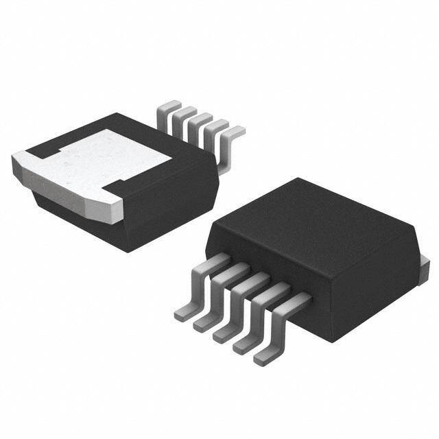
| 产品图片 |
|
| rohs | 符合RoHS无铅 / 符合限制有害物质指令(RoHS)规范要求 |
| 产品系列 | 电源管理 IC,低压差稳压器,ON Semiconductor NCV4274ADS50R4G- |
| 数据手册 | |
| 产品型号 | NCV4274ADS50R4G |
| 产品种类 | 低压差稳压器 |
| 供应商器件封装 | D2PAK |
| 其它名称 | NCV4274ADS50R4GOSCT |
| 包装 | 剪切带 (CT) |
| 商标 | ON Semiconductor |
| 回动电压—最大值 | 500 mV at 250 mA |
| 安装类型 | 表面贴装 |
| 安装风格 | SMD/SMT |
| 封装 | Reel |
| 封装/外壳 | TO-263-4,D²Pak(3 引线+接片),TO-263AA |
| 封装/箱体 | D2PAK |
| 工作温度 | -40°C ~ 150°C |
| 工厂包装数量 | 800 |
| 最大工作温度 | + 150 C |
| 最大输入电压 | 40 V |
| 最小工作温度 | - 40 C |
| 最小输入电压 | 5.5 V |
| 标准包装 | 1 |
| 电压-跌落(典型值) | 0.25V @ 250mA |
| 电压-输入 | 5.5 V ~ 40 V |
| 电压-输出 | 5V |
| 电压调节准确度 | 2 % |
| 电流-输出 | 400mA |
| 电流-限制(最小值) | 400mA |
| 稳压器拓扑 | 正,固定式 |
| 稳压器数 | 1 |
| 系列 | NCV4274 |
| 线路调整率 | 25 mV |
| 负载调节 | 20 mV |
| 输入偏压电流—最大 | 0.19 mA |
| 输出电压 | 5 V |
| 输出电流 | 400 mA |
| 输出端数量 | 1 Output |
| 输出类型 | Fixed |


PDF Datasheet 数据手册内容提取
NCV4274, NCV4274A Regulator Family, 400 mA, 2% and 4% Voltage Description The NCV4274 and NCV4274A is a precision micro−power voltage regulator with an output current capability of 400 mA available in the www.onsemi.com DPAK, D2PAK and SOT−223 packages. The output voltage is accurate within ±2.0% or ±4.0% depending on the version with a maximum dropout voltage of 0.5 V with an input up MARKING DIAGRAMS to 40 V. Low quiescent current is a feature drawing only 150 (cid:2)A with a 4 1 mA load. This part is ideal for automotive and all battery operated microprocessor equipment. 74X−xxG 1 Input The regulator is protected against reverse battery, short circuit, and ALYWW 2, 4 Ground thermal overload conditions. The device can withstand load dump DPAK x 3 Output DT SUFFIX transients making it suitable for use in automotive environments. CASE 369C 2 1 3 Features • 2.5, 3.3 V, 5.0 V, 8.5 V, ±2.0% Output Options 4 • 2.5, 3.3 V, 5.0 V, ±4.0% Output Options • Low 150 (cid:2)A Quiescent Current at 1 mA load current • 1 Input 400 mA Output Current Capability NC 2, 4 Ground • V4274X−xx Fault Protection 3 Output AWLYWWG • D2PAK +60 V Peak Transient Voltage with Respect to GND DS SUFFIX (cid:2) −42 V Reverse Voltage CASE 418AF (cid:2) Short Circuit (cid:2) Thermal Overload 1 2 3 • Very Low Dropout Voltage 4 • NCV Prefix for Automotive and Other Applications Requiring Unique Site and Control Change Requirements; AEC−Q100 AYW 1 Input 74X−xx(cid:3) 2, 4 Ground Qualified and PPAP Capable SOT−223 (cid:3) 3 Output • These are Pb−Free Devices ST SUFFIX CASE 318E 1 2 3 X = A or blank xx = Voltage Ratings A = Assembly Location L, WL = Wafer Lot Y = Year WW, W = Work Week G, (cid:3) = Pb−Free Package (Note: Microdot may be in either location) ORDERING INFORMATION See detailed ordering and shipping information in the package dimensions section on page 15 of this data sheet. © Semiconductor Components Industries, LLC, 2013 1 Publication Order Number: November, 2018 − Rev. 16 NCV4274/D
NCV4274, NCV4274A I Q Bandgap Current Limit and Refernece − Saturation Sense + Thermal Shutdown GND Figure 1. Block Diagram Pin Definitions and Functions Pin No. Symbol Function 1 I Input; Bypass directly at the IC a ceramic capacitor to GND. 2,4 GND Ground 3 Q Output; Bypass with a capacitor to GND. 1. DPAK 3LD package code 6025 2. D2PAK 3LD package code 6083 ABSOLUTE MAXIMUM RATINGS Pin Symbol, Parameter Symbol Condition Min Max Unit I, Input−to−Regulator Voltage VI −42 45 V Current II Internally Internally Limited Limited I, Input peak Transient Voltage to Regulator with Respect VI 60 V to GND Q, Regulated Output Voltage VQ VQ = VI −1.0 40 V Current IQ Internally Internally Limited Limited GND, Ground Current IGND − 100 mA Junction Temperature TJ − 150 °C Storage Temperature TStg −50 150 °C ESD Capability, Human Body Model ESDHB 4 kV ESD Capability, Machine Model ESDMM 200 V ESD Capability, Charged Device Model ESDCDM 1 kV Stresses exceeding those listed in the Maximum Ratings table may damage the device. If any of these limits are exceeded, device functionality should not be assumed, damage may occur and reliability may be affected. 3. This device series incorporates ESD protection and is tested by the following methods: ESD HBM tested per AEC−Q100−002 (EIA/JESD22−A114) ESD MM tested per AEC−Q100−003 (EIA/JESD22−A115) ESD CDM tested per EIA/JES D22/C101, Field Induced Charge Model www.onsemi.com 2
NCV4274, NCV4274A OPERATING RANGE Parameter Symbol Condition Min Max Unit Input Voltage (8.5 V Version) VI 9.0 40 V Input Voltage (5.0 V Version) VI 5.5 40 V Input Voltage (3.3 V, and 2.5 V Version) VI 4.5 40 V Junction Temperature TJ −40 150 °C THERMAL RESISTANCE Parameter Symbol Condition Min Max Unit Junction−to−Ambient DPAK Rthja − 70 °C/W (Note 4) Junction−to−Ambient D2PAK Rthja − 60 °C/W (Note 4) Junction−to−Case DPAK Rthjc − 4 °C/W Junction−to−Case D2PAK Rthjc − 3 °C/W Junction−to−Tab SOT−223 (cid:3)−JLX, − 14.5 °C/W (cid:3)LX (Note 5) Junction−to−Ambient SOT−223 R(cid:4)JA, (cid:4)JA − 169.7 °C/W (Note 5) 4. Soldered in, minimal footprint, FR4 5. 1 oz copper, 5 mm2 copper area, FR4 LEAD FREE SOLDERING TEMPERATURE AND MSL Parameter Symbol Condition Min Max Unit Lead Free Soldering, (Note 6) Tsld 60s − 150s Above 217s °C Reflow (SMD styles only), Pb−Free 40s Max at Peak − 265 pk Moisture Sensitivity Level MSL DPAK and D2PAK 1 − SOT−223 3 − 6. Per IPC/JEDEC J−STD−020C www.onsemi.com 3
NCV4274, NCV4274A ELECTRICAL CHARACTERISTICS −40°C < TJ < 150°C; VI = 13.5 V unless otherwise noted. Min Typ Max Min Typ Max Parameter Symbol Test Conditions NCV4274A NCV4274 Unit REGULATOR Output Voltage (8.5 V Version) VQ 5 mA < IQ < 200 mA 8.33 8.5 8.67 − − − V 9.5 V < VI < 40 V Output Voltage (8.5 V Version) VQ 5 mA < IQ < 400 mA 8.33 8.5 8.67 − − − V 9.5 V < VI < 28 V Output Voltage (5.0 V Version) VQ 5 mA < IQ < 400 mA 4.9 5.0 5.1 4.8 5.0 5.2 V 6 V < VI < 28 V Output Voltage (5.0 V Version) VQ 5 mA < IQ < 200 mA 4.9 5.0 5.1 4.8 5.0 5.2 V 6 V < VI < 40 V Output Voltage (3.3 V Version) VQ 5 mA < IQ < 400 mA 3.23 3.3 3.37 3.17 3.3 3.43 V 4.5 V < VI < 28 V Output Voltage (3.3 V Version) VQ 5 mA < IQ < 200 mA 3.23 3.3 3.37 3.17 3.3 3.43 V 4.5 V < VI < 40 V Output Voltage (2.5 V Version) VQ 5 mA < IQ < 400 mA 2.45 2.5 2.55 2.4 2.5 2.6 V 4.5 V < VI < 28 V Output Voltage (2.5 V Version) VQ 5 mA < IQ < 200 mA 2.45 2.5 2.55 2.4 2.5 2.6 V 4.5 V < VI < 40 V Current Limit IQ − 400 600 − 400 600 − mA Quiescent Current Iq IQ = 1 mA VQ = 8.5 V − 195 250 − − − (cid:2)A VQ = 5.0 V − 190 250 − 190 250 (cid:2)A VQ = 3.3 V − 145 250 − 145 250 (cid:2)A VQ = 2.5 V − 140 250 − 140 250 (cid:2)A IQ = 250 mA VQ = 8.5 V − 10 15 − − − mA VQ = 5.0 V − 10 15 − 10 15 mA VQ = 3.3 V − 13 20 − 13 20 mA VQ = 2.5 V − 12 20 − 12 20 mA IQ = 400 mA VQ = 8.5 V − 20 35 − − − mA VQ = 5.0 V − 20 35 − 20 35 mA VQ = 3.3 V − 30 45 − 30 45 mA VQ = 2.5 V − 28 45 − 28 45 mA Dropout Voltage VDR IQ = 250 mA, VDR = VI − VQ 8.5 V Version VI = 8.5 V − 250 500 − − − mV 5.0 V Version VI = 5.0 V − 250 500 − 250 500 mV 3.3 V Version VI = 4.5 V − − 1.27 − − 1.33 V 2.5 V Version VI = 4.5 V − − 2.05 − − 2.1 V Load Regulation (cid:5)VQ IQ = 5 mA to 400 mA − 7 20 − 7 30 mV Line Regulation (cid:5)VQ (cid:5)VI = 12 V to 32 V − 10 25 − 10 25 mV IQ = 5 mA Power Supply Ripple Rejection PSRR ƒr = 100 Hz, − 60 − − 60 − dB Vr = 0.5 VPP Temperature output voltage drift (cid:5)VQ/(cid:5)T − 0.5 − − 0.5 − mV/K Thermal Shutdown Temperature* TSD IQ = 5 mA 165 − 210 165 − 210 °C *Guaranteed by design, not tested in production www.onsemi.com 4
NCV4274, NCV4274A VI II I 1 NCV4274 3 Q IQ VQ VI 1 NCV4274 3 VQ C11 C12 NCV4274A CQ Input CI NCV4274A CQ* Output VI 1.0 (cid:2)F 100 nF 10 (cid:2)F VQ Rload 100 nF 2,4 or 2,4 22 (cid:2)F GND GND IGND *CQ = 10 (cid:2)F for VQ ≤ 3.3 V CQ = 22 (cid:2)F for VQ ≥ 5 V Figure 2. Measuring Circuit Figure 3. Application Circuit TYPICAL CHARACTERISTIC CURVES 100 1000 VI = 13.5 V VI = 13.5 V 10 100 Maximum ESR COUT = 10 (cid:2)F − 100 (cid:2)F (cid:6)) (cid:6)) Maximum ESR R ( 1 R ( 10 COUT = 1 (cid:2)F − 100 (cid:2)F S S E E Stable Region 0.1 1.0 Stable Region Minimum ESR COUT = 1 (cid:2)F 0.01 0.1 0 50 100 150 200 250 300 350 400 0 5 20 60 100 140 180 220 260 300 340 380 420 LOAD CURRENT (mA) LOAD CURRENT (mA) Figure 4. ESR Characterization − 3.3 V, 5 V and Figure 5. ESR Characterization − 2.5 V Version 8.5 V Versions www.onsemi.com 5
NCV4274, NCV4274A TYPICAL CHARACTERISTIC CURVES − 8.5 V Version 8.7 10 VI = 13.5 V 9 RL = 33 (cid:6) RL = 1.7 k(cid:6) TJ = 25°C 8 8.6 7 6 V) V) (Q 8.5 (Q 5 V V 4 3 8.4 2 1 8.3 0 −40 0 40 80 120 160 0 2 4 6 8 10 TJ (°C) VI (V) Figure 6. Output Voltage vs. Junction Temperature Figure 7. Output Voltage vs. Input Voltage 1000 35 800 TVJQ = = 2 05 °VC 30 VTJI == 1235.°5C V 25 600 A) A) 20 m m I (Q 400 I (q 15 10 200 5 0 0 0 10 20 30 40 50 0 100 200 300 400 500 VI (V) IQ (mA) Figure 8. Output Current vs. Input Voltage Figure 9. Current Consumption vs. Output Current (High Load) 1.6 600 1.4 TJ = 25°C VI = 13.5 V VI = 13.5 V 500 1.2 1 400 TJ = 125°C A) 0.8 mV) 300 I (mq 0.6 V (DR 200 TJ = 25°C 0.4 100 0.2 0 0 0 10 20 30 40 50 60 0 100 200 300 400 IQ (mA) IQ (mA) Figure 10. Current Consumption vs. Output Figure 11. Drop Voltage vs. Output Current Current (Low Load) www.onsemi.com 6
NCV4274, NCV4274A TYPICAL CHARACTERISTIC CURVES − 8.5 V Version 50 6 RL = 33 (cid:6) 4 RL = 6.8 k(cid:6) TJ = 25°C 2 TJ = 25°C 40 0 −2 30 A) A) −4 m m I (q 20 I (I −6 −8 −10 10 −12 −14 0 −16 0 10 20 30 40 50 −50 −30 −10 10 30 50 VI (V) VI (V) Figure 12. Current Consumption vs. Input Voltage Figure 13. Input Current vs. Input Voltage www.onsemi.com 7
NCV4274, NCV4274A TYPICAL CHARACTERISTIC CURVES − 5.0 V Version 5.2 6 VI = 13.5 V RL = 20 (cid:6) RL = 1 k(cid:6) 5 TJ = 25°C 5.1 4 V) V) (Q 5.0 (Q 3 V V 2 4.9 1 4.8 0 −40 0 40 80 120 160 0 2 4 6 8 10 TJ (°C) VI (V) Figure 14. Output Voltage vs. Junction Figure 15. Output Voltage vs. Input Voltage Temperature 800 60 TJ = 25°C TJ = 25°C VQ = 0 V 50 VI = 13.5 V 600 40 A) A) m 400 m 30 (Q (q I I 20 200 10 0 0 0 10 20 30 40 50 0 100 200 300 400 500 600 VI (V) IQ (mA) Figure 16. Output Current vs. Input Voltage Figure 17. Current Consumption vs. Output Current (High Load) 1.6 600 1.4 TJ = 25°C VI = 13.5 V 500 1.2 400 1 TJ = 125°C A) 0.8 mV) 300 I (mq 0.6 V (DR 200 TJ = 25°C 0.4 100 0.2 0 0 0 10 20 30 40 50 60 0 100 200 300 400 IQ (mA) IQ (mA) Figure 18. Current Consumption vs. Output Figure 19. Drop Voltage vs. Output Current Current (Low Load) www.onsemi.com 8
NCV4274, NCV4274A TYPICAL CHARACTERISTIC CURVES − 5.0 V Version 40 6 RTJL == 2250° C(cid:6) 24 TRJL == 265.8°C k(cid:6) 30 0 −2 A) A) −4 m 20 m I (q I (I −6 −8 −10 10 −12 −14 0 −16 0 10 20 30 40 50 −50 −25 0 25 50 VI (V) VI (V) Figure 20. Current Consumption vs. Input Voltage Figure 21. Input Current vs. Input Voltage www.onsemi.com 9
NCV4274, NCV4274A TYPICAL CHARACTERISTIC CURVES − 3.3 V Version 3.5 6 3.4 VRIL = = 6 1 V k(cid:6) 5 RTJL == 2250° C(cid:6) 3.3 4 V) V) (Q 3.2 (Q 3 V V 3.1 2 3.0 1 2.9 0 −40 0 40 80 120 160 0 1 2 3 4 5 6 TJ (°C) VI (V) Figure 22. Output Voltage vs. Junction Figure 23. Output Voltage vs. Input Voltage Temperature 800 60 TJ = 25°C TJ = 25°C VQ = 0 V 50 VI = 13.5 V 600 40 A) A) m 400 m 30 (Q (q I I 20 200 10 0 0 0 10 20 30 40 50 0 100 200 300 400 500 600 VI (V) IQ (mA) Figure 24. Output Current vs. Input Voltage Figure 25. Current Consumption vs. Output Current (High Load) 1.6 1.26 1.4 TJ = 25°C VI = 13.5 V 1.24 1.2 TJ = 125°C 1.22 1.0 I (mA)q 00..68 V (V)DR 1.20 TJ = 25°C 1.18 0.4 VDR = VI(min) − VQ 1.16 0.2 0 1.14 0 10 20 30 40 50 60 0 100 200 300 400 IQ (mA) IQ (mA) Figure 26. Current Consumption vs. Output Figure 27. Voltage Drop vs. Output Current Current (Low Load) www.onsemi.com 10
NCV4274, NCV4274A TYPICAL CHARACTERISTIC CURVES − 3.3 V Version 7 4 6 RL = 20 (cid:6) 2 TJ = 25°C 0 5 −2 A) 4 A) −4 I (mq 3 I (mI −−86 2 −10 −12 RL = 3.3 k(cid:6) 1 −14 TJ = 25°C 0 −16 0 10 20 30 40 50 −50 −25 0 25 50 VI (V) VI (V) Figure 28. Current Consumption vs. Input Voltage Figure 29. Input Current vs. Input Voltage www.onsemi.com 11
NCV4274, NCV4274A TYPICAL CHARACTERISTIC CURVES − 2.5 V Version 2.7 5.0 4.5 2.6 VRIL = = 6 1 V k(cid:6) 4.0 3.5 2.5 3.0 V) V) (Q 2.4 (Q2.5 V V 2.0 2.3 1.5 1.0 2.2 0.5 2.1 0 −40 0 40 80 120 160 0 1 2 3 4 5 6 TJ (°C) VI (V) Figure 30. Output Voltage vs. Junction Figure 31. Output Voltage vs. Input Voltage Temperature 800 60 TVJQ = = 2 05 °VC 50 TVJI == 1235.°5C V 600 40 A) A) m 400 m 30 (Q (q I I 20 200 10 0 0 0 10 20 30 40 50 0 100 200 300 400 500 600 VI (V) IQ (mA) Figure 32. Output Current vs. Input Voltage Figure 33. Current Consumption vs. Output Current (High Load) 1.6 2.05 1.4 TJ = 25°C 2.04 VI = 13.5 V 2.03 1.2 2.02 TJ = 125°C 1.0 2.01 I (mA)q 00..68 V (V)DR 21..0909 TJ = 25°C 1.98 0.4 1.97 VDR = VI(min) − VQ 0.2 1.96 0 1.95 0 10 20 30 40 50 60 0 100 200 300 400 IQ (mA) IQ (mA) Figure 34. Current Consumption vs. Output Figure 35. Voltage Drop vs. Output Current Current (Low Load) www.onsemi.com 12
NCV4274, NCV4274A TYPICAL CHARACTERISTIC CURVES − 2.5 V Version 4.5 2 4.0 RL = 20 (cid:6) TJ = 25°C 0 3.5 −2 3.0 −4 A) 2.5 A) I (mq2.0 I (mI −6 −8 1.5 −10 1.0 0.5 −12 RTJL == 235.3°C k(cid:6) 0 −14 0 10 20 30 40 50 −50 −25 0 25 50 VI (V) VI (V) Figure 36. Current Consumption vs. Input Voltage Figure 37. Input Current vs. Input Voltage www.onsemi.com 13
NCV4274, NCV4274A APPLICATION DESCRIPTION Output Regulator Once the value of P is known, the maximum D(max) The output is controlled by a precision trimmed reference permissible value of R(cid:4)JA can be calculated: and error amplifier. The PNP output has saturation control (cid:7)150C(cid:5)T (cid:8) for regulation while the input voltage is low, preventing over P (cid:4) A (eq. 2) (cid:4) saturation. Current limit and voltage monitors complement JA P D the regulator design to give safe operating signals to the The value of R(cid:4)JA can then be compared with those in the processor and control circuits. package section of the data sheet. Those packages with R(cid:4)JA’s less than the calculated value in Equation 2 will keep Stability Considerations the die temperature below 150°C. In some cases, none of the The input capacitor C in Figure 2 is necessary for I1 packages will be sufficient to dissipate the heat generated by compensating input line reactance. Possible oscillations the IC, and an external heat sink will be required. The current caused by input inductance and input capacitance can be flow and voltages are shown in the Measurement Circuit damped by using a resistor of approximately 1 (cid:6) in series Diagram. with C I2. The output or compensation capacitor helps determine Heat Sinks three main characteristics of a linear regulator: startup delay, A heat sink effectively increases the surface area of the load transient response and loop stability. package to improve the flow of heat away from the IC and The capacitor value and type should be based on cost, into the surrounding air. availability, size and temperature constraints. The Each material in the heat flow path between the IC and the aluminum electrolytic capacitor is the least expensive outside environment will have a thermal resistance. Like solution, but, if the circuit operates at low temperatures series electrical resistances, these resistances are summed to (−25°C to −40°C), both the value and ESR of the capacitor determine the value of R(cid:4)JA: will vary considerably. The capacitor manufacturer’s data sheet usually provides this information. R(cid:4)JA(cid:4)R(cid:4)JC(cid:6)R(cid:4)CS(cid:6)R(cid:4)SA (eq. 3) The value for the output capacitor C shown in Figure 2 Where: Q should work for most applications; however, it is not R(cid:4)JC = the junction−to−case thermal resistance, necessarily the optimized solution. Stability is guaranteed at R(cid:4)CS = the case−to−heat sink thermal resistance, and values CQ (cid:2) 2.2 (cid:2)F and an ESR (cid:3) 2.5 (cid:6) within the R(cid:4)SA = the heat sink−to−ambient thermal resistance. operating temperature range. Actual limits are shown in a R(cid:4)JC appears in the package section of the data sheet. graph in the Typical Performance Characteristics section. Like R(cid:4)JA, it too is a function of package type. R(cid:4)CS and R(cid:4)SA are functions of the package type, heat sink and the Calculating Power Dissipation in a Single Output interface between them. These values appear in data sheets Linear Regulator of heat sink manufacturers. Thermal, mounting, and The maximum power dissipation for a single output heat sinking are discussed in the ON Semiconductor regulator (Figure 3) is: application note AN1040/D, available on the PD(max)(cid:4)[VI(max)(cid:5)VQ(min)]IQ(max)(cid:6)VI(max)Iq (eq. 1) ON Semiconductor Website. Where: V is the maximum input voltage, I(max) V is the minimum output voltage, Q(min) I is the maximum output current for the application, Q(max) and I is the quiescent current the regulator consumes at I . q Q(max) www.onsemi.com 14
NCV4274, NCV4274A ORDERING INFORMATION4 Device* Output Voltage Accuracy Output Voltage Package Shipping† NCV4274ADS85R4G 2% 8.5 V D2PAK 800 / Tape & Reel (Pb−Free) NCV4274DS50G 4% 5.0 V D2PAK 50 Units / Rail (Pb−Free) NCV4274DS50R4G 4% 5.0 V D2PAK 800 / Tape & Reel (Pb−Free) NCV4274DT50RKG 4% 5.0 V DPAK 2500 / Tape & Reel (Pb−Free) NCV4274ADS50G 2% 5.0 V D2PAK 50 Units / Rail (Pb−Free) NCV4274ADS50R4G 2% 5.0 V D2PAK 800 / Tape & Reel (Pb−Free) NCV4274ADT50RKG 2% 5.0 V DPAK 2500 / Tape & Reel (Pb−Free) NCV4274ST33T3G 4% 3.3 V SOT−223 4000 / Tape & Reel (Pb−Free) NCV4274DT33RKG 4% 3.3 V DPAK 2500 / Tape & Reel (Pb−Free) NCV4274AST33T3G 2% 3.3 V SOT−223 4000 / Tape & Reel (Pb−Free) NCV4274ADT33RKG 2% 3.3 V DPAK 2500 / Tape & Reel (Pb−Free) NCV4274ADS33R4G 2% 3.3 V D2PAK 800 / Tape & Reel (Pb−Free) NCV4274ST25T3G 4% 2.5 V SOT−223 4000 / Tape & Reel (Pb−Free) NCV4274AST25T3G 2% 2.5 V SOT−223 4000 / Tape & Reel (Pb−Free) †For information on tape and reel specifications, including part orientation and tape sizes, please refer to our Tape and Reel Packaging Specifications Brochure, BRD8011/D. *NCV Prefix for Automotive and Other Applications Requiring Unique Site and Control Change Requirements; AEC−Q100 Qualified and PPAP Capable. www.onsemi.com 15
MECHANICAL CASE OUTLINE PACKAGE DIMENSIONS SOT−223 (TO−261) CASE 318E−04 ISSUE R SCALE 1:1 DATE 02 OCT 2018 (cid:2) (cid:2) Electronic versions are uncontrolled except when accessed directly from the Document Repository. DOCUMENT NUMBER: 98ASB42680B Printed versions are uncontrolled except when stamped “CONTROLLED COPY” in red. DESCRIPTION: SOT−223 (TO−261) PAGE 1 OF 2 ON Semiconductor and are trademarks of Semiconductor Components Industries, LLC dba ON Semiconductor or its subsidiaries in the United States and/or other countries. ON Semiconductor reserves the right to make changes without further notice to any products herein. ON Semiconductor makes no warranty, representation or guarantee regarding the suitability of its products for any particular purpose, nor does ON Semiconductor assume any liability arising out of the application or use of any product or circuit, and specifically disclaims any and all liability, including without limitation special, consequential or incidental damages. ON Semiconductor does not convey any license under its patent rights nor the rights of others. © Semiconductor Components Industries, LLC, 2018 www.onsemi.com
SOT−223 (TO−261) CASE 318E−04 ISSUE R DATE 02 OCT 2018 STYLE 1: STYLE 2: STYLE 3: STYLE 4: STYLE 5: PIN 1.BASE PIN 1.ANODE PIN 1.GATE PIN 1.SOURCE PIN 1.DRAIN 2.COLLECTOR 2.CATHODE 2.DRAIN 2.DRAIN 2.GATE 3.EMITTER 3.NC 3.SOURCE 3.GATE 3.SOURCE 4.COLLECTOR 4.CATHODE 4.DRAIN 4.DRAIN 4.GATE STYLE 6: STYLE 7: STYLE 8: STYLE 9: STYLE 10: PIN 1.RETURN PIN 1.ANODE 1 CANCELLED PIN 1.INPUT PIN 1.CATHODE 2.INPUT 2.CATHODE 2.GROUND 2.ANODE 3.OUTPUT 3.ANODE 2 3.LOGIC 3.GATE 4.INPUT 4.CATHODE 4.GROUND 4.ANODE STYLE 11: STYLE 12: STYLE 13: PIN 1.MT 1 PIN 1.INPUT PIN 1.GATE 2.MT 2 2.OUTPUT 2.COLLECTOR 3.GATE 3.NC 3.EMITTER 4.MT 2 4.OUTPUT 4.COLLECTOR GENERIC MARKING DIAGRAM* AYW XXXXX(cid:2) (cid:2) 1 A = Assembly Location Y = Year W = Work Week XXXXX = Specific Device Code (cid:2) = Pb−Free Package (Note: Microdot may be in either location) *This information is generic. Please refer to device data sheet for actual part marking. Pb−Free indicator, “G” or microdot “(cid:2)”, may or may not be present. Some products may not follow the Generic Marking. Electronic versions are uncontrolled except when accessed directly from the Document Repository. DOCUMENT NUMBER: 98ASB42680B Printed versions are uncontrolled except when stamped “CONTROLLED COPY” in red. DESCRIPTION: SOT−223 (TO−261) PAGE 2 OF 2 ON Semiconductor and are trademarks of Semiconductor Components Industries, LLC dba ON Semiconductor or its subsidiaries in the United States and/or other countries. ON Semiconductor reserves the right to make changes without further notice to any products herein. ON Semiconductor makes no warranty, representation or guarantee regarding the suitability of its products for any particular purpose, nor does ON Semiconductor assume any liability arising out of the application or use of any product or circuit, and specifically disclaims any and all liability, including without limitation special, consequential or incidental damages. ON Semiconductor does not convey any license under its patent rights nor the rights of others. © Semiconductor Components Industries, LLC, 2018 www.onsemi.com
MECHANICAL CASE OUTLINE PACKAGE DIMENSIONS 4 DPAK (SINGLE GAUGE) CASE 369C ISSUE F 1 2 DATE 21 JUL 2015 3 SCALE 1:1 NOTES: A 1.DIMENSIONING AND TOLERANCING PER ASME Y14.5M, 1994. E C 2.CONTROLLING DIMENSION: INCHES. A 3.THERMAL PAD CONTOUR OPTIONAL WITHIN DI- b3 B MENSIONS b3, L3 and Z. c2 4.DIMENSIONS D AND E DO NOT INCLUDE MOLD FLASH, PROTRUSIONS, OR BURRS. MOLD FLASH, PROTRUSIONS, OR GATE BURRS SHALL 4 NOT EXCEED 0.006 INCHES PER SIDE. L3 Z 5.DIMENSIONS D AND E ARE DETERMINED AT THE D DETAIL A H 6.DOAUTTUEMRSM OA SATN EDX BT RAERME EDSE OTEFR TMHIEN EPDLA ASTT DICA TBUOMDY. 1 2 3 PLANE H. 7.OPTIONAL MOLD FEATURE. L4 INCHES MILLIMETERS NOTE 7 b2 c BOTTOM VIEW DIM MIN MAX MIN MAX A 0.086 0.094 2.18 2.38 e SIDE VIEW A1 0.000 0.005 0.00 0.13 b b 0.025 0.035 0.63 0.89 0.005 (0.13) M C b2 0.028 0.045 0.72 1.14 TOP VIEW b3 0.180 0.215 4.57 5.46 c 0.018 0.024 0.46 0.61 c2 0.018 0.024 0.46 0.61 H Z Z D 0.235 0.245 5.97 6.22 E 0.250 0.265 6.35 6.73 e 0.090 BSC 2.29 BSC L2 GPLAAUNGEE C SPELAATNIENG H 0.370 0.410 9.40 10.41 L 0.055 0.070 1.40 1.78 L1 0.114 REF 2.90 REF L2 0.020 BSC 0.51 BSC L A1 BOTTOM VIEW L3 0.035 0.050 0.89 1.27 L1 ALTERNATE L4 −−− 0.040 −−− 1.01 CONSTRUCTIONS Z 0.155 −−− 3.93 −−− DETAIL A ROTATED 90(cid:2) CW GENERIC MARKING DIAGRAM* STYLE 1: STYLE 2: STYLE 3: STYLE 4: STYLE 5: PIN 1.BASE PIN 1.GATE PIN 1.ANODE PIN 1.CATHODE PIN 1.GATE 2.COLLECTOR 2.DRAIN 2.CATHODE 2.ANODE 2.ANODE 3.EMITTER 3.SOURCE 3.ANODE 3.GATE 3.CATHODE 4.COLLECTOR 4.DRAIN 4.CATHODE 4.ANODE 4.ANODE XXXXXXG AYWW ALYWW XXX STYLE 6: STYLE 7: STYLE 8: STYLE 9: STYLE 10: XXXXXG PIN 1.MT1 PIN 1.GATE PIN 1.N/C PIN 1.ANODE PIN 1.CATHODE 2.MT2 2.COLLECTOR 2.CATHODE 2.CATHODE 2.ANODE 3.GATE 3.EMITTER 3.ANODE 3.RESISTOR ADJUST 3.CATHODE 4.MT2 4.COLLECTOR 4.CATHODE 4.CATHODE 4.ANODE IC Discrete SOLDERING FOOTPRINT* XXXXXX = Device Code A = Assembly Location 6.20 3.00 L = Wafer Lot 0.244 0.118 2.58 Y = Year 0.102 WW = Work Week G = Pb−Free Package *This information is generic. Please refer 5.80 1.60 6.17 to device data sheet for actual part 0.228 0.063 0.243 marking. (cid:2) (cid:3) mm SCALE 3:1 inches *For additional information on our Pb−Free strategy and soldering details, please download the ON Semiconductor Soldering and Mounting Techniques Reference Manual, SOLDERRM/D. DOCUMENT NUMBER: 98AON10527D Electronic versions are uncontrolled except when accessed directly from the Document Repository. Printed STATUS: ON SEMICONDUCTOR STANDARD versions are uncontrolled except when stamped “CONTROLLED COPY” in red. NEW STANDARD: REF TO JEDEC TO−252 © Semiconductor Components Industries, LLC, 2002 http://onsemi.com Case Outline Number: October, D20E0S2C −R RIePvT. I0ON: DPAK SINGLE GAUGE SURFA1CE MOUNT PAGE 1 OFX 2XX
DOCUMENT NUMBER: 98AON10527D PAGE 2 OF 2 ISSUE REVISION DATE O RELEASED FOR PRODUCTION. REQ. BY L. GAN 24 SEP 2001 A ADDED STYLE 8. REQ. BY S. ALLEN. 06 AUG 2008 B ADDED STYLE 9. REQ. BY D. WARNER. 16 JAN 2009 C ADDED STYLE 10. REQ. BY S. ALLEN. 09 JUN 2009 D RELABELED DRAWING TO JEDEC STANDARDS. ADDED SIDE VIEW DETAIL A. 29 JUN 2010 CORRECTED MARKING INFORMATION. REQ. BY D. TRUHITTE. E ADDED ALTERNATE CONSTRUCTION BOTTOM VIEW. MODIFIED DIMENSIONS 06 FEB 2014 b2 AND L1. CORRECTED MARKING DIAGRAM FOR DISCRETE. REQ. BY I. CAM- BALIZA. F ADDED SECOND ALTERNATE CONSTRUCTION BOTTOM VIEW. REQ. BY K. 21 JUL 2015 MUSTAFA. ON Semiconductor and are registered trademarks of Semiconductor Components Industries, LLC (SCILLC). SCILLC reserves the right to make changes without further notice to any products herein. SCILLC makes no warranty, representation or guarantee regarding the suitability of its products for any particular purpose, nor does SCILLC assume any liability arising out of the application or use of any product or circuit, and specifically disclaims any and all liability, including without limitation special, consequential or incidental damages. “Typical” parameters which may be provided in SCILLC data sheets and/or specifications can and do vary in different applications and actual performance may vary over time. All operating parameters, including “Typicals” must be validated for each customer application by customer’s technical experts. SCILLC does not convey any license under its patent rights nor the rights of others. SCILLC products are not designed, intended, or authorized for use as components in systems intended for surgical implant into the body, or other applications intended to support or sustain life, or for any other application in which the failure of the SCILLC product could create a situation where personal injury or death may occur. Should Buyer purchase or use SCILLC products for any such unintended or unauthorized application, Buyer shall indemnify and hold SCILLC and its officers, employees, subsidiaries, affiliates, and distributors harmless against all claims, costs, damages, and expenses, and reasonable attorney fees arising out of, directly or indirectly, any claim of personal injury or death associated with such unintended or unauthorized use, even if such claim alleges that SCILLC was negligent regarding the design or manufacture of the part. SCILLC is an Equal Opportunity/Affirmative Action Employer. This literature is subject to all applicable copyright laws and is not for resale in any manner. © Semiconductor Components Industries, LLC, 2015 Case Outline Number: July, 2015 − Rev. F 369C
MECHANICAL CASE OUTLINE PACKAGE DIMENSIONS D2PAK CASE 418AF ISSUE E DATE 15 SEP 2015 SCALE 1:1 NOTES: T T 1. DIMENSIONING AND TOLERANCING PER ANSI TERMINAL 4 Y14.5M, 1982. K A OCHPATIMOFNCEARL ED U OCHPATIMOFNCEARL ES 23.. CTAA OABNN CTDRO KON.LTLOINUGR ODIPMTEIONNSAIOLN W: IINTHCIHNE DSI.MENSIONS 4. DIMENSIONS U AND V ESTABLISH A MINIMUM S MOUNTING SURFACE FOR TERMINAL 4. V 5. DIMENSIONS A AND B DO NOT INCLUDE MOLD B FLASH OR GATE PROTRUSIONS. MOLD FLASH H DETAIL C DETAIL C AND GATE PROTRUSIONS NOT TO EXCEED 1 2 3 0.025 (0.635) MAXIMUM. 6. SINGLE GAUGE DESIGN WILL BE SHIPPED AF TER FPCN EXPIRATION IN OCTOBER 2011. J INCHES MILLIMETERS F SIDE VIEW BOTTOM VIEW SIDE VIEW DIM MIN MAX MIN MAX G DUAL GAUGE SINGLE GAUGE A 0.386 0.403 9.804 10.236 3XD CONSTRUCTION CONSTRUCTION BC 00..315760 00..316880 94..034128 94..354772 0.010 (0.254) M T D 0.026 0.036 0.660 0.914 TOP VIEW ED 0.045 0.055 1.143 1.397 ES 0.018 0.026 0.457 0.660 F 0.051 REF 1.295 REF G 0.100 BSC 2.540 BSC H 0.539 0.579 13.691 14.707 N T J 0.125 MAX 3.175 MAX M K 0.050 REF 1.270 REF L 0.000 0.010 0.000 0.254 M 0.088 0.102 2.235 2.591 SEATING N 0.018 0.026 0.457 0.660 P L PLANE P 0.058 0.078 1.473 1.981 R 0(cid:2) 8(cid:2) 0(cid:2) 8(cid:2) R DETAIL C BOTTOM VIEW S 0.116 REF 2.946 REF OPTIONAL CONSTRUCTIONS U 0.200 MIN 5.080 MIN V 0.250 MIN 6.350 MIN SOLDERING FOOTPRINT* GENERIC 10.490 MARKING DIAGRAM* 8.380 XX XXXXXXXXX AWLYYWWG 16.155 3X 3.504 XXXXX = Specific Device Code A = Assembly Location 3X1.016 WL = Wafer Lot YY = Year 2.540 WW = Work Week PITCH DIMENSIONS: MILLIMETERS G = Pb−Free Package *For additional information on our Pb−Free strategy and soldering *This information is generic. Please refer details, please download the ON Semiconductor Soldering and to device data sheet for actual part Mounting Techniques Reference Manual, SOLDERRM/D. marking. Pb−Free indicator, “G”, may or not be present. Electronic versions are uncontrolled except when accessed directly from the Document Repository. DOCUMENT NUMBER: 98AON21981D Printed versions are uncontrolled except when stamped “CONTROLLED COPY” in red. DESCRIPTION: D2PAK PAGE 1 OF 1 ON Semiconductor and are trademarks of Semiconductor Components Industries, LLC dba ON Semiconductor or its subsidiaries in the United States and/or other countries. ON Semiconductor reserves the right to make changes without further notice to any products herein. ON Semiconductor makes no warranty, representation or guarantee regarding the suitability of its products for any particular purpose, nor does ON Semiconductor assume any liability arising out of the application or use of any product or circuit, and specifically disclaims any and all liability, including without limitation special, consequential or incidental damages. ON Semiconductor does not convey any license under its patent rights nor the rights of others. © Semiconductor Components Industries, LLC, 2018 www.onsemi.com
ON Semiconductor and are trademarks of Semiconductor Components Industries, LLC dba ON Semiconductor or its subsidiaries in the United States and/or other countries. ON Semiconductor owns the rights to a number of patents, trademarks, copyrights, trade secrets, and other intellectual property. A listing of ON Semiconductor’s product/patent coverage may be accessed at www.onsemi.com/site/pdf/Patent−Marking.pdf. ON Semiconductor reserves the right to make changes without further notice to any products herein. ON Semiconductor makes no warranty, representation or guarantee regarding the suitability of its products for any particular purpose, nor does ON Semiconductor assume any liability arising out of the application or use of any product or circuit, and specifically disclaims any and all liability, including without limitation special, consequential or incidental damages. Buyer is responsible for its products and applications using ON Semiconductor products, including compliance with all laws, regulations and safety requirements or standards, regardless of any support or applications information provided by ON Semiconductor. “Typical” parameters which may be provided in ON Semiconductor data sheets and/or specifications can and do vary in different applications and actual performance may vary over time. All operating parameters, including “Typicals” must be validated for each customer application by customer’s technical experts. ON Semiconductor does not convey any license under its patent rights nor the rights of others. ON Semiconductor products are not designed, intended, or authorized for use as a critical component in life support systems or any FDA Class 3 medical devices or medical devices with a same or similar classification in a foreign jurisdiction or any devices intended for implantation in the human body. Should Buyer purchase or use ON Semiconductor products for any such unintended or unauthorized application, Buyer shall indemnify and hold ON Semiconductor and its officers, employees, subsidiaries, affiliates, and distributors harmless against all claims, costs, damages, and expenses, and reasonable attorney fees arising out of, directly or indirectly, any claim of personal injury or death associated with such unintended or unauthorized use, even if such claim alleges that ON Semiconductor was negligent regarding the design or manufacture of the part. ON Semiconductor is an Equal Opportunity/Affirmative Action Employer. This literature is subject to all applicable copyright laws and is not for resale in any manner. PUBLICATION ORDERING INFORMATION LITERATURE FULFILLMENT: N. American Technical Support: 800−282−9855 Toll Free ON Semiconductor Website: www.onsemi.com Literature Distribution Center for ON Semiconductor USA/Canada 19521 E. 32nd Pkwy, Aurora, Colorado 80011 USA Europe, Middle East and Africa Technical Support: Order Literature: http://www.onsemi.com/orderlit Phone: 303−675−2175 or 800−344−3860 Toll Free USA/Canada Phone: 421 33 790 2910 Fax: 303−675−2176 or 800−344−3867 Toll Free USA/Canada For additional information, please contact your local Email: orderlit@onsemi.com Sales Representative ◊
Mouser Electronics Authorized Distributor Click to View Pricing, Inventory, Delivery & Lifecycle Information: O N Semiconductor: NCV4274ADS85R4G NCV4274ADS33R4G NCV4274ADT50RKG NCV4274AST33T3G NCV4274AST25T3G NCV4274ADT33RKG NCV4274ADS50R4G