ICGOO在线商城 > BA10T
 Datasheet下载
- 型号: BA10T
- 制造商: ROHM Semiconductor
- 库位|库存: xxxx|xxxx
- 要求:
| 数量阶梯 | 香港交货 | 国内含税 |
| +xxxx | $xxxx | ¥xxxx |
查看当月历史价格
查看今年历史价格
BA10T产品简介:
ICGOO电子元器件商城为您提供BA10T由ROHM Semiconductor设计生产,在icgoo商城现货销售,并且可以通过原厂、代理商等渠道进行代购。 提供BA10T价格参考¥18.03-¥20.40以及ROHM SemiconductorBA10T封装/规格参数等产品信息。 你可以下载BA10T参考资料、Datasheet数据手册功能说明书, 资料中有BA10T详细功能的应用电路图电压和使用方法及教程。
| 参数 | 数值 |
| 产品目录 | 集成电路 (IC)半导体 |
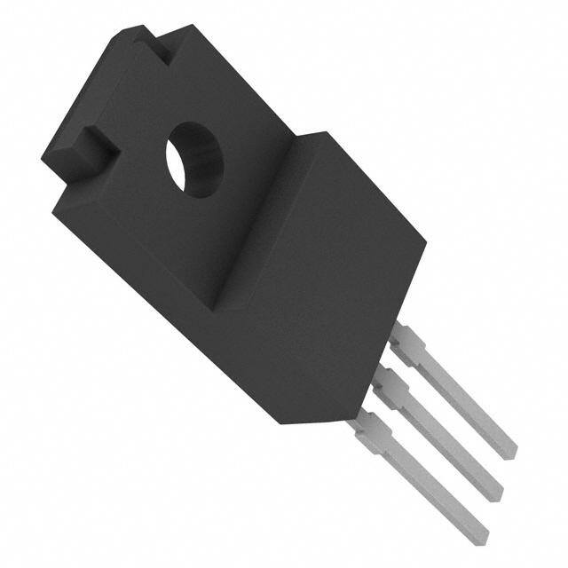
| 描述 | IC REG LDO 10V 1A TO220FP低压差稳压器 REGULATOR 10V 1A |
| 产品分类 | |
| 品牌 | ROHM Semiconductor |
| 产品手册 | |
| 产品图片 |
|
| rohs | 符合RoHS无铅 / 符合限制有害物质指令(RoHS)规范要求 |
| 产品系列 | 电源管理 IC,低压差稳压器,ROHM Semiconductor BA10T- |
| 数据手册 | |
| 产品型号 | BA10T |
| 产品培训模块 | http://www.digikey.cn/PTM/IndividualPTM.page?site=cn&lang=zhs&ptm=30333 |
| 产品种类 | 低压差稳压器 |
| 供应商器件封装 | TO-220FP |
| 包装 | 散装 |
| 商标 | ROHM Semiconductor |
| 回动电压—最大值 | 500 mV |
| 安装类型 | 通孔 |
| 安装风格 | Through Hole |
| 封装 | Bulk |
| 封装/外壳 | TO-220-3 整包 |
| 封装/箱体 | TO-220-3 FP |
| 工作温度 | -40°C ~ 85°C |
| 工厂包装数量 | 500 |
| 最大功率耗散 | 2 W |
| 最大工作温度 | + 85 C |
| 最大输入电压 | 25 V |
| 最小工作温度 | - 40 C |
| 最小输入电压 | 11 V |
| 标准包装 | 500 |
| 特色产品 | http://www.digikey.cn/product-highlights/cn/zh/rohm-ba-bd-ldo-regulator-ics/3995 |
| 电压-跌落(典型值) | 0.3V @ 500mA |
| 电压-输入 | 11 V ~ 25 V |
| 电压-输出 | 10V |
| 电流-输出 | 1A |
| 电流-限制(最小值) | - |
| 稳压器拓扑 | 正,固定式 |
| 稳压器数 | 1 |
| 线路调整率 | 100 mV |
| 负载调节 | 150 mV |
| 输出电压 | 10 V |
| 输出电流 | 1 A |
| 输出端数量 | 1 Output |
| 输出类型 | Fixed |


- 商务部:美国ITC正式对集成电路等产品启动337调查
- 曝三星4nm工艺存在良率问题 高通将骁龙8 Gen1或转产台积电
- 太阳诱电将投资9.5亿元在常州建新厂生产MLCC 预计2023年完工
- 英特尔发布欧洲新工厂建设计划 深化IDM 2.0 战略
- 台积电先进制程称霸业界 有大客户加持明年业绩稳了
- 达到5530亿美元!SIA预计今年全球半导体销售额将创下新高
- 英特尔拟将自动驾驶子公司Mobileye上市 估值或超500亿美元
- 三星加码芯片和SET,合并消费电子和移动部门,撤换高东真等 CEO
- 三星电子宣布重大人事变动 还合并消费电子和移动部门
- 海关总署:前11个月进口集成电路产品价值2.52万亿元 增长14.8%


PDF Datasheet 数据手册内容提取
BAOOT / FP series Regulator ICs Low saturation voltage type 3-pin regulator BAOOT / FP series The BAΟΟT/ FP series are fixed positive output low drop-out type, 3-pin voltage regulators with positive output.. These regulators are used to provide a stabilized output voltage from a fluctuating DC input voltage. There are 10 fixed output voltages, as follows:3V, 3.3V, 5V, 6V*, 7V, 8V, 9V, 10V, 12V and 15V. The maximum current capacity is 1A for each of the above voltages. (Items marked with an asterisk are under development.) !!!!Applications Constant voltage power supply !!!!Features 1) Built-in overvoltage protection circuit, overcurrent 3) Compatible with the BA178ΟΟ series. protection circuit and thermal shutdown circuit. 4) Richly diverse lineup. 2) TO220FP and TO252-3 packages are available to 5) Low minimum I / O voltage differential. cover a wide range of applications. !!!!Product codes Output voltage (V) Product No. Output voltage (V) Product No. 3.0 BA03T / FP 8.0 BA08T / FP 3.3 BA033T / FP 9.0 BA09T / FP 5.0 BA05T / FP 10.0 BA10T / FP 6.0 BA06T * / FP* 12.0 BA12T / FP 7.0 BA07T / FP 15.0 BA15T / FP * : Under development. !!!!Block diagram VCC 1 REFERENCE − VOLTAGE OUT + 3 + GND 2
BAOOT / FP series Regulator ICs !!!!Absolute maximum ratings (Ta = 25°C) Parameter Symbol Limits Unit Power supply voltage VCC 35 V Power TO220FP 2000 *1 Pd mW dissipation TO252 - 3 1000 *2 Operating temperature Topr -40~85 °C Storage temperature Tstg -55~150 °C Peak applied voltage Vsurge 50 *3 V *1 Reduced by 16mW for each increase in Ta of 1°C over 25°C *2 Reduced by 8mW for each increase in Ta of 1°C over 25°C *3 Voltage application time : 200 msec. or less !!!!Recommended operating conditions BA03T / FP BA08T / FP Parameter Symbol Min. Typ. Max. Unit Parameter Symbol Min. Typ. Max. Unit Input voltage VIN 4 - 25 V Input voltage VIN 9 - 25 V Output current Io - - 1 A Output current Io - - 1 A BA033T / FP BA09T / FP Parameter Symbol Min. Typ. Max. Unit Parameter Symbol Min. Typ. Max. Unit Input voltage VIN 4.3 - 25 V Input voltage VIN 10 - 25 V Output current Io - - 1 A Output current Io - - 1 A BA05T / FP BA10T / FP Parameter Symbol Min. Typ. Max. Unit Parameter Symbol Min. Typ. Max. Unit Input voltage VIN 6 - 25 V Input voltage VIN 11 - 25 V Output current Io - - 1 A Output current Io - - 1 A BA06T / FP (under development) BA12T / FP Parameter Symbol Min. Typ. Max. Unit Parameter Symbol Min. Typ. Max. Unit Input voltage VIN 7 - 25 V Input voltage VIN 13 - 25 V Output current Io - - 1 A Output current Io - - 1 A BA07T / FP BA15T / FP Parameter Symbol Min. Typ. Max. Unit Parameter Symbol Min. Typ. Max. Unit Input voltage VIN 8 - 25 V Input voltage VIN 16 - 25 V Output current Io - - 1 A Output current Io - - 1 A
BAOOT / FP series Regulator ICs !!!!Electrical characteristics BA03T / FP (unless otherwise noted, Ta = 25°C, VCC = 8V, IO = 500mA) Measurement Parameter Symbol Min. Typ. Max. Unit Conditions circuit Output voltage VO1 2.85 3.0 3.15 V - Fig.1 Input stability Reg.I - 20 100 mV VIN = 4→25V Fig.1 Ripple rejection ratio R.R. 45 55 - dB eIN = 1Vrms, f = 120Hz, Io = 100mA Fig.2 Load regulation Reg.L - 50 150 mV Io = 5mA→1A Fig.1 Temperature coefficient of output voltage Tcvo - ±0.02 - % / °C Io = 5mA, Tj = 0~125°C Fig.1 Dropout voltage Vd - 0.3 0.5 V Vcc = 0.95VO Fig.3 Bias current Ib - 2.5 5.0 mA Io = 0mA Fig.4 Peak output current IO-P 1.0 1.5 - A Tj = 25°C Fig.1 Output short-circuit current Ios - 0.4 - A Vcc = 25V Fig.5 BA033T / FP (unless otherwise noted, Ta = 25°C, VCC = 8V, IO = 500mA) Measurement Parameter Symbol Min. Typ. Max. Unit Conditions circuit Output voltage VO1 3.13 3.3 3.47 V - Fig.1 Input stability Reg.I - 20 100 mV VIN = 4.3→25V Fig.1 Ripple rejection ratio R.R. 45 55 - dB eIN = 1Vrms, f = 120Hz, Io = 100mA Fig.2 Load regulation Reg.L - 50 150 mV Io = 5mA→1A Fig.1 Temperature coefficient of output voltage Tcvo - ±0.02 - % / °C Io = 5mA, Tj = 0~125°C Fig.1 Dropout voltage Vd - 0.3 0.5 V Vcc = 0.95VO Fig.3 Bias current Ib - 2.5 5.0 mA Io = 0mA Fig.4 Peak output current IO-P 1.0 1.5 - A Tj = 25°C Fig.1 Output short-circuit current Ios - 0.4 - A Vcc = 25V Fig.5 BA05T / FP (unless otherwise noted, Ta = 25°C, VCC = 10V, IO = 500mA) Measurement Parameter Symbol Min. Typ. Max. Unit Conditions circuit Output voltage VO1 4.75 5.0 5.25 V - Fig.1 Input stability Reg.I - 20 100 mV VIN = 6→25V Fig.1 Ripple rejection ratio R.R. 45 55 - dB eIN = 1Vrms, f = 120Hz, Io = 100mA Fig.2 Load regulation Reg.L - 50 150 mV Io = 5mA→1A Fig.1 Temperature coefficient of output voltage Tcvo - ±0.02 - % / °C Io = 5mA, Tj = 0~125°C Fig.1 Dropout voltage Vd - 0.3 0.5 V Vcc = 4.75V Fig.3 Bias current Ib - 2.5 5.0 mA Io = 0mA Fig.4 Peak output current IO-P 1.0 1.5 - A Tj = 25°C Fig.1 Output short-circuit current Ios - 0.4 - A Vcc = 25V Fig.5
BAOOT / FP series Regulator ICs BA06T / FP (unless otherwise noted, Ta = 25°C, VCC = 11V, IO = 500mA) (under development) Measurement Parameter Symbol Min. Typ. Max. Unit Conditions circuit Output voltage VO1 5.7 6.0 6.3 V - Fig.1 Input stability Reg.I - 20 100 mV VIN = 7→25V Fig.1 Ripple rejection ratio R.R. 45 55 - dB eIN = 1Vrms, f = 120Hz, Io = 100mA Fig.2 Load regulation Reg.L - 50 150 mV Io = 5mA→1A Fig.1 Temperature coefficient of output voltage Tcvo - ±0.02 - % / °C Io = 5mA, Tj = 0125°C Fig.1 Dropout voltage Vd - 0.3 0.5 V Vcc = 0.95V Fig.3 Bias current Ib - 2.5 5.0 mA Io = 0mA Fig.4 Peak output current IO-P 1.0 1.5 - A Tj = 25°C Fig.1 Output short-circuit current Ios - 0.4 - A Vcc = 25V Fig.5 BA07T / FP (unless otherwise noted, Ta = 25°C, VCC = 12V, IO = 500mA) Measurement Parameter Symbol Min. Typ. Max. Unit Conditions circuit Output voltage VO1 6.65 7.0 7.35 V - Fig.1 Input stability Reg.I - 20 100 mV VIN = 8→25V Fig.1 Ripple rejection ratio R.R. 45 55 - dB eIN = 1Vrms, f = 120Hz, Io = 100mA Fig.2 Load regulation Reg.L - 50 150 mV Io = 5mA→1A Fig.1 Temperature coefficient of output voltage Tcvo - ±0.02 - % / °C Io = 5mA, Tj = 0~125°C Fig.1 Dropout voltage Vd - 0.3 0.5 V Vcc = 0.95VO Fig.3 Bias current Ib - 2.5 5.0 mA Io = 0mA Fig.4 Peak output current IO-P 1.0 1.5 - A Tj = 25°C Fig.1 Output short-circuit current Ios - 0.4 - A Vcc = 25V Fig.5 BA08T / FP (unless otherwise noted, Ta = 25°C, VCC = 13V, IO = 500mA) Measurement Parameter Symbol Min. Typ. Max. Unit Conditions Circuit Output voltage VO1 7.6 8.0 8.4 V - Fig.1 Input stability Reg.I - 20 100 mV VIN = 9→25V Fig.1 Ripple rejection ratio R.R. 45 55 - dB eIN = 1Vrms, f = 120Hz, Io = 100mA Fig.2 Load regulation Reg.L - 50 150 mV Io = 5mA→1A Fig.1 Temperature coefficient of output voltage Tcvo - ±0.02 - % / °C Io = 5mA, Tj = 0~125°C Fig.1 Dropout voltage Vd - 0.3 0.5 V Vcc = 0.95VO Fig.3 Bias current Ib - 2.5 5.0 mA Io = 0mA Fig.4 Peak output current IO-P 1.0 1.5 - A Tj = 25°C Fig.1 Output short-circuit current Ios - 0.4 - A Vcc = 25V Fig.5
BAOOT / FP series Regulator ICs BA09T / FP (unless otherwise noted, Ta = 25°C, VCC = 14V, IO = 500mA) (under development) Measurement Parameter Symbol Min. Typ. Max. Unit Conditions circuit Output voltage VO1 8.45 9.0 9.45 V - Fig.1 Input stability Reg.I - 20 100 mV VIN = 10→25V Fig.1 Ripple rejection ratio R.R. 45 55 - dB eIN = 1Vrms, f = 120Hz, Io = 100mA Fig.2 Load regulation Reg.L - 50 150 mV Io = 5mA→1A Fig.1 Temperature coefficient of output voltage Tcvo - ±0.02 - % / °C Io = 5mA, Tj = 0~125°C Fig.1 Dropout voltage Vd - 0.3 0.5 V Vcc = 0.95VO Fig.3 Bias current Ib - 2.5 5.0 mA Io = 0mA Fig.4 Peak output current IO-P 1.0 1.5 - A Tj = 25°C Fig.1 Output short-circuit current Ios - 0.4 - A Vcc = 25V Fig.5 BA10T / FP (unless otherwise noted, Ta = 25°C, VCC = 15V, IO = 500mA) Measurement Parameter Symbol Min. Typ. Max. Unit Conditions circuit Output voltage VO1 9.5 10 10.5 V - Fig.1 Input stability Reg.I - 20 100 mV VIN = 11→25V Fig.1 Ripple rejection ratio R.R. 45 55 - dB eIN = 1Vrms, f = 120Hz, Io = 100mA Fig.2 Load regulation Reg.L - 50 150 mV Io = 5mA→1A Fig.1 Temperature coefficient of output voltage Tcvo - ±0.02 - % / °C Io = 5mA, Tj = 0~125°C Fig.1 Dropout voltage Vd - 0.3 0.5 V Vcc = 0.95VO Fig.3 Bias current Ib - 2.5 5.0 mA Io = 0mA Fig.4 Peak output current IO-P 1.0 1.5 - A Tj = 25°C Fig.1 Output short-circuit current Ios - 0.4 - A Vcc = 25V Fig.5 BA12T / FP (unless otherwise noted, Ta = 25°C, VCC = 17V, IO = 500mA) Measurement Parameter Symbol Min. Typ. Max. Unit Conditions circuit Output voltage VO1 11.4 12 12.6 V - Fig.1 Input stability Reg.I - 20 100 mV VIN = 13→25V Fig.1 Ripple rejection ratio R.R. 45 55 - dB eIN = 1Vrms, f = 120Hz, Io = 100mA Fig.2 Load regulation Reg.L - 50 150 mV Io = 5mA→1A Fig.1 Temperature coefficient of output voltage Tcvo - ±0.02 - % / °C Io = 5mA, Tj = 0~125°C Fig.1 Dropout voltage Vd - 0.3 0.5 V Vcc = 0.95VO Fig.3 Bias current Ib - 2.5 5.0 mA Io = 0mA Fig.4 Peak output current IO-P 1.0 1.5 - A Tj = 25°C Fig.1 Output short-circuit current Ios - 0.4 - A Vcc = 25V Fig.5
BAOOT / FP series Regulator ICs BA15T / FP (unless otherwise noted, Ta = 25°C, VCC = 20V, IO = 500mA) Measurement Parameter Symbol Min. Typ. Max. Unit Conditions circuit Output voltage VO1 14.25 15 15.75 V - Fig.1 Input stability Reg.I - 20 100 mV VIN = 6→25V Fig.1 Ripple rejection ratio R.R. 45 55 - dB eIN = 1Vrms, f = 120Hz, Io = 100mA Fig.2 Load regulation Reg.L - 90 200 mV Io = 5mA→1A Fig.1 Temperature coefficient of output voltage Tcvo - ±0.02 - % / °C Io = 5mA, Tj = 0~125°C Fig.1 Dropout voltage Vd - 0.3 0.5 V Vcc = 0.95VO Fig.3 Bias current Ib - 2.5 5.0 mA Io = 0mA Fig.4 Peak output current IO-P 1.0 1.5 - A Tj = 25°C Fig.1 Output short-circuit current Ios - 0.4 - A Vcc = 30V Fig.5
BAOOT / FP series Regulator ICs !!!!Measurement circuits V ein 10Ω5W VCC µ0.33F VCC GNDOUT 22µFIO V VCC 1000.3µ3FµF VCC GNDOUT 22µF VeOUT IO = 100mA eIN = 1Vrms f = 120Hz Ripple rejection ratio R.R. = 20 log( eIN ) eOUT Fig. 1 Measurement circuit for output voltage, Fig. 2 Measurement circuit for ripple rejection ratio input stability, load regulation, temperature coefficient of output voltage V 0.33µF VCC OUT 22µF VCC GND VCC OUT 0.33µF 22µF VCC = 0.95VO GND IO = 500mA A Fig. 3 Measurement circuit for minimum I/O voltage differential Fig. 4 Measurement circuit for bias current 0.33µF VCC OUT 22µF VCC GND IOS A Fig. 5 Measurement circuit for output short-circuit current
BAOOT / FP series Regulator ICs !!!!Operation notes (1) Operating power supply voltage shorted. When operating within the normal voltage range and This protection circuit limits the current in the shape of within the ambient operating temperature range, most a ’7’. This circuit is designed with a high margin, so that circuit functions are guaranteed. that current is restricted and latching is prevented, even if The rated values cannot be guaranteed for the electrical a high-capacitance capacitator causes a large amount of characteristics, but there are no sudden changes of the current to temporary flow through the IC. characteristics within these ranges. However, these protection circuits are only good for pre- (2) Power dissipation venting damage from sudden accidents and should not Heat attenuation characteristics are noted on a separate be used for continuous protection (for instance, clamping page and can be used as a guide in judging power at an output of 1VF or greater; below 1VF , the short mode dissipation. circuit operates). Note that the capacitor has negative If these ICs are used in such a way that the allowable temperature characteristics, and the design should take power dissipation level is exceeded, an increase in the this into consideration. chip temperature could cause a reduction in the current (5) Thermal overload circuit capability or could otherwise adversely affect the A built-in thermal overload circuit prevents damage from performance of the IC. Make sure a sufficient margin is overheating. When the thermal circuit is activated, the allowed so that the allowable power dissipation value is outputs are turned OFF. When the temperature drops not exceeded. back to a constant level, the circuit is restored. (3) Output oscillation prevention and bypass capacitor (6) Internal circuits could be damaged if there are Be sure to connect a capacitor between the output pin modes in which the electric potential of the application’s and GND to prevent oscillation. Since fluctuations in the input (VCC ) and GND are the opposite of the electric valve of the capacitor due to temperature changes may potential normally used by each of the outputs. Use of a cause oscillations, a tantalum electrolytic capacitor with a diode or other such bypass path is recommended. small internal series resistance (ESR) is recommended. (7) Although the manufacture of this product includes A 22µ F capacitor is recommended; however, be aware rigorous quality assurance procedures, the product may that if an extremely large capacitance is used (1000µ F be damaged if absolute maximum ratings for voltage or or greater), then oscillations may occur at low operating temperature are exceeded. If damage has frequencies. Therefore, be sure to perform the occurred, special modes (such as short circuit mode or appropriate verifications before selecting the capacitor. open circuit mode) cannot be specified. If it is possible Also, we recommend connecting a 0.33µ F bypass that such special modes may be needed, please capacitor as close as possible between the input pin and consider using a fuse or some other mechanical safety GND. mea-sure. (4) Overcurrent protection circuit (8) When used within a strong magnetic field, be aware An overcurrent protection circuit is built into the outputs, that the possibility of malfunction exists. to prevent destruction of the IC in the even the load is
BAOOT / FP series Regulator ICs !!!!Electrical characteristic curves 25 12.5 6 TION : Pd (W) 2105 (1) 22.0 ((((1234)))) I15Nn00of0i n×h i ×te5e a10 ht0 ×es0 ia2 n×t k (s2 mθi n (mjmk-a,3 m) θ,= 3wj )-6,ci 2t wh=.5 i tA5 h(l. ° 7AhC el( °ha/CetW as)i/tnW ski)nk TION : Pd (W) 71.50 (1) 10.0 ((12)) IInCf ianlioten eh eθa jt- cs=in1k2 θ5 .j0-c (=°1C2/W.5 )(°C/W) GE : V(V)OUT 45 VBCAC0 5=T 10V IOUT = 0 A A A P P T 3 POWER DISSI 105 ((32)) 61.15.0 POWER DISSI 2.55 OUTPUT VOL 12 (4) 2.0 (2) 1.0 0 0 0 25 50 75 100 125 150 0 25 50 75 100 125 150 25 50 75 100 125 150 175 200 AMBIENT TEMPERATURE : Ta (°C) AMBIENT TEMPERATURE : Ta ( °C ) JUNCTION TEMPERATURE : Tj (°C) (Note) When Al thermal plate is used: Tightening torque: 6 (kg-cm) Apply silicon grease Fig.6 Ta - power dissipation Fig. 7 Ta - power dissipation Fig. 8 Thermal cutoff circuit characteristics (TO220FP) characteristics characteristics (TO 252-3) 10 6 VCC = 10V BA05T BA05T (V)OUT 8 (V)OUT 5 E : V 6 E : V 4 G G A A OLT OLT 3 UT V 4 UT V 2 P P T T OU 2 OU 1 0 0 0 1.0 2.0 0 10 20 30 40 50 OUTPUT CURRENT : IOUT (A) INPUT VOLTAGE : VCC (V) Fig. 9 Current limit characteristics Fig. 10 Over voltage protection characteristics !!!!External dimensions (Units : mm) BA T Series BA FP Series 10.0 +−00..13 4.5 +−00..13 1.8±0.2 7.0 +−00..13 φ3.1±0.1 2.8 +−00..12 56..05 ±−+000...212 2.3±0.20.5±0.1 +0.417.0− 0.2 12.0±0.2 8.0±0.2 7.0±0.3 5.5±0.2 9.5±0.5 13.5Min. 5.0±0.2 1.3 2.30±.06.521 0.820.6352.3±0.2 0.5±1.50.12.5 0.8 2.54±0.5 2.54±0.5 0.55 +−00..015 2.6±0.5 (1)(2)(3) (1) VCC (1) VCC (2) GND (2) GND (3) OUT (3) OUT TO220FP TO252-3