 Datasheet下载
- 型号: RCLAMP3304N.TCT
- 制造商: SEMTECH
- 库位|库存: xxxx|xxxx
- 要求:
| 数量阶梯 | 香港交货 | 国内含税 |
| +xxxx | $xxxx | ¥xxxx |
查看当月历史价格
查看今年历史价格
RCLAMP3304N.TCT产品简介:
ICGOO电子元器件商城为您提供RCLAMP3304N.TCT由SEMTECH设计生产,在icgoo商城现货销售,并且可以通过原厂、代理商等渠道进行代购。 RCLAMP3304N.TCT价格参考¥3.20-¥4.00。SEMTECHRCLAMP3304N.TCT封装/规格:TVS - 二极管, 18V Clamp 25A (8/20µs) Ipp Tvs Diode Surface Mount SLP2626P10 (2.6x2.6)。您可以下载RCLAMP3304N.TCT参考资料、Datasheet数据手册功能说明书,资料中有RCLAMP3304N.TCT 详细功能的应用电路图电压和使用方法及教程。
RCLAMP3304N.TCT是Semtech Corporation推出的一款TVS(瞬态电压抑制)二极管,主要用于电子设备的瞬态过压保护。该器件具有低电容、快速响应和高可靠性等特点,适用于对信号完整性要求较高的高速数据接口。

其典型应用场景包括:便携式消费类电子产品(如智能手机、平板电脑、笔记本电脑)中的USB端口、HDMI接口、音频/视频输入输出端口等,用于防止静电放电(ESD)、雷击感应或电源突波等瞬态过压事件对敏感电路造成损坏。此外,也广泛应用于通信设备、工业控制系统和汽车电子模块中,为数据线和电源线提供高效保护。

RCLAMP3304N.TCT采用小型化封装(如SOD-523),节省PCB空间,适合高密度布局设计;其工作电压为3.3V,可有效保护低压逻辑电路。由于具备出色的钳位性能和低漏电流,该器件在待机和运行状态下均不影响系统正常工作,确保长期稳定运行。

综上,RCLAMP3304N.TCT是一款适用于高速、低功耗电子系统的理想ESD保护元件,广泛用于需要高可靠性和紧凑设计的现代电子设备中。
| 参数 | 数值 |
| 产品目录 | |
| 描述 | TVS DIODE 3.3VWM 18VC 10SLP |
| 产品分类 | |
| 品牌 | Semtech |
| 数据手册 | |
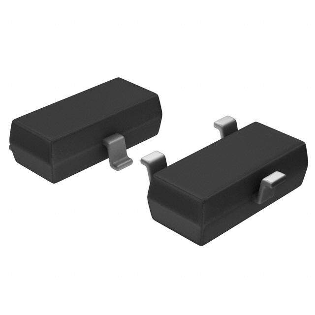
| 产品图片 |
|
| 产品型号 | RCLAMP3304N.TCT |
| rohs | 无铅 / 符合限制有害物质指令(RoHS)规范要求 |
| 产品系列 | RailClamp® |
| 不同频率时的电容 | 3.8pF @ 1MHz |
| 产品目录页面 | |
| 供应商器件封装 | SLP2626P10(2.6x2.6) |
| 其它名称 | RCLAMP3304NTCT |
| 功率-峰值脉冲 | 450W |
| 包装 | 带卷 (TR) |
| 单向通道 | - |
| 双向通道 | 4 |
| 安装类型 | 表面贴装 |
| 封装/外壳 | 10-UFDFN 裸露焊盘 |
| 工作温度 | -55°C ~ 125°C (TJ) |
| 应用 | 通用 |
| 标准包装 | 3,000 |
| 电压-击穿(最小值) | 3.5V |
| 电压-反向关态(典型值) | 3.3V (最小值) |
| 电压-箝位(最大值)@Ipp | 18V |
| 电流-峰值脉冲(10/1000µs) | 25A (8/20µs) |
| 电源线路保护 | 是 |
| 类型 | 转向装置(轨至轨) |


- 商务部:美国ITC正式对集成电路等产品启动337调查
- 曝三星4nm工艺存在良率问题 高通将骁龙8 Gen1或转产台积电
- 太阳诱电将投资9.5亿元在常州建新厂生产MLCC 预计2023年完工
- 英特尔发布欧洲新工厂建设计划 深化IDM 2.0 战略
- 台积电先进制程称霸业界 有大客户加持明年业绩稳了
- 达到5530亿美元!SIA预计今年全球半导体销售额将创下新高
- 英特尔拟将自动驾驶子公司Mobileye上市 估值或超500亿美元
- 三星加码芯片和SET,合并消费电子和移动部门,撤换高东真等 CEO
- 三星电子宣布重大人事变动 还合并消费电子和移动部门
- 海关总署:前11个月进口集成电路产品价值2.52万亿元 增长14.8%


PDF Datasheet 数据手册内容提取
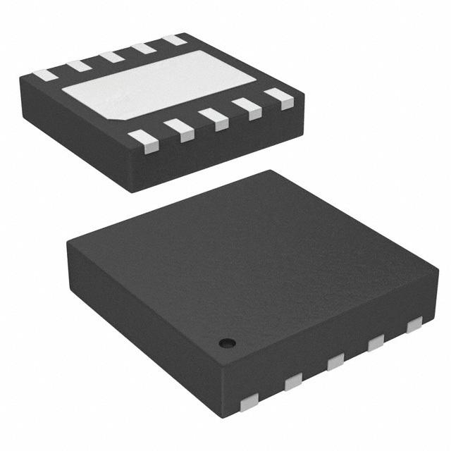
RClamp2504N & RClamp3304N RailClamp®®®®® 2.5V & 3.3V TVS Arrays ®®®®® PROTECTION PRODUCTS - RailClamp Description Features A RailClamp® is a low capacitance TVS array designed (cid:139) Transient protection for high-speed data lines to to protect high speed data interfaces. This series has IEC 61000-4-2 (ESD) 15kV (air), 8kV (contact) been specifically designed to protect sensitive compo- IEC 61000-4-4 (EFT) 40A (5/50ns) nents which are connected to data and transmission IEC 61000-4-5 (Lightning) 25A (8/20μs) lines from overvoltage caused by ESD (electrostatic (cid:139) Array of surge rated diodes with internal TVS Diode discharge), CDE (Cable Discharge Events), and Light- (cid:139) Small package saves board space ning. (cid:139) Protects up to four I/O lines The unique design incorporates surge rated, low (cid:139) Low capacitance (<5pF) for high-speed interfaces capacitance steering diodes and a TVS diode in a (cid:139) Low leakage current and clamping voltage single package. During transient conditions, the (cid:139) Low operating voltage: 2.5V and 3.3V steering diodes direct the transient current to ground. (cid:139) Solid-state silicon-avalanche technology The internal TVS diode clamps the transient voltage to a safe level. The low capacitance array configuration Mechanical Characteristics allows the user to protect up to four high-speed data (cid:139) SLP2626P10 10L package lines. (cid:139) RoHS/WEEE Compliant The RClamp®3304N and RClamp®2504N are con- (cid:139) Nominal Dimensions: 2.6 x 2.6 x 0.60 mm structed using Semtech’s proprietary EPD process technology. The EPD process provides low stand-off (cid:139) Lead Finish: NiPdAu voltages with significant reductions in leakage current (cid:139) Molding compound flammability rating: UL 94V-0 and capacitance over silicon-avalanche diode pro- (cid:139) Marking : Marking Code + Date Code cesses. They feature a true operating voltage of 2.5 (cid:139) Packaging : Tape and Reel volts and 3.3 volts for superior protection. Applications These devices are in a 10-pin, RoHS/WEEE compliant, SLP2626P10 package. It measures 2.6 x 2.6 x (cid:139) USB 2.0 0.60mm. The leads are spaced at a pitch of 0.5mm (cid:139) 10/100/1000 Ethernet and are finished with lead-free NiPdAu. The high surge (cid:139) Digital Visual Interface (DVI) capability (Ipp=25A, tp=8/20μs) means it can be used (cid:139) T1/E1 Secondary Protection in high threat environments in applications such as (cid:139) T3/E3 Secondary Protection Gigabit Ethernet, telecommunication lines, and digital (cid:139) Analog Video video. Circuit Diagram Package Configuration 2.60 CL 1 2 Pin 5 2.60 C L Pin 1 Pin 9 Pin 3 Pin 7 0.50 BSC Gnd 0.60 Revision 04/07/2009 1 www.semtech.com
RClamp2504N & RClamp3304N PROTECTION PRODUCTS Absolute Maximum Rating Rating Symbol Value Units PeakPulsePower(tp =8/20μs) P 450 Watts pk PeakPulseCurrent (tp =8/20μs) I 25 A PP ESDperIEC61000-4-2(Air) V 25 kV ESD ESDperIEC61000-4-2(Contact) 15 Operating Temperature T -55to+125 °C J StorageTemperature T -55to+150 °C STG Electrical Characteristics (T=25oC) RClamp2504N Parameter Symbol Conditions Minimum Typical Maximum Units ReverseStand-Off Voltage V 2.5 V RWM Punch-Through Voltage V I =2μA 2.7 V PT PT Snap-Back Voltage V I =50mA 2.0 V SB SB ReverseLeakageCurrent I V =2.5V, T=25°C 0.5 μA R RWM Clamping Voltage V I =1A, t =8/20μs 4.5 V C PP p Clamping Voltage V I =10A, t =8/20μs 7.5 V C PP p Clamping Voltage V I =25A, t =8/20μs 15 V C PP p Junction Capacitance C Between I/Opinsand Ground 3.8 5 pF j V =0V, f =1MHz R Between I/Opins 2.0 pF V =0V, f =1MHz R Note 1: I/O pins are pin 1, 3, 7, and 9 © 2009 Semtech Corp. 2 www.semtech.com
RClamp2504N & RClamp3304N PROTECTION PRODUCTS RClamp3304N Parameter Symbol Conditions Minimum Typical Maximum Units ReverseStand-Off Voltage V 3.3 V RWM Punch-Through Voltage V I =5μA 3.5 V PT PT Snap-Back Voltage V I =50mA 2.8 V SB SB ReverseLeakageCurrent I V =3.3V, T=25°C 0.5 μA R RWM Clamping Voltage V I =1A, t =8/20μs 5.5 V C PP p Clamping Voltage V I =10A, t =8/20μs 10.5 V C PP p Clamping Voltage V I =25A, t =8/20μs 18 V C PP p Junction Capacitance C Between I/Opinsand Ground 3.8 5 pF j V =0V, f =1MHz R Between I/Opins 2.0 pF V =0V, f =1MHz R © 2009 Semtech Corp. 3 www.semtech.com
RClamp2504N & RClamp3304N PROTECTION PRODUCTS Typical Characteristics Non-Repetitive Peak Pulse Power vs. Pulse Time Power Derating Curve 10 110 100 W) 90 er - P (kPP 1 ower or IPP 678000 w P Po ed 50 e at s R 40 k Pul 0.1 % of 30 a e 20 P 10 0 0.01 0 25 50 75 100 125 150 0.1 1 10 100 1000 Pulse Duration - tp (us) Ambient Temperature - TA (oC) Pulse Waveform Normalized Junction Capacitance vs. Reverse Voltage 110 1.5 Waveform 100 1.4 Parameters: 90 tr = 8µs 1.3 1.2 80 td = 20µs 1.1 Percent of IPP 3456700000 e-t td = IPP/2 C(V) / C(V=0)JRJR00000.....156789 0.4 20 0.3 10 0.2 0.1 f = 1 MHz 0 0 0 5 10 15 20 25 30 0 0.5 1 1.5 2 2.5 Time (µs) Reverse Voltage - VR (V) Clamping Voltage vs. Peak Pulse Current Clamping Voltage vs. Peak Pulse Current I/O to GND I/O to I/O 20 25 (V)C15 RClamp3304N (V)C20 RClamp3304N V V e - e - 15 g g a a olt 10 olt V V g g 10 RClamp2504N n n pi pi am 5 RClamp2504N Waveform am Waveform Cl Parameters: Cl 5 Parameters: tr = 8μs tr = 8μs td = 20μs td = 20μs 0 0 0 5 10 15 20 25 0 5 10 15 20 25 Peak Pulse Current - I (A) Peak Pulse Current - I (A) PP PP © 2009 Semtech Corp. 4 www.semtech.com
RClamp2504N & RClamp3304N PROTECTION PRODUCTS Typical Characteristics Insertion Loss S21 (I/O to Ground) ESD Clamping (8kV Contact per IEC 61000-4-2) CH1 S21 LOG 6 dB / REF 0 dB 1: -1.0230 dB 800 MHz 2: -1.1051 dB 0 dB 900 MHz -6 dB 1 2 3 4 3: -2.0922 dB 1.8 GHz -12 dB 4: -3.0779 dB 2.5 GHz -18 dB 5: -4.5358 dB -24 dB 2.7 GHz -30 dB -36 dB -42 dB -48 dB 1 10 100 1 3 MHz MHz MHz GHz GHz START . MHz STOP 3 000. 0000 00 MHz Note: Data is taken with a 10x attenuator © 2009 Semtech Corp. 5 www.semtech.com
RClamp2504N & RClamp3304N PROTECTION PRODUCTS Applications Information Circuit Diagram Device Connection Options for Protection of Four High-Speed Data Lines Pin 5 These devices are designed to protect low voltage data lines operating at 2.5 volts or 3.3 volts. When the voltage on the protected line exceeds the reference voltage the steering diodes are forward biased, Pin 1 Pin 9 Pin 3 Pin 7 conducting the transient current away from the sensitive circuitry. Data lines are connected at pins 1, 3, 7 and 9. The center pin should be connected directly to a ground Gnd plane. The path length is kept as short as possible to minimize parasitic inductance. Pins 2, 4, 6, 8, and 10 are not connected. Note that pin 5 is connected internally to the cathode FFFFFiiiiiggggguuuuurrrrreeeee 11111..... PPPPPiiiiinnnnn CCCCCooooonnnnnfffffiiiiiggggguuuuurrrrraaaaatttttiiiiiooooonnnnn (((((TTTTToooooppppp SSSSSiiiiidddddeeeee VVVVViiiiieeeeewwwww))))) of the low voltage TVS. It is not recommended that these pins be directly connected to a DC source greater than the snap-back voltage (V ) as the device SB can latch on as described below. 1 10 2 9 EPD TVS Characteristics 3 GND 8 These devices are constructed using Semtech’s 4 7 proprietary EPD technology. By utilizing the EPD tech- nology, the RClamp2504N and RClamp3304N can 5 6 effectively operate at 2.5V and 3.3V respectively while maintaining excellent electrical characteristics. Pin Identification The EPD TVS employs a complex nppn structure in contrast to the pn structure normally found in tradi- 1,3,7,9 Input/Output Lines tional silicon-avalanche TVS diodes. Since the EPD TVS devices use a 4-layer structure, they exhibit a 2,4,6,8,10 NoConnect slightly different IV characteristic curve when compared to conventional devices. During normal operation, the NoConnect 5 (Donot connect thispin toaDCsupply) device represents a high-impedance to the circuit up to the device working voltage (V ). During an ESD RWM CenterTab Ground event, the device will begin to conduct and will enter a low impedance state when the punch through voltage (V ) is exceeded. Unlike a conventional device, the low PT voltage TVS will exhibit a slight negative resistance characteristic as it conducts current. This characteris- defined on the curve by the snap-back voltage (V ) SB tic aids in lowering the clamping voltage of the device, and snap-back current (I ). To return to a non- SB but must be considered in applications where DC conducting state, the current through the device must voltages are present. fall below the I (approximately <50mA) and the SB voltage must fall below the V (normally 2.8 volts for a SB When the TVS is conducting current, it will exhibit a 3.3V device). If a 3.3V TVS is connected to 3.3V DC slight “snap-back” or negative resistance source, it will never fall below the snap-back voltage of characteristics due to its structure. This point is 2.8V and will therefore stay in a conducting state. © 2009 Semtech Corp. 6 www.semtech.com
RClamp2504N & RClamp3304N PROTECTION PRODUCTS Applications Information RRRCCClllaaammmppp222555000444NNN 111 222 RRRCCClllaaammmppp222555000444NNN Gigabit Ethernet 111 222 Transceiver RRRCCClllaaammmppp222555000444NNN 111 222 RRRCCClllaaammmppp222555000444NNN 111 222 Schematic Diagram for Gigabit Ethernet Telcordia GR-1089 Intra-Building Protection (PHY Operating Temp <= 90°C) 1 10 2 9 3 8 4 7 5 6 RClamp2504N 1 10 2 9 3 8 4 7 5 6 RClamp2504N Schematic Diagram for Gigabit Ethernet ESD Protection © 2009 Semtech Corp. 7 www.semtech.com
RClamp2504N & RClamp3304N PROTECTION PRODUCTS Applications Information - Spice Model RClamp2504N Spice Model RClamp2504NSpice Parameters Parameter Unit D1(LCRD) D2(LCRD) D3(TVS) IS Amp 1E-20 1E-20 1.66E-13 BV Volt 100 100 2.89 VJ Volt 0.63 0.59 0.53 RS Ohm 0.138 0.241 0.06 IBV Amp 1E-3 1E-3 1E-3 CJO Farad 1.5E-12 1.5E-12 288E-12 TT sec 2.541E-9 2.541E-9 2.541E-9 M -- 0.01 0.01 0.17 N -- 1.1 1.1 1.1 EG eV 1.11 1.11 1.11 © 2009 Semtech Corp. 8 www.semtech.com
RClamp2504N & RClamp3304N PROTECTION PRODUCTS Applications Information - Spice Model RClamp3304N Spice Model RClamp3304NSpice Parameters Parameter Unit D1(LCRD) D2(LCRD) D3(TVS) IS Amp 1E-20 1E-20 1.66E-13 BV Volt 100 100 3.55 VJ Volt 0.62 0.59 0.6 RS Ohm 0.138 0.241 0.182 IBV Amp 1E-3 1E-3 1E-3 CJO Farad 1.5E-12 1.5E-12 253E-12 TT sec 2.541E-9 2.541E-9 2.541E-9 M -- 0.01 0.01 0.205 N -- 1.1 1.1 1.1 EG eV 1.11 1.11 1.11 © 2009 Semtech Corp. 9 www.semtech.com
RClamp2504N & RClamp3304N PROTECTION PRODUCTS Outline Drawing - SLP2626P10 A D B DIMENSIONS INCHES MILLIMETERS DIM MINNOMMAX MINNOMMAX A .020 .024 .026 0.50 0.60 0.65 PIN 1 A1 .000 .001 .002 0.00 0.03 0.05 (LASINEDRIC MAATROKR) E Ab2 .007(..000170).012 0.20(00..2157)0.30 D .098 .102 .106 2.50 2.60 2.70 D1 .079 .085 .089 2.00 2.15 2.25 E .098 .102 .106 2.50 2.60 2.70 E1 .044 .050 .054 1.11 1.26 1.36 e .020 BSC 0.50 BSC L .011 .014 .016 0.30 0.35 0.40 A SEATING N 10 10 aaa C PLANE aaa .003 0.08 bbb .004 0.10 A2 D1 A1 C 1 2 CL E/2 CL E1 LxN N e bxN D/2 bbb C A B NOTES: 1. CONTROLLING DIMENSIONS ARE IN MILLIMETERS (ANGLES IN DEGREES). 2. COPLANARITY APPLIES TO THE EXPOSED PAD AS WELL AS THE TERMINALS. Land Pattern - SLP2626P10 P X DIMENSIONS DIM INCHES MILLIMETERS B .081 2.05 C .100 2.50 Z F (C) F .050 1.26 G G .073 1.85 P .020 0.50 X .012 0.30 Y .025 0.65 Z .124 3.15 Y B NOTES: 1. THIS LAND PATTERN IS FOR REFERENCE PURPOSES ONLY. CONSULT YOUR MANUFACTURING GROUP TO ENSURE YOUR COMPANY'S MANUFACTURING GUIDELINES ARE MET. © 2009 Semtech Corp. 10 www.semtech.com
RClamp2504N & RClamp3304N PROTECTION PRODUCTS Marking Ordering Information Working Qtyper 2504N 3304N Part Number ReelSize Voltage Reel YYWW YYWW RClamp2504N.TCT 2.5Volts 3,000 7Inch RClamp3304N.TCT 3.3Volts 3,000 7Inch RClamp2504N RClamp3304N RailClamp and RClamp are marks of Semtech Corporation YYWW = Date Code Tape and Reel Specification Pin 1 Location User Direction of feed Device Orientation in Tape A0 B0 K0 2.77+/-0.10mm 2.77+/-0.10mm 0.80+/-0.10mm Tape K B,(Max) D D1 E F P P0 P2 T(MAX) W Width (MAX) 8.0mm 1.0mm 1.750±.10 4.2mm 1.5+0.1mm 3.5±0.05 4.0±0.1 4.0±0.1 2.0±0.05 +0.3mm 8mm ±0.05 mm 2.4mm 0.4mm (.165) -0.0mm mm mm mm mm -0.1mm Contact Information Semtech Corporation Protection Products Division 200 Flynn Rd., Camarillo, CA 93012 Phone: (805)498-2111 FAX (805)498-3804 © 2009 Semtech Corp. 11 www.semtech.com