ICGOO在线商城 > 集成电路(IC) > 嵌入式 - PLD(可编程逻辑器件) > ATF16V8C-7SU

 Datasheet下载
- 型号: ATF16V8C-7SU
- 制造商: Atmel
- 库位|库存: xxxx|xxxx
- 要求:
| 数量阶梯 | 香港交货 | 国内含税 |
| +xxxx | $xxxx | ¥xxxx |
查看当月历史价格
查看今年历史价格
ATF16V8C-7SU产品简介:
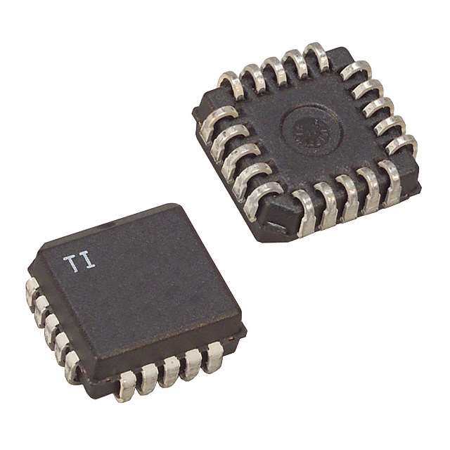
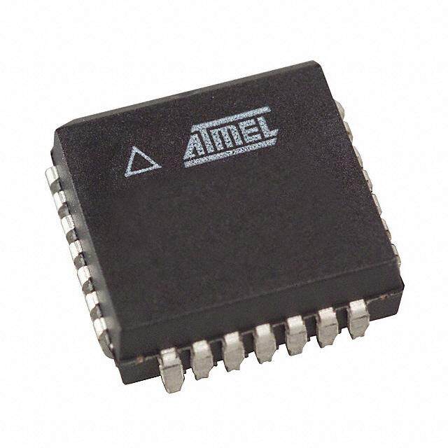
ICGOO电子元器件商城为您提供ATF16V8C-7SU由Atmel设计生产,在icgoo商城现货销售,并且可以通过原厂、代理商等渠道进行代购。 ATF16V8C-7SU价格参考。AtmelATF16V8C-7SU封装/规格:嵌入式 - PLD(可编程逻辑器件), 16V8 Programmable Logic Device (PLD) IC 8 Macrocells 7.5ns 20-SOIC。您可以下载ATF16V8C-7SU参考资料、Datasheet数据手册功能说明书,资料中有ATF16V8C-7SU 详细功能的应用电路图电压和使用方法及教程。
Microchip Technology的ATF16V8C-7SU是一种高性能的可编程逻辑器件(PLD),广泛应用于需要定制化逻辑功能和接口转换的场景。该器件属于20引脚封装的CMOS型可编程逻辑阵列,具有低功耗、高可靠性和可重复编程等优点,适用于中小规模逻辑控制。

其典型应用场景包括:

1. 接口逻辑控制:用于实现不同芯片或模块之间的信号转换与协调,如将不同电平标准或时序要求的信号进行适配,广泛应用于通信接口、数据总线控制等领域。

2. 状态机设计:适合实现各种组合逻辑与时序逻辑控制,例如工业自动化控制系统中的状态转换逻辑、设备控制逻辑等。

3. 地址解码与片选控制:在嵌入式系统或微控制器系统中,用于对外设芯片进行地址译码和片选信号生成,提高系统集成度和灵活性。

4. 替代传统逻辑电路:可替代多个74系列逻辑芯片,减少PCB面积,简化设计并提高系统可靠性。

5. 原型验证与快速开发:在产品开发初期用于验证逻辑设计,便于修改和优化逻辑功能,缩短开发周期。

ATF16V8C-7SU适用于工业控制、通信设备、消费电子、汽车电子等领域,是实现定制化逻辑控制的理想选择。
| 参数 | 数值 |
| 产品目录 | 集成电路 (IC) |
| 描述 | IC PLD 8MC 7.5NS 20SOIC |
| 产品分类 | |
| 品牌 | Atmel |
| 数据手册 | |
| 产品图片 |
|
| 产品型号 | ATF16V8C-7SU |
| rohs | 无铅 / 符合限制有害物质指令(RoHS)规范要求 |
| 产品系列 | 16V8 |
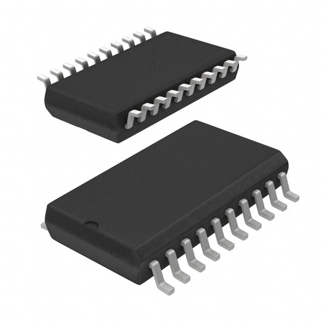
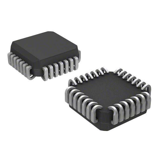
| 供应商器件封装 | 20-SOIC W |
| 其它名称 | ATF16V8C7SU |
| 包装 | 管件 |
| 可编程类型 | EE PLD |
| 安装类型 | 表面贴装 |
| 宏单元数 | 8 |
| 封装/外壳 | 20-SOIC(0.295",7.50mm 宽) |
| 标准包装 | 37 |
| 电压-输入 | 5V |
| 速度 | 7.5ns |


- 商务部:美国ITC正式对集成电路等产品启动337调查
- 曝三星4nm工艺存在良率问题 高通将骁龙8 Gen1或转产台积电
- 太阳诱电将投资9.5亿元在常州建新厂生产MLCC 预计2023年完工
- 英特尔发布欧洲新工厂建设计划 深化IDM 2.0 战略
- 台积电先进制程称霸业界 有大客户加持明年业绩稳了
- 达到5530亿美元!SIA预计今年全球半导体销售额将创下新高
- 英特尔拟将自动驾驶子公司Mobileye上市 估值或超500亿美元
- 三星加码芯片和SET,合并消费电子和移动部门,撤换高东真等 CEO
- 三星电子宣布重大人事变动 还合并消费电子和移动部门
- 海关总署:前11个月进口集成电路产品价值2.52万亿元 增长14.8%

PDF Datasheet 数据手册内容提取
Features • Industry-standard architecture – Emulates Many 20-pin PALs® – Low-cost, easy to use software tools • High speed electrically-erasable programmable logic devices (EE PLD) – 5ns maximum pin-to-pin delay • Low power, 100μA pin controlled power-down mode option • CMOS and TTL compatible inputs and outputs – I/O pin keeper circuits High Performance • Advanced flash technology Electrically-erasable – Reprogrammable Programmable – 100% tested • High reliability CMOS process Logic Devices – 20 year data retention – 100 erase/write cycles – 2,000V ESD protection Atmel ATF16V8C – 200mA latchup immunity • Commercial and industrial temperature ranges • Dual-in-line and surface mount packages in standard pinouts • PCI compliant • Green (ROHS compliant) package options available Description The Atmel® ATF16V8C is a high performance EECMOS programmable logic device (PLD) that utilizes the Atmel proven electrically-erasable (EE) Flash memory technology. Offered options include speeds down to 5ns and a 100μA pin-controlled power-down mode. All speed ranges are specified over the full 5V ± 10% range for industrial temperature ranges, and 5V ± 5% for commercial range 5V devices. The ATF16V8C incorporates a superset of the generic architectures, which allows direct replacement of the 16R8 family and most 20-pin combinatorial PLDs. Eight outputs are each allocated eight product terms. Three different modes of operation are configured auto- matically with software, and allow highly complex logic functions to be realized. The ATF16V8C can significantly reduce total system power, thereby enhancing system reli- ability and reducing power supply costs. When pin 4 is configured as the power-down control pin, supply current drops to less than 100μA whenever the pin is high. If the power- down feature isn't required for a particular application, pin 4 may be used as a logic input. Also, the pin-keeper circuits eliminate the need for internal pull-up resistors along with their attendant power consumption. 0425H–PLD–3/11
Figure 0-1. Block diagram Note: 1. Includes optional PD control pin Figure 0-2. Pin configurations Pin name Function CLK Clock I Logic inputs I/O Bidirectinoal buffers OE Output enable V +5V supply CC PD Power-down TSSOP DIP/SOIC PLCC Top view Top view Top view K I/CLK 1 20 VCC L C I1 2 19 I/O I/CLK 1 20 VCC I2 I1 I/C VC I/O I1 2 19 I/O I2 3 18 I/O 3 2 1 0 9 I2 3 18 I/O 2 1 PD/I3 4 17 I/O PD/I3 4 18 I/O PD/I3 4 17 I/O I4 5 16 I/O I4 5 17 I/O I4 5 16 I/O I5 6 15 I/O I5 6 16 I/O I5 6 15 I/O I6 7 14 I/O I6 7 15 I/O I6 7 14 I/O I7 8 13 I/O I7 8 14 I/O I7 8 13 I/O 0 1 2 3 I8 9 12 I/O 9 1 1 1 1 I8 9 12 I/O GND 10 11 I9/OE 8 D E O O GND 10 11 I9/OE I N O I/ I/ G 9/ I Atmel ATF16V8C 2 0425H–PLD–3/11
Atmel ATF16V8C 1. Absolute maximum ratings* Temperature under bias. . . . . . . . . . . . . . . . . . . . . . . .-40C to +85C *NOTICE: Stresses beyond those listed under “Absolute maximum ratings” may cause permanent damage to the device. This is a stress rating only, and functional Storage temperature. . . . . . . . . . . . . . . . . . . . . . . . . .-65C to +150C operation of the device at these or any other conditions beyond those indicated in the operational sections of Voltage on any pin with respect to ground. . . . . -2.0V to +7.0V(1) this specification is not implied. Exposure to absolute maximum rating conditions for extended periods may Voltage on input pins with respect to ground affect device reliability. during programming . . . . . . . . . . . . . . . . . . . . . . . .-2.0V to +14.0V(1) Note: 1. Minimum voltage is -0.6V DC, which may undershoot to -2.0V for pulses of less than 20ns. Maximum out- Programming voltage with put pin voltage is V + 0.75V DC, which may CC respect to ground. . . . . . . . . . . . . . . . . . . . . . . . . . .-2.0V to +14.0V(1) overshoot to 7.0V for pulses of less than 20ns. 2. DC and AC characteristics Table 2-1. DC and AC operating conditions Commercial Industrial Operating temperature (Ambient) 0C - 70C -40C - 85C V power supply 5V ± 5% 5V ± 10% CC Table 2-2. DC characteristics Symbol Parameter Condition Min Typ Max Units I Input or I/O low leakage current 0 V V (Max) -10.0 μA IL IN IL I Input or I/O high leakage current 3.5 V V 10.0 μA IH IN CC 15MHz, V = Max, Com. 115 mA I (1) Power supply current, standby CC CC1 V = 0, V , outputs open IN CC Ind. 130 mA Power supply current, Com. 10 100 μA I V = Max, V = 0, V PD Power-down mode CC IN CC Ind. 10 105 μA V = 0.5V; I Output short circuit current OUT -150 mA OS V = 5V; T = 25°C CC A V Input low voltage Min < V < Max -0.5 0.8 V IL CC V Input high voltage 2.0 V + 1 V IH CC V = Min; All outputs V Output low voltage CC Com., Ind. 0.5 V OL I = 24mA OL V = Min V Output high voltage CC 2.4 V OH I = -4.0mA OL Com. 24.0 mA I Output low current V = Min OL CC Ind. 12.0 mA I Output high current V = Min Com., Ind. -4.0 mA OH CC Note: 1. All I parameters measured with outputs open CC 3 0425H–PLD–3/11
Figure 3. AC waveforms Note: 1. Timing measurement reference is 1.5V. Input AC driving levels are 0.0V and 3.0V, unless otherwise specified. Table 3-1. AC characteristics -5 -7 -10 Symbol Parameter Min Max Min Max Min Max Units t Input or feedback to non-registered output 1 5 3 7.5 3 10 ns PD t Clock to feedback 3 3 6 ns CF t Clock to output 1 4 2 5 2 7 ns CO t Input or feedback setup time 3 5 7.5 ns S t Input hold time 0 0 0 ns H t Clock period 6 8 12 ns P t Clock width 3 4 6 ns W External feedback 1/(t + t ) 142 100 68 MHz S CO f Internal feedback 1/(t + t ) 166 125 74 MHz MAX S CF No feedback 1/(t ) 166 125 83 MHz P t Input to output enable – product term 2 6 3 9 3 10 ns EA t Input to output disable – product term 2 5 2 9 2 10 ns ER t OE pin to output enable 2 5 2 6 2 10 ns PZX t OE pin to output disable 1.5 5 1.5 6 1.5 10 ns PXZ Atmel ATF16V8C 4 0425H–PLD–3/11
Atmel ATF16V8C Table 3-2. Power-down AC characteristics(1)(2)(3) -5 -7 -10 Symbol Parameter Min Max Min Max Min Max Units t Valid Input before PD High 5.0 7.5 10 ns IVDH t Valid OE before PD High 0 0 0 ns GVDH t Valid Clock before PD High 0 0 0 ns CVDH t Input Don’t Care after PD High 5.0 7.5 10 ns DHIX t OE Don’t Care after PD High 5.0 7.5 10 ns DHGX t Clock Don’t Care after PD High 5.0 7.5 10 ns DHCX t PD Low to Valid Input 5.0 7.5 10 ns DLIV t PD Low to Valid OE 15.0 20.0 25 ns DLGV t PD Low to Valid Clock 15.0 20.0 25 ns DLCV t PD Low to Valid Output 20.0 25.0 30 ns DLOV Note: 1. Output data is latched and held 2. HI-Z outputs remain HI-Z 3. Clock and input transitions are ignored 4. Input test waveforms and measurement levels: t , t < 1.5ns (10% to 90%) R F 5. Output test loads 5.0V R1 = 200 OUTPUT PIN R2 = 200 CL = 50 pF 6. Pin capacitance Table 6-1. Pin capacitance Typ Max Units Conditions C 5 8 pF V = 0V IN IN C 6 8 pF V = 0V OUT OUT Note: 1. Typical values for nominal supply voltage. This parameter is only sampled and is not 100% tested. 5 0425H–PLD–3/11
7. Power-up reset Registers of the ATF16V8C are designed to reset during power-up. At a point delayed slightly from V crossing V , all CC RST registers will be reset to the low state. As a result, the registered output state will always be high on power-up. This feature is critical for state machine initialization. However,due to the asynchronous nature of reset and the uncertainty of how V actually rises in the system, the followingconditions are required: CC 1. The V rise must be monotonic, from below 0.7V CC 2. After reset occurs, all input and feedback setup times must be met before driving the clock term high, and 3. The signals from which the clock is derived must remain stable during t PR Figure 8. Power-up reset Table 8-1. Power-up reset parameters Parameter Description Typ Max Units t Power-up PR 600 1,000 ns Reset Time V Power-up RST 3.8 4.5 V Reset Voltage 9. Power-down mode The ATF16V8C includes an optional pin controlled powerdown feature. Device pin 4 may be configured as the power- down pin. When this feature is enabled and the power-down pin is high, total current consumption drops to less than 100μA. In the power-down mode, all output data and internal logic states are latched and held. All registered and combinatorial output data remains valid. Any outputs that were in a high-Z state at the onset of power-down will remain at high-Z. During power-down, all input signals except the power-down pin are blocked. The input and I/O pin-keeper circuits remain active to insure that pins do not float to indeterminate levels. This helps to further reduce system power. Selection of the power-down option is specified in the ATF16V8C logic design file. The logic compiler will include this option selection in the otherwise standard 16V8 JEDEC fuse file. When the power-down feature is not specified in the design file, pin 4 is available as a logic input, and there is no power-down pin. This allows the ATF16V8C to be programmed using any existing standard 16V8 fuse file. Note: Some programmers list the JEDEC-compatible 16V8C (No PD used) separately from the non-JEDEC compatible 16V8CEXT. (EXT for extended features.) 10. Registered output preload Registers of the ATF16V8C are provided with circuitry to allow loading of each register with either a high or a low. This feature will simplify testing since any state can be forced into the registers to control test sequencing. A JEDEC file with preload is generated when a source file with vectors is compiled. Once downloaded, the JEDEC file preload sequence will be done automatically by approved programmers. Atmel ATF16V8C 6 0425H–PLD–3/11
Atmel ATF16V8C 11. Security fuse usage A single fuse is provided to prevent unauthorized copying of the ATF16V8C fuse patterns. Once programmed, fuse verify and preload are inhibited. However, the 64-bit user signature remains accessible. The security fuse will be programmed last, as its effect is immediate. 12. Input and I/O pin-keeper circuits The ATF16V8C contains internal input and I/O pin-keeper circuits. These circuits allow each ATF16V8C pin to hold its previous value even when it is not being driven by an externalsource or by the device’s output buffer. This helps insure that all logic array inputs are at known, valid logic levels. This reduces system power by preventing pins from floating to indeterminate levels. By using pin-keeper circuits rather than pull-up resistors, there is no DC current required to hold the pins in either logic state (high or low). These pin-keeper circuits are implemented as weak feedback inverters, as shown in the Input Diagram below. These keeper circuits can easily be overdriven by standard TTL- or CMOS-compatible drivers. The typical overdrive current required is 40μA. Figure 13. Input diagram Figure 14. I/O diagram 7 0425H–PLD–3/11
15. Functional logic diagram description The logic option and functional diagrams describe the ATF16V8C architecture. Eight configurable macrocells can be configured as a registered output, combinatorial I/O, combinatorial output, or dedicated input. The ATF16V8C can be configured in one of three different modes. Each mode makes the ATF16V8C look like a different device. Most PLD compilers can choose the right mode automatically. The user can also force the selection by supplying the compiler with a mode selection. The determining factors would be the usage of register versus combinatorial outputs and dedicated outputs versus outputs with output enable control. The ATF16V8C universal architecture can be programmed to emulate many 20-pin PAL devices. These architectural subsets can be found in each of the configuration modes described in the following pages. The user can download the listed subset device JEDEC programming file to the PLD programmer, and the ATF16V8C can be configured to act like the chosen device. Check with your programmer manufacturer for this capability. Unused product terms are automatically disabled by the compiler to decrease power consumption. A security fuse, when programmed, protects the content of the ATF16V8C. Eight bytes (64 fuses) of user signature are accessible to the user for purposes such as storing project name, part number, revision, or date. The user signature is accessible regardless of the state of the security fuse. Table 15-1. Compiler mode selection Registered Complex Simple Auto select ABEL, Atmel-ABEL P16V8R P16V8C P16V8AS P16V8 With PD ENABLE P16V8PDR(1) P16V8PDC(1) P16V8PD(1) P16V8PDS(1) CUPL, Atmel-CUPL G16V8MS G16V8MA G16V8AS G16V8A With PD ENABLE G16V8CPMS G16V8CPMA G16V8CPAS G16V8CP LOG/iC GAL16V8_R(2) GAL16V8_C7(2) GAL16V8_C8(2) GAL16V8 OrCAD-PLD “Registered” “Complex” “Simple” GAL16V8A PLDesigner P16V8R P16V8C P16V8C P16V8A Synario/Atmel-Synario NA NA NA ATF16V8C ALL With PD ENABLE NA NA NA ATF16V8C (PD) ALL(1) Tango-PLD G16V8R G16V8C G16V8AS G16V8 Note: 1. Please call Atmel PLD Hotline at (408) 436-4333 for more information 2. Only applicable for version 3.4 or lower 16. Macrocell configuration Software compilers support the three different OMC modes as different device types. These device types are listed in the table below. Most compilers have the ability to automatically select the device type, generally based on the register usage and output enable (OE) usage. Register usage on the device forces the software to choose the registered mode. All combinatorial outputs with OE controlled by the product term will force the software to choose the complex mode. The software will choose the simple mode only when all outputs are dedicated combinatorial without OE control. The different device types listed in the table can be used to override the automatic device selection by the software. For further details, refer to the compiler software manuals. When using compiler software to configure the device, the user must pay special attention to the following restrictions in each mode. In registered mode, pin 1 and pin 11 are permanently configured as clock and output enable, respectively. These pins cannot be configured as dedicated inputs in the registered mode. In complex mode, pin 1 and pin 11 become dedicated inputs and use the feedback paths of pin 19 and pin 12 respectively. Because of this feedback path usage, pin 19 and pin 12 do not have the feedback option in this mode. Atmel ATF16V8C 8 0425H–PLD–3/11
Atmel ATF16V8C In simple mode, all feedback paths of the output pins are routed via the adjacent pins. In doing so, the two inner most pins (pins 15 and 16) will not have the feedback option as these pins are always configured as dedicated combinatorial output. 16.1 Atmel ATF16V8C registered mode PAL device emulation/PAL replacement. The registered mode is used if one or more registers are required. Each macrocell can be configured as either a registered or combinatorial output or I/O, or as an input. For a registered output or I/O, the output is enabled by the OE pin, and the register is clocked by the CLK pin. Eight productterms are allocated to the sum term. For a combinatorial output or I/O, the output enable is controlled by a product term, and seven product terms are allocated to the sum term. When the macrocell is configured as an input, the output enable is permanently disabled. Any register usage will make the compiler select this mode. The following registered devices can be emulated using this mode: 16R8 16RP8 16R6 16RP6 16R4 16RP4 Figure 17. Registered configuration for registered mode(1)(2) Notes: 1. Pin 1 controls common CLK for the registered outputs. Pin 11 controls common OE for the registered outputs. Pin 1 and Pin 11 are permanently configured as CLKand OE. 2. The development software configures all the architecture control bits and checks for proper pin usage automatically. Figure 18. Combinatorial configuration for registered mode(1)(2) Notes: 1. Pin 1 and Pin 11 are permanently configured as CLK and OE. 2. The development software configures all the architecture control bits and checks for proper pin usage automatically. 9 0425H–PLD–3/11
Figure 19. Registered mode logic diagram Note: * Input not available if power-down mode is enabled Atmel ATF16V8C 10 0425H–PLD–3/11
Atmel ATF16V8C 20. Atmel ATF16V8C complex mode PAL device emulation/PAL replacement. In the complex mode, combinatorial output and I/O functions are possible. Pins 1 and 11 are regular inputs to the array. Pins 13 through 18 have pin feedback paths back to the AND-array, which makes full I/O capability possible. Pins 12 and 19 (outermost macrocells) are outputs only. They do not have input capability. In this mode, each macrocellhas seven product terms going to the sum term and one product term enabling the output. Combinatorial applications with an OE requirement will make the compiler select this mode. The following devices can be emulated using this mode: 16L8 16H8 16P8 Figure 21. Complex Mode Option 22. Atmel ATF16V8C simple mode PAL device emulation/PAL replacement. In the simple mode, eight product terms are allocated to the sum term. Pins 15 and 16 (center macrocells) are permanently configured as combinatorial outputs. Other macrocells can be either inputs or combinatorial outputs with pin feedback to the AND-array. Pins 1 and 11 are regular inputs. The compiler selects this mode when all outputs are combinatorial without OE control. The following simple PALs can be emulated using this mode: 10L8 10H8 10P8 12L6 12H6 12P6 14L4 14H4 14P4 16L2 16H2 16P2 Figure 23. Simple mode option 0 1 11 0425H–PLD–3/11
Figure 24. Complex mode logic diagram Note: * Input not available if power-down mode is enabled Atmel ATF16V8C 12 0425H–PLD–3/11
Atmel ATF16V8C Note: Simple mode logic diagram Note: * Input not available if power-down mode is enabled 13 0425H–PLD–3/11
Atmel ATF16V8C 14 0425H–PLD–3/11
Atmel ATF16V8C 15 0425H–PLD–3/11
Atmel ATF16V8C 16 0425H–PLD–3/11
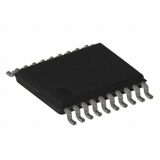
Atmel ATF16V8C 25. Ordering information t (ns) t (ns) t (ns) Atmel ordering code* Package Operation range PD S CO Commercial 5 3 4 ATF16V8C-5JX 20J (0C to 70C) ATF16V8C-7JU 20J Industrial 7.5 5 5 ATF16V8C-7PU 20P3 (-40C to 85C) ATF16V8C-7SU 20S Commercial 5 3 4 ATF16V8C-5JC 20J (0C to 70C) ATF16V8C-7JC 20J ATF16V8C-7PC 20P3 Commercial ATF16V8C-7SC 20S (0C to 70C) ATF16V8C-7XC 20X 7.5 5 5 ATF16V8C-7JI 20J ATF16V8C-7PI 20P3 Industrial ATF16V8C-7SI 20S (-40C to 85C) ATF16V8C-7XI 20X Industrial 10 7.5 7 ATF16V8C-10JI 20J (-40C to 85C) Using “C” Product for Industrial To use commercial product for Industrial temperature ranges, down-grade one speed grade from the “I” to the “C” device (7ns “C” = 10ns “I”) and de-rate power by 30%. Notes: 1. *Shaded parts are being obsoleted in 2011 2. The suffix, “U” and “X” as part of the ordering code, implies the package is ROHS compliant and lead free Package type 20J 20-lead, Plastic J-leaded Chip Carrier (PLCC) 20P3 20-lead, 0.300" Wide, Plastic Dual Inline Package (PDIP) 20S 20-lead, 0.300" Wide, Plastic Gull-Wing Small Outline (SOIC) 20X 20-lead, 4.4 mm Wide, Plastic Thin Shrink Small Outline (TSSOP) 17 0425H–PLD–3/11
26. Package Drawings 20J – PLCC 1.14(0.045) X 45˚ PIN NO. 1 1.14(0.045) X 45˚ 0.318(0.0125) IDENTIFIER 0.191(0.0075) e E1 E D2/E2 B1 B A2 D1 A1 D A 0.51(0.020)MAX 45˚ MAX (3X) COMMON DIMENSIONS (Unit of Measure = mm) SYMBOL MIN NOM MAX NOTE A 4.191 – 4.572 A1 2.286 – 3.048 A2 0.508 – – D 9.779 – 10.033 D1 8.890 – 9.042 Note 2 E 9.779 – 10.033 Notes: 1.This package conforms to JEDEC reference MS-018, Variation AA. 2.Dimensions D1 and E1 do not include mold protrusion. E1 8.890 – 9.042 Note 2 Allowable protrusion is .010"(0.254 mm) per side. Dimension D1 D2/E2 7.366 – 8.382 and E1 include mold mismatch and are measured at the extreme B 0.660 – 0.813 material condition at the upper or lower parting line. 3. Lead coplanarity is 0.004" (0.102 mm) maximum. B1 0.330 – 0.533 e 1.270 TYP 10/04/01 TITLE DRAWING NO. REV. 2325 Orchard Parkway 20J, 20-lead, Plastic J-leaded Chip Carrier (PLCC) San Jose, CA 95131 20J B R Atmel ATF16V8C 18 0425H–PLD–3/11
Atmel ATF16V8C 20P3 – PDIP D PIN 1 E1 A SEATING PLANE A1 L B B1 e E COMMON DIMENSIONS (Unit of Measure = mm) C SYMBOL MIN NOM MAX NOTE eC eB A – – 5.334 A1 0.381 – – D 24.892 – 26.924 Note 2 E 7.620 – 8.255 E1 6.096 – 7.112 Note 2 B 0.356 – 0.559 B1 1.270 – 1.551 Notes: 1.This package conforms to JEDEC reference MS-001, Variation AD. 2.Dimensions D and E1 do not include mold Flash or Protrusion. L 2.921 – 3.810 Mold Flash or Protrusion shall not exceed 0.25 mm (0.010"). C 0.203 – 0.356 eB – – 10.922 eC 0.000 – 1.524 e 2.540 TYP 1/23/04 TITLE DRAWING NO. REV. 2325 Orchard Parkway 20P3, 20-lead (0.300"/7.62 mm Wide) Plastic Dual R San Jose, CA 95131 Inline Package (PDIP) 20P3 D 19 0425H–PLD–3/11
20S – SOIC Atmel ATF16V8C 20 0425H–PLD–3/11
Atmel ATF16V8C 20X – TSSOP Dimensions in Millimeters and (Inches). Controlling dimension: Millimeters. JEDEC Standard MO-153 AC INDEX MARK PIN 1 4.50 (0.177) 6.50 (0.256) 4.30 (0.169) 6.25 (0.246) 6.60 (.260) 1.20 (0.047) MAX 6.40 (.252) 0.65 (.0256) BSC 0.15 (0.006) SEATING 0.30 (0.012) 0.05 (0.002) PLANE 0.19 (0.007) 0.20 (0.008) 0º ~ 8º 0.09 (0.004) 0.75 (0.030) 0.45 (0.018) 10/23/03 TITLE DRAWING NO. REV. 2325 Orchard Parkway 20X, (Formerly 20T), 20-lead, 4.4 mm Body Width, San Jose, CA 95131 20X C R Plastic Thin Shrink Small Outline Package (TSSOP) 21 0425H–PLD–3/11
27. Revision history Doc. rev. Date Comments Added green (ROHS compliant) package options 0425H 03/2011 Removed lead based packaged from ordering section Atmel ATF16V8C 22 0425H–PLD–3/11
Atmel Corporation Atmel Asia Limited Atmel Munich GmbH Atmel Japan 2325 Orchard Parkway Unit 01-5 & 16, 19F Business Campus 9F, Tonetsu Shinkawa Bldg. San Jose, CA 95131 BEA Tower, Millennium City 5 Parkring 4 1-24-8 Shinkawa USA 418 Kwun Tong Road D-85748 Garching b. Munich Chuo-ku, Tokyo 104-0033 Tel: (+1) (408) 441-0311 Kwun Tong, Kowloon GERMANY JAPAN Fax: (+1) (408) 487-2600 HONG KONG Tel: (+49) 89-31970-0 Tel: (+81) (3) 3523-3551 www.atmel.com Tel: (+852) 2245-6100 Fax: (+49) 89-3194621 Fax: (+81) (3) 3523-7581 Fax: (+852) 2722-1369 © 2011 Atmel Corporation. All rights reserved. / Rev.: 0425H–PLD–3/11 Atmel®, logo and combinations thereof, and others are registered trademarks or trademarks of Atmel Corporation or its subsidiaries. Other terms and product names may be trade- marks of others. Disclaimer: The information in this document is provided in connection with Atmel products. No license, express or implied, by estoppel or otherwise, to any intellectual property right is granted by this document or in connection with the sale of Atmel products. EXCEPT AS SET FORTH IN THE ATMEL TERMS AND CONDITIONS OF SALES LOCATED ON THE ATMEL WEBSITE, ATMEL ASSUMES NO LIABILITY WHATSOEVER AND DISCLAIMS ANY EXPRESS, IMPLIED OR STATUTORY WARRANTY RELATING TO ITS PRODUCTS INCLUDING, BUT NOT LIMITED TO, THE IMPLIED WARRANTY OF MERCHANTABILITY, FITNESS FOR A PARTICULAR PURPOSE, OR NON-INFRINGEMENT. IN NO EVENT SHALL ATMEL BE LIABLE FOR ANY DIRECT, INDIRECT, CONSEQUENTIAL, PUNITIVE, SPECIAL OR INCIDENTAL DAMAGES (INCLUDING, WITHOUT LIMITATION, DAMAGES FOR LOSS AND PROFITS, BUSINESS INTERRUPTION, OR LOSS OF INFORMATION) ARISING OUT OF THE USE OR INABILITY TO USE THIS DOCUMENT, EVEN IF ATMEL HAS BEEN ADVISED OF THE POSSIBILITY OF SUCH DAMAGES. Atmel makes no representations or warranties with respect to the accuracy or completeness of the contents of this document and reserves the right to make changes to specifications and products descriptions at any time without notice. Atmel does not make any commitment to update the information contained herein. Unless specifically provided otherwise, Atmel products are not suitable for, and shall not be used in, automotive applications. Atmel products are not intended, authorized, or warranted for use as components in applications intended to support or sustain life.