ICGOO在线商城 > 集成电路(IC) > 嵌入式 - PLD(可编程逻辑器件) > ATF22V10C-5JX
 Datasheet下载
- 型号: ATF22V10C-5JX
- 制造商: Atmel
- 库位|库存: xxxx|xxxx
- 要求:
| 数量阶梯 | 香港交货 | 国内含税 |
| +xxxx | $xxxx | ¥xxxx |
查看当月历史价格
查看今年历史价格
ATF22V10C-5JX产品简介:
ICGOO电子元器件商城为您提供ATF22V10C-5JX由Atmel设计生产,在icgoo商城现货销售,并且可以通过原厂、代理商等渠道进行代购。 ATF22V10C-5JX价格参考。AtmelATF22V10C-5JX封装/规格:嵌入式 - PLD(可编程逻辑器件), 22V10 Programmable Logic Device (PLD) IC 10 Macrocells 5ns 28-PLCC (11.51x11.51)。您可以下载ATF22V10C-5JX参考资料、Datasheet数据手册功能说明书,资料中有ATF22V10C-5JX 详细功能的应用电路图电压和使用方法及教程。
Microchip Technology的ATF22V10C-5JX是一款高性能的可编程逻辑器件(PLD),属于通用型可编程逻辑器件(GAL)系列。该器件广泛应用于需要中等规模逻辑控制和接口管理的嵌入式系统中。

其主要应用场景包括:

1. 工业控制:用于自动化设备中的逻辑控制、状态机设计及信号处理,如PLC(可编程逻辑控制器)、传感器接口管理和电机控制。

2. 通信设备:在通信系统中实现协议转换、时序控制与接口逻辑,适用于数据通信设备中的地址解码与总线管理。

3. 消费电子:用于家电或智能设备中的控制逻辑,如键盘扫描、LED显示控制及电源管理模块。

4. 汽车电子:应用于车身控制模块(BCM)、仪表盘控制、灯光控制系统等对可靠性要求较高的场景。

5. 测试与测量仪器:作为逻辑分析仪、示波器等设备中的控制核心,实现高速信号采集与处理。

6. 教育与研发:因其易于编程与调试,常用于高校教学及原型设计中,帮助学生理解数字电路设计与PLD应用。

ATF22V10C-5JX具备高可靠性和灵活的编程能力,适合多种中小规模逻辑控制需求,在各类嵌入式系统中发挥着关键作用。
| 参数 | 数值 |
| 产品目录 | 集成电路 (IC) |
| 描述 | IC PLD 10MC 5NS 28PLCC |
| 产品分类 | |
| 品牌 | Atmel |
| 数据手册 | |
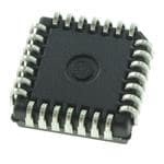
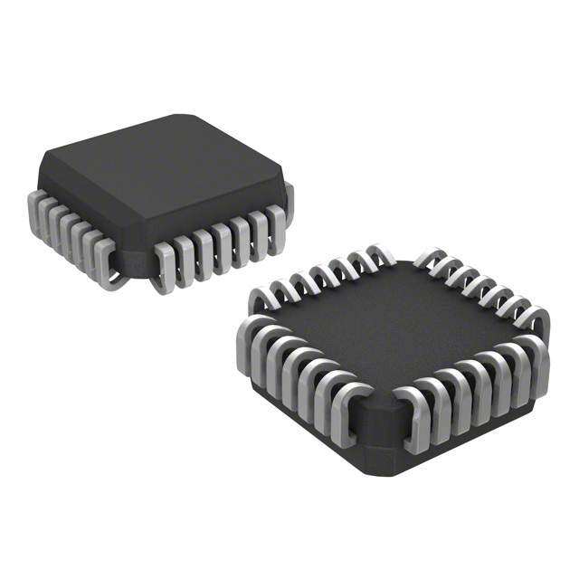
| 产品图片 |
|
| 产品型号 | ATF22V10C-5JX |
| rohs | 无铅 / 符合限制有害物质指令(RoHS)规范要求 |
| 产品系列 | 22V10 |
| 供应商器件封装 | 28-PLCC(11.51x11.51) |
| 其它名称 | ATF22V10C5JX |
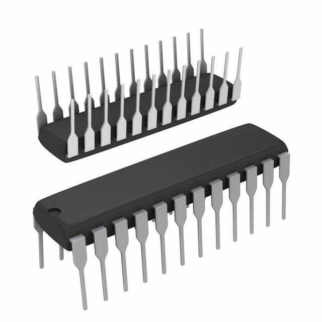
| 包装 | 管件 |
| 可编程类型 | EE PLD |
| 安装类型 | 表面贴装 |
| 宏单元数 | 10 |
| 封装/外壳 | 28-LCC(J 形引线) |
| 标准包装 | 38 |
| 电压-输入 | 5V |
| 速度 | 5ns |


PDF Datasheet 数据手册内容提取
Features (cid:129) Industry-standardArchitecture – Low-cost,Easy-to-useSoftwareTools (cid:129) High-speed,ElectricallyErasableProgrammableLogicDevices – 5nsMaximumPin-to-pinDelay (cid:129) LatchFeatureHoldsInputstoPreviousLogicStates (cid:129) Pin-controlledStandbyPower(10µATypical) (cid:129) AdvancedFlashTechnology – Reprogrammable High-performance – 100%Tested (cid:129) High-reliabilityCMOSProcess Electrically – 20-yearDataRetention – 100Erase/WriteCycles Erasable – 2,000VESDProtection Programmable – 200mALatch-upImmunity (cid:129) DualInlineandSurfaceMountPackagesinStandardPinouts Logic Device (cid:129) PCI-compliant (cid:129) GreenPackageOptions(Pb/Halide-free/RoHSCompliant)Available (cid:129) FullMilitary,CommercialandIndustrialTemperatureRanges (cid:129) Backward-CompatiblewithAtmelATF22V10B(Q)andAtmelAT22V10(L) Atmel ATF22V10C (cid:129) ApplicationsIncludeGlueLogicfor5.0VSystems,DMAControl,StateMachine Atmel ATF22V10CQ Control,GraphicsProcessing 1. Description See separate datasheet for The Atmel® ATF22V10C is a high-performance CMOS (electrically erasable) pro- the Atmel ATF22V10C(Q)Z grammablelogicdevice(PLD)thatutilizesprovenelectricallyerasableFlashmemory technology from Atmel. Speeds down to 5ns and power dissipation as low as 10µA (typical) are offered. All speed ranges are specified over the full 5V ± 10% range for military and industrial temperature ranges, and 5V ± 5% for commercial temperature ranges. Several low-power options allow selection of the best solution for various types of power-limited applications. Each of these options significantly reduces total system powerandenhancessystemreliability. 0735U–PLD–7/10
Figure1-1. LogicDiagram 2. Pin Configurations Table2-1. PinConfigurations(AllPinoutsTopView) PinName Function CLK Clock IN LogicInputs I/O Bi-directionalBuffers GND Ground VCC +5VSupply PD Power-down Figure2-1. TSSOP Figure2-2. DIP/SOIC CLK/IN 1 24 VCC CLK/IN 1 24 VCC IN 2 23 I/O IN 2 23 I/O IN 3 22 I/O IN 3 22 I/O IN/PD 4 21 I/O IN/PD 4 21 I/O IN 5 20 I/O IN 5 20 I/O IN 6 19 I/O IN 6 19 I/O IN 7 18 I/O IN 7 18 I/O IN 8 17 I/O IN 8 17 I/O IN 9 16 I/O IN 9 16 I/O IN 10 15 I/O IN 10 15 I/O IN 11 14 I/O IN 11 14 I/O GND 12 13 IN GND 12 13 IN Figure2-3. PLCC/LCC N ININCLK/IVCC*VCCI/OI/O IN/PD 5432128272625 I/O IN 6 24 I/O IN 7 23 I/O GND* 8 22 GND* IN 9 21 I/O IN 10 20 I/O IN 11 19 I/O 12131415161718 ININGNDGND*INI/OI/O Note: ForallPLCCs(except“-5”),pins1,8,15and22canbeleftunconnected.However,iftheyare connected,superiorperformancewillbeachieved Atmel ATF22V10C(Q) 2 0735U–PLD–7/10
Atmel ATF22V10C(Q) 3. Absolute Maximum Ratings* TemperatureunderBias.................-55°Cto+125°C *NOTICE: Stressesbeyondthoselistedunder“AbsoluteMaximum Ratings”maycausepermanentdamagetothedevice. StorageTemperature......................-65°Cto+150°C Thisisastressratingonlyandfunctionaloperationofthe deviceattheseoranyotherconditionsbeyondthose VoltageonAnyPinwith indicatedintheoperationalsectionsofthisspecification RespecttoGround...........................-2.0Vto+7.0V(1) isnotimplied.Exposuretoabsolutemaximumrating conditionsforextendedperiodsmayaffectdevicereli- VoltageonInputPins ability. withRespecttoGround Note: 1. Minimumvoltageis-0.6VDC,whichmayundershootto- duringProgramming......................-2.0Vto+14.0V(1) 2.0Vforpulsesoflessthan20ns. MaximumoutputpinvoltageisV +0.75VDC,which ProgrammingVoltagewith CC mayovershootto7.0Vforpulsesoflessthan20ns. RespecttoGround.........................-2.0Vto+14.0V(1) 4. DC and AC Operating Conditions Commercial Industrial Military OperatingTemperature(Ambient) 0°C-70°C -40°C-85°C -55°C-125°C(case) V PowerSupply 5V±5% 5V±10% 5V±10% CC 3 0735U–PLD–7/10
4.1 DC Characteristics Symbol Parameter Condition Min Typ Max Units InputorI/OLow I 0V V (Max) -10.0 µA IL LeakageCurrent IN IL InputorI/OHigh I 3.5V V 10.0 µA IH LeakageCurrent IN CC C-5,7,10 Com. 85.0 130.0 mA PowerSupplyCurrent, VCC=Max, C-10 Ind. 90.0 140.0 mA I V =Max, CC Standby OIuNtputsOpen C-15 Ind. 65.0 115.0 mA CQ-15 Ind. 35.0 70.0 mA C-5,7,10 Com. 150.0 mA C-10 Ind.,Mil. 160.0 mA ClockedPowerSupply V =Max,OutputsOpen, I CC C-15 Ind. 70.0 125 mA CC2 Current f=15MHz C-15 Mil. 160.0 mA CQ-15 Ind. 40.0 80.0 mA PowerSupplyCurrent, VCC=Max Com. 10.0 500.0 µA I PD PDMode V =0,Max Ind. 10.0 650.0 µA IN OutputShortCircuit I (1) V =0.5V -130.0 mA OS Current OUT V InputLowVoltage -0.5 0.8 V IL V InputHighVoltage 2.0 V +0.75 V IH CC V OutputLowVoltage VIN=VIHorVIL, IOL=16mA Com.,Ind. 0.5 V OL VCC=Min IOL=12mA Mil. 0.5 V V =V orV , V OutputHighVoltage IN IH IL I =-4.0mA 2.4 V OH V =Min OH CC Note: 1. Notmorethanoneoutputatatimeshouldbeshorted.Durationofshortcircuittestshouldnotexceed30sec 4.2 AC Waveforms (1) CLOCK Note: 1. Timingmeasurementreferenceis1.5V.InputACdrivinglevelsare0.0Vand3.0V,unlessotherwisespecified Atmel ATF22V10C(Q) 4 0735U–PLD–7/10
Atmel ATF22V10C(Q) 4.3 AC Characteristics(1) -5 -7 -10 -15 Symbol Parameter Min Max Min Max Min Max Min Max Units InputorFeedbacktoCombinatorial t 1.0 5.0 3.0 7.5 3.0 10.0 3.0 15.0 ns PD Output t ClocktoOutput 1.0 4.0 2.0 4.5(2) 2.0 6.5 2.0 8.0 ns CO t ClocktoFeedback 2.5 2.5 2.5 2.5 ns CF t InputorFeedbackSetupTime 3.0 3.5 4.5 10.0 ns S t HoldTime 0 0 0 0 ns H ExternalFeedback1/(t +t ) 142.0 125.0(3) 90.0 55.5 MHz S CO f InternalFeedback1/(t +t ) 166.0 142.0 117.0 80.0 MHz MAX S CF NoFeedback1/(t +t ) 166.0 166.0 125.0 83.3 MHz WH WL t ClockWidth(t andt ) 3.0 3.0 3.0 6.0 ns W WL WH t InputorI/OtoOutputEnable 2.0 6.0 3.0 7.5 3.0 10.0 3.0 15.0 ns EA t InputorI/OtoOutputDisable 2.0 5.0 3.0 7.5 3.0 9.0 3.0 15.0 ns ER InputorI/OtoAsynchronousResetof t 3.0 7.0 3.0 10.0 3.0 12.0 3.0 20.0 ns AP Register t AsynchronousResetWidth 5.5 7.0 8.0 15.0 ns AW t AsynchronousResetRecoveryTime 4.0 5.0 6.0 10.0 ns AR t SetupTime,SynchronousPreset 4.0 4.5 6.0 10.0 ns SP SynchronousPresettoClock t 4.0 5.0 8.0 10.0 ns SPR RecoveryTime Notes: 1. Seeorderinginformationforvalidpartnumbers 2. 5.5nsforDIPpackagedevices 3. 111MHzforDIPpackagedevices 5 0735U–PLD–7/10
4.4 Power-down AC Characteristics(1)(2)(3) -5 -7 -10 -15 Symbol Parameter Min Max Min Max Min Max Min Max Units t ValidInputbeforePDHigh 5.0 7.5 10.0 15.0 ns IVDH t ValidOEbeforePDHigh 0 0 0 0 ns GVDH t ValidClockbeforePDHigh 0 0 0 ns CVDH t InputDon’tCareafterPDHigh 5.0 7.0 10.0 15.0 ns DHIX t OEDon’tCareafterPDHigh 5.0 7.0 10.0 15.0 ns DHGX t ClockDon’tCareafterPDHigh 5.0 7.0 10.0 15.0 ns DHCX t PDLowtoValidInput 5.0 7.5 10.0 15.0 ns DLIV t PDLowtoValidOE 15.0 20.0 25.0 30.0 ns DLGV t PDLowtoValidClock 15.0 20.0 25.0 30.0 ns DLCV t PDLowtoValidOutput 20.0 25.0 30.0 35.0 ns DLOV Notes: 1. Outputdataislatchedandheld 2. High-Zoutputsremainhigh-Z 3. Clockandinputtransitionsareignored 4.5 Input Test Waveforms 4.5.1 InputTestWaveforms andMeasurementLevels 4.5.2 CommercialOutputTestLoads 4.6 Pin Capacitance Table4-1. PinCapacitance(f=1MHz,T=25C(1)) Typ Max Units Conditions C 5 8 pF V =0V IN IN C 6 8 pF V =0V OUT OUT Note: 1. Typicalvaluesfornominalsupplyvoltage.Thisparameterisonlysampledandisnot100%tested Atmel ATF22V10C(Q) 6 0735U–PLD–7/10
Atmel ATF22V10C(Q) 4.7 Power-up Reset The registers in the Atmel® ATF22V10Cs are designed to reset during power-up. At a point delayed slightly from V crossing V , all registers will be reset to the low state. The output state will depend on the polarity of the CC RST outputbuffer. This feature is critical for state machine initialization. However, due to the asynchronous nature of reset and the uncertaintyofhowV actuallyrisesinthesystem,thefollowingconditionsarerequired: CC 1. TheV risemustbemonotonic,andstartsbelow0.7V CC 2. Afterresetoccurs,allinputandfeedbacksetuptimesmustbemetbeforedrivingtheclockpinhigh 3. Theclockmustremainstableduringt PR Figure4-1. Power-upResetTiming VRST POWER tPR REGISTERED OUTPUTS tS tW CLOCK 4.8 Preload of Registered Outputs The ATF22V10C registers are provided with circuitry to allow loading of each register with either a high or a low. This feature will simplify testing since any state can be forced into the registers to control test sequencing. A JEDEC file with preload is generated when a source file with vectors is compiled. Once downloaded, the JEDEC filepreloadsequencewillbedoneautomaticallybymostoftheapprovedprogrammersaftertheprogramming. 5. Electronic Signature Word There are 64-bits of programmable memory that are always available to the user, even if the device is secured. Thesebitscanbeusedforuser-specificdata. 6. Security Fuse Usage A single fuse is provided to prevent unauthorized copying of the ATF22V10C fuse patterns. Once programmed, fuseverifyandpreloadareinhibited.However,the64-bitUserSignatureremainsaccessible. Thesecurityfuseshouldbeprogrammedlast,asitseffectisimmediate. 7. Programming/Erasing Programming/erasing is performed using standard PLD programmers. See “CMOS PLD Programming Hardware andSoftwareSupport”forinformationonsoftware/programming. Table7-1. Programming/Erasing Parameter Description Typ Max Units t Power-upResetTime 600 1,000 ns PR V Power-upResetVoltage 3.8 4.5 V RST 7 0735U–PLD–7/10
8. Input and I/O Pin-keeper Circuits TheAtmel®ATF22V10CcontainsinternalinputandI/Opin-keepercircuits.ThesecircuitsalloweachATF22V10C pintoholditspreviousvalueevenwhenitisnotbeingdrivenbyanexternalsourceorbythedevice’soutputbuffer. This helps to ensure that all logic array inputs are at known valid logic levels. This reduces system power by preventing pins from floating to indeterminate levels. By using pin-keeper circuits rather than pull-up resistors, thereisnoDCcurrentrequiredtoholdthepinsineitherlogicstate(highorlow). These pin-keeper circuits are implemented as weak feedback inverters, as shown in the Input Diagram below. These keeper circuits can easily be overdriven by standard TTL- or CMOS-compatible drivers. The typical overdrivecurrentrequiredis40µA. Figure8-1. InputDiagram Figure8-2. I/ODiagram Atmel ATF22V10C(Q) 8 0735U–PLD–7/10
Atmel ATF22V10C(Q) 9. Power-down Mode The Atmel® ATF22V10C includes an optional pin-controlled power-down feature. When this mode is enabled, the PDpinactsasthepower-downpin(Pin4ontheDIP/SOICpackagesandPin5onthePLCCpackage).Whenthe PD pin is high, the device supply current is reduced to less than 100mA. During power-down, all output data and internallogicstatesarelatchedandheld.Therefore,allregisteredandcombinatorialoutputdataremainvalid.Any outputs that were in an undetermined state at the onset of power-down will remain at the same state. During power-down, all input signals except the power-down pin are blocked. Input and I/O hold latches remain active to ensurethatpinsdonotfloattoindeterminatelevels,furtherreducingsystempower.Thepower-downpinfeatureis enabled in the logic design file. Designs using the power-down pin may not use the PD pin logic array input. However, all other PD pin macrocell resources may still be used, including the buried feedback and foldback producttermarrayinputs. PD pin configuration is controlled by the design file, and appears as a separate fuse bit in the JEDEC file. When thepower-downfeatureisnotspecifiedinthedesignfile,theIN/PDpinwillbeconfiguredasaregularlogicinput. Note: Someprogrammerslistthe22V10JEDECcompatible22V10C(noPDused)separatelyfromthenon-22V10JEDEC compatible22V10CEX(withPDused) 10. Compiler Mode Selection Table10-1. CompilerModeSelection PALMode GALMode Power-downMode(1) (5828Fuses) (5892Fuses) (5893Fuses) Synario ATF22V10C(DIP) ATTF22V10CDIP(UES) ATF22V10CDIP(PWD) ATF22V10C(PLCC) ATF22C10CPLCC(UES) ATF22V10CPLCC(PWD) WINCUPL P22V10 G22V10 G22V10CP P22V10LCC G22V10LCC G22V10CPLCC Note: 1. ThesedevicetypeswillcreateaJEDECfilewhichwhenprogrammedinAtmelATF22V10Cdeviceswillenablethe power-downmodefeature.Allotherdevicetypeshavethefeaturedisabled 9 0735U–PLD–7/10
11. Functional Logic Diagram Atmel ATF22V10C(Q) 10 0735U–PLD–7/10
Atmel ATF22V10C(Q) ATMEL ATF22V10C/CQ SUPPLY CURRENT VS. ATMEL ATF22V10C/CQ SUPPLY VOLTAGE (T = 25°C) NORMALIZED I VS. TEMPERATURE A CC 140.0 1.1 120.0 C-5, -7, -10 100.0 C-15 CC1.0 mA) 80.0 CQ-15 ED I ( 60.0 Z ICC 40.0 MALI0.9 R 20.0 O N 0.0 0.8 4.50 4.75 5.00 5.25 5.50 -40.0 0.0 25.0 75.0 SUPPLY VOLTAGE (V) TEMPERATURE (°C) ATMEL ATF22V10C/CQ SUPPLY CURRENT VS. ATMEL ATF22V10C/CQ OUTPUT SOURCE INPUT FREQUENCY (V = 5V, T = 25°C) CURRENT VS. OUTPUT VOLTAGE (V = 5V, T = 25°C) CC A CC A 120.0 0.0 C-5, 7, 10 -10.0 -20.0 80.0 C-15 -30.0 I(mA)CC 40.0 CQ-15 (mA)OH---654000...000 I -70.0 -80.0 0.0 -90.0 0.0 10.0 20.0 50.0 0.0 0.5 1.0 1.5 2.0 2.5 3.0 3.5 4.0 4.5 5.0 FREQUENCY (MHz) VOH (V) ATMEL ATF22V10C/CQ OUTPUT SOURCE ATMEL ATF22V10C/CQ OUTPUT SINK CURRENT VS. CURRENT VS. SUPPLY VOLTAGE (V = 2.4V) SUPPLY VOLTAGE (V = 0.5V) OH OL 0.0 140.0 -5.0 120.0 -10.0 -15.0 100.0 mA) --2250..00 mA) 80.0 I(OH --3350..00 I(OL 4600..00 -40.0 20.0 -45.0 -50.0 0.0 4.0 4.5 5.0 5.5 6.0 0.0 0.5 1.0 1.5 2.0 2.5 3.0 3.5 4.0 4.5 5.0 SUPPLY VOLTAGE (V) SUPPLY VOLTAGE (V) ATMEL ATF22V10C/CQ OUTPUT SINK ATMEL ATF22V10C/CQ INPUT CLAMP CURRENT CURRENT VS. SUPPLY VOLTAGE (V = 0.5V) VS. INPUT VOLTAGE (V = 5V, T = 35°C) OL CC A 46.0 0.0 45.0 A) -20.0 44.0 m A) 4423..00 NT ( -40.0 m E -60.0 I(OL 4401..00 CURR -80.0 39.0 T U-100.0 38.0 P N 37.0 I-120.0 4.0 4.5 5.0 5.5 6.0 0.0 -0.2 -0.4 -0.6 -0.8 -1.0 SUPPLY VOLTAGE (V) INPUT VOLTAGE (V) 11 0735U–PLD–7/10
ATMEL ATF22V10C/CQ ATMEL ATF22V10C/CQ NORMALIZED T VS. V NORMALIZED T VS. TEMPERATURE PD CC CO 1.2 1.1 D TP 1.1 CO ED D T1.0 ALIZ 1.0 LIZE ORM 0.9 RMA0.9 N O N 0.8 0.8 4.50 4.75 5.00 5.25 5.50 -40.0 0.0 25.0 75.0 SUPPLY VOLTAGE (V) TEMPERATURE (°C) ATMEL ATF22V10C/CQ ATMEL ATF22V10C/CQ NORMALIZED T VS. V NORMALIZED T VS. TEMPERATURE CO CC SU 1.3 1.1 TCO 1.2 TSU ORMALIZED 011...901 ORMALIZED 01..90 N N 0.8 0.8 4.50 4.75 5.00 5.25 5.50 -40.0 0.0 25.0 75.0 SUPPLY VOLTAGE (V) TEMPERATURE (°C) ATMEL ATF22V10C/CQ ATMEL ATF22V10C/CQ NORMALIZED T VS. V DELTA T VS. OUTPUT LOADING SU CC PD 1.2 8.0 D TSU1.1 D (ns) 46..00 E P Z1.0 T LI A 2.0 A T M L OR0.9 DE 0.0 N 0.8 -2.0 4.50 4.75 5.00 5.25 5.50 0 50 100 150 200 250 300 SUPPLY VOLTAGE (V) OUTPUT LOADING (pF) ATMEL ATF22V10C/CQ ATMEL ATF22V10C/CQ DELTA T VS. PD NORMALIZED T VS. TEMPERATURE NUMBER OF OUTPUT SWITCHING PD 1.1 0.0 D TP s)-0.1 ED 1.0 D (n-0.2 Z P MALI 0.9 TA T-0.3 R L NO DE-0.4 0.8 -0.5 -40.0 0.0 25.0 75.0 1.0 2.0 3.0 4.0 5.0 6.0 7.0 8.0 9.0 10.0 TEMPERATURE (°C) NUMBER OF OUTPUTS SWITCHING Atmel ATF22V10C(Q) 12 0735U–PLD–7/10
Atmel ATF22V10C(Q) ATMEL ATF22V10C/CQ ATMEL ATF22V10C/CQ DELTA T VS. OUTPUT LOADING DELTA T VS. NUMBER OF SWITCHING CO CO 8.0 0.0 7.0 -0.1 DELTA TCO (ns) 23456.....00000 DELTA TCO (ns) ----0000....5432 1.0 0.0 -0.6 50 100 150 200 250 300 1.0 2.0 3.0 4.0 5.0 6.0 7.0 8.0 9.0 10.0 NUMBER OF OUTPUTS LOADING NUMBER OF OUTPUTS SWITCHING 13 0735U–PLD–7/10
12. Ordering Information 12.1 Atmel ATF22V10C(Q) Green Package Options (Pb/Halide-free/RoHS Compliant) t (ns) t (ns) t (ns) OrderingCode Package OperationRange PD S CO Commercial 5 3 4 ATF22V10C-5JX 28J (0Cto70C) ATF22V10C-7PX 24P3 Commercial 7.5 3.5 4.5 ATF22V10C-7SX 24S (0Cto70C) Industrial 7.5 3.5 4.5 ATF22V10C-7JU 28J (-40°Cto85C) ATF22V10C-10JU 28J ATF22V10C-10PU 24P3 Industrial 10 4.5 6.5 ATF22V10C-10SU 24S (-40Cto85C) ATF22V10C-10XU 24X ATF22V10C-15JU 28J Industrial ATF22V10C-15PU 24P3 (-40Cto85C) 15 10 8 Industrial ATF22V10CQ-15JU 28J (-40Cto85C) 12.2 Using “C” Product for Industrial To use commercial product for industrial temperature ranges, down-grade one speed grade from the industrial- gradetothecommercial-gradedevice(e.g.7nsPX=10nsPU)andde-ratepowerby30%. 12.3 Military Package Options (Lead-based)(1) t (ns) t (ns) t (ns) OrderingCode Package OperationRange PD S CO ATF22V10C-10GM/883 24D3 Military ATF22V10C-10NM/883 28L 10 4.5 6.5 (-55Cto125C) 5962-8984116LA 24D3 ClassB,FullyCompliant 5962-89841163A 28L ATF22V10C-15GM/883 24D3 Military ATF22V10C-15NM/883 28L 15 10 8 (-55Cto125C) 5962-8984115LA 24D3 ClassB,FullyCompliant 5962-89841153A 28L Notes: 1. Military/DSCCpartsmeettheDSCCdrawingspecifications PackageType 24D3 24-lead,0.300"Wide,Non-windowedCeramicDualInlinePackage(CERDIP) 24P3 24-pin,0.300"Wide,PlasticDualInlinePackage(PDIP) 24S 24-lead,0.300"Wide,PlasticGullWingSmallOutline(SOIC) 24X 24-lead,4.4mmWide,PlasticThinShrinkSmallOutline(TSSOP) 28J 28-lead,PlasticJ-leadedChipCarrier(PLCC) 28L 28-lead,CeramicLeadlessChipCarrier(LCC) Atmel ATF22V10C(Q) 14 0735U–PLD–7/10
Atmel ATF22V10C(Q) 13. Packaging Information 13.1 24D3 – CERDIP Dimensions in Millimeters and (Inches). Controlling dimension: Inches. MIL-STD 1835 D-9 Config A (Glass Sealed) 32.51(1.280) 31.50(1.240) PIN 1 7.87(0.310) 7.24(0.285) 27.94(1.100) REF 5.08(0.200) 0.127(0.005)MIN MAX SEATING PLANE 1.52(0.060) 5.08(0.200) 0.38(0.015) 3.18(0.125) 0.66(0.026) 1.65(0.065) 0.36(0.014) 1.14(0.045) 2.45(0.100)BSC 8.13(0.320) 7.37(0.290) 0.46(0.018) 0º~ 15º REF 0.20(0.008) 10.20(0.400) MAX 10/21/03 TITLE DRAWING NO. REV. Package Drawing Contact: 24D3, 24-lead, 0.300" Wide. Non-windowed, Ceramic packagedrawings@atmel.com 24D3 B Dual Inline Package (Cerdip) 15 0735U–PLD–7/10
13.2 24P3 – PDIP D PIN 1 E1 A SEATING PLANE A1 L B B1 e E COMMON DIMENSIONS (U nit of Measure = mm) C SYMBOL MIN NOM MAX NOTE eC eB A – – 5.334 A1 0.381 – – D 31.623 – 32.131 Note 2 E 7.620 – 8.255 E1 6.096 – 7.112 Note 2 B 0.356 – 0.559 Notes: 1. This package conforms to JEDEC reference MS-001, Variation AF B1 1.270 – 1.651 2. Dimensions D and E1 do not include mold Flash or Protrusion Mold Flash or Protrusion shall not exceed 0.25mm (0.010") L 2.921 – 3.810 C 0.203 – 0.356 eB – – 10.922 eC 0.000 – 1.524 e 2.540 TYP 6/1/04 TITLE DRAWING NO. REV. Package Drawing Contact: 24P3, 24-lead (0.300"/7.62mm Wide) Plastic Dual packagedrawings@atmel.com 24P3 D Inline Package (PDIP) Atmel ATF22V10C(Q) 16 0735U–PLD–7/10
Atmel ATF22V10C(Q) 13.3 24S – SOIC B D1 D PIN1ID PIN1 e E A COMMONDIMENSIONS (UnitofMeasure=mm) SYMBOL MIN NOM MAX NOTE A1 A – – 2.65 A1 0.10 – 0.30 D 10.00 – 10.65 D1 7.40 – 7.60 0 8 E 15.20 – 15.60 L1 B 0.33 – 0.51 L 0.40 – 1.27 L L1 0.23 – 0.32 e 1.27BSC 06/17/2002 TITLE DRAWINGNO. REV. PackageDrawingContact: 24S,24-lead(0.300"body)PlasticGullWingSmall packagedrawings@atmel.com Outline(SOIC) 24S B 17 0735U–PLD–7/10
13.4 24X – TSSOP DimensionsinMillimeterand(Inches)* JEDECSTANDARDMO-153AD Controllingdimension:millimeters 0.30(0.012) 0.19(0.007) 4.48(0.176) 6.50(0.256) 4.30(0.169) 6.25(0.246) PIN1 0.65(0.0256)BSC 7.90(0.311) 7.70(0.303) 1.20(0.047)MAX 0.15(0.006) 0.05(0.002) 0.20(0.008) 0 8 0.09(0.004) 0.75(0.030) 0.45(0.018) 04/11/2001 TITLE DRAWINGNO. REV. PackageDrawingContact: 24X,24-lead(4.4mmbodywidth)PlasticThinShrink packagedrawings@atmel.com SmallOutlinePackage(TSSOP) 24X A Atmel ATF22V10C(Q) 18 0735U–PLD–7/10
Atmel ATF22V10C(Q) 13.5 28J – PLCC 1.14(0.045) X 45° 1.14(0.045) X 45° PIN NO. 1 0.318(0.0125) IDENTIFIER 0.191(0.0075) E1 E B1 D2/E2 B e A2 D1 A1 D A 0.51(0.020)MAX 45° MAX (3X) COMMON DIMENSIONS (Unit of Measure = mm) SYMBOL MIN NOM MAX NOTE A 4.191 – 4.572 A1 2.286 – 3.048 A2 0.508 – – D 12.319 – 12.573 D1 11.430 – 11.582 Note 2 E 12.319 – 12.573 Notes: 1. This package conforms to JEDEC reference MS-018, Variation AB E1 11.430 – 11.582 Note 2 2. Dimensions D1 and E1 do not include mold protrusion Allowable protrusion is .010"(0.254mm) per side. Dimension D1 D2/E2 9.906 – 10.922 and E1 include mold mismatch and are measured at the extreme B 0.660 – 0.813 material condition at the upper or lower parting line 3. Lead coplanarity is 0.004" (0.102mm) maximum B1 0.330 – 0.533 e 1.270 TYP 10/04/01 TITLE DRAWING NO. REV. Package Drawing Contact: 28J, 28-lead, Plastic J-leaded Chip Carrier (PLCC) packagedrawings@atmel.com 28J B 19 0735U–PLD–7/10
13.6 28L – LCC Dimensions in Millimeters and (Inches). Controlling dimension: Inches. MIL-STD 1835 C-4 11.68(0.460) 11.23(0.442) 2.54(0.100) 2.16(0.085) 11.68(0.460) 11.23(0.442) 1.91(0.075) 1.40(0.055) PIN 1 1.40(0.055) 1.14(0.045) INDEX CORNER 2.41(0.095) 1.91(0.075) 0.635(0.025) X 45° 0.381(0.015) 0.305(0.012) RADIUS 0.178(0.007) 7.62(0.300) BSC 0.737(0.029) 0.533(0.021) 1.27(0.050) TYP 1.02(0.040) X 45° 2.16(0.085) 7.62(0.300) BSC 1.65(0.065) 10/21/03 TITLE DRAWING NO. REV. Package Drawing Contact: 28L, 28-pad, Non-windowed, Ceramic Lid, Leadless Chip packagedrawings@atmel.com 28L B Carrier (LCC) Atmel ATF22V10C(Q) 20 0735U–PLD–7/10
Atmel ATF22V10C(Q) 14. Revision History Doc.Rev. Date Comments UpdatedC-15militarydeviceI limit CC RevisedthemaximumpowersupplycurrentinPDmodeforcommercial-andindustrial-grade devicesfrom100µAto500µAand100µAto650µAmaximum,respectively 0735U 05/2010 C-15andCQ-15CommercialpartremovedfromTable4-1. RemovedMilfromI ,C-15(Ind.)parts CC I at15mhzMaxchangedfrom90mAto125mA CC2 0735T 05/2009 Addedmilitary-gradepackagesandremovedleadedparts 0735S 08/2008 Addednewgreenpart 0735R 06/2008 UpdatedGreenpackageoptions 21 0735U–PLD–7/10
Headquarters International AtmelCorporation AtmelAsiaLimited AtmelMunichGmbH AtmelJapan 2325OrchardParkway Unit01-5&16,19F BusinessCampus 9F,TonetsuShinkawaBldg. SanJose,CA95131 BEATower,MillenniumCity5 Parkring4 1-24-8Shinkawa USA 418KwunTongRoad D-85748Garchingb.Munich Chuo-ku,Tokyo104-0033 Tel: (+1)(408)441-0311 KwunTong,Kowloon GERMANY JAPAN Fax:(+1)(408)487-2600 HONGKONG Tel: (+49)89-31970-0 Tel: (+81)(3)3523-3551 www.atmel.com Tel: (+852)2245-6100 Fax:(+49)89-3194621 Fax:(+81)(3)3523-7581 Fax:(+852)2722-1369 Product Contacts TechnicalSupport SalesContact LiteratureRequests PLD@atmel.com www.atmel.com/contacts www.atmel.com/literature Disclaimer: The information in this document is provided in connection with Atmel products. No license, express or implied, by estoppel or otherwise,to any intellectualpropertyrightisgrantedbythisdocumentorinconnectionwiththesaleofAtmelproducts.EXCEPTASSETFORTHINATMEL’STERMSANDCONDI- TIONSOFSALELOCATEDONATMEL’SWEBSITE,ATMELASSUMESNOLIABILITYWHATSOEVERANDDISCLAIMSANYEXPRESS,IMPLIEDORSTATUTORY WARRANTYRELATINGTOITSPRODUCTSINCLUDING,BUTNOTLIMITEDTO,THEIMPLIEDWARRANTYOFMERCHANTABILITY,FITNESSFORAPARTICULAR PURPOSE,ORNON-INFRINGEMENT.INNOEVENTSHALLATMELBELIABLEFORANYDIRECT,INDIRECT,CONSEQUENTIAL,PUNITIVE,SPECIALORINCIDEN- TALDAMAGES(INCLUDING,WITHOUTLIMITATION,DAMAGESFORLOSSOFPROFITS,BUSINESSINTERRUPTION,ORLOSSOFINFORMATION)ARISINGOUTOF THE USE OR INABILITY TO USE THIS DOCUMENT, EVEN IF ATMEL HAS BEEN ADVISED OF THE POSSIBILITY OF SUCH DAMAGES. Atmel makes no representationsorwarrantieswithrespecttotheaccuracyorcompletenessofthecontentsofthisdocumentandreservestherighttomakechangestospecifications andproductdescriptionsatanytimewithoutnotice.Atmeldoesnotmakeanycommitmenttoupdatetheinformationcontainedherein.Unlessspecificallyprovided otherwise,Atmelproductsarenotsuitablefor,andshallnotbeusedin,automotiveapplications.Atmel’sproductsarenotintended,authorized,orwarrantedforuse ascomponentsinapplicationsintendedtosupportorsustainlife. ©2010AtmelCorporation.Allrightsreserved. Atmel®,logoandcombinationsthereof,andothersareregisteredtrademarksortrademarksofAtmelCorporationoritssubsidiaries.Otherterms andproductnamesmaybetrademarksofothers. 0735U–PLD–7/10
Mouser Electronics Authorized Distributor Click to View Pricing, Inventory, Delivery & Lifecycle Information: M icrochip: ATF22V10C-15PU ATF22V10C-10JU ATF22V10C-10XU ATF22V10C-15JU ATF22V10C-5JX ATF22V10C-7JU ATF22V10C-7PX ATF22V10C-7SX ATF22V10CQ-15JU ATF22V10C-10PU ATF22V10C-10SU ATF22V10C- 15NM/883 ATF22V10C-10NM/883 ATF22V10C-15GM/883 ATF22V10C-10GM/883