 Datasheet下载
- 型号: AS5140H-ASSM
- 制造商: AUSTRIAMICROSYSTEMS
- 库位|库存: xxxx|xxxx
- 要求:
| 数量阶梯 | 香港交货 | 国内含税 |
| +xxxx | $xxxx | ¥xxxx |
查看当月历史价格
查看今年历史价格
AS5140H-ASSM产品简介:
ICGOO电子元器件商城为您提供AS5140H-ASSM由AUSTRIAMICROSYSTEMS设计生产,在icgoo商城现货销售,并且可以通过原厂、代理商等渠道进行代购。 AS5140H-ASSM价格参考。AUSTRIAMICROSYSTEMSAS5140H-ASSM封装/规格:编码器, 。您可以下载AS5140H-ASSM参考资料、Datasheet数据手册功能说明书,资料中有AS5140H-ASSM 详细功能的应用电路图电压和使用方法及教程。
AMS(艾迈斯欧司朗)的AS5140H-ASSM是一款基于霍尔效应的旋转位置传感器,广泛应用于需要高精度角度测量的场景。以下是其主要应用场景:

 1. 电机控制
   - AS5140H-ASSM常用于无刷直流电机(BLDC)的换向控制中,提供精确的转子位置信息,从而实现高效、平稳的电机运行。
   - 应用领域包括家用电器(如吸尘器、洗衣机)、工业自动化设备(如机器人关节驱动)、电动工具等。

 2. 工业自动化
   - 在工业自动化中,该编码器可用于监测机械臂、伺服电机或传动系统的旋转角度和速度,确保设备的精准定位和同步运行。
   - 典型应用包括数控机床、包装机械、输送带系统等。

 3. 汽车电子
   - 该型号适用于汽车中的转向角度检测、油门踏板位置传感以及电子助力转向系统(EPS)。
   - 它还可能被用于变速箱档位选择机构的位置反馈,以提高驾驶体验和安全性。

 4. 消费电子产品
   - 在消费类电子产品中,AS5140H-ASSM可用于可调式摄像头云台、无人机飞行控制系统以及游戏手柄摇杆的角度检测。
   - 其紧凑的设计使其非常适合空间受限的应用环境。

 5. 医疗设备
   - 医疗器械中需要精确的角度测量时,例如呼吸机风机控制、输液泵步进电机监控或手术机器人关节位置传感,这款编码器都能发挥重要作用。

 6. 智能家居
   - 在智能家居领域,它可用于智能窗帘电机、风扇调速模块或空调风向调节装置的角度控制,提升用户体验。

 特点与优势
- 高分辨率:支持12位绝对角度输出(0°~360°),分辨率为0.088°。
- 非接触式设计:减少磨损,延长使用寿命。
- 低功耗:适合电池供电设备。
- 抗干扰能力强:能够在恶劣电磁环境中稳定工作。

综上所述,AS5140H-ASSM凭借其高性能和可靠性,成为众多需要精准角度测量场景的理想选择。
| 参数 | 数值 |
| 产品目录 | |
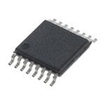
| 描述 | IC ENCODER PROG 10-BIT 16-SSOP |
| 产品分类 | 磁性传感器 - 霍尔效应,数字开关,线性,罗盘 (IC) |
| 品牌 | ams |
| 数据手册 | http://www.ams.com/eng/content/download/7333/116570 |
| 产品图片 |
|
| 产品型号 | AS5140H-ASSM |
| rohs | 无铅 / 符合限制有害物质指令(RoHS)规范要求 |
| 产品系列 | - |
| 产品培训模块 | http://www.digikey.cn/PTM/IndividualPTM.page?site=cn&lang=zhs&ptm=26195 |
| 供应商器件封装 | 16-SSOP |
| 其它名称 | AS5140H-ASSMTR |
| 包装 | 带卷 (TR) |
| 封装/外壳 | 16-SSOP(0.209",5.30mm 宽) |
| 工作温度 | -40°C ~ 150°C |
| 应用说明 | http://www.austriamicrosystems.com/eng/content/view/download/11922http://www.austriamicrosystems.com/eng/content/view/download/11921 |
| 感应范围 | 45mT ~ 75mT |
| 标准包装 | 500 |
| 特性 | 可编程 |
| 特色产品 | http://www.digikey.com/product-highlights/cn/zh/austriamicrosystems-as5140-automotive-encoder/1065 |
| 电压-电源 | 3 V ~ 3.6 V,4.5 V ~ 5.5 V |
| 电流-电源 | 16mA |
| 电流-输出(最大值) | 4mA |
| 类型 | 线性,旋转编码器 - 可编程 |
| 输出类型 | 数字式,PWM,10 位串行 |


- 商务部:美国ITC正式对集成电路等产品启动337调查
- 曝三星4nm工艺存在良率问题 高通将骁龙8 Gen1或转产台积电
- 太阳诱电将投资9.5亿元在常州建新厂生产MLCC 预计2023年完工
- 英特尔发布欧洲新工厂建设计划 深化IDM 2.0 战略
- 台积电先进制程称霸业界 有大客户加持明年业绩稳了
- 达到5530亿美元!SIA预计今年全球半导体销售额将创下新高
- 英特尔拟将自动驾驶子公司Mobileye上市 估值或超500亿美元
- 三星加码芯片和SET,合并消费电子和移动部门,撤换高东真等 CEO
- 三星电子宣布重大人事变动 还合并消费电子和移动部门
- 海关总署:前11个月进口集成电路产品价值2.52万亿元 增长14.8%


PDF Datasheet 数据手册内容提取
AS5140H 10-Bit 360º Programmable Magnetic Rotary Encoder For High Ambient Temperatures General Description The AS5140H is a contactless magnetic rotary encoder for accurate angular measurement over a full turn of 360º and over an extended ambient temperature range of -40ºC to 150ºC. It is a system-on-chip, combining integrated Hall elements, analog front end and digital signal processing in a single device. To measure the angle, only a simple two-pole magnet, rotating over the center of the chip, is required. The magnet may be placed above or below the IC. The absolute angle measurement provides instant indication of the magnet’s angular position with a resolution of 0.35º = 1024 positions per revolution. This digital data is available as a serial bit stream and as a PWM signal. Furthermore, a user-programmable incremental output is available. An internal voltage regulator allows the AS5140H to operate at either 3.3V or 5V supplies. The AS5140H is pin-compatible to the AS5040; however it uses low-voltage OTP programming cells with additional programming options. OrderingInformation and ContentGuide appear at end of datasheet. Key Benefits & Features The benefits and features of AS5140H, 10-Bit 360º Programmable Magnetic Rotary Encoder For High Ambient Temperatures are listed below: Figure 1: Added Value of Using AS5140H Benefits Features Contactless high resolution rotational position encoding over a No mechanical wear full turn of 360º Two digital 10-bit absolute outputs: Serial interface and Pulse High resolution absolute position sensing width modulated (PWM) output Three incremental output modes: Quadrature A/B and Index Easy to use for motor control output signal, Step / Direction and Index output signal, 3-phase commutation for brushless DC motors Adjustable zero position User programmable zero / index position ams Datasheet Page 1 [v1-09] 2018-Feb-20 DocumentFeedback
AS5140H − General Description Benefits Features Failure detection mode for magnet placement monitoring and Tolerant to magnet misalignment loss of power supply Usable for high speed applications Rotational speeds up to 10000 rpm Pushbutton functionality detects movement of magnet in Tolerant to airgap variations Z-axis Serial read-out of multiple interconnected AS5140H devices Supports daisy chain application using Daisy Chain mode Fitting to automotive applications Fully automotive qualified to AEC-Q100, grade 0 Operates up to 150°C ambient temperature Wide ambient temperature range: -40ºC to 150ºC Applications The AS5140H is an ideal solution for automotive applications like engine compartment sensors, transmission gearbox encoder, throttle valve position control and for industrial applications like rotary sensors in high temperature environment. Block Diagram The functional blocks of this device for reference are shown below: Figure 2: AS5140H Block Diagram (cid:57)(cid:39)(cid:39)(cid:57)(cid:22)(cid:57) (cid:48)(cid:68)(cid:74)(cid:44)(cid:49)(cid:38)(cid:81) (cid:57)(cid:39)(cid:39)(cid:24)(cid:57) LDO 3.3V (cid:48)(cid:68)(cid:74)(cid:39)(cid:40)(cid:38)(cid:81) PWM (cid:51)(cid:58)(cid:48)(cid:66)(cid:47)(cid:54)(cid:37) Interface (cid:54)(cid:76)(cid:81) (cid:36)(cid:81)(cid:74) DSP Absolute (cid:39)(cid:50) Hall Array (cid:38)(cid:82)(cid:86) (cid:48)(cid:68)(cid:74) Interface (cid:38)(cid:54)(cid:81) & (SSI) Frontend (cid:38)(cid:47)(cid:46) Amplifier OTP Register (cid:36)(cid:66)(cid:47)(cid:54)(cid:37)(cid:66)(cid:56) Incremental Programming Interface (cid:37)(cid:66)(cid:39)(cid:76)(cid:85)(cid:66)(cid:57) AS5140H Parameters (cid:44)(cid:81)(cid:71)(cid:72)(cid:91)(cid:66)(cid:58) (cid:51)(cid:85)(cid:82)(cid:74) Page 2 ams Datasheet DocumentFeedback [v1-09] 2018-Feb-20
AS5140H − Pin Assignment Pin Assignment Figure 3: Pin Diagram (Top View) (cid:48)(cid:68)(cid:74)(cid:44)(cid:49)(cid:38)(cid:81) (cid:20) (cid:20)(cid:25) (cid:57)(cid:39)(cid:39)(cid:24)(cid:57) (cid:48)(cid:68)(cid:74)(cid:39)(cid:40)(cid:38)(cid:81) (cid:21) (cid:20)(cid:24) (cid:57)(cid:39)(cid:39)(cid:22)(cid:57)(cid:22) (cid:36)(cid:66)(cid:47)(cid:54)(cid:37)(cid:66)(cid:56) (cid:22) (cid:20)(cid:23) (cid:49)(cid:38) A (cid:37)(cid:66)(cid:39)(cid:76)(cid:85)(cid:66)(cid:57) (cid:23) S (cid:20)(cid:22) (cid:49)(cid:38) 5 1 (cid:49)(cid:38) (cid:24) 4 (cid:20)(cid:21) (cid:51)(cid:58)(cid:48)(cid:66)(cid:47)(cid:54)(cid:37) 0 H (cid:44)(cid:81)(cid:71)(cid:72)(cid:91)(cid:66)(cid:58)(cid:3) (cid:25) (cid:20)(cid:20) (cid:38)(cid:54)(cid:81) (cid:57)(cid:54)(cid:54) (cid:26) (cid:20)(cid:19) (cid:38)(cid:47)(cid:46) (cid:51)(cid:85)(cid:82)(cid:74) (cid:27) (cid:28) (cid:39)(cid:50) Pin Description The following figure shows the description of each pin of the standard SSOP16 package (Shrink Small Outline Package, 16 leads, body size: 5.3mm x 6.2mmm; See Figure3). Figure 4: Pin Description Pin Number Pin Name Description Magnet Field Magnitude Increase. Active low. Indicates a distance 1 MagINCn reduction between the magnet and the device surface. Magnet Field Magnitude Decrease. Active low. Indicates a distance 2 MagDECn increase between the device and the magnet. Mode1.x: Quadrature A channel 3 A_LSB_U Mode2.x: Least Significant Bit Mode3.x: U signal (phase1) Mode1.x: Quadrature B channel quarter period shift to channel A 4 B_Dir_V Mode2.x: Direction of Rotation Mode3.x: V signal (phase2) 5 NC For internal use. Must be left unconnected. Mode1.x and Mode2.x: Index signal indicates the absolute zero position 6 Index_ W Mode3.x: W signal (phase3) ams Datasheet Page 3 [v1-09] 2018-Feb-20 DocumentFeedback
AS5140H − Pin Assignment Pin Number Pin Name Description 7 VSS Negative Supply Voltage (GND). OTP Programming Input and Data Input for Daisy Chain mode. Internal 8 Prog pull-down resistor (~74kΩ). May be connected to VSS if programming is not used. 9 DO Data Output of Synchronous Serial Interface. 10 CLK SSI Clock Input. Schmitt-Trigger input. Chip Select. Active low; Schmitt-Trigger input, internal pull-up resistor 11 CSn (~50kΩ) connect to VSS in incremental mode (see Incremental Power-up Lock Option on page 21) 12 PWM_LSB Pulse Width Modulation of approx. 1kHz; LSB in Mode3.x 13 NC For internal use. Must be left unconnected. 14 NC For internal use. Must be left unconnected. 15 VDD3V3 3V-Regulator Output (see Figure38) 16 VDD5V Positive Supply Voltage 5V Pin 1 and 2 are the magnetic field change indicators, MagINCn and MagDECn (magnetic field strength increase or decrease through variation of the distance between the magnet and the device). These outputs can be used to detect the valid magnetic field range. Furthermore those indicators can also be used for contact-less push-button functionality. Pins 3, 4 and 6 are the incremental pulse output pins. The functionality of these pins can be configured through programming the one-time programmable (OTP) register. Figure 5: Pin Assignment for Different Incremental Output Modes Output Mode Pin 3 Pin 4 Pin 6 Pin 12 1.x: Quadrature A B Index PWM 2.x: Step/direction LSB Direction Index PWM 3.x: Commutation U V W LSB Mode 1.x: Quadrature A/B Output Represents the default quadrature A/B signal mode. Mode 2.x: Step / Direction Output Configures pin 3 to deliver up to 512 pulses (up to 1024 state changes) per revolution. It is equivalent to the LSB (least significant bit) of the absolute position value. Pin 4 provides the information of the rotational direction. Page 4 ams Datasheet DocumentFeedback [v1-09] 2018-Feb-20
AS5140H − Pin Assignment Note(s): Both modes (mode 1.x and mode 2.x) provide an index signal (1 pulse/revolution) with an adjustable width of one LSB or three LSB’s. Mode 3.x: Brushless DC Motor Commutation Mode In addition to the absolute encoder output over the SSI interface, this mode provides commutation signals for brushless DC motors with either one pole pair or two pole pair rotors. The commutation signals are usually provided by 3 discrete Hall switches, which are no longer required, as the AS5140H can fulfill two tasks in parallel: absolute encoder + BLDC motor commutation. In this mode, • Pin 12 provides the LSB output instead of the PWM (Pulse-Width-Modulation) signal. • Pin 8 (Prog) is also used to program the different incremental interface modes, the incremental resolution and the zero position into the OTP (see Incremental Mode Programming). This pin is also used as digital input to shift serial data through the device in Daisy Chain configuration, (see Figure24). • Pin 11 Chip Select (CSn; active low) selects a device within a network of AS5140H encoders and initiates serial data transfer. A logic high at CSn puts the data output pin (DO) to tri-state and terminates serial data transfer. This pin is also used for alignment mode (see Alignment Mode) and programming mode (see Programming the AS5140H). • Pin 12 allows a single wire output of the 10-bit absolute position value. The value is encoded into a pulse width modulated signal with 1μs pulse width per step (1μs to 1024μs over a full turn). By using an external low pass filter, the digital PWM signal is converted into an analog voltage, allowing a direct replacement of potentiometers. ams Datasheet Page 5 [v1-09] 2018-Feb-20 DocumentFeedback
AS5140H − Absolute Maximum Ratings Absolute Maximum Ratings Stresses beyond those listed in Absolute maximum Ratings may cause permanent damage to the device. These are stress ratings only, and functional operation of the device at these or any other conditions beyond those indicated in Operating Conditions is not implied. Exposure to absolute maximum rating conditions for extended periods may affect device reliability. Figure 6: Absolute Maximum Ratings Parameter Min Max Units Comments DC supply voltage at pin VDD5V -0.3 7 V DC supply voltage at pin VDD3V3 -0.3 5 V Input pin voltage -0.3 7 V Pins Prog, MagINCn, MagDECn, CLK, CSn Input current (latchup immunity) -100 100 mA Norm: JEDEC 78 Electrostatic discharge ± 2 kV Norm: MIL 883 E method 3015 Storage temperature -55 150 ºC Body temperature t=20 to 40s, Norm: IPC/JEDEC J-Std-020C 260 ºC (Lead-free package) Lead finish 100% Sn “matte tin” Humidity non-condensing 5 85 % Ambient temperature -40 150 ºC Represents a maximum floor time of Moisture Sensitivity Level (MSL) 3 168h Page 6 ams Datasheet DocumentFeedback [v1-09] 2018-Feb-20
AS5140H − Electrical Characteristics Electrical Characteristics T = -40 to 150ºC, VDD5V = 3.0-3.6V (3V operation) AMB VDD5V = 4.5-5.5V (5V operation) unless otherwise noted. Figure 7: Operating Conditions Symbol Parameter Condition Min Typ Max Unit I Supply current 16 21 mA supp External supply voltage at VDD5V 4.5 5.0 5.5 V pin VDD5V 5V operation Internal regulator output VDD3V3 3.0 3.3 3.6 V voltage at pin VDD3V3 VDD5V 3.3V operation 3.0 3.3 3.6 V External supply voltage at (pins VDD5V and VDD3V3 pin VDD5V, VDD3V3 VDD3V3 connected) 3.0 3.3 3.6 V External VDD3V3 supply 10-90% level in 3.3V mode t voltage rise time at (pins VDD5V and VDD3V3 1 150 μs pwrup3 power-up connected) DC Characteristics for Digital Inputs and Outputs Figure 8: CMOS Schmitt-Trigger Inputs: CLK, CSn (CSn = Internal Pull-up) Symbol Parameter Condition Min Typ Max Unit V High level input voltage Normal operation 0.7 *VDD5V V IH V Low level input voltage 0.3 *VDD5V V IL V - V Schmitt Trigger hysteresis 1 V ION IOFF I Input leakage current CLK only -1 1 LEAK μA Pull-up low level input CSn only, I -30 -100 iL current VDD5V:5.0V ams Datasheet Page 7 [v1-09] 2018-Feb-20 DocumentFeedback
AS5140H − Electrical Characteristics Figure 9: CMOS / Program Input: Prog Symbol Parameter Condition Min Typ Max Unit V High level input voltage 0.7 *VDD5V 5 V IH During Refer to V High level input voltage V PROG programming Programming Conditions V Low level input voltage 0.3 *VDD5V V IL Pull-up high level input I VDD5V:5.0V 100 μA iL current Figure 10: CMOS Output Open Drain: MagINCn, MagDECn Symbol Parameter Condition Min Typ Max Unit V Low level output voltage VSS+0.4 V OL VDD5V:4.5V 4 I Output current mA O VDD5V:3V 2 Open drain leakage I 1 μA OZ current Figure 11: CMOS Output: A, B, Index, PWM Symbol Parameter Condition Min Typ Max Unit V High level output voltage VDD5V-0.5 V OH V Low level output voltage VSS+0.4 V OL VDD5V:4.5V 4 I Output current mA O VDD5V:3V 2 Page 8 ams Datasheet DocumentFeedback [v1-09] 2018-Feb-20
AS5140H − Electrical Characteristics Figure 12: Tristate CMOS Output: DO Symbol Parameter Condition Min Typ Max Unit V High level output voltage VDD5V-0.5 V OH V Low level output voltage VSS+0.4 V OL VDD5V:4.5V 4 I Output current mA O VDD5V:3V 2 I Tri-state leakage current 1 μA OZ Magnetic Input Specification Figure 13: Electrical Characteristics Symbol Parameter Condition Min Typ Max Unit Magnetic Input Specification (Two-pole cylindrical diametrically magnetized source) d Diameter Recommended magnet: 4 6 mag Ø 6mm x 2.5mm for cylindrical mm t Thickness magnets 2.5 mag Required vertical component of the magnetic field strength Magnetic input field B on the die’s surface, measured 45 75 mT pk amplitude along a concentric circle with a radius of 1.1mm B Magnetic offset Constant magnetic stray field ± 10 mT OFF Field non-linearity Including offset gradient 5 % Absolute mode: 600 rpm @ readout of 1024 positions 10 (see Figure33) Input frequency f (rotational speed of Hz mag_abs Incremental mode: no missing magnet) pulses at rotational speeds of 166 up to 10000 rpm (see Figure33) Max. X-Y offset between defined IC package center and 0.25 magnet axis (see Figure40) Disp Displacement radius mm Max. X-Y offset between chip 0.485 center and magnet axis ams Datasheet Page 9 [v1-09] 2018-Feb-20 DocumentFeedback
AS5140H − Electrical Characteristics Symbol Parameter Condition Min Typ Max Unit Placement tolerance of chip Chip placement within IC package ±0.235 mm tolerance (see Figure42) NdFeB (Neodymium Iron Recommended -0.12 Boron) magnet material and %/K temperature drift SmCo (Samarium Cobalt) -0.035 Electrical System Specifications Figure 14: Electrical System Specifications Symbol Parameter Condition Min Typ Max Unit RES Resolution(1) 0.352 deg 10 bit 7 bit 2.813 Adjustable resolution only 8 bit 1.406 available for incremental LSB deg output modes; Least 9 bit 0.703 significant bit, minimum step 10 bit 0.352 Maximum error with respect to Integral non-linearity the best line fit. Verified at INL ±0.5 deg opt (optimum)(2) optimum magnet placement, T =25ºC AMB Maximum error with respect to Integral non-linearity the best line fit. Verified at INL ±0.9 deg temp optimum magnet placement, (optimum) T = -40ºC to 150ºC AMB Best line fit = (Err – Err ) / 2 max min Over displacement tolerance INL Integral non-linearity ±1.4 deg with 6mm diameter magnet, TAMB = -40ºC to 150ºC (see Figure19) Differential DNL 10bit, no missing codes ±0.176 deg non-linearity(3) Deg TN Transition noise(4) RMS equivalent to 1 sigma 0.12 RMS Hyst Hysteresis Incremental modes only 0.704 deg Page 10 ams Datasheet DocumentFeedback [v1-09] 2018-Feb-20
AS5140H − Electrical Characteristics Symbol Parameter Condition Min Typ Max Unit Power-on reset thresholds V 1.37 2.2 2.9 ON On voltage; 300mV typ. hysteresis DC supply voltage 3.3V V (VDD3V3) Power-on reset thresholds V 1.08 1.9 2.6 OFF OFF voltage; 300mV typ. hysteresis Until offset compensation t Power-up time 50 ms PwrUp finished System propagation t Includes delay of ADC and DSP 48 μs delay delay absolute output System propagation delay incremental Calculation over two samples 192 μs output Internal sampling rate, 9.90 10.42 10.94 T = 25ºC Sampling rate for AMB fS absolute output kHz Internal sampling rate, 9.38 10.42 11.46 T = -40ºC to 150ºC AMB Max. clock frequency to read CLK Read-out frequency 1 MHz out serial data Note(s) and/or Footnote(s): 1. Digital Interface. 2. Integral Non-Linearity (INL) is the maximum deviation between actual position and indicated position. 3. Differential Non-Linearity (DNL) is the maximum deviation of the step length from one position to the next. 4. Transition Noise (TN) is the repeatability of an indicated position. ams Datasheet Page 11 [v1-09] 2018-Feb-20 DocumentFeedback
AS5140H − Electrical Characteristics Programming Conditions T = -40ºC to 150ºC, VDD5V = 3.0-3.6V (3V operation) AMB VDD5V = 4.5-5.5V (5V operation), unless otherwise noted. Figure 15: Programming Conditions Symbol Parameter Condition Min Typ Max Unit Voltage applied during V Programming voltage 3.0 3.3 3.6 V PROG programming Programming voltage Line must be discharged to V 0 1 V ProgOFF OFF level this level Current during I Programming current 100 mA PROG programming Programmed fuse 10μA max. current @ R 100k Ω programmed resistance (log 1) 100mV Unprogrammed fuse R 2mA max. current @ 100mV 50 100 Ω unprogrammed resistance (log 0) Programming time per Time to prog. a single fuse t 10 20 μs PROG bit bit Time to charge the cap after t Refresh time per bit 1 μs CHARGE t PROG f LOAD frequency Data can be loaded at n*2μs 500 kHz LOAD f READ frequency Read the data from the latch 2.5 MHz READ f WRITE frequency Write the data to the latch 2.5 MHz WRITE Page 12 ams Datasheet DocumentFeedback [v1-09] 2018-Feb-20
AS5140H − Electrical Characteristics Timing Characteristics T = -40 to 150 ºC, VDD5V = 3.0 to 3.6V (3V operation) AMB VDD5V = 4.5 to 5.5V (5V operation), unless otherwise noted Figure 16: Synchronous Serial Interface (SSI) Unit Symbol Parameter Conditions Min Typ Max s Time between falling edge of Data output activated t CSn and data output 100 ns DO active (logic high) activated Time between falling edge of First data shifted to output t CSn and first falling edge of 500 ns CLKFE register CLK Rising edge of CLK shifts out T Start of data output 500 ns CLK/2 one bit at a time Time between rising edge of t Data output valid 413 ns DO valid CLK and data output valid After the last bit DO changes t Data output tristate 100 ns DO tristate back to “tri-state” CSn =high; to initiate read-out t Pulse width of CSn 500 ns CSn of next angular position Clock frequency to read out f Read-out frequency >0 1 MHz CLK serial data Figure 17: Pulse Width Modulation Output Symbol Parameter Conditions Min Typ Max Units Signal period = 1025μs ±5% at 0.927 0.976 1.024 T = 25ºC AMB f PWM frequency kHz PWM Signal period =1025μs ±10% 0.878 0.976 1.074 at T = -40ºC to 150ºC AMB PW Minimum pulse width Position 0d; angle 0 degree 0.90 1 1.10 μs MIN Position 1023d; angle 359.65 PW Maximum pulse width 922 1024 1126 μs MAX degree ams Datasheet Page 13 [v1-09] 2018-Feb-20 DocumentFeedback
AS5140H − Electrical Characteristics Figure 18: Incremental Outputs Symbol Parameter Conditions Min Typ Max Units Time between first falling t Incremental outputs valid edge of CSn after power-up Incremental 500 ns outputs valid after power-up and valid incremental outputs Time between rising or falling edge of LSB output t Directional indication valid 500 ns Dir valid and valid directional indication Figure 19: Integral and Differential Non-Linearity Example (Exaggerated Curve) 1023 (cid:68)(cid:20)(cid:19)(cid:69)(cid:76)(cid:87)(cid:3)(cid:70)(cid:82)(cid:71)(cid:72) 1023 (cid:36)(cid:70)(cid:87)(cid:88)(cid:68)(cid:79)(cid:3)(cid:70)(cid:88)(cid:85)(cid:89)(cid:72) 2 (cid:55)(cid:49) (cid:44)(cid:71)(cid:72)(cid:68)(cid:79)(cid:3)(cid:70)(cid:88)(cid:85)(cid:89)(cid:72) 1 (cid:39)(cid:49)(cid:47)(cid:14)(cid:20)(cid:47)(cid:54)(cid:37) 0 (cid:44)(cid:49)(cid:47) (cid:19)(cid:17)(cid:22)(cid:24)(cid:131) 512 512 0 0(cid:113) (cid:20)(cid:27)(cid:19)(cid:113) 360(cid:113) (cid:68)(cid:62)(cid:71)(cid:72)(cid:74)(cid:85)(cid:72)(cid:72)(cid:86)(cid:64) Page 14 ams Datasheet DocumentFeedback [v1-09] 2018-Feb-20
AS5140H − Detailed Description Detailed Description The AS5140H is manufactured in a CMOS standard process and uses a spinning current Hall technology for sensing the magnetic field distribution across the surface of the chip. The integrated Hall elements are placed around the center of the device, and deliver a voltage representation of the magnetic field at the surface of the IC. Through Sigma-Delta Analog / Digital Conversion and Digital Signal-Processing (DSP) algorithms, the AS5140H provides accurate high-resolution absolute angular position information. For this purpose, a Coordinate Rotation Digital Computer (CORDIC) calculates the angle and the magnitude of the Hall array signals. The DSP is also used to provide digital information at the outputs MagINCn and MagDECn that indicate movements of the used magnet towards or away from the device’s surface. A small low cost diametrically magnetized (two-pole) standard magnet provides the angular position information (see Figure39). The AS5140H senses the orientation of the magnetic field and calculates a 10-bit binary code. This code can be accessed via a Synchronous Serial Interface (SSI). In addition, an absolute angular representation is given by a Pulse Width Modulated signal at pin 12 (PWM). Simultaneously, the device also provides incremental output signals. The various incremental output modes can be selected by programming the OTP mode register bits (see Figure35). As long as no programming voltage is applied to pin Prog, the new setting may be overwritten at any time and will be reset to default when power is turned off. To make the setting permanent, the OTP register must be programmed. The default setting is a quadrature A/B mode including the Index signal with a pulse width of 1 LSB. The Index signal is logic high at the user programmable zero position. The AS5140H is tolerant to magnet misalignment and magnetic stray fields due to differential measurement technique and Hall sensor conditioning circuitry. Figure 20: Typical Arrangement of AS5140H and Magnet ams Datasheet Page 15 [v1-09] 2018-Feb-20 DocumentFeedback
AS5140H − Detailed Description 10-Bit Absolute Angular Position Output Synchronous Serial Interface (SSI) If CSn changes to logic low, Data Out (DO) will change from high impedance (tri-state) to logic high and the read-out will be initiated. • After a minimum time t , data is latched into the CLK FE output shift register with the first falling edge of CLK. • Each subsequent rising CLK edge shifts out one bit of data. • The serial word contains 16 bits; the first 10 bits are the angular information D[9:0], the subsequent 6 bits contain system information about the validity of data such as OCF, COF, LIN, Parity and Magnetic Field status (increase/decrease). • A subsequent measurement is initiated by a log “high” pulse at CSn with a minimum duration of t . CSn Figure 21: Synchronous Serial Interface with Absolute Angular Position Data (cid:87)(cid:38)(cid:47)(cid:46)(cid:3)(cid:41)(cid:40) (cid:38)(cid:54)(cid:81) (cid:55)(cid:38)(cid:47)(cid:46)(cid:18)(cid:21) (cid:87)(cid:38)(cid:54)(cid:81) (cid:87)(cid:38)(cid:47)(cid:46)(cid:3)(cid:41)(cid:40) (cid:20) (cid:27) (cid:20)(cid:25) (cid:20) (cid:38)(cid:47)(cid:46) (cid:48)(cid:68)(cid:74) (cid:48)(cid:68)(cid:74) (cid:40)(cid:89)(cid:72)(cid:81) (cid:39)(cid:50) (cid:39)(cid:28) (cid:39)(cid:27) (cid:39)(cid:26) (cid:39)(cid:25) (cid:39)(cid:24) (cid:39)(cid:23) (cid:39)(cid:22) (cid:39)(cid:21) (cid:39)(cid:20) (cid:39)(cid:19) (cid:50)(cid:38)(cid:41) (cid:38)(cid:50)(cid:41) (cid:47)(cid:44)(cid:49) (cid:39)(cid:28) (cid:44)(cid:49)(cid:38) (cid:39)(cid:40)(cid:38) (cid:51)(cid:36)(cid:53) (cid:87)(cid:39)(cid:50)(cid:3)(cid:68)(cid:70)(cid:87)(cid:76)(cid:89)(cid:72) (cid:87)(cid:39)(cid:50)(cid:3)(cid:89)(cid:68)(cid:79)(cid:76)(cid:71) (cid:36)(cid:81)(cid:74)(cid:88)(cid:79)(cid:68)(cid:85)(cid:3)(cid:51)(cid:82)(cid:86)(cid:76)(cid:87)(cid:76)(cid:82)(cid:81)(cid:3)(cid:39)(cid:68)(cid:87)(cid:68) (cid:54)(cid:87)(cid:68)(cid:87)(cid:88)(cid:86)(cid:3)(cid:37)(cid:76)(cid:87)(cid:86) (cid:87)(cid:39)(cid:50)(cid:3)(cid:55)(cid:85)(cid:76)(cid:86)(cid:87)(cid:68)(cid:87)(cid:72) Data Content D9:D0 – Absolute angular position data (MSB is clocked out first). OCF – (Offset Compensation Finished). Logic high indicates the finished Offset Compensation Algorithm. For fast startup, this bit may be polled by the external microcontroller. As soon as this bit is set, the AS5140H has completed the startup and the data is valid (see Figure23). COF – (Cordic Overflow). Logic high indicates an out of range error in the CORDIC part. When this bit is set, the data at D9:D0 is invalid. The absolute output maintains the last valid angular value. This alarm may be resolved by bringing the magnet within the X-Y-Z tolerance limits. Page 16 ams Datasheet DocumentFeedback [v1-09] 2018-Feb-20
AS5140H − Detailed Description LIN – (Linearity Alarm). Logic high indicates that the input field generates a critical output linearity. When this bit is set, the data at D9:D0 may still be used, but can contain invalid data. This warning may be resolved by bringing the magnet within the X-Y-Z tolerance limits. MagINCn – (Magnitude Increase) becomes HIGH, when the magnet is pushed towards the IC, thus increasing the magnetic field strength. MagDECn – (Magnitude Decrease) becomes HIGH, when the magnet is pulled away from the IC, thus decreasing the magnetic field strength. Signal “HIGH” for both MagINCn and MagDECn indicate a magnetic field that is out of the allowed range (see Figure22). Figure 22: Magnetic Magnitude Variation Indicator MagINCn MagDECn Description No distance change 0 0 Magnetic Input Field OK (in range) Distance increase: Pull-function. This state is dynamic, it is 0 1 only active while the magnet is moving away from the chip in Z-axis. Distance decrease: Push- function. This state is dynamic, it is 1 0 only active while the magnet is moving towards the chip in Z-axis. Magnetic Input Field invalid – out of range: Too large, too 1 1 small (missing magnet). Note(s) and/or Footnote(s): 1. Pins 1 and 2 (MagINCn, MagDECn) are open drain outputs and require external pull-up resistors. If the magnetic field is in range, both outputs are turned OFF. The two pins may also be combined with a single pull-up resistor. In this case, the signal is high when the magnetic field is in range. It is low in all other cases (see Figure22). Even Parity – A bit for transmission error detection of bits 1to 15 (D9 to D0, OCF, COF, LIN, MagINCn, MagDECn). The absolute angular output is always set to a resolution of 10 bit. Placing the magnet above the chip, angular values increase in clockwise direction by default. Data D9:D0 is valid, when the status bits have the following configurations: ams Datasheet Page 17 [v1-09] 2018-Feb-20 DocumentFeedback
AS5140H − Detailed Description Figure 23: Status Bit Outputs OCF COF LIN MagINCn MagDECn Parity 0 0 1 0 0 0 1 Even checksum of bits 1:15 1 0 The absolute angular position is sampled at a rate of 10kHz (0.1ms). This allows reading of all 1024 positions per 360 degrees within 0.1 seconds = 9.76Hz (~10Hz) without skipping any position. Multiplying 10Hz by 60, results the corresponding maximum rotational speed of 600rpm. Readout of every second angular position allows for rotational speeds of up to 1200 rpm. Consequently, increasing the rotational speed reduces the number of absolute angular positions per revolution (see Figure45). Regardless of the rotational speed or the number of positions to be read out, the absolute angular value is always given at the highest resolution of 10 bit. The incremental outputs are not affected by rotational speed restrictions due to the implemented interpolator. The incremental output signals may be used for high-speed applications with rotational speeds of up to 10000 rpm without missing pulses. Daisy Chain Mode The Daisy Chain mode allows connection of several AS5140H’s in series, while still keeping just one digital input for data transfer (see “Data IN” in Figure24 below). This mode is accomplished by connecting the data output (DO; pin 9) to the data input (Prog; pin 8) of the subsequent device. The serial data of all connected devices is read from the DO pin of the first device in the chain. The Prog pin of the last device in the chain should be connected to VSS. The length of the serial bit stream increases with every connected device. It is, (EQ1) n * (16+1) bits For example, 34 bits for two devices, 51 bits for three devices, etc. The last data bit of the first device (Parity) is followed by a logic low bit and the first data bit of the second device (D9), etc. (see Figure25). Page 18 ams Datasheet DocumentFeedback [v1-09] 2018-Feb-20
AS5140H − Detailed Description Figure 24: Daisy Chain Hardware Configuration AS5140H AS5140H AS5140H µC 1st Device 2nd Device last Device (cid:39)(cid:68)(cid:87)(cid:68)(cid:3)(cid:44)(cid:49) (cid:39)(cid:50) (cid:51)(cid:85)(cid:82)(cid:74) (cid:39)(cid:50) (cid:51)(cid:85)(cid:82)(cid:74) (cid:39)(cid:50) (cid:51)(cid:85)(cid:82)(cid:74) (cid:38)(cid:54)(cid:81) (cid:38)(cid:47)(cid:46) (cid:38)(cid:54)(cid:81) (cid:38)(cid:47)(cid:46) (cid:38)(cid:54)(cid:81) (cid:38)(cid:47)(cid:46) (cid:38)(cid:47)(cid:46) (cid:38)(cid:54)(cid:81) Figure 25: Daisy Chain Mode Data Transfer (cid:38)(cid:54)(cid:81) (cid:55)(cid:38)(cid:47)(cid:46)(cid:18)(cid:21) (cid:87)(cid:38)(cid:47)(cid:46)(cid:3)(cid:41)(cid:40) (cid:20) (cid:27) (cid:20)(cid:25) (cid:39) (cid:20) (cid:21) (cid:22) (cid:38)(cid:47)(cid:46) (cid:48)(cid:68)(cid:74) (cid:48)(cid:68)(cid:74) (cid:40)(cid:89)(cid:72)(cid:81) (cid:39)(cid:50) (cid:39)(cid:28) (cid:39)(cid:27) (cid:39)(cid:26) (cid:39)(cid:25) (cid:39)(cid:24) (cid:39)(cid:23) (cid:39)(cid:22) (cid:39)(cid:21) (cid:39)(cid:20) (cid:39)(cid:19) (cid:50)(cid:38)(cid:41) (cid:38)(cid:50)(cid:41) (cid:47)(cid:44)(cid:49) (cid:39)(cid:28) (cid:39)(cid:27) (cid:39)(cid:26) (cid:44)(cid:49)(cid:38) (cid:39)(cid:40)(cid:38) (cid:51)(cid:36)(cid:53) (cid:87)(cid:39)(cid:50)(cid:3)(cid:68)(cid:70)(cid:87)(cid:76)(cid:89)(cid:72) (cid:87)(cid:39)(cid:50)(cid:3)(cid:89)(cid:68)(cid:79)(cid:76)(cid:71) (cid:36)(cid:81)(cid:74)(cid:88)(cid:79)(cid:68)(cid:85)(cid:3)(cid:51)(cid:82)(cid:86)(cid:76)(cid:87)(cid:76)(cid:82)(cid:81)(cid:3)(cid:39)(cid:68)(cid:87)(cid:68) (cid:54)(cid:87)(cid:68)(cid:87)(cid:88)(cid:86)(cid:3)(cid:37)(cid:76)(cid:87)(cid:86) (cid:36)(cid:81)(cid:74)(cid:88)(cid:79)(cid:68)(cid:85)(cid:3)(cid:51)(cid:82)(cid:86)(cid:76)(cid:87)(cid:76)(cid:82)(cid:81)(cid:3)(cid:39)(cid:68)(cid:87)(cid:68) (cid:20)(cid:86)(cid:87)(cid:3)(cid:39)(cid:72)(cid:89)(cid:76)(cid:70)(cid:72) (cid:21)(cid:81)(cid:71)(cid:3)(cid:39)(cid:72)(cid:89)(cid:76)(cid:70)(cid:72) Programming Daisy Chained Devices. In Daisy Chain mode, the Prog pin is connected directly to the DO pin of the subsequent device in the chain (see Figure24). During programming (see Programming the AS5140H), a programming voltage of 7.5V must be applied to pin Prog. This voltage level exceeds the limits for pin DO, so one of the following precautions must be made during programming: • Open the connection DO→Prog during programming, (or) • Add a Schottky diode between DO and Prog (Anode = DO, Cathode = Prog) Due to the parallel connection of CLK and CSn, all connected devices may be programmed simultaneously. ams Datasheet Page 19 [v1-09] 2018-Feb-20 DocumentFeedback
AS5140H − Detailed Description Incremental Outputs Three different incremental output modes are possible with quadrature A/B being the default mode. Figure26 shows the two-channel quadrature as well as the step / direction incremental signal (LSB) and the direction bit in clockwise (CW) and counter-clockwise (CCW) direction. Quadrature A/B Output (Quad A/B Mode) The phase shift between channel A and B indicates the direction of the magnet movement. Channel A leads channel B at a clockwise rotation of the magnet (top view) by 90 electrical degrees. Channel B leads channel A at a counter-clockwise rotation. Figure 26: Incremental Output Modes (cid:48)(cid:72)(cid:70)(cid:75)(cid:68)(cid:81)(cid:76)(cid:70)(cid:68)(cid:79) (cid:48)(cid:72)(cid:70)(cid:75)(cid:68)(cid:81)(cid:76)(cid:70)(cid:68)(cid:79) (cid:61)(cid:72)(cid:85)(cid:82)(cid:3)(cid:51)(cid:82)(cid:86)(cid:76)(cid:87)(cid:76)(cid:82)(cid:81) (cid:61)(cid:72)(cid:85)(cid:82)(cid:3)(cid:51)(cid:82)(cid:86)(cid:76)(cid:87)(cid:76)(cid:82)(cid:81) (cid:52)(cid:88)(cid:68)(cid:71)(cid:3)(cid:36)(cid:18)(cid:37)(cid:16)(cid:48)(cid:82)(cid:71)(cid:72) (cid:53)(cid:82)(cid:87)(cid:68)(cid:87)(cid:76)(cid:82)(cid:81)(cid:3)(cid:39)(cid:76)(cid:85)(cid:72)(cid:70)(cid:87)(cid:76)(cid:82)(cid:81) (cid:38)(cid:75)(cid:68)(cid:81)(cid:74)(cid:72) (cid:36) (cid:37) (cid:44)(cid:81)(cid:71)(cid:72)(cid:91)(cid:32)(cid:19) (cid:20)(cid:3)(cid:47)(cid:54)(cid:37) (cid:43)(cid:92)(cid:86)(cid:87)(cid:32) (cid:44)(cid:81)(cid:71)(cid:72)(cid:91) (cid:21)(cid:47)(cid:54)(cid:37) (cid:54)(cid:87)(cid:72)(cid:83)(cid:3)(cid:18)(cid:3)(cid:39)(cid:76)(cid:85)(cid:16)(cid:48)(cid:82)(cid:71)(cid:72) (cid:44)(cid:81)(cid:71)(cid:72)(cid:91)(cid:32)(cid:20) (cid:22)(cid:3)(cid:47)(cid:54)(cid:37) (cid:47)(cid:54)(cid:37) (cid:39)(cid:76)(cid:85) (cid:38)(cid:79)(cid:82)(cid:70)(cid:78)(cid:90)(cid:76)(cid:86)(cid:72)(cid:3)(cid:70)(cid:90) (cid:38)(cid:82)(cid:88)(cid:81)(cid:87)(cid:72)(cid:85)(cid:70)(cid:79)(cid:82)(cid:70)(cid:78)(cid:90)(cid:76)(cid:86)(cid:72)(cid:3)(cid:70)(cid:70)(cid:90) (cid:38)(cid:54)(cid:81) (cid:87)(cid:39)(cid:76)(cid:85)(cid:3)(cid:89)(cid:68)(cid:79)(cid:76)(cid:71) (cid:87)(cid:44)(cid:81)(cid:70)(cid:85)(cid:72)(cid:80)(cid:72)(cid:81)(cid:87)(cid:68)(cid:79)(cid:3)(cid:82)(cid:88)(cid:87)(cid:83)(cid:88)(cid:87)(cid:86)(cid:3)(cid:89)(cid:68)(cid:79)(cid:76)(cid:71) Page 20 ams Datasheet DocumentFeedback [v1-09] 2018-Feb-20
AS5140H − Detailed Description LSB Output (Step/Direction Mode) Output LSB reflects the LSB (least significant bit) of the programmed incremental resolution (OTP Register Bit Div0, Div1). Output Dir provides information about the rotational direction of the magnet, which may be placed above or below the device (1=clockwise; 0=counter clockwise; top view). Dir is updated with every LSB change. In both modes (quad A/B, step/direction), the resolution and the index output are user programmable. The index pulse indicates the zero position and is by default one angular step (1LSB) wide. However, it can be set to three LSBs by programming the Index-bit of the OTP register accordingly (seeFigure35). Incremental Power-up Lock Option. After power-up, the incremental outputs can optionally be locked or unlocked, depending on the status of the CSn pin: • CSn = low at power-up: CSn has an internal pull-up resistor and must be externally pulled low (R ≤ 5KΩ). If Csn is ext low at power-up, the incremental outputs (A, B, Index) will be high until the internal offset compensation is finished. This unique state (A=B=Index = high) may be used as an indicator for the external controller to shorten the waiting time at power-up. Instead of waiting for the specified maximum power up-time (0), the controller can start requesting data from the AS5140H as soon as the state (A=B=Index = high) is cleared. • CSn = high or open at power-up: In this mode, the incremental outputs (A, B, Index) will remain at logic high state, until CSn goes low or a low pulse is applied at CSn. This mode allows intentional disabling of the incremental outputs until, for example the system microcontroller is ready to receive data. Incremental Output Hysteresis To avoid flickering incremental outputs at a stationary magnet position, a hysteresis is introduced. In case of a rotational direction change, the incremental outputs have a hysteresis of 2 LSB. Regardless of the programmed incremental resolution, the hysteresis of 2 LSB always corresponds to the highest resolution of 10 bit. In absolute terms, the hysteresis is set to 0.704 degrees for all resolutions. For constant rotational directions, every magnet position change is indicated at the incremental outputs (see Figure27). For example, if the magnet turns clockwise from position “x+3“ to “x+4“, the incremental output would also indicate this position accordingly. A change of the magnet’s rotational direction back to position “x+3” means that the incremental output still remains unchanged for the duration of 2 LSB, until position “x+2” is reached. Following this direction, the incremental outputs will again be updated with every change of the magnet position. ams Datasheet Page 21 [v1-09] 2018-Feb-20 DocumentFeedback
AS5140H − Detailed Description Figure 27: Hysteresis Window for Incremental Outputs (cid:44)(cid:81)(cid:70)(cid:85)(cid:72)(cid:80)(cid:72)(cid:81)(cid:87)(cid:68)(cid:79) (cid:50)(cid:88)(cid:87)(cid:83)(cid:88)(cid:87) (cid:43)(cid:92)(cid:86)(cid:87)(cid:72)(cid:85)(cid:72)(cid:86)(cid:76)(cid:86)(cid:29)(cid:3) (cid:44)(cid:81)(cid:71)(cid:76)(cid:70)(cid:68)(cid:87)(cid:76)(cid:82)(cid:81) (cid:19)(cid:17)(cid:26)(cid:158) (cid:59)(cid:14)(cid:23) (cid:59)(cid:14)(cid:22) (cid:59)(cid:14)(cid:21) (cid:59)(cid:14)(cid:20) (cid:59) (cid:48)(cid:68)(cid:74)(cid:81)(cid:72)(cid:87)(cid:3)(cid:51)(cid:82)(cid:86)(cid:76)(cid:87)(cid:76)(cid:82)(cid:81) (cid:59) (cid:59)(cid:14)(cid:20) (cid:59)(cid:14)(cid:21) (cid:59)(cid:14)(cid:22) (cid:59)(cid:14)(cid:23) (cid:59)(cid:14)(cid:24) (cid:38)(cid:79)(cid:82)(cid:70)(cid:78)(cid:90)(cid:76)(cid:86)(cid:72)(cid:3)(cid:39)(cid:76)(cid:85)(cid:72)(cid:70)(cid:87)(cid:76)(cid:82)(cid:81) (cid:38)(cid:82)(cid:88)(cid:81)(cid:87)(cid:72)(cid:85)(cid:70)(cid:79)(cid:82)(cid:70)(cid:78)(cid:90)(cid:76)(cid:86)(cid:72)(cid:3)(cid:39)(cid:76)(cid:85)(cid:72)(cid:70)(cid:87)(cid:76)(cid:82)(cid:81) Pulse Width Modulation (PWM) Output The AS5140H provides a pulse width modulated output (PWM), whose duty cycle is proportional to the measured angle: t ⋅1025 (EQ2) Position = -----O----N----------------------–1 (t +t ) ON OFF The PWM frequency is internally trimmed to an accuracy of ±5% (±10% over full temperature range). This tolerance can be cancelled by measuring the complete duty cycle as shown above. Figure 28: PWM Output Signal (cid:36)(cid:81)(cid:74)(cid:79)(cid:72) (cid:51)(cid:58)(cid:48)(cid:44)(cid:49) (cid:19)(cid:3)(cid:71)(cid:72)(cid:74) (cid:11)(cid:51)(cid:82)(cid:86)(cid:3)(cid:19)(cid:12) (cid:20)(cid:151)(cid:86) (cid:20)(cid:19)(cid:21)(cid:24)(cid:151)(cid:86) (cid:51)(cid:58)(cid:48)(cid:36)(cid:59) (cid:22)(cid:24)(cid:28)(cid:17)(cid:25)(cid:24)(cid:3)(cid:71)(cid:72)(cid:74) (cid:11)(cid:51)(cid:82)(cid:86)(cid:3)(cid:20)(cid:19)(cid:21)(cid:22)(cid:12) (cid:20)(cid:19)(cid:21)(cid:23)(cid:151)(cid:86) (cid:20)(cid:18)(cid:73)(cid:51)(cid:58)(cid:48) Page 22 ams Datasheet DocumentFeedback [v1-09] 2018-Feb-20
AS5140H − Detailed Description Figure 29: PWM Signal Parameters Symbol Parameter Typ Unit Note f PWM frequency 0.9756 kHz Signal period: 1025μs PWM Position 0d PW MIN pulse width 1 μs MIN Angle 0 deg Position 1023d PW MAX pulse width 1024 μs MAX Angle 359.65 deg Analog Output An analog output may be generated by averaging the PWM signal, using an external active or passive lowpass filter. The analog output voltage is proportional to the angle: 0º = 0V; 360º = VDD5V. Using this method, the AS5140H can be used as direct replacement of potentiometers. Figure 30: Simple Passive 2nd Order Lowpass Filter (cid:53)(cid:20) (cid:53)(cid:21) (cid:68)(cid:81)(cid:68)(cid:79)(cid:82)(cid:74)(cid:3)(cid:82)(cid:88)(cid:87) (cid:51)(cid:76)(cid:81)(cid:20)(cid:21) (cid:51)(cid:58)(cid:48) (cid:57)(cid:39)(cid:39) (cid:38)(cid:20) (cid:38)(cid:21) (cid:19)(cid:57) (cid:51)(cid:76)(cid:81)(cid:26) (cid:19)(cid:158) (cid:22)(cid:25)(cid:19)(cid:158) (cid:57)(cid:54)(cid:54) (EQ3) R1, R2 ≥ 4k7 C1, C2 ≥ 1μF/6V R1 should be ≥4k7 to avoid loading of the PWM output. Larger values of Rx and Cx will provide better filtering and less ripple, but will also slow down the response time. ams Datasheet Page 23 [v1-09] 2018-Feb-20 DocumentFeedback
AS5140H − Detailed Description Brushless DC Motor Commutation Mode Brushless DC motors require angular information for stator commutation. The AS5140H provides U-V-W commutation signals for one and two pole pair motors. In addition to the three-phase output signals, the step (LSB) output at pin 12 allows high accuracy speed measurement. Two resolutions (9 or 10 bit) can be selected by programming Div0 according to Figure35. Mode 3.0 (3.1) is used for brush-less DC motors with one-pole pair rotors. The three phases (U, V, W) are 120 degrees apart, each phase is 180 degrees on and 180 degrees OFF. Mode 3.2 (3.3) is used for motors with two pole pairs requiring a higher pulse count to ensure a proper current commutation. In this case the pulse width is 256 positions, equal to 90 degrees. The precise physical angle at which the U, V and W signals change state (“Angle” in Figure31and Figure32) is calculated by multiplying each transition position by the angular value of 1 count: (EQ4) Angle[deg] = Position x (360 degree/1024) Figure 31: U, V and W-Signals for BLDC Motor Commutation (Div1=0, Div0=0) Commutation - Mode 3.0 (cid:11)(cid:50)(cid:81)(cid:72)(cid:16)(cid:83)(cid:82)(cid:79)(cid:72)(cid:16)(cid:83)(cid:68)(cid:76)(cid:85)(cid:12) (cid:58)(cid:76)(cid:71)(cid:87)(cid:75)(cid:3)(cid:29)(cid:3)(cid:24)(cid:20)(cid:21)(cid:3)(cid:54)(cid:87)(cid:72)(cid:83)(cid:86) (cid:58)(cid:76)(cid:71)(cid:87)(cid:75)(cid:3)(cid:29)(cid:3)(cid:24)(cid:20)(cid:21)(cid:3)(cid:54)(cid:87)(cid:72)(cid:83)(cid:86) (cid:56) (cid:57) (cid:58) (cid:38)(cid:58)(cid:3)(cid:39)(cid:76)(cid:85)(cid:72)(cid:70)(cid:87)(cid:76)(cid:82)(cid:81) (cid:51)(cid:82)(cid:86)(cid:76)(cid:87)(cid:76)(cid:82)(cid:81)(cid:29) (cid:19) (cid:20)(cid:26)(cid:20) (cid:22)(cid:23)(cid:20) (cid:24)(cid:20)(cid:21) (cid:25)(cid:27)(cid:22) (cid:27)(cid:24)(cid:22) (cid:19) (cid:36)(cid:81)(cid:74)(cid:79)(cid:72)(cid:29) (cid:19)(cid:17)(cid:19) (cid:25)(cid:19)(cid:17)(cid:20)(cid:21) (cid:20)(cid:20)(cid:28)(cid:17)(cid:27)(cid:27) (cid:20)(cid:27)(cid:19)(cid:17)(cid:19) (cid:21)(cid:23)(cid:19)(cid:17)(cid:20)(cid:21) (cid:21)(cid:28)(cid:28)(cid:17)(cid:27)(cid:27) (cid:22)(cid:25)(cid:19)(cid:17)(cid:19) Page 24 ams Datasheet DocumentFeedback [v1-09] 2018-Feb-20
AS5140H − Detailed Description Figure 32: U, V and W-Signals for 2Pole BLDC Motor Commutation (Div1=1, Div0=0) Commutation - Mode 3.2 (cid:11)(cid:55)(cid:90)(cid:82)(cid:16)(cid:83)(cid:82)(cid:79)(cid:72)(cid:16)(cid:83)(cid:68)(cid:76)(cid:85)(cid:86)(cid:12) (cid:58)(cid:76)(cid:71)(cid:87)(cid:75)(cid:3)(cid:29)(cid:3)(cid:21)(cid:24)(cid:25)(cid:3)(cid:54)(cid:87)(cid:72)(cid:83)(cid:86) (cid:58)(cid:76)(cid:71)(cid:87)(cid:75)(cid:3)(cid:29)(cid:3)(cid:21)(cid:24)(cid:25)(cid:3)(cid:54)(cid:87)(cid:72)(cid:83)(cid:86) (cid:56) (cid:57) (cid:58) (cid:38)(cid:58)(cid:3)(cid:39)(cid:76)(cid:85)(cid:72)(cid:70)(cid:87)(cid:76)(cid:82)(cid:81) (cid:51)(cid:82)(cid:86)(cid:76)(cid:87)(cid:76)(cid:82)(cid:81)(cid:29) (cid:19) (cid:27)(cid:24) (cid:20)(cid:26)(cid:20) (cid:21)(cid:24)(cid:25) (cid:22)(cid:23)(cid:20) (cid:23)(cid:21)(cid:26) (cid:24)(cid:20)(cid:21) (cid:24)(cid:28)(cid:26) (cid:25)(cid:27)(cid:22) (cid:26)(cid:25)(cid:27) (cid:27)(cid:24)(cid:22) (cid:28)(cid:22)(cid:28) (cid:19) (cid:36)(cid:81)(cid:74)(cid:79)(cid:72)(cid:29) (cid:19)(cid:17)(cid:19) (cid:21)(cid:28)(cid:17)(cid:27)(cid:27) (cid:25)(cid:19)(cid:17)(cid:20)(cid:21) (cid:28)(cid:19)(cid:17)(cid:19) (cid:20)(cid:20)(cid:28)(cid:17)(cid:27)(cid:27) (cid:20)(cid:24)(cid:19)(cid:17)(cid:20)(cid:21) (cid:20)(cid:27)(cid:19)(cid:17)(cid:19) (cid:21)(cid:19)(cid:28)(cid:17)(cid:27)(cid:27) (cid:21)(cid:23)(cid:19)(cid:17)(cid:20)(cid:21) (cid:21)(cid:26)(cid:19)(cid:17)(cid:19)(cid:19) (cid:21)(cid:28)(cid:28)(cid:17)(cid:27)(cid:27) (cid:22)(cid:22)(cid:19)(cid:17)(cid:20)(cid:21) (cid:22)(cid:25)(cid:19)(cid:17)(cid:19) Programming the AS5140H Note(s): A detailed description of the ams low voltage polyfuse OTP programming method is given in Application Note AN514X-10, which can be downloaded from the ams website. The OTP programming description in this datasheet is for general information only. After power-on, programming the AS5140H is enabled with the rising edge of CSn with Prog = high and CLK = low. The AS5140H programming is a one-time-programming (OTP) method, based on polysilicon fuses. The advantage of this method is that a programming voltage of only 3.3V is required for programming. The OTP consists of 52 bits, of which 21 bits are available for user programming. The remaining 31 bits contain factory settings and a unique chip identifier (Chip-ID). A single OTP cell can be programmed only once. Per default, the cell is “0”; a programmed cell will contain a “1”. While it is not possible to reset a programmed bit from “1” to “0”, multiple OTP writes are possible, as long as only unprogrammed “0”-bits are programmed to “1”. Independent of the OTP programming, it is possible to overwrite the OTP register temporarily with an OTP write command at any time. This setting will be cleared and overwritten with the hard programmed OTP settings at each power-up sequence or by a LOAD operation. ams Datasheet Page 25 [v1-09] 2018-Feb-20 DocumentFeedback
AS5140H − Detailed Description The OTP memory can be accessed in several ways: • Load Operation: The Load operation reads the OTP fuses and loads the contents into the OTP register. Note that the Load operation is automatically executed after each power-on-reset. • Write Operation: The Write operation allows a temporary modification of the OTP register. It does not program the OTP. This operation can be invoked multiple times, and will remain set while the chip is supplied with power and while the OTP register is not modified with another Write or Load operation. • Read Operation: The Read operation reads the contents of the OTP register, for example to verify a Write command or to read the OTP memory after a Load command. • Program Operation: The Program operation writes the contents of the OTP register permanently into the OTP ROM. • Analog Readback Operation: The Analog Readback operation allows a quantifiable verification of the programming. For each programmed or unprogrammed bit, there is a representative analog value (in essence, a resistor value) that is read to verify whether a bit has been successfully programmed or not. Page 26 ams Datasheet DocumentFeedback [v1-09] 2018-Feb-20
AS5140H − Detailed Description OTP Memory Assignment Figure 33: OTP Bit Assignment Bit Symbol Function mbit1 Factory Bit 1 51 Md0 50 Md1 49 Div0 Incremental output mode selection 48 Div1 47 Index n o ti 46 Z0 ec S r e : : 10-bit Zero Position m o t s 37 Z9 u C 36 CCW Direction 35 RA0 : : Redundancy Address 31 RA4 30 FS 0 n o ti c : : e Factory Bit S y r o 18 FS 12 ct a F 17 ChipID0 n 16 ChipID1 o 18-bit Chip ID cti e : : S D I 0 ChipID17 mbit0 Factory Bit 0 User Selectable Settings The AS5140H allows programming of the following user selectable options: • Md1, Md0: Incremental Output Mode Selection. • Div1, Div0: Divider Setting of Incremental Output. • Index: Index Pulse Width Selection – 1LSB / 3LSB. • Z [9:0]: Programmable Zero / Index Position. ams Datasheet Page 27 [v1-09] 2018-Feb-20 DocumentFeedback
AS5140H − Detailed Description • CCW: Counter Clockwise Bit. ccw=0 – angular value increases in clockwise direction. ccw=1 – angular value increases in counterclockwise direction. • RA [4:0]: Redundant Address. An OTP bit location addressed by this address is always set to “1” independent of the corresponding original OTP bit setting. OTP Default Setting The AS5140H can also be operated without programming. The default, un-programmed setting is as listed below. • Md0, MD1:00 = Incremental mode = quadrature. • Div0, Div1:00 = Incremental resolution = 10bit. • Index:0 = Index bit width = 1LSB. • Z9 to Z0:00 = No programmed zero position. • CCW:0 = Clockwise operation. • RA4 to RA0:0 = No OTP bit is selected. Redundant Programming Option In addition to the regular programming, a redundant programming option is available. This option allows that one selectable OTP bit can be set to “1” (programmed state) by writing the location of that bit into a 5-bit address decoder. This address can be stored in bits RA5...0 in the OTP user settings. Example: Setting RA5 …0 to “00001” will select bit 51 = MD0, “00010” selects bit 50 = MD1, “10000” selects bit 36 = CCW, etc. OTP Register Entry and Exit Condition To avoid accidental modification of the OTP during normal operation, each OTP access (Load, Write, Read, Program) requires a defined entry and exit procedure, using the CSn, PROG and CLK signals as shown in Figure34. Figure 34: OTP Access Timing Diagram (cid:54)(cid:72)(cid:87)(cid:88)(cid:83)(cid:3)(cid:38)(cid:82)(cid:81)(cid:71)(cid:76)(cid:87)(cid:76)(cid:82)(cid:81) (cid:3) (cid:50)(cid:55)(cid:51)(cid:3)(cid:36)(cid:70)(cid:70)(cid:72)(cid:86)(cid:86) (cid:38)(cid:54)(cid:81) (cid:51)(cid:53)(cid:50)(cid:42) (cid:38)(cid:47)(cid:46) (cid:50)(cid:83)(cid:72)(cid:85)(cid:68)(cid:87)(cid:76)(cid:82)(cid:81)(cid:3)(cid:48)(cid:82)(cid:71)(cid:72)(cid:3)(cid:54)(cid:72)(cid:79)(cid:72)(cid:70)(cid:87)(cid:76)(cid:82)(cid:81) (cid:40)(cid:91)(cid:76)(cid:87)(cid:3)(cid:38)(cid:82)(cid:81)(cid:71)(cid:76)(cid:87)(cid:76)(cid:82)(cid:81) Page 28 ams Datasheet DocumentFeedback [v1-09] 2018-Feb-20
AS5140H − Detailed Description Incremental Mode Programming The following three different incremental output modes are available: • Mode: Md1=0 / Md0=1 sets the AS5140H in quadrature mode. • Mode: Md1=1 / Md0=0 sets the AS5140H in step / direction mode (see Figure5). In both modes listed above, the incremental resolution may be reduced from 10 bit down to 9, 8 or 7 bit using the divider OTP bits Div1 and Div0 (see Figure35 below). • Mode: Md1=1 / Md0=1 sets the AS5140H in brushless DC motor commutation mode with an additional LSB incremental signal at pin 12 (PWM_LSB). To allow programming of all bits, the default factory setting is all bits = 0. This mode is equal to mode 1:0 (quadrature A/B, 1LSB index width, 256ppr). The absolute angular output value, by default, increases with clockwise rotation of the magnet (top view). Setting the CCW-bit (see Figure33) allows for reversing the indicated direction, e.g. when the magnet is placed underneath the IC: • CCW = 0 – angular value increases clockwise; • CCW = 1 – angular value increases counterclockwise. By default, the zero / index position pulse is one LSB wide. It can be increased to a three LSB wide pulse by setting the Index-bit of the OTP register. Further programming options (commutation modes) are available for brushless DC motor-control. Md1 = Md0 = 1 changes the incremental output pins 3, 4 and 6 to a 3-phase commutation signal. Div1 defines the number of pulses per revolution for either a two-pole (Div1=0) or four-pole (Div1=1) rotor. In addition, the LSB is available at pin 12 (the LSB signal replaces the PWM-signal), which allows for high rotational speed measurement of up to 10000 rpm. ams Datasheet Page 29 [v1-09] 2018-Feb-20 DocumentFeedback
AS5140H − Detailed Description Figure 35: One Time Programmable (OTP) Register Options OTP-Mode-Register-Bit Pin# Pulses Per Incremental Mode Revolution Resolution Md1 Md0 Div1 Div0 Index 3 4 6 12 (ppr) (bit) default (Mode0.0) (1) 0 0 0 0 0 1LSB quadAB-Mode1.0 0 1 0 0 0 1LSB 2x256 10 quadAB-Mode1.1 0 1 0 0 1 3LSBs quadAB-Mode1.2 0 1 0 1 0 1LSB 2x128 9 PWM quadAB-Mode 1.3 0 1 0 1 1 A B 3LSBs 10 bit quadAB-Mode 1.4 0 1 1 0 0 1LSB 2x64 8 quadAB-Mode 1.5 0 1 1 0 1 3LSBs quadAB-Mode 1.6 0 1 1 1 0 1LSB 2x32 7 quadAB-Mode 1.7 0 1 1 1 1 3LSBs Page 30 ams Datasheet DocumentFeedback [v1-09] 2018-Feb-20
AS5140H − Detailed Description OTP-Mode-Register-Bit Pin# Pulses Per Incremental Mode Revolution Resolution Md1 Md0 Div1 Div0 Index 3 4 6 12 (ppr) (bit) Step/Dir-Mode 2.0 1 0 0 0 0 1LSB 512 10 Step/Dir-Mode 2.1 1 0 0 0 1 3LSBs Step/Dir-Mode 2.2 1 0 0 1 0 1LSB 256 9 Step/Dir-Mode 2.3 1 0 0 1 1 3LSBs PWM LSB Dir 10 bit Step/Dir-Mode 2.4 1 0 1 0 0 1LSB 128 8 Step/Dir-Mode 2.5 1 0 1 0 1 3LSBs Step/Dir-Mode 2.6 1 0 1 1 0 1LSB 64 7 Step/Dir-Mode 2.7 1 0 1 1 1 3LSBs Commutation-Mode3.0 1 1 0 0 0 10 U(0º) V(120º) W(240º) LSB 3x1 Commutation-Mode3.1 1 1 0 1 0 9 Commutation-Mode3.2 1 1 1 0 0 10 V’(60º, W’(120º, U’(0º,180º) LSB 2x3 240º) 300º) Commutation-Mode3.3 1 1 1 1 0 9 Note(s) and/or Footnote(s): 1. Div1, Div0 and Index cannot be programmed in Mode 0:0. ams Datasheet Page 31 [v1-09] 2018-Feb-20 DocumentFeedback
AS5140H − Detailed Description Zero Position Programming Zero position programming is an OTP option that simplifies assembly of a system, as the magnet does not need to be manually adjusted to the mechanical zero position. Once the assembly is completed, the mechanical and electrical zero positions can be matched by software. Any position within a full turn can be defined as the permanent new zero/index position. For zero position programming, the magnet is turned to the mechanical zero position (e.g. the “OFF”-position of a rotary switch) and the actual angular value is read. Alignment Mode The alignment mode simplifies centering the magnet over the center of the chip to gain maximum accuracy. Alignment mode can be enabled with the falling edge of CSn while Prog = logic high (see Figure37). The Data bits D9-D0 of the SSI change to a 10-bit displacement amplitude output. A high value indicates large X or Y displacement, but also higher absolute magnetic field strength. The magnet is properly aligned, when the difference between highest and lowest value over one full turn is at a minimum. Under normal conditions, a properly aligned magnet will result in a reading of less than 128 over a full turn. The MagINCn and MagDECn indicators will be = 1 when the alignment mode reading is < 128. At the same time, both hardware pins MagINCn (#1) and MagDECn (#2) will be pulled to VSS. A properly aligned magnet will therefore produce a MagINCn = MagDECn = 1 signal throughout a full 360º turn of the magnet. Stronger magnets or short gaps between magnet and IC may show values larger than 128. These magnets are still properly aligned as long as the difference between highest and lowest value over one full turn is at a minimum. The Alignment mode can be reset to normal operation by a power-on-reset (disconnect / re-connect power supply) or by a falling edge on CSn with Prog = low. Page 32 ams Datasheet DocumentFeedback [v1-09] 2018-Feb-20
AS5140H − Detailed Description Figure 36: Enabling the Alignment Mode (cid:51)(cid:85)(cid:82)(cid:74) (cid:53)(cid:72)(cid:68)(cid:71)(cid:16)(cid:82)(cid:88)(cid:87) (cid:36)(cid:79)(cid:76)(cid:74)(cid:81)(cid:48)(cid:82)(cid:71)(cid:72)(cid:3)(cid:72)(cid:81)(cid:68)(cid:69)(cid:79)(cid:72) (cid:89)(cid:76)(cid:68)(cid:3)(cid:54)(cid:54)(cid:44) (cid:38)(cid:54)(cid:81) (cid:21)(cid:151)(cid:86) (cid:21)(cid:151)(cid:86) (cid:80)(cid:76)(cid:81)(cid:17) (cid:80)(cid:76)(cid:81)(cid:17) Figure 37: Exiting Alignment Mode (cid:51)(cid:85)(cid:82)(cid:74) (cid:53)(cid:72)(cid:68)(cid:71)(cid:16)(cid:82)(cid:88)(cid:87) (cid:72)(cid:91)(cid:76)(cid:87)(cid:3)(cid:36)(cid:79)(cid:76)(cid:74)(cid:81)(cid:48)(cid:82)(cid:71)(cid:72)(cid:3) (cid:89)(cid:76)(cid:68)(cid:3)(cid:54)(cid:54)(cid:44) (cid:38)(cid:54)(cid:81) 3.3V / 5V Operation The AS5140H operates either at 3.3V ±10% or at 5V ±10%. This is made possible by an internal 3.3V Low-Dropout (LDO) voltage regulator. The internal supply voltage is always taken from the output of the LDO, meaning that the internal blocks are always operating at 3.3V. For 3.3V operation, the LDO must be bypassed by connecting VDD3V3 with VDD5V (see Figure38). For 5V operation, the 5V supply is connected to pin VDD5V, while VDD3V3 (LDO output) must be buffered by a 2.2...10μF capacitor, which is supposed to be placed close to the supply pin (see Figure38). The VDD3V3 output is intended for internal use only. It must not be loaded with an external load. ams Datasheet Page 33 [v1-09] 2018-Feb-20 DocumentFeedback
AS5140H − Detailed Description The output voltage of the digital interface I/O’s corresponds to the voltage at pin VDD5V, as the I/O buffers are supplied from this pin (see Figure38). A buffer capacitor of 100nF is recommended in both cases close to pin VDD5V. Note that pin VDD3V3 must always be buffered by a capacitor. It must not be left floating, as this may cause an instable internal 3.3V supply voltage, which may lead to larger than normal jitter of the measured angle. Figure 38: Connections for 5V/3.3V Supply Voltages 5V Operation 3.3V Operation (cid:21)(cid:15)(cid:21)(cid:17)(cid:17)(cid:17)(cid:3)(cid:20)(cid:19)(cid:151)(cid:41) (cid:57)(cid:39)(cid:39)(cid:22)(cid:57)(cid:22) (cid:57)(cid:39)(cid:39)(cid:22)(cid:57)(cid:22) (cid:20)(cid:19)(cid:19)(cid:81) (cid:20)(cid:19)(cid:19)(cid:81) (cid:57)(cid:39)(cid:39)(cid:24)(cid:57) (cid:44)(cid:81)(cid:87)(cid:72)(cid:85)(cid:81)(cid:68)(cid:79) (cid:57)(cid:39)(cid:39)(cid:24)(cid:57) (cid:44)(cid:81)(cid:87)(cid:72)(cid:85)(cid:81)(cid:68)(cid:79) (cid:47)(cid:39)(cid:50) (cid:57)(cid:39)(cid:39) (cid:47)(cid:39)(cid:50) (cid:57)(cid:39)(cid:39) (cid:39)(cid:50) (cid:39)(cid:50) (cid:14) (cid:44) (cid:51)(cid:58)(cid:48)(cid:66)(cid:47)(cid:54)(cid:37) (cid:14) (cid:44) (cid:51)(cid:58)(cid:48)(cid:66)(cid:47)(cid:54)(cid:37) (cid:16) (cid:23)(cid:17)(cid:24)(cid:3)(cid:16)(cid:3)(cid:24)(cid:17)(cid:24)(cid:57) (cid:49) (cid:16) (cid:22)(cid:17)(cid:19)(cid:3)(cid:16)(cid:3)(cid:22)(cid:17)(cid:25)(cid:57) (cid:49) (cid:55) (cid:38)(cid:47)(cid:46) (cid:55) (cid:38)(cid:47)(cid:46) (cid:40) (cid:38)(cid:54)(cid:81) (cid:40) (cid:38)(cid:54)(cid:81) (cid:53) (cid:53) (cid:41) (cid:36)(cid:66)(cid:47)(cid:54)(cid:37)(cid:66)(cid:56) (cid:41) (cid:36)(cid:66)(cid:47)(cid:54)(cid:37)(cid:66)(cid:56) (cid:36) (cid:36) (cid:38) (cid:37)(cid:66)(cid:39)(cid:76)(cid:85)(cid:66)(cid:57) (cid:38) (cid:37)(cid:66)(cid:39)(cid:76)(cid:85)(cid:66)(cid:57) (cid:40) (cid:44)(cid:81)(cid:71)(cid:72)(cid:91)(cid:66)(cid:58) (cid:40) (cid:44)(cid:81)(cid:71)(cid:72)(cid:91)(cid:66)(cid:58) (cid:51)(cid:85)(cid:82)(cid:74) (cid:51)(cid:85)(cid:82)(cid:74) (cid:57)(cid:54)(cid:54) (cid:57)(cid:54)(cid:54) Page 34 ams Datasheet DocumentFeedback [v1-09] 2018-Feb-20
AS5140H − Detailed Description Choosing the Proper Magnet Typically the magnet should be 6mm in diameter and ≥2.5mm in height. Magnetic materials such as rare earth AlNiCo, SmCo5 or NdFeB are recommended. The magnet’s field strength perpendicular to the die surface should be verified using a gaussmeter. The magnetic field Bv at a given distance, along a concentric circle with a radius of 1.1mm (R1), should be in the range of ±45mT …±75mT. (see Figure39). Physical Placement of the Magnet The best linearity can be achieved by placing the center of the magnet exactly over the defined center of the IC package as shown in Figure40. Magnet Placement. The magnet’s center axis should be aligned within a displacement radius R of 0.25mm from the d defined center of the IC with reference to the edge of pin #1 (see Figure40). This radius includes the placement tolerance of the chip within the SSOP-16 package (± 0.235mm). The displacement radius R is 0.485mm with reference to the center d of the chip (see Alignment Mode). The vertical distance should be chosen such that the magnetic field on the die surface is within the specified limits (see Figure39). The typical distance “z” between the magnet and the package surface is 0.5mm to 1.8mm with the recommended magnet (6mm x 2.5mm). Larger gaps are possible, as long as the required magnetic field strength stays within the defined limits. A magnetic field outside the specified range may still produce usable results, but the out-of-range condition will be indicated by MagINCn (pin 1) and MagDECn (pin 2), (see Figure22). ams Datasheet Page 35 [v1-09] 2018-Feb-20 DocumentFeedback
AS5140H − Detailed Description Figure 39: Typical Magnet and Magnetic Field Distribution (cid:3) (cid:87)(cid:92)(cid:83)(cid:17)(cid:3)(cid:25)(cid:80)(cid:80)(cid:3)(cid:71)(cid:76)(cid:68)(cid:80)(cid:72)(cid:87)(cid:72)(cid:85) N S M(cid:48)(cid:68)a(cid:74)g(cid:81)n(cid:72)e(cid:87)(cid:3)t(cid:68)(cid:91)(cid:76)(cid:86) (cid:53)(cid:20)(cid:3) axis (cid:57)(cid:72)(cid:85)(cid:87)(cid:76)(cid:70)(cid:68)(cid:79)(cid:3)(cid:73)(cid:76)(cid:72)(cid:79)(cid:71)(cid:3) (cid:70)(cid:82)(cid:80)(cid:83)(cid:82)(cid:81)(cid:72)(cid:81)(cid:87) N S (cid:53)(cid:20)(cid:3)(cid:70)(cid:82)(cid:81)(cid:70)(cid:72)(cid:81)(cid:87)(cid:85)(cid:76)(cid:70)(cid:3)(cid:70)(cid:76)(cid:85)(cid:70)(cid:79)(cid:72)(cid:30)(cid:3) (cid:85)(cid:68)(cid:71)(cid:76)(cid:88)(cid:86)(cid:3)(cid:20)(cid:17)(cid:20)(cid:80)(cid:80) (cid:57)(cid:72)(cid:85)(cid:87)(cid:76)(cid:70)(cid:68)(cid:79)(cid:3)(cid:73)(cid:76)(cid:72)(cid:79)(cid:71)(cid:3) (cid:70)(cid:82)(cid:80)(cid:83)(cid:82)(cid:81)(cid:72)(cid:81)(cid:87) (cid:37)(cid:89) (cid:3)(cid:11)(cid:23)(cid:24)(cid:171)(cid:26)(cid:24)(cid:80)(cid:55)(cid:12) 0 360 360 Figure 40: Defined IC Center and Magnet Displacement Radius (cid:22)(cid:17)(cid:28)(cid:80)(cid:80)(cid:147)(cid:19)(cid:17)(cid:21)(cid:22)(cid:24)(cid:80)(cid:80) (cid:20) (cid:21)(cid:17)(cid:23)(cid:22)(cid:22)(cid:80)(cid:80) (cid:60)(cid:20) (cid:147)(cid:19)(cid:17)(cid:21)(cid:22)(cid:24)(cid:80)(cid:80) (cid:59)(cid:20) (cid:59)(cid:21) (cid:60)(cid:21) (cid:36)(cid:54)(cid:24)(cid:20)(cid:23)(cid:19)(cid:43)(cid:3)(cid:71)(cid:76)(cid:72) (cid:38)(cid:72)(cid:81)(cid:87)(cid:72)(cid:85)(cid:3)(cid:82)(cid:73)(cid:3)(cid:71)(cid:76)(cid:72) (cid:53)(cid:68)(cid:71)(cid:76)(cid:88)(cid:86)(cid:3)(cid:82)(cid:73)(cid:3)(cid:70)(cid:76)(cid:85)(cid:70)(cid:88)(cid:79)(cid:68)(cid:85)(cid:3)(cid:43)(cid:68)(cid:79)(cid:79)(cid:3)(cid:86)(cid:72)(cid:81)(cid:86)(cid:82)(cid:85) Page 36 ams Datasheet DocumentFeedback [v1-09] 2018-Feb-20
AS5140H − Detailed Description Figure 41: Vertical Placement of the Magnet N S N (cid:51)(cid:68)(cid:70)(cid:78)(cid:68)(cid:74)(cid:72)(cid:3)(cid:86)(cid:88)(cid:85)(cid:73)(cid:68)(cid:70)(cid:72) (cid:61) (cid:39)(cid:76)(cid:72)(cid:3)(cid:86)(cid:88)(cid:85)(cid:73)(cid:68)(cid:70)(cid:72) (cid:19)(cid:17)(cid:24)(cid:26)(cid:25)(cid:80)(cid:80)(cid:3)(cid:147)(cid:3)(cid:19)(cid:17)(cid:20)(cid:80)(cid:80) (cid:20)(cid:17)(cid:21)(cid:27)(cid:21)(cid:80)(cid:80)(cid:3)(cid:147)(cid:3)(cid:19)(cid:17)(cid:20)(cid:24)(cid:80)(cid:80) Simulation Modeling With reference to Figure42, a diametrically magnetized permanent magnet is placed above or below the surface of the AS5140H. The chip use an array of Hall sensors to sample the vertical vector of a magnetic field distributed across the device package surface. The area of magnetic sensitivity is a circular locus of 1.1mm radius with respect to the center of the die. The Hall sensors in the area of magnetic sensitivity are grouped and configured such that orthogonally related components of the magnetic fields are sampled differentially. The differential signal Y1-Y2 will give a sine vector of the magnetic field. The differential signal X1-X2 will give an orthogonally related cosine vector of the magnetic field. ams Datasheet Page 37 [v1-09] 2018-Feb-20 DocumentFeedback
AS5140H − Detailed Description Figure 42: Arrangement of Hall Sensor Array on Chip (Principle) (cid:22)(cid:17)(cid:28)(cid:80)(cid:80)(cid:147)(cid:19)(cid:17)(cid:21)(cid:22)(cid:24)(cid:80)(cid:80) (cid:20) (cid:21)(cid:17)(cid:23)(cid:22)(cid:22)(cid:80)(cid:80) (cid:60)(cid:20) (cid:147)(cid:19)(cid:17)(cid:21)(cid:22)(cid:24)(cid:80)(cid:80) (cid:59)(cid:20) (cid:59)(cid:21) (cid:60)(cid:21) (cid:36)(cid:54)(cid:24)(cid:20)(cid:23)(cid:19)(cid:43)(cid:3)(cid:71)(cid:76)(cid:72) (cid:38)(cid:72)(cid:81)(cid:87)(cid:72)(cid:85)(cid:3)(cid:82)(cid:73)(cid:3)(cid:71)(cid:76)(cid:72) (cid:53)(cid:68)(cid:71)(cid:76)(cid:88)(cid:86)(cid:3)(cid:82)(cid:73)(cid:3)(cid:70)(cid:76)(cid:85)(cid:70)(cid:88)(cid:79)(cid:68)(cid:85)(cid:3)(cid:43)(cid:68)(cid:79)(cid:79)(cid:3)(cid:86)(cid:72)(cid:81)(cid:86)(cid:82)(cid:85) The angular displacement (Θ) of the magnetic source with reference to the Hall sensor array may then be modelled by: (Y1–Y2) (EQ5) Θ = arctan--------------------------±0.5° (X1–X2) The ±0.5º angular error assumes a magnet optimally aligned over the center of the die and is a result of gain mismatch errors of the AS5140H. Placement tolerances of the die within the package are ±0.235mm in X and Y direction, using a reference point of the edge of pin #1 (Figure42). In order to neglect the influence of external disturbing magnetic fields, a robust differential sampling and ratiometric calculation algorithm has been implemented. The differential sampling of the sine and cosine vectors removes any common mode error due to DC components introduced by the magnetic source itself or external disturbing magnetic fields. A ratiometric division of the sine and cosine vectors removes the need for an accurate absolute magnitude of the magnetic field and thus accurate Z-axis alignment of the magnetic source. The recommended differential input range of the magnetic field strength (B ,B ) is ±75mT at the surface of the (X1-X2) (Y1-Y2) die. In addition to this range, an additional offset of ±5mT, caused by unwanted external stray fields is allowed. The chip will continue to operate, but with degraded output linearity, if the signal field strength is outside the recommended range. Too strong magnetic fields will introduce errors due to saturation effects in the internal preamplifiers. Too weak magnetic fields will introduce errors due to noise becoming more dominant. Page 38 ams Datasheet DocumentFeedback [v1-09] 2018-Feb-20
AS5140H − Detailed Description Failure Diagnostics The AS5140H also offers several diagnostic and failure detection features, which are discussed in detail further in the document. Magnetic Field Strength Diagnosis By Software: The MagINCn and MagDECn status bits will both be high when the magnetic field is out of range. By Hardware: Pins #1 (MagINCn) and #2 (MagDECn) are open-drain outputs and will both be turned on (= low with external pull-up resistor) when the magnetic field is out of range. If only one of the outputs is low, the magnet is either moving towards the chip (MagINCn) or away from the chip (MagDECn). Power Supply Failure Detection By Software: If the power supply to the AS5140H is interrupted, the digital data read by the SSI will be all “0”s. Data is only valid, when bit OCF is high, hence a data stream with all “0”s is invalid. To ensure adequate low levels in the failure case, a pull-down resistor (~10kΩ) should be added between pin DO and VSS at the receiving side. By Hardware: The MagINCn and MagDECn pins are open drain outputs and require external pull-up resistors. In normal operation, these pins are high ohmic and the outputs are high (see Figure22). In a failure case, either when the magnetic field is out of range or the power supply is missing, these outputs will become low. To ensure adequate low levels in case of a broken power supply to the AS5140H, the pull-up resistors (>10kΩ) from each pin must be connected to the positive supply at pin 16 (VDD5V). By Hardware - PWM Output: The PWM output is a constant stream of pulses with 1kHz repetition frequency. In case of power loss, these pulses are missing. By Hardware - Incremental Outputs: In normal operation, pins A(#3), B(#4) and Index (#6) will never be high at the same time, as Index is only high when A=B=low. However, after a power-on-reset, if VDD is powered up or restarts after a power supply interruption, all three outputs will remain in high state until pin CSn is pulled low. If CSn is already tied to VSS during power-up, the incremental outputs will all be high until the internal offset compensation is finished (within t ). PwrUp ams Datasheet Page 39 [v1-09] 2018-Feb-20 DocumentFeedback
AS5140H − Detailed Description Angular Output Tolerances Accuracy Accuracy is defined as the error between the measured angle and the actual angle. It is influenced by several factors: • The non-linearity of the analog-digital converters • Internal gain and mismatch errors • Non-linearity due to misalignment of the magnet As a sum of all these errors, the accuracy with centered magnet = (Err – Err )/2 is specified as better than ±0.5 degrees @ max min 25ºC (see Figure44). Misalignment of the magnet further reduces the accuracy. Figure43 shows an example of a 3D-graph displaying non-linearity over XY-misalignment. The center of the square XY-area corresponds to a centered magnet (see dot in the center of the graph). The X- and Y- axis extends to a misalignment of ±1mm in both directions. The total misalignment area of the graph covers a square of 2mm x 2mm (79mil x 79 mil) with a step size of 100μm. For each misalignment step, the measurement as shown in Figure44 is repeated and the accuracy (Err – Err )/2 (e.g. 0.25º in max min Figure44) is entered as the Z-axis in the 3D-graph. Figure 43: Example of Linearity Error Over XY Misalignment 6 5 4 3 800 2 500 200 1 -100 0 x 0 -400 0 0 10 80 600 400 00 0 -700 2 0 y -20 -400 -600 800 00 -1000 - 0 1 - Page 40 ams Datasheet DocumentFeedback [v1-09] 2018-Feb-20
AS5140H − Detailed Description The maximum non-linearity error on this example is better than ±1 degree (inner circle) over a misalignment radius of ~0.7mm. For volume production, the placement tolerance of the IC within the package (±0.235mm) must also be taken into account. The total nonlinearity error over process tolerances, temperature and a misalignment circle radius of 0.25mm is specified better than ±1.4 degrees. Note(s): The magnet used for this measurement was a cylindrical NdFeB (Bomatec® BMN-35H) magnet with 6mm diameter and 2.5mm in height. Figure 44: Example of Linearity Error Over 360º 0.5 0.4 0.3 0.2 transition noise 0.1 Errmax 0 1 55 109 163 217 271 325 379 433 487 541 595 649 703 757 811 865 919 973 -0.1 Errmin -0.2 -0.3 -0.4 -0.5 Transition Noise Transition noise is defined as the jitter in the transition between two steps. Due to the nature of the measurement principle (Hall sensors + Preamplifier + ADC), there is always a certain degree of noise involved. This transition noise voltage results in an angular transition noise at the outputs. It is specified as 0.06 degrees rms (1 sigma)1. This is the repeatability of an indicated angle at a given mechanical position. The transition noise has different implications on the type of output that is used: • Absolute Output; SSI Interface: The transition noise of the absolute output can be reduced by the user by applying an averaging of readings. An averaging of 4 readings will reduce the transition noise by 50% = 0.03º rms (1 sigma). 1. Statistically, 1 sigma represents 68.27% of readings; 3 sigma represents 99.73% of readings. ams Datasheet Page 41 [v1-09] 2018-Feb-20 DocumentFeedback
AS5140H − Detailed Description • PWM Interface: If the PWM interface is used as an analog output by adding a low pass filter, the transition noise can be reduced by lowering the cutoff frequency of the filter. If the PWM interface is used as a digital interface with a counter at the receiving side, the transition noise may again be reduced by averaging of readings. • Incremental Mode: In incremental mode, the transition noise influences the period, width and phase shift of the output signals A, B and Index. However, the algorithm used to generate the incremental outputs guarantees no missing or additional pulses even at high speeds (up to 10000 rpm and higher). High Speed Operation The AS5140H samples the angular value at a rate of 10.42k samples per second. Consequently, the incremental and the absolute outputs are updated each by 96μs. At a stationary position of the magnet, this sampling rate creates no additional error. Absolute Mode. With the given sampling rate of 10.4 kHz, the number of samples (n) per turn for a magnet rotating at high speed can be calculated by: 60 (EQ6) n = --------------------------- rpm⋅96μs In practice, there is no upper speed limit. The only restriction is that there will be fewer samples per revolution as the speed increases. Regardless of the rotational speed, the absolute angular value is always sampled at the highest resolution of 10 bit. Likewise, for a given number of samples per revolution (n), the maximum speed can be calculated by: 60 (EQ7) rpm = -------------------- n⋅96μs In absolute mode (serial interface and PWM output), 610 rpm is the maximum speed, where 1024 readings per revolution can be obtained. In incremental mode, the maximum error caused by the sampling rate of the ADCs is 0/+96μs. It has a peak of 1LSB = 0.35º at 610 rpm. At higher speeds, this error is reduced again due to interpolation and the output delay remains at 192μs as the DSP requires two sampling periods (2x96μs) to synthesize and redistribute any missing pulses. Incremental Mode. Incremental encoders are usually required to produce no missing pulses up to several thousand rpm. Therefore, the AS5140H has a built-in interpolator, which ensures that there are no missing pulses at the incremental outputs for rotational speeds of up to 10000 rpm, even at the highest resolution of 10 bits (512 pulses per revolution). Page 42 ams Datasheet DocumentFeedback [v1-09] 2018-Feb-20
AS5140H − Detailed Description Figure 45: Speed Performance Absolute Output Incremental Output Mode Mode 610rpm = 1024 samples / turn 122rpm = 512 samples / turn No missing pulses @ 10 bit resolution (512ppr): 2441rpm = 256 samples / turn max. speed = 10000 rpm etc. Propagation Delays The propagation delay is the delay between the time that a sample is taken until it is converted and available as angular data. This delay is 48μs for the absolute interface and 192μs for the incremental interface. Using the SSI interface for absolute data transmission, an additional delay must be considered, caused by the asynchronous sampling (t=0…1/fs) and the time it takes the external control unit to read and process the data. Angular Error Caused by Propagation Delay. A rotating magnet will therefore cause an angular error caused by the output delay. This error increases linearly with speed: (EQ8) e = rpm * 6 * prop.delay sampling Where: e = angular error [º] sampling rpm = rotating speed [rpm] prop.delay = propagation delay [seconds] Note(s): Since the propagation delay is known, it can be automatically compensated by the control unit that is processing the data from the AS5140H, thus reducing the angular error caused by speed. Internal Timing Tolerance The AS5140H does not require an external ceramic resonator or quartz. All internal clock timings for the AS5140H are generated by an on-chip RC oscillator. This oscillator is factory trimmed to ±5% accuracy at room temperature (±10% over full temperature range). This tolerance influences the ADC sampling rate and the pulse width of the PWM output: • Absolute output; SSI interface: A new angular value is updated every 100μs (typ.) • Incremental outputs: The incremental outputs are updated every 100μs (typ.) ams Datasheet Page 43 [v1-09] 2018-Feb-20 DocumentFeedback
AS5140H − Detailed Description • PWM output: A new angular value is updated every 100μs (typ.). The PWM pulse timings T and T also have the ON OFF same tolerance as the internal oscillator. If only the PWM pulse width Ton is used to measure the angle, the resulting value also has this timing tolerance. However, this tolerance can be cancelled by measuring both Ton and T and calculating the angle from the duty cycle (see OFF Pulse Width Modulation (PWM) Output): t ⋅1025 (EQ9) Position = -----O----N----------------------–1 (t +t ) ON OFF Temperature Magnetic Temperature Coefficient. One of the major benefits of the AS5140H, in comparison to linear Hall sensors is that it is much less sensitive to temperature. While linear Hall sensors require a compensation of the magnet’s temperature coefficient, the AS5140H automatically compensates for the varying magnetic field strength over temperature. The magnet’s temperature drift does not need to be considered, as the AS5140H operates with magnetic field strengths from ±45 …±75mT. Example: A NdFeB magnet has a field strength of 75mT @ -40ºC and a temperature coefficient of -0.12% per Kelvin. The temperature change is from -40ºC to 150ºC = 190K. The magnetic field change is: 190 x -0.12% = -22.8%, which corresponds to 75mT at -40ºC and 57.9mT at 150ºC. In the above described scenario, the AS5140H can automatically compensate for the change in temperature related field strength. No user adjustment is required. Accuracy Over Temperature. The influence of temperature in the absolute accuracy is very low. While the accuracy is ≤ ±0.5º at room temperature, it may increase to ≤±0.9º due to increasing noise at high temperatures. Timing Tolerance Over Temperature. The internal RC oscillator is factory trimmed to ±5%. Over temperature, this tolerance may increase to ±10%. Generally, the timing tolerance has no influence in the accuracy or resolution of the system, as it is used mainly for internal clock generation. The only concern to the user is the width of the PWM output pulse, which relates directly to the timing tolerance of the internal oscillator. This influence however can be cancelled by measuring the complete PWM duty cycle (see Internal Timing Tolerance). Page 44 ams Datasheet DocumentFeedback [v1-09] 2018-Feb-20
AS5140H − Application Information Application Information The benefits of AS5140H are as follows: • Complete system-on-chip • Flexible system solution provides absolute, PWM and incremental outputs simultaneously • Ideal for applications in harsh environments due to contactless position sensing • Tolerant to magnet misalignment and airgap variations • Tolerant to external magnetic fields • Operates up to 150ºC ambient temperature • No temperature compensation necessary • No calibration required • 10, 9, 8 or 7-bit user programmable resolution • Small Pb-free package: SSOP 16 (5.3mm x 6.2mm) AS5140H Differences to AS5040 The AS5140H and AS5040 differ in the following features: Figure 46: Differences Between AS5140H and AS5040 Parameter AS5140H AS5040 Pin - assignment Pin - compatible Ambient temperature -40ºC …150ºC -40ºC … 125ºC range Exit alignment mode by power-on-reset, Exit alignment mode by power-on-reset Alignment mode Exit alignment mode by POR or with only. PROG=low @ falling edge of CSn. OTP programming 3.0V to 3.6V 7.3V to 7.5V voltage Incremental modes (quad AB, step/dir, BLDC) Incremental modes (quad AB, step/dir, Incremental resolution BLDC) OTP programming Incremental Index bit width Incremental resolution options 10-bit Zero position Incremental Index bit width Direction bit (cw/ccw) 10-bit Zero position Redundancy address (1 of 16) Direction bit (cw/ccw) 18-bit Chip-Identifier OTP programming CSn, Prog and CLK; 52-bit serial data CSn, Prog and CLK; protocol protocol 16-bit (32-bit) serial data protocol ams Datasheet Page 45 [v1-09] 2018-Feb-20 DocumentFeedback
AS5140H − Package Drawings & Markings Package Drawings & Markings The device is available in a 16-Lead Shrink Small Outline Package. Figure 47: Package Drawings and Dimensions YYWWMZZ AS5140H Symbol Min Nom Max A 1.73 1.86 1.99 A1 0.05 0.13 0.21 A2 1.68 1.73 1.78 b 0.22 0.30 0.38 c 0.09 017 0.25 D 5.90 6.20 6.50 E 7.40 7.80 8.20 E1 5.00 5.30 5.60 Green e - 0.65 BSC - L 0.55 0.75 0.95 L1 - 1.25 REF - L2 - 0.25 BSC - RoHS R 0.09 - - Θ 0º 4º 8º N 16 Note(s) and/or Footnote(s): 1. Dimensions and tolerancing conform to ASME Y14.5M-1994. 2. All dimensions are in millimeters. Angles are in degrees. Figure 48: Package Marking: YYWWMZZ YY WW M ZZ Last two digits of the Manufacturing week Plant identifier Assembly traceability code manufacturing year Page 46 ams Datasheet DocumentFeedback [v1-09] 2018-Feb-20
AS5140H − Package Drawings & Markings Figure 49: Vertical Cross Section of SSOP-16 ams Datasheet Page 47 [v1-09] 2018-Feb-20 DocumentFeedback
AS5140H − Package Drawings & Markings Recommended PCB Footprint Figure 50: PCB Footprint Figure 51: Recommended Footprint Data Symbol mm inch A 9.02 0.355 B 6.16 0.242 C 0.46 0.018 D 0.65 0.025 E 5.01 0.197 Page 48 ams Datasheet DocumentFeedback [v1-09] 2018-Feb-20
AS5140H − Ordering & Contact Information Ordering & Contact Information The devices are available as the standard products shown in Figure52. Figure 52: Ordering Information Ordering Code Package Marking Delivery Form Delivery Quantity AS5140H-ASST SSOP-16 AS5140H Tape & Reel 2000 pcs/reel AS5140H-ASSM SSOP-16 AS5140H Tape & Reel 500 pcs/reel Buy our products or get free samples online at: www.ams.com/ICdirect Technical Support is available at: www.ams.com/Technical-Support Provide feedback about this document at: www.ams.com/Document-Feedback For further information and requests, e-mail us at: ams_sales@ams.com For sales offices, distributors and representatives, please visit: www.ams.com/contact Headquarters ams AG Tobelbader Strasse 30 8141 Premstaetten Austria, Europe Tel: +43 (0) 3136 500 0 Website: www.ams.com ams Datasheet Page 49 [v1-09] 2018-Feb-20 DocumentFeedback
AS5140H − RoHS Compliant & ams Green Statement RoHS Compliant & ams Green RoHS: The term RoHS compliant means that ams AG products fully comply with current RoHS directives. Our semiconductor Statement products do not contain any chemicals for all 6 substance categories, including the requirement that lead not exceed 0.1% by weight in homogeneous materials. Where designed to be soldered at high temperatures, RoHS compliant products are suitable for use in specified lead-free processes. ams Green (RoHS compliant and no Sb/Br): ams Green defines that in addition to RoHS compliance, our products are free of Bromine (Br) and Antimony (Sb) based flame retardants (Br or Sb do not exceed 0.1% by weight in homogeneous material). Important Information: The information provided in this statement represents ams AG knowledge and belief as of the date that it is provided. ams AG bases its knowledge and belief on information provided by third parties, and makes no representation or warranty as to the accuracy of such information. Efforts are underway to better integrate information from third parties. ams AG has taken and continues to take reasonable steps to provide representative and accurate information but may not have conducted destructive testing or chemical analysis on incoming materials and chemicals. ams AG and ams AG suppliers consider certain information to be proprietary, and thus CAS numbers and other limited information may not be available for release. Page 50 ams Datasheet DocumentFeedback [v1-09] 2018-Feb-20
AS5140H − Copyrights & Disclaimer Copyrights & Disclaimer Copyright ams AG, Tobelbader Strasse 30, 8141 Premstaetten, Austria-Europe. Trademarks Registered. All rights reserved. The material herein may not be reproduced, adapted, merged, translated, stored, or used without the prior written consent of the copyright owner. Devices sold by ams AG are covered by the warranty and patent indemnification provisions appearing in its General Terms of Trade. ams AG makes no warranty, express, statutory, implied, or by description regarding the information set forth herein. ams AG reserves the right to change specifications and prices at any time and without notice. Therefore, prior to designing this product into a system, it is necessary to check with ams AG for current information. This product is intended for use in commercial applications. Applications requiring extended temperature range, unusual environmental requirements, or high reliability applications, such as military, medical life-support or life-sustaining equipment are specifically not recommended without additional processing by ams AG for each application. This product is provided by ams AG “AS IS” and any express or implied warranties, including, but not limited to the implied warranties of merchantability and fitness for a particular purpose are disclaimed. ams AG shall not be liable to recipient or any third party for any damages, including but not limited to personal injury, property damage, loss of profits, loss of use, interruption of business or indirect, special, incidental or consequential damages, of any kind, in connection with or arising out of the furnishing, performance or use of the technical data herein. No obligation or liability to recipient or any third party shall arise or flow out of ams AG rendering of technical or other services. ams Datasheet Page 51 [v1-09] 2018-Feb-20 DocumentFeedback
AS5140H − Document Status Document Status Document Status Product Status Definition Information in this datasheet is based on product ideas in the planning phase of development. All specifications are Product Preview Pre-Development design goals without any warranty and are subject to change without notice Information in this datasheet is based on products in the design, validation or qualification phase of development. Preliminary Datasheet Pre-Production The performance and parameters shown in this document are preliminary without any warranty and are subject to change without notice Information in this datasheet is based on products in ramp-up to full production or full production which Datasheet Production conform to specifications in accordance with the terms of ams AG standard warranty as given in the General Terms of Trade Information in this datasheet is based on products which conform to specifications in accordance with the terms of Datasheet (discontinued) Discontinued ams AG standard warranty as given in the General Terms of Trade, but these products have been superseded and should not be used for new designs Page 52 ams Datasheet DocumentFeedback [v1-09] 2018-Feb-20
AS5140H − Revision Information Revision Information Changes from 1-08 (2015-Jan-16) to current revision 1-09 (2018-Feb-20) Page Updated Figure 35 30 Note(s) and/or Footnote(s): 1. Page and figure numbers for the previous version may differ from page and figure numbers in the current revision. 2. Correction of typographical errors is not explicitly mentioned. ams Datasheet Page 53 [v1-09] 2018-Feb-20 DocumentFeedback
AS5140H − Content Guide Content Guide 1 General Description 1 Key Benefits & Features 2 Applications 2 Block Diagram 3 Pin Assignment 3 Pin Description 6 Absolute Maximum Ratings 7 Electrical Characteristics 7 DC Characteristics for Digital Inputs and Outputs 9 Magnetic Input Specification 10 Electrical System Specifications 12 Programming Conditions 13 Timing Characteristics 15 Detailed Description 16 10-Bit Absolute Angular Position Output 16 Synchronous Serial Interface (SSI) 18 Daisy Chain Mode 20 Incremental Outputs 20 Quadrature A/B Output (Quad A/B Mode) 21 LSB Output (Step/Direction Mode) 21 Incremental Output Hysteresis 22 Pulse Width Modulation (PWM) Output 23 Analog Output 24 Brushless DC Motor Commutation Mode 25 Programming the AS5140H 27 OTP Memory Assignment 27 User Selectable Settings 28 OTP Default Setting 28 Redundant Programming Option 28 OTP Register Entry and Exit Condition 29 Incremental Mode Programming 32 Zero Position Programming 32 Alignment Mode 33 3.3V / 5V Operation 35 Choosing the Proper Magnet 35 Physical Placement of the Magnet 37 Simulation Modeling 39 Failure Diagnostics 39 Magnetic Field Strength Diagnosis 39 Power Supply Failure Detection 40 Angular Output Tolerances 40 Accuracy 41 Transition Noise 42 High Speed Operation 43 Propagation Delays 43 Internal Timing Tolerance 44 Temperature Page 54 ams Datasheet DocumentFeedback [v1-09] 2018-Feb-20
AS5140H − Content Guide 45 Application Information 45 AS5140H Differences to AS5040 46 Package Drawings & Markings 47 Recommended PCB Footprint 48 Ordering & Contact Information 49 RoHS Compliant & ams Green Statement 50 Copyrights & Disclaimer 51 Document Status 52 Revision Information ams Datasheet Page 55 [v1-09] 2018-Feb-20 DocumentFeedback