 Datasheet下载
- 型号: AS5045-ASST
- 制造商: AUSTRIAMICROSYSTEMS
- 库位|库存: xxxx|xxxx
- 要求:
| 数量阶梯 | 香港交货 | 国内含税 |
| +xxxx | $xxxx | ¥xxxx |
查看当月历史价格
查看今年历史价格
AS5045-ASST产品简介:
ICGOO电子元器件商城为您提供AS5045-ASST由AUSTRIAMICROSYSTEMS设计生产,在icgoo商城现货销售,并且可以通过原厂、代理商等渠道进行代购。 AS5045-ASST价格参考。AUSTRIAMICROSYSTEMSAS5045-ASST封装/规格:编码器, 。您可以下载AS5045-ASST参考资料、Datasheet数据手册功能说明书,资料中有AS5045-ASST 详细功能的应用电路图电压和使用方法及教程。
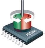
AS5045-ASST是由ams(艾迈斯半导体)生产的一款高精度磁性绝对编码器,广泛应用于需要精确角度测量和位置反馈的场合。以下是其主要应用场景:

1. 工业自动化:在工业自动化设备中,AS5045-ASST可用于电机控制、机器人关节、传送带系统等,提供精确的角度位置反馈,确保设备运行的稳定性和精度。

2. 伺服电机:该编码器可以集成到伺服电机中,用于实时监测电机转子的位置,从而实现闭环控制,提高系统的响应速度和定位精度。

3. 医疗设备:在医疗设备如手术机器人、康复器械等中,AS5045-ASST能够提供高精度的角度测量,确保设备操作的安全性和准确性。

4. 汽车电子:在汽车电子系统中,该编码器可用于转向角度传感器、油门踏板位置传感器等,帮助车辆实现更精准的驾驶控制。

5. 消费电子:在一些高端消费电子产品中,如电动工具、智能家居设备等,AS5045-ASST可以提供可靠的角度测量功能,提升用户体验。

6. 航空航天:在航空航天领域,该编码器可用于飞行控制系统的舵面位置检测、卫星天线姿态控制等,确保系统的高可靠性。

7. 精密仪器:在精密仪器如光学设备、测量仪器等中,AS5045-ASST可以提供高分辨率的角度测量,满足对精度要求极高的应用场景。

总之,AS5045-ASST凭借其高精度、小尺寸、低功耗等特点,适用于多种需要精确角度测量和位置反馈的应用场景,尤其适合对可靠性和精度有较高要求的工业和专业领域。
| 参数 | 数值 |
| 产品目录 | |
| 描述 | IC ENCODER PROG 12-BIT 16-SSOP |
| 产品分类 | 磁性传感器 - 霍尔效应,数字开关,线性,罗盘 (IC) |
| 品牌 | ams |
| 数据手册 | http://www.ams.com/eng/content/download/1288/7223 |
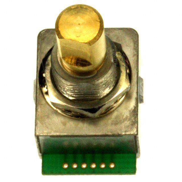
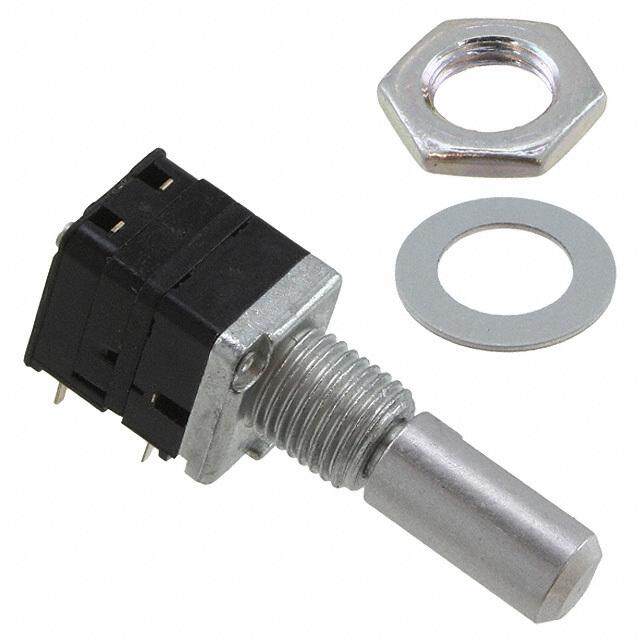
| 产品图片 |
|
| 产品型号 | AS5045-ASST |
| rohs | 无铅 / 符合限制有害物质指令(RoHS)规范要求 |
| 产品系列 | - |
| 产品目录页面 | |
| 供应商器件封装 | 16-SSOP |
| 其它名称 | AS5045-ASSTCT |
| 包装 | 剪切带 (CT) |
| 封装/外壳 | 16-SSOP(0.209",5.30mm 宽) |
| 工作温度 | -40°C ~ 125°C |
| 应用说明 | http://www.austriamicrosystems.com/eng/content/view/download/11922http://www.austriamicrosystems.com/eng/content/view/download/11921 |
| 感应范围 | 45mT ~ 75mT |
| 标准包装 | 1 |
| 特性 | 可编程 |
| 电压-电源 | 3 V ~ 3.6 V,4.5 V ~ 5.5 V |
| 电流-电源 | 21mA |
| 电流-输出(最大值) | 4mA |
| 类型 | 线性,旋转编码器 - 可编程 |
| 输出类型 | 数字式,PWM,12 位串行 |


- 商务部:美国ITC正式对集成电路等产品启动337调查
- 曝三星4nm工艺存在良率问题 高通将骁龙8 Gen1或转产台积电
- 太阳诱电将投资9.5亿元在常州建新厂生产MLCC 预计2023年完工
- 英特尔发布欧洲新工厂建设计划 深化IDM 2.0 战略
- 台积电先进制程称霸业界 有大客户加持明年业绩稳了
- 达到5530亿美元!SIA预计今年全球半导体销售额将创下新高
- 英特尔拟将自动驾驶子公司Mobileye上市 估值或超500亿美元
- 三星加码芯片和SET,合并消费电子和移动部门,撤换高东真等 CEO
- 三星电子宣布重大人事变动 还合并消费电子和移动部门
- 海关总署:前11个月进口集成电路产品价值2.52万亿元 增长14.8%

PDF Datasheet 数据手册内容提取
AS5045 12-Bit Programmable Magnetic Rotary Position Sensor General Description The AS5045 is a contactless magnetic position sensor for accurate angular measurement over a full turn of 360°. It is a system-on-chip, combining integrated Hall elements, analog front end and digital signal processing in a single device. To measure the angle, only a simple two-pole magnet, rotating over the center of the chip, is required. The magnet may be placed above or below the IC. The absolute angle measurement provides instant indication of the magnet’s angular position with a resolution of 0.0879° = 4096 positions per revolution. This digital data is available as a serial bit stream and as a PWM signal. An internal voltage regulator allows the AS5045 to operate at either 3.3 V or 5 V supplies. OrderingInformation and ContentGuide appear at end of datasheet. Key Benefits & Features The benefits and features of AS5045, 12-Bit Programmable Magnetic Rotary Position Sensor are listed below: Figure 1: Added Value of Using AS5045 Benefits Features • Highest reliability and durability in harsh • Contactless absolute angle position measurement environments • Great flexibility during assembly • User programmable zero position • Diagnostic modes for magnet detection and power supply • Operation safety loss • Lower material cost (no magnetic • Immune to external magnetic stray fields shielding needed) • Two digital 12-bit absolute outputs: • Serial interface and • Pulse width modulated (PWM) output • Failure detection mode for magnet placement monitoring and loss of power supply • “Red-Yellow-Green” indicators display placement of magnet in Z-axis ams Datasheet Page 1 [v2-01] 2017-Jul-13 DocumentFeedback
AS5045 − General Description • Serial read-out of multiple interconnected AS5045 devices using Daisy Chain mode • Tolerant to magnet misalignment and airgap variations • Wide temperature range: - 40ºC to 125ºC • Small Pb-free package: SSOP-16 (5.3mm x 6.2mm) Applications The AS5045 is ideal for industrial applications like • Robotics, • Stepper motor control, • RC servo control and • Replacement of high-end potentiometers. Block Diagram The functional blocks of this device are shown below: Figure 2: AS5045 Block Diagram VDD3V3 MagINCn MagDECn VDD5V LDO 3.3V PWM PWM Interface Sin Ang DSP Absolute DO Hall Array Cos Mag Interface CSn & (SSI) Frontend CLK Amplifier OTP Prog_DI Register AS5045 Mode Page 2 ams Datasheet DocumentFeedback [v2-01] 2017-Jul-13
AS5045 − Pin Assignment Pin Assignment Figure 3: Pin Assignment (Top View) MagINCn 1 16 VDD5V MagDECn 2 15 VDD3V3 NC 3 14 NC 5 4 NC 4 0 13 NC 5 S NC 5 A 12 PWM Mode 6 11 CSn VSS 7 10 CLK Prog_DI 8 9 DO Pin Description Figure4 shows the description of each pin of the standard SSOP16 package (Shrink Small Outline Package, 16 leads, body size: 5.3mm x 6.2mmm; see Figure3). Pins 7, 15 and 16 supply pins, pins 3, 4, 5, 6, 13 and 14 are for internal use and must not be connected. Pins 1 and 2 MagINCn and MagDECn are the magnetic field change indicators (magnetic field strength increase or decrease through variation of the distance between the magnet and the device). These outputs can be used to detect the valid magnetic field range. Furthermore those indicators can also be used for contact-less push-button functionality. Pin 6 Mode allows switching between filtered (slow) and unfiltered (fast mode). This pin must be tied to VSS or VDD5V, and must not be switched after power up. See Mode Input Pin. Pin 8 Prog is used to program the zero-position into the OTP. See Zero Position Programming. This pin is also used as digital input to shift serial data through the device in Daisy Chain configuration. See Daisy Chain Mode. Pin 11 Chip Select (CSn; active low) selects a device within a network of AS5045 magnetic position sensors and initiates serial data transfer. A logic high at CSn puts the data output pin (DO) to tri-state and terminates serial data transfer. This pin is also used for alignment mode and programming mode (see Figure 27). ams Datasheet Page 3 [v2-01] 2017-Jul-13 DocumentFeedback
AS5045 − Pin Assignment Pin 12 PWM allows a single-wire output of the 10-bit absolute position value. The value is encoded into a pulse width modulated signal with 1μs pulse width per step (1μs to 4096μs over a full turn). By using an external low pass filter, the digital PWM signal is converted into an analog voltage, making a direct replacement of potentiometers possible. Figure 4: Pin Description Pin Pin Name Pin Type Description Number Magnet Field Magnitude INCrease; active low, indicates 1 MagINCn a distance reduction between the magnet and the device surface (see Figure16). Digital output open drain Magnet Field Magnitude DECrease; active low, 2 MagDECn indicates a distance increase between the device and the magnet see Figure16). 3 NC - 4 NC - Must be left unconnected 5 NC - Select between slow (low, VSS) and fast (high, VDD5V) 6 Mode - mode. Internal pull-down resistor. Must be hard-wired on the PCB in application. 7 VSS Supply pin Negative Supply Voltage (GND) OTP Programming Input and Data Input for Daisy Chain Digital input 8 Prog_DI mode. Internal pull-down resistor (~74kΩ). Connect to pull-down VSS if not used Digital output / 9 DO Data Output of Synchronous Serial Interface tri-state Digital input, Clock Input of Synchronous Serial Interface; 10 CLK Schmitt-Trigger input Schmitt-Trigger input Digital input pull-up, Chip Select, active low; Schmitt-Trigger input, internal 11 CSn Schmitt-Trigger input pull-up resistor (~50kΩ) Pulse Width Modulation of approx. 244Hz; 1μs/step 12 PWM Digital output (optional 122Hz; 2μs/step) 13 NC - Must be left unconnected 14 NC - 3V-Regulator Output, internally regulated from VDD5V. 15 VDD3V3 Connect to VDD5V for 3V supply voltage. Do not load Supply pin externally. 16 VDD5V Positive Supply Voltage, 3.0 to 5.5 V Page 4 ams Datasheet DocumentFeedback [v2-01] 2017-Jul-13
AS5045 − Absolute Maximum Ratings Absolute Maximum Ratings Stresses beyond those listed in Absolute Maximum Ratings may cause permanent damage to the device. These are stress ratings only, and functional operation of the device at these or any other conditions beyond those indicated in Electrical Characteristics is not implied. Exposure to absolute maximum rating conditions for extended periods may affect device reliability. Figure 5: Absolute Maximum Ratings Parameter Min Max Units Comments Electrical Parameters DC supply voltage at pin VDD5V -0.3 7 V DC supply voltage at pin 5 V VDD3V3 VDD5V Input pin voltage -0.3 V Except VDD3V3 +0.3 Input current (latchup immunity) -100 100 mA EIA/JESD78 Class II Level A Electrostatic Discharge Electrostatic discharge ± 2 kV JESD22-A114E Temperature Ranges and Storage Conditions Storage temperature -55 150 ºC Min -67ºF; Max 302ºF The reflow peak soldering temperature (body temperature) specified is in accordance with IPC/JEDEC J-STD-020 “Moisture/Reflow Sensitivity Classification Package body temperature 260 ºC for Non-Hermetic Solid State Surface Mount Devices”. The lead finish for Pb-free leaded packages is matte tin (100% Sn). Relative humidity 5 85 % non-condensing Represents a maximum floor life time of Moisture sensitivity level (MSL) 3 168h ams Datasheet Page 5 [v2-01] 2017-Jul-13 DocumentFeedback
AS5045 − Electrical Characteristics Electrical Characteristics T = -40°C to 125°C, VDD5V = 3.0V to 3.6V (3V operation) AMB VDD5V = 4.5V to 5.5V (5V operation), unless otherwise noted. Figure 6: Electrical Characteristics Symbol Parameter Condition Min Typ Max Units Operating Conditions T Ambient temperature -40°F to 257°F -40 125 °C AMB I Supply current 16 21 mA supp Supply voltage at pin VDD5V 4.5 5.0 5.5 VDD5V 5V operation V Voltage regulator output VDD3V3 3.0 3.3 3.6 voltage at pin VDD3V3 Supply voltage at pin VDD5V 3.0 3.3 3.6 VDD5V 3.3V operation (pin VDD5V and VDD3V3 V Supply voltage at pin connected) VDD3V3 3.0 3.3 3.6 VDD3V3 DC Characteristics CMOS Schmitt-Trigger Inputs: CLK, CSn (CSn = Internal Pull-Up) 0.7 * V High level input voltage Normal operation V IH VDD5V 0.3 * V Low level input voltage V IL VDD5V V V Schmitt Trigger hysteresis 1 V Ion- Ioff I Input leakage current CLK only -1 1 μA LEAK Pull-up low level input I CSn only, VDD5V: 5.0V -30 -100 μA IL current DC Characteristics CMOS / Program Input: Prog 0.7 * V High level input voltage VDD5V V IH VDD5V Refer to programming VPROG High level input voltage During programming V conditions (Figure10) 0.3 * V Low level input voltage V IL VDD5V I High level input current VDD5V: 5.5V 30 100 μA IL Page 6 ams Datasheet DocumentFeedback [v2-01] 2017-Jul-13
AS5045 − Electrical Characteristics Symbol Parameter Condition Min Typ Max Units DC Characteristics CMOS Output Open Drain: MagINCn, MagDECn V Low level output voltage VSS+0.4 V OL VDD5V: 4.5V 4 I Output current mA O VDD5V: 3V 2 I Open drain leakage current 1 μA OZ DC Characteristics CMOS Output: PWM VDD5V- V High level output voltage V OH 0.5 V Low level output voltage VSS+0.4 V OL VDD5V: 4.5V 4 I Output current mA O VDD5V: 3V 2 DC Characteristics Tri-state CMOS Output: DO VDD5V- V High level output voltage V OH 0.5 V Low level output voltage VSS+0.4 V OL VDD5V: 4.5V 4 I Output current mA O VDD5V: 3V 2 I Tri-state leakage current 1 μA OZ ams Datasheet Page 7 [v2-01] 2017-Jul-13 DocumentFeedback
AS5045 − Electrical Characteristics Magnetic Input Specification Two-pole cylindrical diametrically magnetized source: Figure 7: Magnetic Input Specification Symbol Parameter Conditions Min Typ Max Units d Diameter Recommended magnet: 4 6 mm mag Ø 6mm x 2.5mm for t Thickness cylindrical magnets 2.5 mm mag Required vertical component of the magnetic field strength Magnetic input field B on the die’s surface, 45 75 mT pk amplitude measured along a concentric circle with a radius of 1.1mm B Magnetic offset Constant magnetic stray field ± 10 mT off Field non-linearity Including offset gradient 5 % 146 rpm @ 4096 2.44 Input frequency positions/rev.; fast mode f (rotational speed of Hz mag_abs magnet) 36.6rpm @ 4096 0.61 positions/rev.; slow mode Maximum offset between Disp Displacement radius defined device center and 0.25 mm magnet axis Eccentricity of magnet center Ecc Eccentricity 100 μm to rotational axis Page 8 ams Datasheet DocumentFeedback [v2-01] 2017-Jul-13
AS5045 − Electrical Characteristics Electrical System Specifications Figure 8: Input Specification Symbol Parameter Conditions Min Typ Max Units RES Resolution 0.088 deg 12 bit Maximum error with respect to the best line fit. Centered INL ± 0.5 opt magnet without calibration, T = 25°C Integral non-linearity AMB deg (optimum) Maximum error with respect to the best line fit. Centered INL ± 0.9 temp magnet without calibration, T = -40°C to 125°C AMB Best line fit = (Err – Err ) / 2 max min Over displacement tolerance INL Integral non-linearity with 6mm diameter magnet, ± 1.4 deg without calibration, T = -40°C to 125°C AMB Differential DNL 12-bit, No missing codes ±0.044 deg non-linearity 1 sigma, fast mode 0.06 (MODE = 1) deg TN Transition noise RMS 1 sigma, slow mode (MODE=0 0.03 or open) Power-on reset V thresholds: ON 1.37 2.2 2.9 On voltage; 300mV typ. hysteresis DC supply voltage 3.3V V (VDD3V3) Power-on reset V thresholds: Off voltage; 1.08 1.9 2.6 OFF 300mV typ. hysteresis Fast mode (Mode = 1); 20 until status bit OCF = 1 t Power-up time ms PwrUp Slow mode (Mode = 0 or open); 80 until OCF = 1 System propagation Fast mode (MODE=1) 96 delay absolute output : t μs delay delay of ADC, DSP and Slow mode (MODE=0 or open) 384 absolute interface ams Datasheet Page 9 [v2-01] 2017-Jul-13 DocumentFeedback
AS5045 − Electrical Characteristics Symbol Parameter Conditions Min Typ Max Units T = 25°C, AMB 2.48 2.61 2.74 slow mode (MODE=0 or open) Internal sampling rate f kHz S for absolute output: T = -40°C to 125°C, AMB 2.35 2.61 2.87 slow mode (MODE=0 or open) T = 25°C, fast mode AMB 9.90 10.42 10.94 (MODE = 1) Internal sampling rate f kHz S for absolute output T = -40°C to 125°C, AMB 9.38 10.42 11.46 fast mode (MODE = 1) Maximum clock frequency to CLK Read-out frequency 1 MHz read out serial data Figure 9: Integral and Differential Non-Linearity (Example) 4095 α 1 2 bit code 4095 Actual curve 2 TN Ideal curve 1 DNL+1LSB 0 INL 0.09° 2048 2048 0 0 ° 180° 360 ° α[degrees] Integral Non-Linearity (INL) is the maximum deviation between actual position and indicated position. Differential Non-Linearity (DNL) is the maximum deviation of the step length from one position to the next. Transition Noise (TN) is the repeatability of an indicated position. Page 10 ams Datasheet DocumentFeedback [v2-01] 2017-Jul-13
AS5045 − Timing Characteristics Timing Characteristics Figure 10: Timing Characteristics Symbol Parameter Conditions Min Typ Max Units Synchronous Serial Interface (SSI) Time between falling edge of Data output activated t CSn and data output 100 ns DO active (logic high) activated Time between falling edge of First data shifted to t CSn and first falling edge of 500 ns CLK FE output register CLK Rising edge of CLK shifts out T Start of data output 500 ns CLK / 2 one bit at a time Time between rising edge of t Data output valid 357 375 394 ns DO valid CLK and data output valid After the last bit DO changes t Data output tristate 100 ns DO tristate back to “tristate” CSn = high; To initiate t Pulse width of CSn read-out of next angular 500 ns CSn position Clock frequency to read out f Read-out frequency >0 1 MHz CLK serial data Pulse Width Modulation Output Signal period = 4097μs ±5% 232 244 256 at T = 25°C AMB f PWM frequency Hz PWM Signal period = 4097μs ±10% 220 244 268 at T = -40 to 125°C AMB PW Minimum pulse width Position 0d; Angle 0° 0.95 1 1.05 μs MIN Position 4095d; Angle PW Maximum pulse width 3891 4096 4301 μs MAX 359.91° ams Datasheet Page 11 [v2-01] 2017-Jul-13 DocumentFeedback
AS5045 − Timing Characteristics Symbol Parameter Conditions Min Typ Max Units Programming Conditions Time between rising edge at Programming enable t Prog pin and rising edge of 2 μs Prog enable time CSn t Write data start 2 μs Data in Write data at the rising edge t Write data valid 250 ns Data in valid of CLK PROG t Load programming data 3 μs Load PROG Rise time of V before t PROG 0 μs PrgR CLK PROG Hold time of V after t PROG 0 5 μs PrgH CLK PROG Write data – Ensure that V is stable CLK PROG 250 kHz PROG programming CLKPROG with rising edge of CLK During programming; 16 t CLK pulse width 1.8 2 2.2 μs PROG clock cycles Programmed data is Hold time of V after t PROG available after next 2 μs PROG finished programming power-on Programming voltage, Must be switched off after V 7.3 7.4 7.5 V PROG pin PROG zapping Programming voltage off Line must be discharged to V 0 1 V ProgOff level this level I Programming current During programming 130 mA PROG CLK Analog read CLK Analog Readback mode 100 kHz Aread Programmed Zener V 100 mV programmed voltage (log.1) VRef-VPROG during Analog Readback mode (see Analog Unprogrammed Zener Readback Mode) V 1 V unprogrammed voltage (log. 0) Page 12 ams Datasheet DocumentFeedback [v2-01] 2017-Jul-13
AS5045 − Detailed Description Detailed Description The AS5045 is manufactured in a CMOS standard process and uses a spinning current Hall technology for sensing the magnetic field distribution across the surface of the chip. The integrated Hall elements are placed around the center of the device and deliver a voltage representation of the magnetic field at the surface of the IC. Through Sigma-Delta Analog / Digital Conversion and Digital Signal-Processing (DSP) algorithms, the AS5045 provides accurate high-resolution absolute angular position information. For this purpose a Coordinate Rotation Digital Computer (CORDIC) calculates the angle and the magnitude of the Hall array signals. The DSP is also used to provide digital information at the outputs MagINCn and MagDECn that indicate movements of the used magnet towards or away from the device’s surface. A small low cost diametrically magnetized (two-pole) standard magnet provides the angular position information (see Figure 30). The AS5045 senses the orientation of the magnetic field and calculates a 12-bit binary code. This code can be accessed via a Synchronous Serial Interface (SSI). In addition, an absolute angular representation is given by a Pulse Width Modulated signal at pin 12 (PWM). This PWM signal output also allows the generation of a direct proportional analogue voltage, by using an external Low-Pass-Filter. The AS5045 is tolerant to magnet misalignment and magnetic stray fields due to differential measurement technique and Hall sensor conditioning circuitry. Figure 11: Typical Arrangement of AS5045 and Magnet ams Datasheet Page 13 [v2-01] 2017-Jul-13 DocumentFeedback
AS5045 − Detailed Description Mode Input Pin The mode input pin activates or deactivates an internal filter that is used to reduce the analog output noise. Activating the filter (Mode pin = LOW) provides a reduced output noise of 0.03° rms. At the same time, the output delay is increased to 384μs. This mode is recommended for high precision, low speed applications. Deactivating the filter (Mode pin = HIGH) reduces the output delay to 96μs and provides an output noise of 0.06° rms. This mode is recommended for higher speed applications. The MODE pin should be set at power-up. A change of the mode during operation is not allowed. Switching the Mode pin affects the following parameters. Figure 12: Slow and Fast Mode Parameters 12-Bit Absolute Angular Position Output Slow Mode Fast Mode Parameter (Mode = Low) (Mode = High, VDD5V) Sampling rate 2.61 kHz (384 μs) 10.42 kHz (96μs) Transition noise (1 sigma) ≤ 0.03° rms ≤ 0.06° rms Output delay 384μs 96μs Max. speed @ 4096 samples/rev. 38 rpm 153 rpm Max. speed @ 1024 samples/rev. 153 rpm 610 rpm Max. speed @ 256 samples/rev. 610 rpm 2441 rpm Max. speed @ 64 samples/rev. 2441 rpm 9766 rpm Page 14 ams Datasheet DocumentFeedback [v2-01] 2017-Jul-13
AS5045 − Detailed Description Synchronous Serial Interface (SSI) Figure 13: Synchronous Serial Interface with Absolute Angular Position Data CSn tCLKFE tCLKFE TCLK/2 tCSn 1 8 18 1 CLK Mag Mag Even DO D11 D10 D9 D8 D7 D6 D5 D4 D3 D2 D1 D0 OCF COF LIN D11 INC DEC PAR tDO valid tDO active Angular Position Data Status Bits tDO Tristate ams Datasheet Page 15 [v2-01] 2017-Jul-13 DocumentFeedback
AS5045 − Detailed Description If CSn changes to logic low, Data Out (DO) will change from high impedance (tri-state) to logic high and the read-out will be initiated. • After a minimum time t data is latched into the CLK FE, output shift register with the first falling edge of CLK. • Each subsequent rising CLK edge shifts out one bit of data. • The serial word contains 18 bits, the first 12 bits are the angular information D[11:0], the subsequent 6 bits contain system information, about the validity of data such as OCF, COF, LIN, Parity and Magnetic Field status (increase/decrease). • A subsequent measurement is initiated by a “high” pulse at CSn with a minimum duration of t CSn. Data Content D11:D0 – absolute angular position data (MSB is clocked out first) OCF – (Offset Compensation Finished), logic high indicates the finished Offset Compensation Algorithm COF – (CORDIC Overflow), logic high indicates an out of range error in the CORDIC part. When this bit is set, the data at D9:D0 is invalid. The absolute output maintains the last valid angular value. This alarm may be resolved by bringing the magnet within the X-Y-Z tolerance limits. LIN – (Linearity Alarm), logic high indicates that the input field generates a critical output linearity. When this bit is set, the data at D9:D0 may still be used, but can contain invalid data. This warning may be resolved by bringing the magnet within the X-Y-Z tolerance limits. Even Parity – Bit for transmission error detection of bits 1 …17 (D11 …D0, OCF, COF, LIN, MagINC, MagDEC). Placing the magnet above the chip, angular values increase in clockwise direction by default. Data D11:D0 is valid, when the status bits have the following configurations. Figure 14: Status Bit Outputs OCF COF LIN MagINC MagDEC Parity 0 0 0 1 Even checksum of bits 1 0 0 1:15 1 0 1(1) 1(1) Note(s): 1. MagInc=MagDec=1 is only recommended in YELLOW mode (see Figure16). Page 16 ams Datasheet DocumentFeedback [v2-01] 2017-Jul-13
AS5045 − Detailed Description Z-Axis Range Indication (Push Button Feature, Red/Yellow/Green Indicator) The AS5045 provides several options of detecting movement and distance of the magnet in the Z-direction. Signal indicators MagINCn and MagDECn are available both as hardware pins (pins 1 and 2) and as status bits in the serial data stream. Additionally, an OTP programming option is available with bit MagCompEn (see Figure 23) that enables additional features. In the default state, the status bits MagINC, MagDec and pins MagINCn, MagDECn have the following function. Figure 15: Magnetic Field Strength Variation Indicator Status Bits Hardware Pins OTP: Mag CompEn = 0 (default) MagINC MagDEC MagINCn MagDECn Description No distance change 0 0 Off Off Magnetic input field OK (in range, ~45mT to 75mT) Distance increase; pull-function. This state is 0 1 Off On dynamic and only active while the magnet is moving away from the chip. Distance decrease; push- function. This state is 1 0 On Off dynamic and only active while the magnet is moving towards the chip. Magnetic field is ~<45mT or >~75mT. It is still 1 1 On On possible to operate the AS5045 in this range, but not recommended ams Datasheet Page 17 [v2-01] 2017-Jul-13 DocumentFeedback
AS5045 − Detailed Description When bit MagCompEn is programmed in the OTP, the function of status bits MagINC, MagDec and pins MagINCn, MagDECn is changed to the following function. Figure 16: Magnetic Field Strength Red-Yellow-Green Indicator (OTP Option) OTP: Mag CompEn = 1 Status Bits Hardware Pins (Red-Yellow-Green Programming Option) Mag Mag Mag Mag LIN Description INC DEC INCn DECn No distance change 0 0 0 Off Off Magnetic input field OK (GREEN range, ~45mT to 75mT) YELLOW range: magnetic field is ~ 25mT to 45mT or 1 1 0 On Off ~75mT to 135mT. The AS5045 may still be operated in this range, but with slightly reduced accuracy. RED range: magnetic field is ~<25mT or >~135mT. It is 1 1 1 On On still possible to operate the AS5045 in the red range, but not recommended. All other combinations n/a n/a Not available Note(s): 1. Pin 1 (MagINCn) and pin 2 (MagDECn) are active low via open drain output and require an external pull-up resistor. If the magnetic field is in range, both outputs are turned off. The two pins may also be combined with a single pull-up resistor. In this case, the signal is high when the magnetic field is in range. It is low in all other cases (see Figure15 and Figure16). Page 18 ams Datasheet DocumentFeedback [v2-01] 2017-Jul-13
AS5045 − Detailed Description Daisy Chain Mode The Daisy Chain mode allows connection of several AS5045’s in series, while still keeping just one digital input for data transfer (see “Data IN” in Figure17). This mode is accomplished by connecting the data output (DO; pin 9) to the data input (PROG; pin 8) of the subsequent device. An RC filter must be implemented between each PROG pin of device n and DO pin of device n+1, to prevent then magnetic position sensors to enter the alignment mode, in case of ESD discharge, long cables, not conform signal levels or shape. Using the values R=100R and C=1nF allow a max. CLK frequency of 1MHz on the whole chain. The serial data of all connected devices is read from the DO pin of the first device in the chain. The length of the serial bit stream increases with every connected device, it is n * (18+1) bits: For e.g., 38 bit for two devices, 57 bit for three devices, etc. The last data bit of the first device (Parity) is followed by a dummy bit and the first data bit of the second device (D11), etc. (see Figure 18). Figure 17: Daisy Chain Hardware Configuration CSn CSn CSn CSn CLK CLK CLK CLK 100R 100R DI DO PROG DO PROG DO PROG 1nF 1nF GND GND GND MCU AS5045 AS5045 AS5045 Figure 18: Daisy Chain Mode Data Transfer CSn tCLK FE TCLK/2 1 8 18 D 1 2 3 CLK Mag Mag Even DO D11 D10 D9 D8 D7 D6 D5 D4 D3 D2 D1 D0 OCF COF LIN D11 D10 D9 INC DEC PAR tDO valid tDO active Angular Position Data Status Bits Angular Position Data 1st Device 2nd Device ams Datasheet Page 19 [v2-01] 2017-Jul-13 DocumentFeedback
AS5045 − Detailed Description Pulse Width Modulation (PWM) Output The AS5045 provides a pulse width modulated output (PWM), whose duty cycle is proportional to the measured angle: t ⋅4097 (EQ1) Position= (on )−1 t +t on off The PWM frequency is internally trimmed to an accuracy of ±5% (±10% over full temperature range). This tolerance can be cancelled by measuring the complete duty cycle as shown above. Figure 19: PWM Output Signal Angle PWMIN 0 deg (Pos 0) 1µs 4097µs PWMAX 359.91 deg (Pos 4095) 4096µs 1/fPWM Changing the PWM Frequency The PWM frequency of the AS5045 can be divided by two by setting a bit (PWMhalfEN) in the OTP register (see Programming the AS5045). With PWMhalfEN = 0, the PWM timing is as shown in Figure20. Figure 20: PWM Signal Parameters (Default mode) Symbol Parameter Typ Unit Note f PWM frequency 244 Hz Signal period: 4097μs PWM - Position 0d PW MIN pulse width 1 μs MIN - Angle 0 deg - Position 4095d PW MAX pulse width 4096 μs MAX - Angle 359.91 deg Page 20 ams Datasheet DocumentFeedback [v2-01] 2017-Jul-13
AS5045 − Detailed Description When PWMhalfEN = 1, the PWM timing is as shown in Figure21. Figure 21: PWM Signal Parameters with Half Frequency (OTP Option) Symbol Parameter Typ Unit Note f PWM frequency 122 Hz Signal period: 8194μs PWM • Position 0d PW MIN pulse width 2 μs MIN • Angle 0 deg • Position 4095d PW MAX pulse width 8192 μs MAX • Angle 359.91 deg Analog Output An analog output can be generated by averaging the PWM signal, using an external active or passive low pass filter. The analog output voltage is proportional to the angle: 0°= 0V; 360° = VDD5V. Using this method, the AS5045 can be used as direct replacement of potentiometers. Figure 22: Simple 2nd Order Passive RC Low Pass Filter R1 R2 analog out Pin12 PWM VDD C1 C2 0V Pin7 0º 360º VSS Figure22 shows an example of a simple passive low pass filter to generate the analog output. (EQ2) R1, R2 ≥ 4k7C1, C2 ≥ 1μF / 6V R1 should be greater than or equal to 4k7 to avoid loading of the PWM output. Larger values of Rx and Cx will provide better filtering and less ripple, but will also slow down the response time. ams Datasheet Page 21 [v2-01] 2017-Jul-13 DocumentFeedback
AS5045 − Detailed Description The benefits of AS5045 are as follows: • Complete system-on-chip • Flexible system solution provides absolute and PWM outputs simultaneously • Ideal for applications in harsh environments due to contactless position sensing • No calibration required Programming the AS5045 After power-on, programming the AS5045 is enabled with the rising edge of CSn and Prog = logic high. 16 bit configuration data must be serially shifted into the OTP register via the Prog pin. The first “CCW” bit is followed by the zero position data (MSB first) and the Mode setting bits. Data must be valid at the rising edge of CLK (see Figure 23). After writing the data into the OTP register it can be permanently programmed by rising the Prog pin to the programming voltage V . 16 CLK pulses (t ) must be PROG PROG applied to program the fuses (see Figure 24). To exit the programming mode, the chip must be reset by a power-on-reset. The programmed data is available after the next power-up. Note(s): During the programming process, the transitions in the programming current may cause high voltage spikes generated by the inductance of the connection cable. To avoid these spikes and possible damage to the IC, the connection wires, especially the signals Prog and VSS must be kept as short as possible. The maximum wire length between the V PROG switching transistor and pin Prog should not exceed 50mm (2 inches). To suppress eventual voltage spikes, a 10nF ceramic capacitor should be connected close to pins VPROG and VSS. This capacitor is only required for programming, it is not required for normal operation. The clock timing t must be clk selected at a proper rate to ensure that the signal Prog is stable at the rising edge of CLK (see Figure 23). Additionally, the programming supply voltage should be buffered with a 10μF capacitor mounted close to the switching transistor. This capacitor aids in providing peak currents during programming. The specified programming voltage at pin Prog is 7.3 ~ 7.5V. Refer to programming conditions in Figure10. To compensate for the voltage drop across the V switching PROG transistor, the applied programming voltage may be set slightly higher (7.5 ~ 8.0V, see Figure25). Page 22 ams Datasheet DocumentFeedback [v2-01] 2017-Jul-13
AS5045 − Detailed Description OTP Register Contents CCW: Counter Clockwise Bit ccw=0 – angular value increases in clockwise direction ccw=1 – angular value increases in counter clockwise direction Z [11:0]: Programmable Zero Position PWM dis: Disable PWM output MagCompEn: When set, activates LIN alarm both when magnetic field is too high and too low (see Figure16) PWMhalfEn: When set, PWM frequency is 122Hz or 2μs / step (when PWMhalfEN = 0, PWM frequency is 244Hz, 1μs / step) Zero Position Programming Zero position programming is an OTP option that simplifies assembly of a system, as the magnet does not need to be manually adjusted to the mechanical zero position. Once the assembly is completed, the mechanical and electrical zero positions can be matched by software. Any position within a full turn can be defined as the permanent new zero position. For zero position programming, the magnet is turned to the mechanical zero position (e.g. the “off”-position of a rotary switch) and the actual angular value is read. This value is written into the OTP register bits Z11:Z0 (see Figure 23) and programmed (see Figure 24). The zero position value may also be modified before programming, e.g. to program an electrical zero position that is 180° (half turn) from the mechanical zero position, just add 2048 to the value read at the mechanical zero position and program the new value into the OTP register. Repeated OTP Programming Although a single AS5045 OTP register bit can be programmed only once (from 0 to 1), it is possible to program other, unprogrammed bits in subsequent programming cycles. However, a bit that has already been programmed should not be programmed twice. Therefore it is recommended that bits that are already programmed are set to “0” during a programming cycle. ams Datasheet Page 23 [v2-01] 2017-Jul-13 DocumentFeedback
AS5045 − Detailed Description Non-Permanent Programming It is also possible to re-configure the AS5045 in a non-permanent way by overwriting the OTP register. This procedure is essentially a “Write Data” sequence (see Figure 23) without a subsequent OTP programming cycle. The “Write Data” sequence may be applied at any time during normal operation. This configuration remains set while the power supply voltage is above the power-on reset level (see Electrical System Specifications). See Application Note AN5000-20 for further information. Figure 23: Programming Access – Write Data (Section of Figure24) CSn tDatain Prog CCW Z11 Z10 Z9 Z8 Z7 Z6 Z5 Z4 Z3 Z2 Z1 Z0 PdWisM CMoamgp PhWalMf EN EN 1 8 16 CLKPROG tProg enable tDatain valid tclk PWM and status Zero Position bit modes Figure 24: Complete Programming Sequence Write Data Programming Mode Power Off CSn 7.5V VDD Prog Data VProgOff 0V 1 16 CLKPROG tLoad PROG tPrgH tPROG finished tPrgR tPROG Page 24 ams Datasheet DocumentFeedback [v2-01] 2017-Jul-13
AS5045 − Detailed Description Figure 25: OTP Programming Connection of AS5045 (Shown with AS5045 Demoboard) AS5045 Demoboard For programmin,g keep these6 wires IC1 B asshort as possible! S U 1 MagINCn VDD5V 16 max. length = 2 inches (5cm) connect to USB 2 MagDECn VDD3V3 15 interface on PC 3V3 3 NC NC 14 7 4 NC NC 13 6 PROG 3 VPROG 5 NC PWM12 5 DCOSN µC 2 + 6 Mode CSn 11 4 CLK 1 10µF 10n 78 PVrSoSg_DAIS5045 CDLOK190 1µF+ 22k 231 V5VDVSUDSS3VB3 GND 7Oo.VT5nSP ly…S pr e8ro.q0guVriaremGdmN foDinrg Cap only required for OTP programming Analog Readback Mode Non-volatile programming (OTP) uses on-chip zener diodes, which become permanently low resistive when subjected to a specified reverse current. The quality of the programming process depends on the amount of current that is applied during the programming process (up to 130mA). This current must be provided by an external voltage source. If this voltage source cannot provide adequate power, the zener diodes may not be programmed properly. In order to verify the quality of the programmed bit, an analog level can be read for each zener diode, giving an indication whether this particular bit was properly programmed or not. To put the AS5045 in Analog Readback Mode, a digital sequence must be applied to pins CSn, PROG and CLK as shown in Figure26. The digital level for this pin depends on the supply configuration (3.3V or 5V) (see 3.3V / 5V Operation). The second rising edge on CSn (OutpEN) changes pin PROG to a digital output and the log. high signal at pin PROG must be removed to avoid collision of outputs (grey area in Figure26). The following falling slope of CSn changes pin PROG to an analog output, providing a reference voltage V , that must be ref saved as a reference for the calculation of the subsequent programmed and unprogrammed OTP bits. Following this step, each rising slope of CLK outputs one bit of data in the reverse order as during programming ams Datasheet Page 25 [v2-01] 2017-Jul-13 DocumentFeedback
AS5045 − Detailed Description (see Figure23: Md0-MD1-Div0,Div1-Indx-Z0…Z11, ccw). If a capacitor is connected to pin PROG, it should be removed during analog readback mode to allow a fast readout rate. If the capacitor is not removed the analog voltage will take longer to stabilize due to the additional capacitance. The measured analog voltage for each bit must be subtracted from the previously measured V , and the resulting value gives ref an indication on the quality of the programmed bit: a reading of <100mV indicates a properly programmed bit and a reading of >1V indicates a properly unprogrammed bit. A reading between 100mV and 1V indicates a faulty bit, which may result in an undefined digital value, when the OTP is read at power-up. Following the 18th clock (after reading bit “ccw”), the chip must be reset by disconnecting the power supply. Figure 26: OTP Register Analog Read ProgEN OutpEN Analog Readback Data at PROG Power-on- Reset; turn off CSn supply V V ref programmed Internal PROG tdeisgti tbailt hPaWlfEMN CMoamgp PDWisM Z0 Vunprogrammed Z7 Z8 Z9 Z10 Z11 CCW EN Prog changes to Output 1 16 CLK CLK t Aread LoadProg Page 26 ams Datasheet DocumentFeedback [v2-01] 2017-Jul-13
AS5045 − Detailed Description Alignment Mode The alignment mode simplifies centering the magnet over the center of the chip to gain maximum accuracy. Alignment mode can be enabled with the falling edge of CSn while Prog = logic high (see Figure 27). The Data bits D11-D0 of the SSI change to a 12-bit displacement amplitude output. A high value indicates large X or Y displacement, but also higher absolute magnetic field strength. The magnet is properly aligned, when the difference between highest and lowest value over one full turn is at a minimum. Under normal conditions, a properly aligned magnet will result in a reading of less than 128 over a full turn. The MagINCn and MagDECn indicators will be = 1 when the alignment mode reading is < 128. At the same time, both hardware pins MagINCn (#1) and MagDECn (#2) will be pulled to VSS. A properly aligned magnet will therefore produce a MagINCn = MagDECn = 1 signal throughout a full 360° turn of the magnet. Stronger magnets or short gaps between magnet and IC may show values larger than 128. These magnets are still properly aligned as long as the difference between highest and lowest value over one full turn is at a minimum. The alignment mode can be reset to normal operation by a power-on-reset (disconnect / re-connect power supply) or by a falling edge on CSn with Prog = low. Figure 27: Enabling the Alignment Mode PROG Read-out AlignMode enable via SSI CSn 2µs 2µs min. min. Figure 28: Exiting the Alignment Mode PROG Read-out exit AlignMode via SSI CSn ams Datasheet Page 27 [v2-01] 2017-Jul-13 DocumentFeedback
AS5045 − Detailed Description 3.3V / 5V Operation The AS5045 operates either at 3.3V ±10% or at 5V ±10%. This is made possible by an internal 3.3V Low-Dropout (LDO) Voltage regulator. The internal supply voltage is always taken from the output of the LDO, meaning that the internal blocks are always operating at 3.3V. For 3.3V operation, the LDO must be bypassed by connecting VDD3V3 with VDD5V (see Figure 29). For 5V operation, the 5V supply is connected to pin VDD5V, while VDD3V3 (LDO output) must be buffered by a 2.2...10μF capacitor, which is supposed to be placed close to the supply pin (see Figure 29). The VDD3V3 output is intended for internal use only It must not be loaded with an external load (see Figure 29). Figure 29: Connections for 5V / 3.3V Supply Voltages 5V Operation 3.3V Operation 2.2... 10µF VDD3V3 VDD3V3 100n 100n VDD5V Internal VDD5V Internal LDO VDD LDO VDD DO DO + I PWM + I PWM - 4.5 - 5.5V N - 3.0 - 3.6V N T CLK T CLK E CSn E CSn R R F F A A C C E E PROG PROG VSS VSS A buffer capacitor of 100nF is recommended in both cases close to pin VDD5V. Note that pin VDD3V3 must always be buffered by a capacitor. It must not be left floating, as this may cause an instable internal 3.3V supply voltage which may lead to larger than normal jitter of the measured angle. Page 28 ams Datasheet DocumentFeedback [v2-01] 2017-Jul-13
AS5045 − Detailed Description Choosing the Proper Magnet Typically the magnet should be 6mm in diameter and ≥2.5mm in height. Magnetic materials such as rare earth AlNiCo/SmCo5 or NdFeB are recommended. The magnetic field strength perpendicular to the die surface has to be in the range of ±45mT to ±75mT (peak). The magnet’s field strength should be verified using a gauss-meter. The magnetic field B at a given distance, along a v concentric circle with a radius of 1.1mm (R1), should be in the range of ±45mT to ±75mT (see Figure 30). Figure 30: Typical Magnet (6x3mm) and Magnetic Field Distribution typ. 6mm diameter N S Magnet axis Magnet axis Verticalfield R1 component Vertical field Bv (45…75mT) component 0 360 N S R1 concentric circle; radius 1.1mm ams Datasheet Page 29 [v2-01] 2017-Jul-13 DocumentFeedback
AS5045 − Detailed Description Physical Placement of the Magnet The best linearity can be achieved by placing the center of the magnet exactly over the defined center of the chip as shown in the drawing below. Figure 31: Defined Chip Center and Magnet Displacement Radius 3.9mm 3.9mm 1 m m 5 2 3 4 2. Defined center Rd m m 5 2 43 Area of recommended maximum mag- 2. net misalignment Magnet Placement. The magnet’s center axis should be aligned within a displacement radius Rd of 0.25mm from the defined center of the IC. The magnet may be placed below or above the device. The distance should be chosen such that the magnetic field on the die surface is within the specified limits (see Figure 30). The typical distance “z” between the magnet and the package surface is 0.5mm to 1.5mm, provided the use of the recommended magnet material and dimensions (6mm x 3mm). Larger distances are possible, as long as the required magnetic field strength stays within the defined limits. However, a magnetic field outside the specified range may still produce usable results, but the out-of-range condition will be indicated by MagINCn (pin 1) and MagDECn (pin 2), see Figure4. Page 30 ams Datasheet DocumentFeedback [v2-01] 2017-Jul-13
AS5045 − Detailed Description Failure Diagnostics The AS5045 also offers several diagnostic and failure detection features: Magnetic Field Strength Diagnosis By Software: The MagINC and MagDEC status bits will both be high when the magnetic field is out of range. By Hardware: Pins #1 (MagINCn) and #2 (MagDECn) are open-drain outputs and will both be turned on (= low with external pull-up resistor) when the magnetic field is out of range. If only one of the outputs are low, the magnet is either moving towards the chip (MagINCn) or away from the chip (MagDECn). Power Supply Failure Detection By Software: If the power supply to the AS5045 is interrupted, the digital data read by the SSI will be all “0”s. Data is only valid, when bit OCF is high, hence a data stream with all “0”s is invalid. To ensure adequate low levels in the failure case, a pull-down resistor (~10kΩ) should be added between pin DO and VSS at the receiving side. By Hardware: The MagINCn and MagDECn pins are open drain outputs and require external pull-up resistors. In normal operation, these pins are high ohmic and the outputs are high (see Figure15). In a failure case, either when the magnetic field is out of range of the power supply is missing, these outputs will become low. To ensure adequate low levels in case of a broken power supply to the AS5045, the pull-up resistors (~10kΩ) from each pin must be connected to the positive supply at pin 16 (VDD5V). By Hardware, PWM Output: The PWM output is a constant stream of pulses with 1kHz repetition frequency. In case of power loss, these pulses are missing. ams Datasheet Page 31 [v2-01] 2017-Jul-13 DocumentFeedback
AS5045 − Detailed Description Angular Output Tolerances Accuracy Accuracy is defined as the error between measured angle and actual angle. It is influenced by several factors: • The non-linearity of the analog-digital converters • Internal gain and mismatch errors • Non-linearity due to misalignment of the magnet As a sum of all these errors, the accuracy with centered magnet = (Err – Err )/2 is specified as better than ±0.5 degrees @ max min 25°C (see Figure 33) Misalignment of the magnet further reduces the accuracy. Figure32 shows an example of a 3D-graph displaying non-linearity over XY-misalignment. The center of the square XY-area corresponds to a centered magnet (see dot in the center of the graph). The X- and Y- axis extends to a misalignment of ±1mm in both directions. The total misalignment area of the graph covers a square of 2x2 mm (79x79mil) with a step size of 100μm. For each misalignment step, the measurement as shown in Figure33 is repeated and the accuracy (Errmax – Errmin)/2 (e.g. 0.25°) is entered as the Z-axis in the 3D-graph. Figure 32: Example of Linearity Error over XY Misalignment Linearity Error over XY-misalignment [°] 6 5 4 3 800 2 500 200 1 0 -100 x 1000 800 600 400 200 0 0 -70-0400 y -20 -400 -600 -800 000 -1000 1 - Page 32 ams Datasheet DocumentFeedback [v2-01] 2017-Jul-13
AS5045 − Detailed Description The maximum non-linearity error on this example is better than ±1 degree (inner circle) over a misalignment radius of ~0.7mm. For volume production, the placement tolerance of the IC within the package (±0.235mm) must also be taken into account. The total nonlinearity error over process tolerances, temperature and a misalignment circle radius of 0.25mm is specified better than ±1.4 degrees. The magnet used for this measurement was a cylindrical NdFeB (Bomatec® BMN-35H) magnet with 6mm diameter and 2.5mm in height. Figure 33: Example of Linearity Error over 360° Linearity error with centered magnet [degrees] 0.5 0.4 0.3 0.2 transition noise 0.1 Errmax 0 -0.1 1 55 109 163 217 271 325 379 433 487 541 595 649 703 757 811 865 919 973 -0.2 Errmin -0.3 -0.4 -0.5 Transition Noise Transition noise is defined as the jitter in the transition between two steps. Due to the nature of the measurement principle (Hall sensors + Preamplifier + ADC), there is always a certain degree of noise involved. This transition noise voltage results in an angular transition noise at the outputs. It is specified as 0.06 degrees rms (1 sigma)1 in fast mode (pin MODE = high) and 0.03 degrees rms (1 sigma) in slow mode (pin MODE = low or open). This is the repeatability of an indicated angle at a given mechanical position. 1. Statistically, 1 sigma represents 68.27% of readings, 3 sigma represents 99.73% of readings. ams Datasheet Page 33 [v2-01] 2017-Jul-13 DocumentFeedback
AS5045 − Detailed Description The transition noise has different implications on the type of output that is used: • Absolute Output; SSI Interface: The transition noise of the absolute output can be reduced by the user by implementing averaging of readings. An averaging of 4 readings will reduce the transition noise by 6dB or 50%, e.g. from 0.03°rms to 0.015°rms (1 sigma) in slow mode. • PWM Interface: If the PWM interface is used as an analog output by adding a low pass filter, the transition noise can be reduced by lowering the cutoff frequency of the filter. If the PWM interface is used as a digital interface with a counter at the receiving side, the transition noise may again be reduced by averaging of readings. High Speed Operation Sampling Rate: The AS5045 samples the angular value at a rate of 2.61k (slow mode) or 10.42k (fast mode, selectable by pin MODE) samples per second. Consequently, the absolute outputs are updated each 384μs (96μs in fast mode). At a stationary position of the magnet, the sampling rate creates no additional error. Absolute Mode: At a sampling rate of 2.6kHz/10.4kHz, the number of samples (n) per turn for a magnet rotating at high speed can be calculated by 60 (EQ3) n = slowmode rpm⋅384μs 60 (EQ4) n = fastmode rpm⋅96μs The upper speed limit in slow mode is ~6.000rpm and ~30.000rpm in fast mode. The only restriction at high speed is that there will be fewer samples per revolution as the speed increases. Regardless of the rotational speed, the absolute angular value is always sampled at the highest resolution of 12 bit. Propagation Delays The propagation delay is the delay between the time that the sample is taken until it is converted and available as angular data. This delay is 96μs in fast mode and 384μs in slow mode. Using the SSI interface for absolute data transmission, an additional delay must be considered, caused by the asynchronous sampling (0 … 1/f ) and the time it takes the sample external control unit to read and process the angular data from the chip (maximum clock rate = 1MHz, number of bits per reading = 18). Page 34 ams Datasheet DocumentFeedback [v2-01] 2017-Jul-13
AS5045 − Detailed Description Angular Error Caused by Propagation Delay: A rotating magnet will cause an angular error caused by the output propagation delay. This error increases linearly with speed: (EQ5) e =rpm∗6* prop.delay sampling, Where: e = angular error [°] sampling rpm = rotating speed [rpm] prop.delay = propagation delay [seconds] Note(s): Since the propagation delay is known, it can be automatically compensated by the control unit processing the data from the AS5045. Internal Timing Tolerance The AS5045 does not require an external ceramic resonator or quartz. All internal clock timings for the AS5045 are generated by an on-chip RC oscillator. This oscillator is factory trimmed to ±5% accuracy at room temperature (±10% over full temperature range). This tolerance influences the ADC sampling rate and the pulse width of the PWM output. • Absolute Output; SSI Interface: A new angular value is updated every 96μs (typ.) in fast mode and every 384μs (typ.) in slow mode. • PWM Output: A new angular value is updated every 400μs (typ.). The PWM pulse timings T and T also have the on off same tolerance as the internal oscillator. If only the PWM pulse width T is used to measure the angle, the resulting on value also has this timing tolerance. However, this tolerance can be cancelled by measuring both T and T on off and calculating the angle from the duty cycle. (EQ6) t ⋅4097 Position= (on )−1 t +t on off Temperature Magnetic Temperature Coefficient: One of the major benefits of the AS5045 compared to linear Hall sensors is that it is much less sensitive to temperature. While linear Hall sensors require a compensation of the magnet’s temperature coefficients, the AS5045 automatically compensates for the varying magnetic field strength over temperature. The magnet’s temperature drift does not need to be considered, as the AS5045 operates with magnetic field strengths from ±45…±75mT. Example: An NdFeB magnet has a field strength of 75mT @ -40°C and a temperature coefficient of -0.12% per Kelvin. The temperature change is from -40° to 125° = 165K. The magnetic field change is: 165 x -0.12% = -19.8%, which corresponds to 75mT at -40°C and 60mT at 125°C. ams Datasheet Page 35 [v2-01] 2017-Jul-13 DocumentFeedback
AS5045 − Detailed Description The AS5045 can compensate for this temperature related field strength change automatically, no user adjustment is required. Accuracy over Temperature: The influence of temperature in the absolute accuracy is very low. While the accuracy is ≤ ±0.5° at room temperature, it may increase to ≤±0.9° due to increasing noise at high temperatures. Timing Tolerance over Temperature: The internal RC oscillator is factory trimmed to ±5%. Over temperature, this tolerance may increase to ±10%. Generally, the timing tolerance has no influence in the accuracy or resolution of the system, as it is used mainly for internal clock generation. The only concern to the user is the width of the PWM output pulse, which relates directly to the timing tolerance of the internal oscillator. This influence however can be cancelled by measuring the complete PWM duty cycle instead of just the PWM pulse. Differences Between AS5045 and AS5040 All parameters are similar for AS5045 and AS5040, except for the parameters given below: Figure 34: Differences Between AS5045 and AS5040 Building Block AS5045 AS5040 Resolution 12bits, 0.088°/step 10bit, 0.35°/step Read: 18bits Read: 16bits (12bits data + 6 bits status) (10bits data + 6 bits status) Data length OTP write: 18 bits OTP write: 16 bits (12bits zero position + 6 bits mode (10bits zero position + 6 bits mode selection) selection) Quadrature, step/direction and BLDC Not used motor commutation modes Incremental signals Pin 3: not used Pin 3: incremental output A_LSB_U Pin 4: not used Pin 4: incremental output B_DIR_V MagINCn, MagDECn: same feature as MagINCn, MagDECn indicate in-range or Pins 1 and 2 AS5040, additional OTP option for out-of-range magnetic field plus red-yellow-green magnetic range movement of magnet in z-axis MODE pin, switch between fast and slow Pin 6 Pin 6: Index output mode Page 36 ams Datasheet DocumentFeedback [v2-01] 2017-Jul-13
AS5045 − Detailed Description Building Block AS5045 AS5040 PWM output: frequency selectable by OTP: PWM output: Pin 12 1μs / step, 4096 steps per revolution, 1μs / step, 1024 steps per revolution, f=244Hz 2μs/ step, 4096 steps per 976Hz PWM frequency revolution, f=122Hz Selectable by MODE input pin: 2.5kHz, Sampling frequency Fixed at 10kHz @10bit resolution 10kHz 384μs (slow mode) Propagation delay 48μs 96μs (fast mode) Transition noise 0.03 degrees max. (slow mode) 0.12 degrees (rms; 1sigma) 0.06 degrees max. (fast mode) Zero position, rotational direction, PWM OTP programming Zero position, rotational direction, disable, 2 Magnetic Field indicator options incremental modes, index bit width. modes, 2 PWM frequencies ams Datasheet Page 37 [v2-01] 2017-Jul-13 DocumentFeedback
AS5045 − Package Drawings & Markings Package Drawings & Markings The device is available in 16-pin SSOP. Figure 35: Package Drawings and Dimensions Symbol Min Nom Max A 1.73 1.86 1.99 A1 0.05 0.13 0.21 A2 1.68 1.73 1.78 b 0.22 0.315 0.38 c 0.09 0.17 0.25 D 5.90 6.20 6.50 E 7.40 7.80 8.20 E1 5.00 5.30 5.60 e - 0.65 BSC - YYWWMZZ L 0.55 0.75 0.95 L1 - 1.25 REF - AS5045 @ L2 - 0.25 BSC - R 0.09 - - Q 0º 4º 8º N 16 RoHS Green Note(s): 1. Dimensions and tolerancing conform to ASME Y14.5M-1994. 2. All dimensions are in millimeters. Angles are in degrees. Figure 36: Marking: YYWWMZZ YY WW M ZZ @ Year Manufacturing week Plant identifier Assembly traceability code Sublot identifier Page 38 ams Datasheet DocumentFeedback [v2-01] 2017-Jul-13
AS5045 − Package Drawings & Markings Figure 37: Vertical Cross Section of SSOP-16 Note(s): 1. All dimensions in mm. ams Datasheet Page 39 [v2-01] 2017-Jul-13 DocumentFeedback
AS5045 − Package Drawings & Markings Recommended PCB Footprint Figure 38: PCB Footprint Recommended Footprint Data Symbol mm inch A 9.02 0.355 B 6.16 0.242 C 0.46 0.018 D 0.65 0.025 E 5.01 0.197 Page 40 ams Datasheet DocumentFeedback [v2-01] 2017-Jul-13
AS5045 − Ordering & Contact Information Ordering & Contact Information The devices are available as the standard products shown in Figure39. Figure 39: Ordering Information Ordering Code Description Package Delivery Form Delivery Quantity AS5045-ASSM 16-pin SSOP Tape & Reel 500 pcs/reel 12-Bit Programmable Magnetic Position Sensor AS5045-ASST 16-pin SSOP Tape & Reel 2000 pcs/reel Buy our products or get free samples online at: www.ams.com/ICdirect Technical Support is available at: www.ams.com/Technical-Support Provide feedback about this document at: www.ams.com/Document-Feedback For further information and requests, e-mail us at: ams_sales@ams.com For sales offices, distributors and representatives, please visit: www.ams.com/contact Headquarters ams AG Tobelbader Strasse 30 8141 Premstaetten Austria, Europe Tel: +43 (0) 3136 500 0 Website: www.ams.com ams Datasheet Page 41 [v2-01] 2017-Jul-13 DocumentFeedback
AS5045 − RoHS Compliant & ams Green Statement RoHS Compliant & ams Green RoHS: The term RoHS compliant means that ams AG products fully comply with current RoHS directives. Our semiconductor Statement products do not contain any chemicals for all 6 substance categories, including the requirement that lead not exceed 0.1% by weight in homogeneous materials. Where designed to be soldered at high temperatures, RoHS compliant products are suitable for use in specified lead-free processes. ams Green (RoHS compliant and no Sb/Br): ams Green defines that in addition to RoHS compliance, our products are free of Bromine (Br) and Antimony (Sb) based flame retardants (Br or Sb do not exceed 0.1% by weight in homogeneous material). Important Information: The information provided in this statement represents ams AG knowledge and belief as of the date that it is provided. ams AG bases its knowledge and belief on information provided by third parties, and makes no representation or warranty as to the accuracy of such information. Efforts are underway to better integrate information from third parties. ams AG has taken and continues to take reasonable steps to provide representative and accurate information but may not have conducted destructive testing or chemical analysis on incoming materials and chemicals. ams AG and ams AG suppliers consider certain information to be proprietary, and thus CAS numbers and other limited information may not be available for release. Page 42 ams Datasheet DocumentFeedback [v2-01] 2017-Jul-13
AS5045 − Copyrights & Disclaimer Copyrights & Disclaimer Copyright ams AG, Tobelbader Strasse 30, 8141 Premstaetten, Austria-Europe. Trademarks Registered. All rights reserved. The material herein may not be reproduced, adapted, merged, translated, stored, or used without the prior written consent of the copyright owner. Devices sold by ams AG are covered by the warranty and patent indemnification provisions appearing in its General Terms of Trade. ams AG makes no warranty, express, statutory, implied, or by description regarding the information set forth herein. ams AG reserves the right to change specifications and prices at any time and without notice. Therefore, prior to designing this product into a system, it is necessary to check with ams AG for current information. This product is intended for use in commercial applications. Applications requiring extended temperature range, unusual environmental requirements, or high reliability applications, such as military, medical life-support or life-sustaining equipment are specifically not recommended without additional processing by ams AG for each application. This product is provided by ams AG “AS IS” and any express or implied warranties, including, but not limited to the implied warranties of merchantability and fitness for a particular purpose are disclaimed. ams AG shall not be liable to recipient or any third party for any damages, including but not limited to personal injury, property damage, loss of profits, loss of use, interruption of business or indirect, special, incidental or consequential damages, of any kind, in connection with or arising out of the furnishing, performance or use of the technical data herein. No obligation or liability to recipient or any third party shall arise or flow out of ams AG rendering of technical or other services. ams Datasheet Page 43 [v2-01] 2017-Jul-13 DocumentFeedback
AS5045 − Document Status Document Status Document Status Product Status Definition Information in this datasheet is based on product ideas in the planning phase of development. All specifications are Product Preview Pre-Development design goals without any warranty and are subject to change without notice Information in this datasheet is based on products in the design, validation or qualification phase of development. Preliminary Datasheet Pre-Production The performance and parameters shown in this document are preliminary without any warranty and are subject to change without notice Information in this datasheet is based on products in ramp-up to full production or full production which Datasheet Production conform to specifications in accordance with the terms of ams AG standard warranty as given in the General Terms of Trade Information in this datasheet is based on products which conform to specifications in accordance with the terms of Datasheet (discontinued) Discontinued ams AG standard warranty as given in the General Terms of Trade, but these products have been superseded and should not be used for new designs Page 44 ams Datasheet DocumentFeedback [v2-01] 2017-Jul-13
AS5045 − Revision Information Revision Information Changes from 1.8 (2013-Aug-14) to current revision 2-01 (2017-Jul-13) Page 1.8 (2013-Aug-14) to 2-00 (2016-Sep-12) Content was updated to the latest ams design Added Figure 1 1 Updated Figure 39 41 2-00 (2016-Sep-12) to 2-01 (2017-Jul-13) Updated Figure 39 41 Note(s): 1. Page and figure numbers for the previous version may differ from page and figure numbers in the current revision. 2. Correction of typographical errors is not explicitly mentioned. ams Datasheet Page 45 [v2-01] 2017-Jul-13 DocumentFeedback
AS5045 − Content Guide Content Guide 1 General Description 1 Key Benefits & Features 2 Applications 2 Block Diagram 3 Pin Assignment 3 Pin Description 5 Absolute Maximum Ratings 6 Electrical Characteristics 8 Magnetic Input Specification 8 Electrical System Specifications 11 Timing Characteristics 13 Detailed Description 14 Mode Input Pin 14 Synchronous Serial Interface (SSI) 15 Data Content 16 Z-axis Range Indication (Push Button Feature, Red/Yel- low/Green Indicator) 18 Daisy Chain Mode 19 Pulse Width Modulation (PWM) Output 19 Changing the PWM Frequency 20 Analog Output 21 Programming the AS5045 22 Zero Position Programming 22 Repeated OTP Programming 23 Non-Permanent Programming 24 Analog Readback Mode 26 Alignment Mode 27 3.3V / 5V Operation 28 Choosing the Proper Magnet 29 Physical Placement of the Magnet 30 Failure Diagnostics 30 Magnetic Field Strength Diagnosis 30 Power Supply Failure Detection 31 Angular Output Tolerances 31 Accuracy 32 Transition Noise 33 High Speed Operation 33 Propagation Delays 34 Internal Timing Tolerance 34 Temperature 35 Accuracy over Temperature: 35 Differences between AS5045 and AS5040 Page 46 ams Datasheet DocumentFeedback [v2-01] 2017-Jul-13
AS5045 − Content Guide 37 Package Drawings & Markings 39 Recommended PCB Footprint 40 Ordering & Contact Information 41 RoHS Compliant & ams Green Statement 42 Copyrights & Disclaimer 43 Document Status 44 Revision Information ams Datasheet Page 47 [v2-01] 2017-Jul-13 DocumentFeedback
Mouser Electronics Authorized Distributor Click to View Pricing, Inventory, Delivery & Lifecycle Information: a ms: AS5045-ASST