ICGOO在线商城 > 集成电路(IC) > PMIC - 稳压器 - 线性 > AP2126K-ADJTRG1
 Datasheet下载
- 型号: AP2126K-ADJTRG1
- 制造商: Diodes Inc.
- 库位|库存: xxxx|xxxx
- 要求:
| 数量阶梯 | 香港交货 | 国内含税 |
| +xxxx | $xxxx | ¥xxxx |
查看当月历史价格
查看今年历史价格
AP2126K-ADJTRG1产品简介:
ICGOO电子元器件商城为您提供AP2126K-ADJTRG1由Diodes Inc.设计生产,在icgoo商城现货销售,并且可以通过原厂、代理商等渠道进行代购。 AP2126K-ADJTRG1价格参考。Diodes Inc.AP2126K-ADJTRG1封装/规格:PMIC - 稳压器 - 线性, Linear Voltage Regulator IC Positive Adjustable 1 Output 1.25 V ~ 5.5 V 300mA SOT-23-5。您可以下载AP2126K-ADJTRG1参考资料、Datasheet数据手册功能说明书,资料中有AP2126K-ADJTRG1 详细功能的应用电路图电压和使用方法及教程。
Diodes Incorporated的AP2126K-ADJTRG1是一款线性稳压器(LDO),属于电源管理集成电路(PMIC)的一部分。该器件主要用于将较高的输入电压稳定地转换为可调的较低输出电压,具备低噪声、高电源抑制比(PSRR)和快速瞬态响应等特性。

AP2126K-ADJTRG1的应用场景主要包括:

1. 便携式电子设备:如智能手机、平板电脑、数码相机等,用于为处理器、传感器或射频模块提供稳定电源。

2. 通信设备:适用于无线基站、路由器、光模块等对电源噪声敏感的通信系统中,以保证信号完整性。

3. 工业控制系统:用于工业自动化设备中的精密传感器、ADC/DAC转换器或微控制器供电。

4. 测试与测量仪器:因其低噪声特性,适合用于示波器、信号发生器等精密仪器的电源管理部分。

5. 汽车电子系统:可用于车载信息娱乐系统、驾驶辅助模块等对电源稳定性要求较高的场景。

该器件采用SOT-223封装,适合需要高效、小体积电源解决方案的设计。其可调输出电压特性使其在多种电压需求的应用中具备灵活性。
| 参数 | 数值 |
| 产品目录 | 集成电路 (IC) |
| 描述 | IC REG LDO ADJ 0.3A SOT25 |
| 产品分类 | |
| 品牌 | Diodes Incorporated |
| 数据手册 | |
| 产品图片 |
|
| 产品型号 | AP2126K-ADJTRG1 |
| rohs | 无铅 / 符合限制有害物质指令(RoHS)规范要求 |
| RoHS指令信息 | http://diodes.com/download/4349 |
| 产品系列 | - |
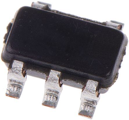
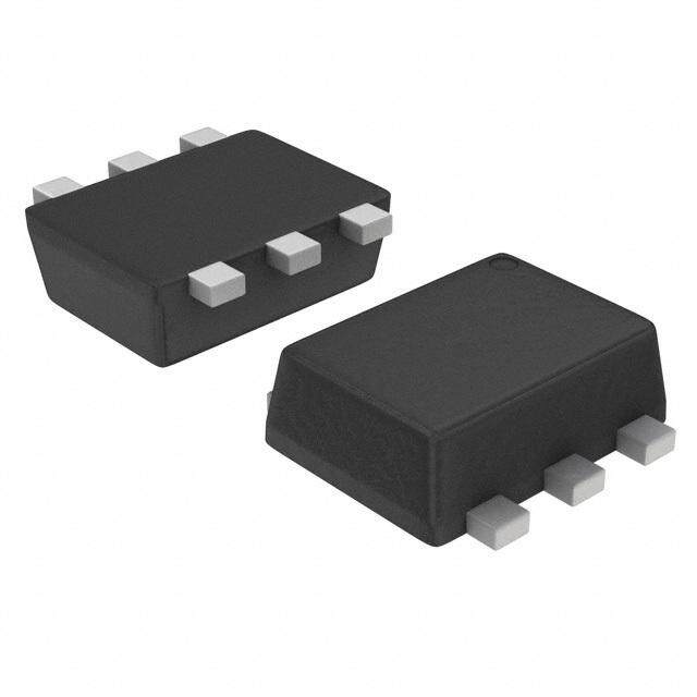
| 供应商器件封装 | SOT-23-5 |
| 其它名称 | AP2126K-ADJTRG1DIDKR |
| 包装 | Digi-Reel® |
| 安装类型 | 表面贴装 |
| 封装/外壳 | SC-74A,SOT-753 |
| 工作温度 | -40°C ~ 85°C |
| 标准包装 | 1 |
| 电压-跌落(典型值) | - |
| 电压-输入 | 3 V ~ 6 V |
| 电压-输出 | 1.25 V ~ 5.5 V |
| 电流-输出 | 300mA |
| 电流-限制(最小值) | - |
| 稳压器拓扑 | 正,可调式 |
| 稳压器数 | 1 |


- 商务部:美国ITC正式对集成电路等产品启动337调查
- 曝三星4nm工艺存在良率问题 高通将骁龙8 Gen1或转产台积电
- 太阳诱电将投资9.5亿元在常州建新厂生产MLCC 预计2023年完工
- 英特尔发布欧洲新工厂建设计划 深化IDM 2.0 战略
- 台积电先进制程称霸业界 有大客户加持明年业绩稳了
- 达到5530亿美元!SIA预计今年全球半导体销售额将创下新高
- 英特尔拟将自动驾驶子公司Mobileye上市 估值或超500亿美元
- 三星加码芯片和SET,合并消费电子和移动部门,撤换高东真等 CEO
- 三星电子宣布重大人事变动 还合并消费电子和移动部门
- 海关总署:前11个月进口集成电路产品价值2.52万亿元 增长14.8%


PDF Datasheet 数据手册内容提取
AP2126 300mA HIGH SPEED, EXTREMELY LOW NOISE CMOS LDO REGULATOR Description Pin Assignments The AP2126 series are positive voltage regulator ICs fabricated by CMOS process. (Top View) The AP2126 series have features of low dropout voltage, low noise, high output voltage accuracy, and low current consumption which VIN 1 5 VOUT make them ideal for use in various battery-powered devices. GND 2 The AP2126 is available in 1.25V to 5.5V adjustable voltage versions. The AP2126 series are available in SOT-23-5 Package. Shutdown 3 4 ADJ Features SOT-23-5 Wide Operating Voltage: 3.0V to 6V High Output Voltage Accuracy: ±2% Applications High Ripple Rejection: 68dB@ f = 1kHz, 54dB@ f = 10kHz Low Standby Current: 0.1µA Datacom Low Dropout Voltage: 170mV@300mA for VOUT = 3.3V, Notebook Computers 140mV@ 300mA for VOUT = 5.2V Mother Board Low Quiescent Current: 60µA Typical Low Output Noise: 80µVrms@VOUT = 1.25V Short Current Limit: 50mA Over Temperature Protection Compatible with Low ESR Ceramic Capacitor: 1µF for CIN and COUT Excellent Line/Load Regulation Soft Start Time: 50µs Auto Discharge Resistance: RDS(ON) = 60Ω Totally Lead-free & Fully RoHS Compliant (Notes 1 & 2) Halogen & Antimony Free. “Green” Device (Note 3) Notes: 1. No purposely added lead. Fully EU Directive 2002/95/EC (RoHS) & 2011/65/EU (RoHS 2) compliant. 2. See http://www.diodes.com/quality/lead_free.html for more information about Diodes Incorporated’s definitions of Halogen- and Antimony-free, "Green" and Lead-free. 3. Halogen- and Antimony-free "Green” products are defined as those which contain <900ppm bromine, <900ppm chlorine (<1500ppm total Br + Cl) and <1000ppm antimony compounds. Typical Applications Circuit V V IN OUT 1 5 VIN VOUT AP2126 R1 3 4 Shutdown ADJ C OUT 1µF R2 GND C IN 1µF 2 VOUT = 1.25*(1+R1/R2) V AP2126 1 of 9 May 2017 Document number: DS39758 Rev. 2 - 2 www.diodes.com © Diodes Incorporated
AP2126 Functional Block Diagram 3 Shutdown Shutdown 1 and V IN Logic Control V REF MOS Driver 5 V OUT Current Limit And Thermal Protection 4 ADJ 2 GND Absolute Maximum Ratings (Note 4) Symbol Parameter Rating Unit VIN Input Voltage 6.5 V VCE Shutdown Input Voltage -0.3 to VIN +0.3 V IOUT Output Current 450 mA TJ Junction Temperature +150 °C TSTG Storage Temperature Range -65 to +150 °C TLEAD Lead Temperature (Soldering, 10sec) +260 °C θJA Thermal Resistance (Junction to Ambient) 250 °C/W ESD ESD (Human Body Model) 6000 V ESD ESD (Machine Model) 250 V Note 4: Stresses greater than those listed under “Absolute Maximum Ratings” may cause permanent damage to the device. These are stress ratings only, and functional operation of the device at these or any other conditions beyond those indicated under “Recommended Operating Conditions” is not implied. Exposure to “Absolute Maximum Ratings” for extended periods may affect device reliability. AP2126 2 of 9 May 2017 Document number: DS39758 Rev. 2 - 2 www.diodes.com © Diodes Incorporated
AP2126 Recommended Operating Conditions Symbol Parameter Min Max Unit VIN Input Voltage 3.0 6 V TA Operating Ambient Temperature Range -40 +85 °C Electrical Characteristics (AP2126-ADJ, VIN min = 3.0V, CIN = 1µF, COUT = 1µF, unless otherwise specified.) Symbol Parameter Conditions Min Typ Max Unit VREF Reference Voltage VIN = 3.0V, 1mA ≤IOUT ≤300mA 1.225 1.25 1.275 V VIN Input Voltage — 3.0 — 6 V IOUT(MAX) Maximum Output Current VIN = 3.0V, VOUT = 98% xVOUT 300 400 — mA VOUT Load Regulation VIN = 3.0V, 1mA ≤ IOUT ≤ 300mA — — 0.6 %/A /(IOUT*VOUT) VOUT Line Regulation VIN = 3.0V to 6V, IOUT = 30mA — — 0.06 %/V /(VIN*VOUT) IQ Quiescent Current VIN = 3.0V, IOUT = 0mA — 60 90 µA ISTD Standby Current VIN = 3.0V, VShutdown in Off Mode — 0.1 1.0 µA f = 100Hz — 68 — dB Ripple 1Vp-p PSRR Power Supply Rejection Ratio f = 1kHz — 68 — dB VIN = 3.5V f = 10kHz — 54 — dB (VOUT/VOUT) Output Voltage IOUT = 30mA, -40°C TA +85°C — ±100 — ppm/°C /T Temperature Coefficient ISHORT Short Current Limit VOUT = 0V — 50 — mA tUP Soft Start Time — — 50 — µs TA = +25°C, 10Hz ≤ f ≤ 100kHz, VNOISE RMS Output Noise — 80 — µVrms VOUT = 1.25V Shutdown "High" Voltage Shutdown Input Voltage "High" — 1.5 — 6 V Shutdown "Low" Voltage Shutdown Input Voltage "Low" — 0 — 0.4 V Shutdown Input Voltage "Low" — VOUT Discharge MOSFET RDS(ON) — 60 — Ω Shutdown Pull Down Resistance — — — 3 — MΩ — Thermal Shutdown — — +165 — °C — Thermal Shutdown Hysteresis — — +30 — °C JC Thermal Resistance SOT-23-5 — 150 — °C/W AP2126 3 of 9 May 2017 Document number: DS39758 Rev. 2 - 2 www.diodes.com © Diodes Incorporated
AP2126 Performance Characteristics Output Voltage vs. Output Current Output Voltage vs. Output Current 3.5 3.5 3.0 3.0 V) 2.5 V) 2.5 e ( e ( ag 2.0 ag 2.0 Volt Volt ut 1.5 ut 1.5 p p Out 1.0 TTC==-+4205ooCC Out 1.0 VVIN==34..83VV C IN T=+85oC V =6V 0.5 V =4.3CV, V =3.3V 0.5 T=+25IN0C, V =3.3V IN OUT C OUT 0.0 0.0 0.0 0.1 0.2 0.3 0.4 0.5 0.0 0.1 0.2 0.3 0.4 0.5 Output Current (A) Output Current (A) Dropout Voltage vs. Output Current Dropout Voltage vs. Case Temperature 240 0.20 220 TC=-40oC 0.18 128000 TTC==++2855ooCC 0.16 C mV) 160 VOUT=3.3V V) 0.14 Dropout Voltage ( 1116802400000 Dropout Voltage ( 0000....00116802 IIOOUUTT==1105m0mAA 40 0.04 IOUT=300mA 20 0.02 VIN=4.3V, VOUT=3.3V 0 0.00 50 100 150 200 250 300 -40 -20 0 20 40 60 80 Output Current (mA) Case Temperature (oC) Quiescent Current vs. Output Current Quiescent Current vs. Case Temperature 115 71 I =0 Quiescent Current (A) 1117889900150505050 VIN=4 .TTT3CCCV===,-++ V4280O55UoooCTCC=3.3V Quiescent Current (A) 66666674567890 VVOIOUNUT=T4=.33.V3V 70 63 65 62 -40 -20 0 20 40 60 80 100 120 0 50 100 150 200 250 300 Output Current (mA) Case Temperature (oC) AP2126 4 of 9 May 2017 Document number: DS39758 Rev. 2 - 2 www.diodes.com © Diodes Incorporated
AP2126 Performance Characteristics (Cont.) Quiescent Current vs. Input Voltage Output Voltage vs. Case Temperature 80 3.348 I =10mA 70 3.346 OUT V =4.3V 3.344 VIN =3.3V 60 OUT cent Current (A) 345000 put Voltage (V) 33333.....333333334446802 Quies 20 TC=+25oC Out 33..333302 I =0 10 VOUT=3.3V 3.328 OUT 3.326 0 0 1 2 3 4 5 6 -40 -20 0 20 40 60 80 100 120 Input Voltage (V) Case Temperature (oC) Load Transient (Conditions: C =C =1µF, V =4.4V, V =3.3V IN OUT IN OUT Output Voltage vs. Input Voltage I =10mA to 300mA) OUT 3.5 T=-40oC C T=+25oC 3.0 TC=+85oC C I =0, V =3.3V I 2.5 OUT OUT OUT V) age ( 2.0 Volt put 1.5 Out 1.0 VOUT 0.5 0.0 0.0 0.5 1.0 1.5 2.0 2.5 3.0 3.5 Input Voltage (V) Line Transient Soft Start Time (Conditions: I =30mA, C =C =1µF, (Conditions: I =0mA, C =C =1µF, OUT IN OUT OUT IN OUT V =4V to 5V, V =3.3V) V =0 to 2V, V =3.3V) IN OUT Shutdown OUT V IN V OUT V OUT V Shutdown AP2126 5 of 9 May 2017 Document number: DS39758 Rev. 2 - 2 www.diodes.com © Diodes Incorporated
AP2126 Performance Characteristics (Cont.) PSRR vs. Frequency 100 90 IOUT=10mA I =300mA 80 ripple=O1UVTpp, C =1F, V =3.3V OUT OUT 70 60 B) R (d 50 R S 40 P 30 20 10 0 100 1000 10000 100000 Frequency (Hz) Ordering Information AP2126 X - X X X Product Name Package Output Voltage Packing RoHS/Green K : SOT-23-5 ADJ : ADJ Output TR : Tape & Reel G1 : Green Package Temperature Range Part Number Marking ID Packing SOT-23-5 -40 to +85oC AP2126K-ADJTRG1 GHH 3000/Tape & Reel Marking Information (1) SOT-23-5 (Top View) : Logo XXX XXX: Marking ID (See Ordering Information) AP2126 6 of 9 May 2017 Document number: DS39758 Rev. 2 - 2 www.diodes.com © Diodes Incorporated
AP2126 Package Outline Dimensions (All dimensions in mm(inch).) (1) Package Type: SOT-23-5 2.820(0.111) 3.100(0.122) 0.100(0.004) 0.200(0.008) 2)4) 12 00 .00. 4) 8) 59) 67) 00(00( 0 1 0 0 36 1 1 0. 0. 0.0. 0. 0. 0( (0 0( 0( 0 0 0.200(0.008) 5 0 5 7 6 0 .1 1. 2. 3. 0.700(0.028) REF 0.300(0.012) 0° 0.950(0.037) 0.500(0.020) 8° TYP 1.800(0.071) 2.000(0.079) 7) 5 0.000(0.000) 0(0.0 MAX 0.150(0.006) 5 4 1. 0.900(0.035) 1.300(0.051) AP2126 7 of 9 May 2017 Document number: DS39758 Rev. 2 - 2 www.diodes.com © Diodes Incorporated
AP2126 Suggested Pad Layout (1) Package Type: SOT-23-5 E2 G Z E1 Y X Z G X Y E1 E2 Dimensions (mm)/(inch) (mm)/(inch) (mm)/(inch) (mm)/(inch) (mm)/(inch) (mm)/(inch) Value 3.600/0.142 1.600/0.063 0.700/0.028 1.000/0.039 0.950/0.037 1.900/0.075 AP2126 8 of 9 May 2017 Document number: DS39758 Rev. 2 - 2 www.diodes.com © Diodes Incorporated
AP2126 IMPORTANT NOTICE DIODES INCORPORATED MAKES NO WARRANTY OF ANY KIND, EXPRESS OR IMPLIED, WITH REGARDS TO THIS DOCUMENT, INCLUDING, BUT NOT LIMITED TO, THE IMPLIED WARRANTIES OF MERCHANTABILITY AND FITNESS FOR A PARTICULAR PURPOSE (AND THEIR EQUIVALENTS UNDER THE LAWS OF ANY JURISDICTION). Diodes Incorporated and its subsidiaries reserve the right to make modifications, enhancements, improvements, corrections or other changes without further notice to this document and any product described herein. Diodes Incorporated does not assume any liability arising out of the application or use of this document or any product described herein; neither does Diodes Incorporated convey any license under its patent or trademark rights, nor the rights of others. Any Customer or user of this document or products described herein in such applications shall assume all risks of such use and will agree to hold Diodes Incorporated and all the companies whose products are represented on Diodes Incorporated website, harmless against all damages. Diodes Incorporated does not warrant or accept any liability whatsoever in respect of any products purchased through unauthorized sales channel. Should Customers purchase or use Diodes Incorporated products for any unintended or unauthorized application, Customers shall indemnify and hold Diodes Incorporated and its representatives harmless against all claims, damages, expenses, and attorney fees arising out of, directly or indirectly, any claim of personal injury or death associated with such unintended or unauthorized application. Products described herein may be covered by one or more United States, international or foreign patents pending. Product names and markings noted herein may also be covered by one or more United States, international or foreign trademarks. This document is written in English but may be translated into multiple languages for reference. Only the English version of this document is the final and determinative format released by Diodes Incorporated. LIFE SUPPORT Diodes Incorporated products are specifically not authorized for use as critical components in life support devices or systems without the express written approval of the Chief Executive Officer of Diodes Incorporated. As used herein: A. Life support devices or systems are devices or systems which: 1. are intended to implant into the body, or 2. support or sustain life and whose failure to perform when properly used in accordance with instructions for use provided in the labeling can be reasonably expected to result in significant injury to the user. B. A critical component is any component in a life support device or system whose failure to perform can be reasonably expected to cause the failure of the life support device or to affect its safety or effectiveness. Customers represent that they have all necessary expertise in the safety and regulatory ramifications of their life support devices or systems, and acknowledge and agree that they are solely responsible for all legal, regulatory and safety-related requirements concerning their products and any use of Diodes Incorporated products in such safety-critical, life support devices or systems, notwithstanding any devices- or systems-related information or support that may be provided by Diodes Incorporated. Further, Customers must fully indemnify Diodes Incorporated and its representatives against any damages arising out of the use of Diodes Incorporated products in such safety-critical, life support devices or systems. Copyright © 2017, Diodes Incorporated www.diodes.com AP2126 9 of 9 May 2017 Document number: DS39758 Rev. 2 - 2 www.diodes.com © Diodes Incorporated
Mouser Electronics Authorized Distributor Click to View Pricing, Inventory, Delivery & Lifecycle Information: D iodes Incorporated: AP2126K-ADJTRG1