ICGOO在线商城 > 集成电路(IC) > PMIC - 稳压器 - 线性 > LM2940IMP-5.0

 Datasheet下载
- 型号: LM2940IMP-5.0
- 制造商: Texas Instruments
- 库位|库存: xxxx|xxxx
- 要求:
| 数量阶梯 | 香港交货 | 国内含税 |
| +xxxx | $xxxx | ¥xxxx |
查看当月历史价格
查看今年历史价格
LM2940IMP-5.0产品简介:
ICGOO电子元器件商城为您提供LM2940IMP-5.0由Texas Instruments设计生产,在icgoo商城现货销售,并且可以通过原厂、代理商等渠道进行代购。 LM2940IMP-5.0价格参考¥9.51-¥11.88。Texas InstrumentsLM2940IMP-5.0封装/规格:PMIC - 稳压器 - 线性, Linear Voltage Regulator IC 1 Output 1A SOT-223-4。您可以下载LM2940IMP-5.0参考资料、Datasheet数据手册功能说明书,资料中有LM2940IMP-5.0 详细功能的应用电路图电压和使用方法及教程。
LM2940IMP-5.0是德州仪器(Texas Instruments)推出的一款低压差线性稳压器(LDO),输出电压为5.0V,最大输出电流可达1A。其主要应用场景包括:

1. 汽车电子系统:该器件具有宽输入电压范围和良好的负载/线路调节能力,适用于汽车电源系统,如车载音响、仪表盘模块、ECU(电子控制单元)等,能在冷启动或输入电压波动时稳定输出。

2. 工业控制设备:在PLC(可编程逻辑控制器)、传感器供电、工业自动化模块中,LM2940IMP-5.0可为微控制器、逻辑电路和低功耗IC提供稳定、低噪声的5V电源。

3. 便携式设备与电池供电系统:由于其低压差特性(典型值约0.5V),在电池电压接近输出电压时仍能正常工作,适合用于电池供电的便携设备,延长电池使用时间。

4. 消费类电子产品:可用于DVD播放器、小型家电、电源适配器后级稳压等场景,为敏感模拟电路或数字电路提供干净电源。

5. 电源管理模块:常作为多级电源架构中的后置稳压器,用于降低开关电源输出纹波,提高系统稳定性。

该器件具备过热保护、反向电压保护和短路限流功能,可靠性高,适合对电源稳定性要求较高的环境。其TO-263封装便于散热,适用于中等功率应用。总体而言,LM2940IMP-5.0广泛应用于需要稳定5V电源且输入电压变化较大的场合,尤其适合汽车与工业领域。
| 参数 | 数值 |
| 产品目录 | 集成电路 (IC) |
| 描述 | IC REG LDO 5V 1A SOT223 |
| 产品分类 | |
| 品牌 | Texas Instruments |
| 数据手册 | |
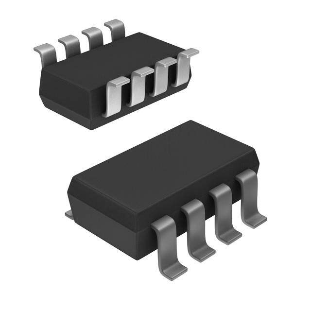
| 产品图片 |
|
| 产品型号 | LM2940IMP-5.0 |
| rohs | 含铅 / 不符合限制有害物质指令(RoHS)规范要求 |
| 产品系列 | - |
| 供应商器件封装 | SOT-223 |
| 其它名称 | LM2940IMP-5.0DKR |
| 包装 | Digi-Reel® |
| 安装类型 | 表面贴装 |
| 封装/外壳 | TO-261-4,TO-261AA |
| 工作温度 | -40°C ~ 85°C |
| 标准包装 | 1 |
| 电压-跌落(典型值) | 0.5V @ 1A |
| 电压-输入 | 6.25 V ~ 26 V |
| 电压-输出 | 5V |
| 电流-输出 | 1A |
| 电流-限制(最小值) | - |
| 稳压器拓扑 | 正,固定式 |
| 稳压器数 | 1 |


- 商务部:美国ITC正式对集成电路等产品启动337调查
- 曝三星4nm工艺存在良率问题 高通将骁龙8 Gen1或转产台积电
- 太阳诱电将投资9.5亿元在常州建新厂生产MLCC 预计2023年完工
- 英特尔发布欧洲新工厂建设计划 深化IDM 2.0 战略
- 台积电先进制程称霸业界 有大客户加持明年业绩稳了
- 达到5530亿美元!SIA预计今年全球半导体销售额将创下新高
- 英特尔拟将自动驾驶子公司Mobileye上市 估值或超500亿美元
- 三星加码芯片和SET,合并消费电子和移动部门,撤换高东真等 CEO
- 三星电子宣布重大人事变动 还合并消费电子和移动部门
- 海关总署:前11个月进口集成电路产品价值2.52万亿元 增长14.8%


PDF Datasheet 数据手册内容提取
LM2940-N, LM2940C www.ti.com SNVS769I–MARCH2000–REVISEDAPRIL2013 LM2940-N/LM2940C 1A Low Dropout Regulator CheckforSamples:LM2940-N,LM2940C FEATURES DESCRIPTION 1 • DropoutVoltageTypically0.5V@I =1A The LM2940-N/LM2940C positive voltage regulator 2 O features the ability to source 1A of output current with • OutputCurrentinExcessof1A a dropout voltage of typically 0.5V and a maximum of • OutputVoltageTrimmedBeforeAssembly 1V over the entire temperature range. Furthermore, a • ReverseBatteryProtection quiescent current reduction circuit has been included which reduces the ground current when the • InternalShortCircuitCurrentLimit differential between the input voltage and the output • MirrorImageInsertionProtection voltage exceeds approximately 3V. The quiescent • P+ProductEnhancementTested current with 1A of output current and an input-output differential of 5V is therefore only 30 mA. Higher quiescent currents only exist when the regulator is in thedropoutmode(V −V ≤ 3V). IN OUT Designed also for vehicular applications, the LM2940- N/LM2940C and all regulated circuitry are protected from reverse battery installations or 2-battery jumps. During line transients, such as load dump when the input voltage can momentarily exceed the specified maximum operating voltage, the regulator will automatically shut down to protect both the internal circuits and the load. The LM2940/LM2940C cannot be harmed by temporary mirror-image insertion. Familiar regulator features such as short circuit and thermaloverloadprotectionarealsoprovided. Typical Application *Requiredifregulatorislocatedfarfrompowersupplyfilter. **C mustbeatleast22μFtomaintainstability.Maybeincreasedwithoutboundtomaintainregulationduring OUT transients.Locateascloseaspossibletotheregulator.Thiscapacitormustberatedoverthesameoperating temperaturerangeastheregulatorandtheESRiscritical;seecurve. 1 Pleasebeawarethatanimportantnoticeconcerningavailability,standardwarranty,anduseincriticalapplicationsof TexasInstrumentssemiconductorproductsanddisclaimerstheretoappearsattheendofthisdatasheet. Alltrademarksarethepropertyoftheirrespectiveowners. 2 PRODUCTIONDATAinformationiscurrentasofpublicationdate. Copyright©2000–2013,TexasInstrumentsIncorporated Products conform to specifications per the terms of the Texas Instruments standard warranty. Production processing does not necessarilyincludetestingofallparameters.
LM2940-N, LM2940C SNVS769I–MARCH2000–REVISEDAPRIL2013 www.ti.com Connection Diagrams Figure1.TO-220(NDE)PlasticPackage Figure2.SOT-223(DCY)3-Lead FrontView FrontView SeePackageNumberNDE0003B SeePackageNumberDCY0004A Figure3.16-LeadCDIP(NFE) Figure4.16-LeadCLGA(NAC) TopView TopView SeePackageNumberNFE0016A SeePackageNumberNAC0016A Figure5.DDPAK/TO-263(KTT) Figure6.SideView TopView SeePackageNumberKTT0003B N/C 1 8 N/C GND 2 7 GND GND INPUT 3 6 VOUT N/C 4 5 VOUT Pin2andpin7arefusedtocenterDAP Pin5and6needtobetiedtogetheronPCBboard Figure7.WSON(NGN)8-Lead TopView SeePackageNumberNGN0008A Thesedeviceshavelimitedbuilt-inESDprotection.Theleadsshouldbeshortedtogetherorthedeviceplacedinconductivefoam duringstorageorhandlingtopreventelectrostaticdamagetotheMOSgates. 2 SubmitDocumentationFeedback Copyright©2000–2013,TexasInstrumentsIncorporated ProductFolderLinks:LM2940-N LM2940C
LM2940-N, LM2940C www.ti.com SNVS769I–MARCH2000–REVISEDAPRIL2013 Absolute Maximum Ratings (1)(2) LM2940-NKTT,NFE,NAC,NDE,DCY≤100ms 60V LM2940CKTT,NDE≤1ms 45V InternalPowerDissipation(3) InternallyLimited MaximumJunctionTemperature 150°C StorageTemperatureRange −65°C≤T ≤+150°C J TO-220(NDE),Wave 260°C,10s DDPAK/TO-263(KTT) 235°C,30s SolderingTemperature (4) SOT-223(DCY) 260°C,30s WSON-8(NGN) 235°C,30s ESDSusceptibility (5) 2kV (1) AbsoluteMaximumRatingsarelimitsbeyondwhichdamagetothedevicemayoccur.OperatingConditionsareconditionsunderwhich thedevicefunctionsbutthespecificationsmightnotbeensured.ForensuredspecificationsandtestconditionsseetheElectrical Characteristics. (2) IfMilitary/Aerospacespecifieddevicesarerequired,pleasecontacttheTexasInstrumentsSalesOffice/Distributorsforavailabilityand specifications. (3) Themaximumallowablepowerdissipationisafunctionofthemaximumjunctiontemperature,T,thejunction-to-ambientthermal J resistance,θ ,andtheambienttemperature,T .Exceedingthemaximumallowablepowerdissipationwillcauseexcessivedie JA A temperature,andtheregulatorwillgointothermalshutdown.Thevalueofθ (fordevicesinstillairwithnoheatsink)is60°C/Wforthe JA TO-220package,80°C/WfortheDDPAK/TO-263package,and174°C/WfortheSOT-223package.Theeffectivevalueofθ canbe JA reducedbyusingaheatsink(seeApplicationHintsforspecificinformationonheatsinking).Thevalueofθ fortheWSONpackageis JA specificallydependentonPCBtracearea,tracematerial,andthenumberoflayersandthermalvias.Forimprovedthermalresistance andpowerdissipationfortheWSONpackage,refertoApplicationNoteAN-1187(SNOA401).Itisrecommendedthat6viasbeplaced underthecenterpadtoimprovethermalperformance. (4) RefertoJEDECJ-STD-020Cforsurfacemountdevice(SMD)packagereflowprofilesandconditions.Unlessotherwisestated,the temperatureandtimeareforSn-Pb(STD)only. (5) ESDratingisbasedonthehumanbodymodel,100pFdischargedthrough1.5kΩ. Operating Conditions (1) InputVoltage 26V LM2940-NNDE,LM2940-NKTT −40°C≤T ≤125°C J LM2940CNDE,LM2940CKTT 0°C≤T ≤125°C J TemperatureRange LM2940-NDCY −40°C≤T ≤85°C A LM2940-NNFE,LM2940-NNAC −55°C≤T ≤125°C J LM2940-NNGN −40°C≤T ≤125°C J (1) AbsoluteMaximumRatingsarelimitsbeyondwhichdamagetothedevicemayoccur.OperatingConditionsareconditionsunderwhich thedevicefunctionsbutthespecificationsmightnotbeensured.ForensuredspecificationsandtestconditionsseetheElectrical Characteristics. Copyright©2000–2013,TexasInstrumentsIncorporated SubmitDocumentationFeedback 3 ProductFolderLinks:LM2940-N LM2940C
LM2940-N, LM2940C SNVS769I–MARCH2000–REVISEDAPRIL2013 www.ti.com Electrical Characteristics V =V +5V,I =1A,C =22μF,unlessotherwisespecified.Boldfacelimitsapplyovertheentireoperating IN O O O temperaturerangeoftheindicateddevice.AllotherspecificationsapplyforT =T =25°C. A J OutputVoltage(V ) 5V 8V O Parameter Conditions Typ LM2940-N LM2940- Typ LM2940-N LM2940- Units Limit(1) N/883 Limit(1) N/883 Limit(2) Limit(2) OutputVoltage 5mA≤I ≤1A 6.25V≤V ≤26V 9.4V≤V ≤26V O IN IN 5.00 4.85/4.75 4.85/4.75 8.00 7.76/7.60 7.76/7.60 V MIN 5.15/5.25 5.15/5.25 8.24/8.40 8.24/8.40 V MAX LineRegulation V +2V≤V ≤26V, O IN 20 50 40/50 20 80 50/80 mV I =5mA MAX O LoadRegulation 50mA≤I ≤1A O LM2940-N,LM2940-N/883 35 50/80 50/100 55 80/130 80/130 mV MAX LM2940C 35 50 55 80 OutputImpedance 100mADCand 20mArms, 35 1000/1000 55 1000/1000 mΩ f =120Hz O QuiescentCurrent V +2V≤V ≤26V, O IN I =5mA O LM2940-N,LM2940-N/883 10 15/20 15/20 10 15/20 15/20 mA MAX LM2940C 10 15 V =V +5V, 30 45/60 50/60 30 45/60 50/60 mA IN O MAX I =1A O OutputNoiseVoltage 10Hz−100kHz, 150 700/700 240 1000/1000 μV rms I =5mA O RippleRejection f =120Hz,1V , O rms I =100mA O LM2940-N 72 60/54 66 54/48 dB MIN LM2940C 72 60 66 54 f =1kHz,1V , 60/50 54/48 dB O rms MIN I =5mA O LongTermStability 20 32 mV/ 1000Hr DropoutVoltage I =1A 0.5 0.8/1.0 0.7/1.0 0.5 0.8/1.0 0.7/1.0 V O MAX I =100mA 110 150/200 150/200 110 150/200 150/200 mV O MAX ShortCircuit See (3) 1.9 1.6 1.5/1.3 1.9 1.6 1.6/1.3 A Current MIN MaximumLine R =100Ω O Transient LM2940-N,T≤100ms 75 60/60 75 60/60 V MIN LM2940-N/883,T≤20ms 40/40 40/40 LM2940C,T≤1ms 55 45 55 45 ReversePolarity R =100Ω O DCInputVoltage LM2940-N,LM2940-N/883 −30 −15/−15 −15/−15 −30 −15/−15 −15/−15 V MIN LM2940C −30 −15 −30 −15 (1) AlllimitsarespecifiedatT =T =25°Conly(standardtypeface)orovertheentireoperatingtemperaturerangeoftheindicateddevice A J (boldfacetype).AlllimitsatT =T =25°Care100%productiontested.Alllimitsattemperatureextremesarespecifiedviacorrelation A J usingstandardStatisticalQualityControlmethods. (2) AlllimitsarespecifiedatT =T =25°Conly(standardtypeface)orovertheentireoperatingtemperaturerangeoftheindicateddevice A J (boldfacetype).Alllimitsare100%productiontestedandareusedtocalculateOutgoingQualityLevels. (3) Outputcurrentwilldecreasewithincreasingtemperaturebutwillnotdropbelow1Aatthemaximumspecifiedtemperature. 4 SubmitDocumentationFeedback Copyright©2000–2013,TexasInstrumentsIncorporated ProductFolderLinks:LM2940-N LM2940C
LM2940-N, LM2940C www.ti.com SNVS769I–MARCH2000–REVISEDAPRIL2013 Electrical Characteristics (continued) V =V +5V,I =1A,C =22μF,unlessotherwisespecified.Boldfacelimitsapplyovertheentireoperating IN O O O temperaturerangeoftheindicateddevice.AllotherspecificationsapplyforT =T =25°C. A J OutputVoltage(V ) 5V 8V O Parameter Conditions Typ LM2940-N LM2940- Typ LM2940-N LM2940- Units Limit(1) N/883 Limit(1) N/883 Limit(2) Limit(2) ReversePolarity R =100Ω O TransientInput LM2940-N,T≤100ms −75 −50/−50 −75 −50/−50 V Voltage MIN LM2940-N/883,T≤20ms −45/−45 −45/−45 LM2940C,T≤1ms −55 −45/−45 Electrical Characteristics V =V +5V,I =1A,C =22μF,unlessotherwisespecified.Boldfacelimitsapplyovertheentireoperating IN O O O temperaturerangeoftheindicateddevice.AllotherspecificationsapplyforT =T =25°C. A J OutputVoltage(V ) 9V 10V O LM2940-N LM2940-N Units Parameter Conditions Typ Limit Typ Limit (1) (1) OutputVoltage 10.5V≤V ≤26V 11.5V≤V ≤26V IN IN 5mA≤I ≤1A 9.00 8.73/8.55 10.00 9.70/9.50 V O MIN 9.27/9.45 10.30/10.50 V MAX LineRegulation V +2V≤V ≤26V, 20 90 20 100 mV O IN MAX I =5mA O LoadRegulation 50mA≤I ≤1A O LM2940-N 60 90/150 65 100/165 mV MAX LM2940C 60 90 OutputImpedance 100mADCand 20mArms, 60 65 mΩ f =120Hz O QuiescentCurrent V +2V≤V <26V, O IN I =5mA O LM2940-N 10 15/20 10 15/20 mA MAX LM2940C 10 15 V =V +5V,I =1A 30 45/60 30 45/60 mA IN O O MAX OutputNoiseVoltage 10Hz−100kHz, 270 300 μV rms I =5mA O RippleRejection f =120Hz,1V , O rms I =100mA O LM2940-N 64 52/46 63 51/45 dB MIN LM2940C 64 52 LongTerm 34 36 mV/ Stability 1000Hr DropoutVoltage I =1A 0.5 0.8/1.0 0.5 0.8/1.0 V O MAX I =100mA 110 150/200 110 150/200 mV O MAX ShortCircuitCurrent See (2) 1.9 1.6 1.9 1.6 A MIN (1) AlllimitsarespecifiedatT =T =25°Conly(standardtypeface)orovertheentireoperatingtemperaturerangeoftheindicateddevice A J (boldfacetype).AlllimitsatT =T =25°Care100%productiontested.Alllimitsattemperatureextremesarespecifiedviacorrelation A J usingstandardStatisticalQualityControlmethods. (2) Outputcurrentwilldecreasewithincreasingtemperaturebutwillnotdropbelow1Aatthemaximumspecifiedtemperature. Copyright©2000–2013,TexasInstrumentsIncorporated SubmitDocumentationFeedback 5 ProductFolderLinks:LM2940-N LM2940C
LM2940-N, LM2940C SNVS769I–MARCH2000–REVISEDAPRIL2013 www.ti.com Electrical Characteristics (continued) V =V +5V,I =1A,C =22μF,unlessotherwisespecified.Boldfacelimitsapplyovertheentireoperating IN O O O temperaturerangeoftheindicateddevice.AllotherspecificationsapplyforT =T =25°C. A J OutputVoltage(V ) 9V 10V O LM2940-N LM2940-N Units Parameter Conditions Typ Limit Typ Limit (1) (1) MaximumLineTransient R =100Ω O T≤100ms LM2940-N 75 60/60 75 60/60 V MIN LM2940C 55 45 ReversePolarity R =100Ω O DCInputVoltage LM2940-N −30 −15/−15 −30 −15/−15 V MIN LM2940C −30 −15 ReversePolarity R =100Ω O TransientInputVoltage T≤100ms LM2940-N −75 −50/−50 −75 −50/−50 V MIN LM2940C −55 −45/−45 Electrical Characteristics V =V +5V,I =1A,C =22μF,unlessotherwisespecified.Boldfacelimitsapplyovertheentireoperating IN O O O temperaturerangeoftheindicateddevice.AllotherspecificationsapplyforT =T =25°C. A J OutputVoltage(V ) 12V 15V O Parameter Conditions Typ LM2940-N LM2940- Typ LM2940-N LM2940- Units Limit (1) N/833 Limit (1) N/833 Limit (2) Limit (2) OutputVoltage 13.6V≤V ≤26V 16.75V≤V ≤26V IN IN 5mA≤I ≤1A 12.0 11.64/11.40 11.64/11.40 15.0 14.55/14.25 14.55/14.25 V O MIN 0 0 12.36/12.60 12.36/12.60 15.45/15.75 15.45/15.75 V MAX LineRegulation V +2V≤V ≤26V, 20 120 75/120 20 150 95/150 mV O IN MAX I =5mA O LoadRegulation 50mA≤I ≤1A O LM2940-N,LM2940-N/883 55 120/200 120/190 150/240 mV MAX LM2940C 55 120 70 150 OutputImpedance 100mADCand 20mArms, 80 1000/1000 100 1000/1000 mΩ f =120Hz O Quiescent V +2V≤V ≤26V, O IN Current I =5mA O LM2940-N,LM2940-N/883 10 15/20 15/20 15/20 mA MAX LM2940C 10 15 10 15 V =V +5V,I =1A 30 45/60 50/60 30 45/60 50/60 mA IN O O MAX OutputNoise 10Hz−100kHz, 360 1000/1000 450 1000/1000 μV rms Voltage I =5mA O (1) AlllimitsarespecifiedatT =T =25°Conly(standardtypeface)orovertheentireoperatingtemperaturerangeoftheindicateddevice A J (boldfacetype).AlllimitsatT =T =25°Care100%productiontested.Alllimitsattemperatureextremesarespecifiedviacorrelation A J usingstandardStatisticalQualityControlmethods. (2) AlllimitsarespecifiedatT =T =25°Conly(standardtypeface)orovertheentireoperatingtemperaturerangeoftheindicateddevice A J (boldfacetype).Alllimitsare100%productiontestedandareusedtocalculateOutgoingQualityLevels. 6 SubmitDocumentationFeedback Copyright©2000–2013,TexasInstrumentsIncorporated ProductFolderLinks:LM2940-N LM2940C
LM2940-N, LM2940C www.ti.com SNVS769I–MARCH2000–REVISEDAPRIL2013 Electrical Characteristics (continued) V =V +5V,I =1A,C =22μF,unlessotherwisespecified.Boldfacelimitsapplyovertheentireoperating IN O O O temperaturerangeoftheindicateddevice.AllotherspecificationsapplyforT =T =25°C. A J OutputVoltage(V ) 12V 15V O Parameter Conditions Typ LM2940-N LM2940- Typ LM2940-N LM2940- Units Limit (1) N/833 Limit (1) N/833 Limit (2) Limit (2) RippleRejection f =120Hz,1V , O rms I =100mA O LM2940-N 66 54/48 dB MIN LM2940C 66 54 64 52 f =1kHz,1V , dB O rms MIN 52/46 48/42 I =5mA O LongTermStability mV/ 48 60 1000Hr DropoutVoltage I =1A 0.5 0.8/1.0 0.7/1.0 0.5 0.8/1.0 0.7/1.0 V O MAX I =100mA 110 150/200 150/200 110 150/200 150/200 mV O MAX ShortCircuitCurrent See (3) 1.9 1.6 1.6/1.3 1.9 1.6 1.6/1.3 A MIN MaximumLine R =100Ω O Transient LM2940-N,T≤100ms 75 60/60 LM2940-N/883,T≤20ms 40/40 40/40 V MIN LM2940C,T≤1ms 55 45 55 45 ReversePolarity R =100Ω O DCInputVoltage LM2940-N,LM2940-N/883 −30 −15/−15 −15/−15 −15/−15 V MIN LM2940C −30 −15 −30 −15 ReversePolarity R =100Ω O TransientInput LM2940-N,T≤100ms −75 −50/−50 Voltage LM2940-N/883,T≤20ms −45/−45 −45/−45 V MIN LM2940C,T≤1ms −55 −45/−45 −55 −45/−45 (3) Outputcurrentwilldecreasewithincreasingtemperaturebutwillnotdropbelow1Aatthemaximumspecifiedtemperature. Thermal Performance ThermalResistance 3-LeadTO-220 4 °C/W Junction-to-Case,θ(JC) 3-LeadDDPAK/TO-263 4 3-LeadTO-220 (1) 60 ThermalResistance 3-LeadDDPAK/TO-263 (1) 80 °C/W Junction-to-Ambient,θ(JA) SOT-223(1) 174 8-LeadWSON (1) 35 (1) Themaximumallowablepowerdissipationisafunctionofthemaximumjunctiontemperature,T,thejunction-to-ambientthermal J resistance,θ ,andtheambienttemperature,T .Exceedingthemaximumallowablepowerdissipationwillcauseexcessivedie JA A temperature,andtheregulatorwillgointothermalshutdown.Thevalueofθ (fordevicesinstillairwithnoheatsink)is60°C/Wforthe JA TO-220package,80°C/WfortheDDPAK/TO-263package,and174°C/WfortheSOT-223package.Theeffectivevalueofθ canbe JA reducedbyusingaheatsink(seeApplicationHintsforspecificinformationonheatsinking).Thevalueofθ fortheWSONpackageis JA specificallydependentonPCBtracearea,tracematerial,andthenumberoflayersandthermalvias.Forimprovedthermalresistance andpowerdissipationfortheWSONpackage,refertoApplicationNoteAN-1187(SNOA401).Itisrecommendedthat6viasbeplaced underthecenterpadtoimprovethermalperformance. Copyright©2000–2013,TexasInstrumentsIncorporated SubmitDocumentationFeedback 7 ProductFolderLinks:LM2940-N LM2940C
LM2940-N, LM2940C SNVS769I–MARCH2000–REVISEDAPRIL2013 www.ti.com Typical Performance Characteristics DropoutVoltage vs. DropoutVoltage Temperature Figure8. Figure9. OutputVoltage QuiescentCurrent vs. vs. Temperature Temperature Figure10. Figure11. QuiescentCurrent QuiescentCurrent Figure12. Figure13. 8 SubmitDocumentationFeedback Copyright©2000–2013,TexasInstrumentsIncorporated ProductFolderLinks:LM2940-N LM2940C
LM2940-N, LM2940C www.ti.com SNVS769I–MARCH2000–REVISEDAPRIL2013 Typical Performance Characteristics (continued) LineTransientResponse LoadTransientResponse Figure14. Figure15. RippleRejection LowVoltageBehavior Figure16. Figure17. LowVoltageBehavior LowVoltageBehavior Figure18. Figure19. Copyright©2000–2013,TexasInstrumentsIncorporated SubmitDocumentationFeedback 9 ProductFolderLinks:LM2940-N LM2940C
LM2940-N, LM2940C SNVS769I–MARCH2000–REVISEDAPRIL2013 www.ti.com Typical Performance Characteristics (continued) LowVoltageBehavior LowVoltageBehavior Figure20. Figure21. LowVoltageBehavior OutputatVoltageExtremes Figure22. Figure23. OutputatVoltageExtremes OutputatVoltageExtremes Figure24. Figure25. 10 SubmitDocumentationFeedback Copyright©2000–2013,TexasInstrumentsIncorporated ProductFolderLinks:LM2940-N LM2940C
LM2940-N, LM2940C www.ti.com SNVS769I–MARCH2000–REVISEDAPRIL2013 Typical Performance Characteristics (continued) OutputatVoltageExtremes OutputatVoltageExtremes Figure26. Figure27. OutputatVoltageExtremes OutputCapacitorESR Figure28. Figure29. PeakOutputCurrent OutputImpedance Figure30. Figure31. Copyright©2000–2013,TexasInstrumentsIncorporated SubmitDocumentationFeedback 11 ProductFolderLinks:LM2940-N LM2940C
LM2940-N, LM2940C SNVS769I–MARCH2000–REVISEDAPRIL2013 www.ti.com Typical Performance Characteristics (continued) MaximumPowerDissipation(TO-220) MaximumPowerDissipation(SOT-223) Figure32. Figure33. MaximumPowerDissipation(DDPAK/TO-263) Figure34. 12 SubmitDocumentationFeedback Copyright©2000–2013,TexasInstrumentsIncorporated ProductFolderLinks:LM2940-N LM2940C
LM2940-N, LM2940C www.ti.com SNVS769I–MARCH2000–REVISEDAPRIL2013 Equivalent Schematic Diagram Copyright©2000–2013,TexasInstrumentsIncorporated SubmitDocumentationFeedback 13 ProductFolderLinks:LM2940-N LM2940C
LM2940-N, LM2940C SNVS769I–MARCH2000–REVISEDAPRIL2013 www.ti.com APPLICATION INFORMATION EXTERNAL CAPACITORS The output capacitor is critical to maintaining regulator stability, and must meet the required conditions for both ESR(EquivalentSeriesResistance)andminimumamountofcapacitance. MINIMUMCAPACITANCE: The minimum output capacitance required to maintain stability is 22 μF (this value may be increased without limit).Largervaluesofoutputcapacitancewillgiveimprovedtransientresponse. ESRLIMITS: The ESR of the output capacitor will cause loop instability if it is too high or too low. The acceptable range of ESR plotted versus load current is shown in the graph below. It is essential that the output capacitor meet theserequirements,oroscillationscanresult. Figure35. OutputCapacitorESRLimits Itisimportanttonotethatformostcapacitors,ESRisspecifiedonlyatroomtemperature.However,thedesigner must ensure that the ESR will stay inside the limits shown over the entire operating temperature range for the design. Foraluminumelectrolyticcapacitors,ESRwillincreasebyabout30Xasthetemperatureisreducedfrom25°Cto −40°C.Thistypeofcapacitorisnotwell-suitedforlowtemperatureoperation. Solid tantalum capacitors have a more stable ESR over temperature, but are more expensive than aluminum electrolytics. A cost-effective approach sometimes used is to parallel an aluminum electrolytic with a solid Tantalum,withthetotalcapacitancesplitabout75/25%withtheAluminumbeingthelargervalue. If two capacitors are paralleled, the effective ESR is the parallel of the two individual values. The “flatter” ESR of theTantalumwillkeeptheeffectiveESRfromrisingasquicklyatlowtemperatures. HEATSINKING Aheatsinkmayberequireddependingonthemaximumpowerdissipationandmaximumambienttemperatureof the application. Under all possible operating conditions, the junction temperature must be within the range specifiedunderAbsoluteMaximumRatings. Todetermineifaheatsinkisrequired,thepowerdissipatedbytheregulator,P ,mustbecalculated. D The figure below shows the voltages and currents which are present in the circuit, as well as the formula for calculatingthepowerdissipatedintheregulator: 14 SubmitDocumentationFeedback Copyright©2000–2013,TexasInstrumentsIncorporated ProductFolderLinks:LM2940-N LM2940C
LM2940-N, LM2940C www.ti.com SNVS769I–MARCH2000–REVISEDAPRIL2013 I =I +I IN L G P =(V −V )I +(V )I D IN OUT L IN G Figure36. PowerDissipationDiagram The next parameter which must be calculated is the maximum allowable temperature rise, T . This is R(MAX) calculatedbyusingtheformula: T =T −T R(MAX) J(MAX) A(MAX) where • T isthemaximumallowablejunctiontemperature,whichis125°Cforcommercialgradeparts. J(MAX) • T isthemaximumambienttemperaturewhichwillbeencounteredintheapplication. (1) A(MAX) Using the calculated values for T and P , the maximum allowable value for the junction-to-ambient thermal R(MAX) D resistance,θ ,cannowbefound: (JA) θ =T /P (2) (JA) R(MAX) D NOTE If the maximum allowable value for θ is found to be ≥ 53°C/W for the TO-220 package, (JA) ≥ 80°C/W for the DDPAK/TO-263 package, or ≥ 174°C/W for the SOT-223 package, no heatsink is needed since the package alone will dissipate enough heat to satisfy these requirements. Ifthecalculatedvalueforθ fallsbelowtheselimits,aheatsinkisrequired. (JA) HEATSINKINGTO-220PACKAGEPARTS TheTO-220canbeattachedtoatypicalheatsink,orsecuredtoacopperplaneonaPCboard.Ifacopperplane istobeused,thevaluesofθ willbethesameasshowninthenextsectionfortheDDPAK/TO-263. (JA) If a manufactured heatsink is to be selected, the value of heatsink-to-ambient thermal resistance, θ , must (H−A) firstbecalculated: θ =θ −θ −θ (H−A) (JA) (C−H) (J−C) where • θ isdefinedasthethermalresistancefromthejunctiontothesurfaceofthecase.Avalueof3°C/Wcanbe (J−C) assumedforθ forthiscalculation. (J−C) • θ isdefinedasthethermalresistancebetweenthecaseandthesurfaceoftheheatsink.Thevalue (C−H) ofθ willvaryfromabout1.5°C/Wtoabout2.5°C/W(dependingonmethodofattachment,insulator,etc.).If (C−H) theexactvalueisunknown,2°C/Wshouldbeassumedforθ . (3) (C−H) When a value for θ is found using the equation shown, a heatsink must be selected that has a value that is (H−A) lessthanorequaltothisnumber. θ is specified numerically by the heatsink manufacturer in the catalog, or shown in a curve that plots (H−A) temperaturerisevspowerdissipationfortheheatsink. HEATSINKINGDDPAK/TO-263PACKAGEPARTS The DDPAK/TO-263 (KTT) package uses a copper plane on the PCB and the PCB itself as a heatsink. To optimizetheheatsinkingabilityoftheplaneandPCB,solderthetabofthepackagetotheplane. Figure 37 shows for the DDPAK/TO-263 the measured values of θ for different copper area sizes using a (JA) typicalPCBwith1ouncecopperandnosoldermaskoverthecopperareausedforheatsinking. Copyright©2000–2013,TexasInstrumentsIncorporated SubmitDocumentationFeedback 15 ProductFolderLinks:LM2940-N LM2940C
LM2940-N, LM2940C SNVS769I–MARCH2000–REVISEDAPRIL2013 www.ti.com Figure37. θ vs.Copper(1ounce)AreafortheDDPAK/TO-263Package (JA) As shown in the figure, increasing the copper area beyond 1 square inch produces very little improvement. It should also be observed that the minimum value of θ for the DDPAK/TO-263 package mounted to a PCB is (JA) 32°C/W. As a design aid, Figure 38 shows the maximum allowable power dissipation compared to ambient temperature for the DDPAK/TO-263 device. This assumes a θ of 35°C/W for 1 square inch of 1 ounce copper and a (JA) maximumjunctiontemperature(T )of125°C. J Figure38. MaximumPowerDissipationvs.T fortheDDPAK/TO-263Package A HEATSINKINGSOT-223PACKAGEPARTS The SOT-223 (DCY) packages use a copper plane on the PCB and the PCB itself as a heatsink. To optimize the heatsinkingabilityoftheplaneandPCB,solderthetabofthepackagetotheplane. Figure 39 and Figure 40 show the information for the SOT-223 package. Figure 40 assumes a θ of 74°C/W (JA) for 1 square inch of 1 ounce copper and 51°C/W for 1 square inch of 2 ounce copper, with a maximum ambient temperature(T )of85°Candamaximumjunctiontemperature(T )of125°C. A J For techniques for improving the thermal resistance and power dissipation for the SOT-223 package, please refertoApplicationNoteAN-1028(SNVA036). 16 SubmitDocumentationFeedback Copyright©2000–2013,TexasInstrumentsIncorporated ProductFolderLinks:LM2940-N LM2940C
LM2940-N, LM2940C www.ti.com SNVS769I–MARCH2000–REVISEDAPRIL2013 Figure39. θ vs.Copper(2ounce)AreafortheSOT-223Package (JA) Figure40. MaximumPowerDissipationvs.T fortheSOT-223Package A HEATSINKINGWSONPACKAGEPARTS The value of θ for the WSON package is specifically dependent on PCB trace area, trace material, and the JA number of layers and thermal vias. It is recommended that a minimum of 6 thermal vias be placed under the centerpadtoimprovethermalperformance. For techniques for improving the thermal resistance and power dissipation for the WSON package, please refer toApplicationNoteAN-1187(SNOA401). Copyright©2000–2013,TexasInstrumentsIncorporated SubmitDocumentationFeedback 17 ProductFolderLinks:LM2940-N LM2940C
LM2940-N, LM2940C SNVS769I–MARCH2000–REVISEDAPRIL2013 www.ti.com REVISION HISTORY ChangesfromRevisionH(April2013)toRevisionI Page • ChangedlayoutofNationalDataSheettoTIformat.......................................................................................................... 17 18 SubmitDocumentationFeedback Copyright©2000–2013,TexasInstrumentsIncorporated ProductFolderLinks:LM2940-N LM2940C
PACKAGE OPTION ADDENDUM www.ti.com 23-Sep-2013 PACKAGING INFORMATION Orderable Device Status Package Type Package Pins Package Eco Plan Lead/Ball Finish MSL Peak Temp Op Temp (°C) Device Marking Samples (1) Drawing Qty (2) (3) (4/5) LM2940CS-12 ACTIVE DDPAK/ KTT 3 45 TBD Call TI Call TI 0 to 125 LM2940CS TO-263 -12 P+ LM2940CS-12/NOPB ACTIVE DDPAK/ KTT 3 45 Pb-Free (RoHS CU SN Level-3-245C-168 HR 0 to 125 LM2940CS TO-263 Exempt) -12 P+ LM2940CS-15 ACTIVE DDPAK/ KTT 3 45 TBD Call TI Call TI 0 to 125 LM2940CS TO-263 -15 P+ LM2940CS-15/NOPB ACTIVE DDPAK/ KTT 3 45 Pb-Free (RoHS CU SN Level-3-245C-168 HR 0 to 125 LM2940CS TO-263 Exempt) -15 P+ LM2940CS-5.0 ACTIVE DDPAK/ KTT 3 45 TBD Call TI Call TI 0 to 125 LM2940CS TO-263 -5.0 P+ LM2940CS-5.0/NOPB ACTIVE DDPAK/ KTT 3 45 Pb-Free (RoHS CU SN Level-3-245C-168 HR 0 to 125 LM2940CS TO-263 Exempt) -5.0 P+ LM2940CS-9.0 ACTIVE DDPAK/ KTT 3 TBD Call TI Call TI 0 to 125 LM2940CS TO-263 -9.0 P+ LM2940CS-9.0/NOPB ACTIVE DDPAK/ KTT 3 45 Pb-Free (RoHS CU SN Level-3-245C-168 HR 0 to 125 LM2940CS TO-263 Exempt) -9.0 P+ LM2940CSX-12 ACTIVE DDPAK/ KTT 3 500 TBD Call TI Call TI 0 to 125 LM2940CS TO-263 -12 P+ LM2940CSX-12/NOPB ACTIVE DDPAK/ KTT 3 500 Pb-Free (RoHS CU SN Level-3-245C-168 HR 0 to 125 LM2940CS TO-263 Exempt) -12 P+ LM2940CSX-15 ACTIVE DDPAK/ KTT 3 500 TBD Call TI Call TI 0 to 125 LM2940CS TO-263 -15 P+ LM2940CSX-15/NOPB ACTIVE DDPAK/ KTT 3 500 Pb-Free (RoHS CU SN Level-3-245C-168 HR 0 to 125 LM2940CS TO-263 Exempt) -15 P+ LM2940CSX-5.0 ACTIVE DDPAK/ KTT 3 500 TBD Call TI Call TI 0 to 125 LM2940CS TO-263 -5.0 P+ LM2940CSX-5.0/NOPB ACTIVE DDPAK/ KTT 3 500 Pb-Free (RoHS CU SN Level-3-245C-168 HR 0 to 125 LM2940CS TO-263 Exempt) -5.0 P+ LM2940CSX-9.0 ACTIVE DDPAK/ KTT 3 TBD Call TI Call TI 0 to 125 LM2940CS TO-263 -9.0 P+ LM2940CSX-9.0/NOPB ACTIVE DDPAK/ KTT 3 500 Pb-Free (RoHS CU SN Level-3-245C-168 HR 0 to 125 LM2940CS TO-263 Exempt) -9.0 P+ LM2940CT-12 ACTIVE TO-220 NDE 3 45 TBD Call TI Call TI 0 to 125 LM2940CT -12 P+ Addendum-Page 1
PACKAGE OPTION ADDENDUM www.ti.com 23-Sep-2013 Orderable Device Status Package Type Package Pins Package Eco Plan Lead/Ball Finish MSL Peak Temp Op Temp (°C) Device Marking Samples (1) Drawing Qty (2) (3) (4/5) LM2940CT-12/NOPB ACTIVE TO-220 NDE 3 45 Green (RoHS CU SN Level-1-NA-UNLIM 0 to 125 LM2940CT & no Sb/Br) -12 P+ LM2940CT-15 ACTIVE TO-220 NDE 3 45 TBD Call TI Call TI 0 to 125 LM2940CT -15 P+ LM2940CT-15/NOPB ACTIVE TO-220 NDE 3 45 Green (RoHS CU SN Level-1-NA-UNLIM 0 to 125 LM2940CT & no Sb/Br) -15 P+ LM2940CT-5.0 ACTIVE TO-220 NDE 3 45 TBD Call TI Call TI 0 to 125 LM2940CT -5.0 P+ LM2940CT-5.0/LF01 ACTIVE TO-220 NDG 3 45 Pb-Free (RoHS CU SN Level-3-245C-168 HR LM2940CT Exempt) -5.0 P+ LM2940CT-5.0/NOPB ACTIVE TO-220 NDE 3 45 Green (RoHS CU SN Level-1-NA-UNLIM 0 to 125 LM2940CT & no Sb/Br) -5.0 P+ LM2940CT-9.0 ACTIVE TO-220 NDE 3 TBD Call TI Call TI 0 to 125 LM2940CT -9.0 P+ LM2940CT-9.0/NOPB ACTIVE TO-220 NDE 3 45 Green (RoHS CU SN Level-1-NA-UNLIM 0 to 125 LM2940CT & no Sb/Br) -9.0 P+ LM2940IMP-10 ACTIVE SOT-223 DCY 4 1000 TBD Call TI Call TI -40 to 85 L55B LM2940IMP-10/NOPB ACTIVE SOT-223 DCY 4 1000 Green (RoHS CU SN Level-1-260C-UNLIM -40 to 85 L55B & no Sb/Br) LM2940IMP-12 ACTIVE SOT-223 DCY 4 1000 TBD Call TI Call TI -40 to 85 L56B LM2940IMP-12/NOPB ACTIVE SOT-223 DCY 4 1000 Green (RoHS CU SN Level-1-260C-UNLIM -40 to 85 L56B & no Sb/Br) LM2940IMP-15 ACTIVE SOT-223 DCY 4 1000 TBD Call TI Call TI -40 to 85 L70B LM2940IMP-15/NOPB ACTIVE SOT-223 DCY 4 1000 Green (RoHS CU SN Level-1-260C-UNLIM -40 to 85 L70B & no Sb/Br) LM2940IMP-5.0 ACTIVE SOT-223 DCY 4 1000 TBD Call TI Call TI -40 to 85 L53B LM2940IMP-5.0/NOPB ACTIVE SOT-223 DCY 4 1000 Green (RoHS CU SN Level-1-260C-UNLIM -40 to 85 L53B & no Sb/Br) LM2940IMP-9.0 ACTIVE SOT-223 DCY 4 TBD Call TI Call TI -40 to 85 L0EB LM2940IMP-9.0/NOPB ACTIVE SOT-223 DCY 4 1000 Green (RoHS CU SN Level-1-260C-UNLIM -40 to 85 L0EB & no Sb/Br) LM2940IMPX-10 ACTIVE SOT-223 DCY 4 TBD Call TI Call TI -40 to 85 L55B Addendum-Page 2
PACKAGE OPTION ADDENDUM www.ti.com 23-Sep-2013 Orderable Device Status Package Type Package Pins Package Eco Plan Lead/Ball Finish MSL Peak Temp Op Temp (°C) Device Marking Samples (1) Drawing Qty (2) (3) (4/5) LM2940IMPX-10/NOPB ACTIVE SOT-223 DCY 4 2000 Green (RoHS CU SN Level-1-260C-UNLIM -40 to 85 L55B & no Sb/Br) LM2940IMPX-12 ACTIVE SOT-223 DCY 4 TBD Call TI Call TI -40 to 85 L56B LM2940IMPX-12/NOPB ACTIVE SOT-223 DCY 4 2000 Green (RoHS CU SN Level-1-260C-UNLIM -40 to 85 L56B & no Sb/Br) LM2940IMPX-5.0 ACTIVE SOT-223 DCY 4 2000 TBD Call TI Call TI -40 to 85 L53B LM2940IMPX-5.0/NOPB ACTIVE SOT-223 DCY 4 2000 Green (RoHS CU SN Level-1-260C-UNLIM -40 to 85 L53B & no Sb/Br) LM2940IMPX-8.0 ACTIVE SOT-223 DCY 4 TBD Call TI Call TI -40 to 85 L54B LM2940IMPX-8.0/NOPB ACTIVE SOT-223 DCY 4 2000 Green (RoHS CU SN Level-1-260C-UNLIM -40 to 85 L54B & no Sb/Br) LM2940LD-12 ACTIVE WSON NGN 8 1000 TBD Call TI Call TI -40 to 125 L00018B LM2940LD-12/NOPB ACTIVE WSON NGN 8 1000 Green (RoHS CU SN Level-3-260C-168 HR -40 to 125 L00018B & no Sb/Br) LM2940LD-5.0 ACTIVE WSON NGN 8 1000 TBD Call TI Call TI -40 to 125 L00014B LM2940LD-5.0/NOPB ACTIVE WSON NGN 8 1000 Green (RoHS CU SN Level-3-260C-168 HR -40 to 125 L00014B & no Sb/Br) LM2940S-10 ACTIVE DDPAK/ KTT 3 45 TBD Call TI Call TI -40 to 125 LM2940S TO-263 -10 P+ LM2940S-10/NOPB ACTIVE DDPAK/ KTT 3 45 Pb-Free (RoHS CU SN Level-3-245C-168 HR -40 to 125 LM2940S TO-263 Exempt) -10 P+ LM2940S-12 ACTIVE DDPAK/ KTT 3 45 TBD Call TI Call TI -40 to 125 LM2940S TO-263 -12 P+ LM2940S-12/NOPB ACTIVE DDPAK/ KTT 3 45 Pb-Free (RoHS CU SN Level-3-245C-168 HR -40 to 125 LM2940S TO-263 Exempt) -12 P+ LM2940S-5.0 ACTIVE DDPAK/ KTT 3 45 TBD Call TI Call TI -40 to 125 LM2940S TO-263 -5.0 P+ LM2940S-5.0/NOPB ACTIVE DDPAK/ KTT 3 45 Pb-Free (RoHS CU SN Level-3-245C-168 HR -40 to 125 LM2940S TO-263 Exempt) -5.0 P+ LM2940S-8.0 ACTIVE DDPAK/ KTT 3 TBD Call TI Call TI -40 to 125 LM2940S TO-263 -8.0 P+ LM2940S-8.0/NOPB ACTIVE DDPAK/ KTT 3 45 Pb-Free (RoHS CU SN Level-3-245C-168 HR -40 to 125 LM2940S TO-263 Exempt) -8.0 P+ Addendum-Page 3
PACKAGE OPTION ADDENDUM www.ti.com 23-Sep-2013 Orderable Device Status Package Type Package Pins Package Eco Plan Lead/Ball Finish MSL Peak Temp Op Temp (°C) Device Marking Samples (1) Drawing Qty (2) (3) (4/5) LM2940S-9.0 ACTIVE DDPAK/ KTT 3 TBD Call TI Call TI -40 to 125 LM2940S TO-263 -9.0 P+ LM2940S-9.0/NOPB ACTIVE DDPAK/ KTT 3 45 Pb-Free (RoHS CU SN Level-3-245C-168 HR -40 to 125 LM2940S TO-263 Exempt) -9.0 P+ LM2940SX-10 ACTIVE DDPAK/ KTT 3 500 TBD Call TI Call TI -40 to 125 LM2940S TO-263 -10 P+ LM2940SX-10/NOPB ACTIVE DDPAK/ KTT 3 500 Pb-Free (RoHS CU SN Level-3-245C-168 HR -40 to 125 LM2940S TO-263 Exempt) -10 P+ LM2940SX-12 ACTIVE DDPAK/ KTT 3 500 TBD Call TI Call TI -40 to 125 LM2940S TO-263 -12 P+ LM2940SX-12/NOPB ACTIVE DDPAK/ KTT 3 500 Pb-Free (RoHS CU SN Level-3-245C-168 HR -40 to 125 LM2940S TO-263 Exempt) -12 P+ LM2940SX-5.0 ACTIVE DDPAK/ KTT 3 500 TBD Call TI Call TI -40 to 125 LM2940S TO-263 -5.0 P+ LM2940SX-5.0/NOPB ACTIVE DDPAK/ KTT 3 500 Pb-Free (RoHS CU SN Level-3-245C-168 HR -40 to 125 LM2940S TO-263 Exempt) -5.0 P+ LM2940SX-8.0 ACTIVE DDPAK/ KTT 3 500 TBD Call TI Call TI -40 to 125 LM2940S TO-263 -8.0 P+ LM2940SX-8.0/NOPB ACTIVE DDPAK/ KTT 3 500 Pb-Free (RoHS CU SN Level-3-245C-168 HR -40 to 125 LM2940S TO-263 Exempt) -8.0 P+ LM2940SX-9.0 ACTIVE DDPAK/ KTT 3 500 TBD Call TI Call TI -40 to 125 LM2940S TO-263 -9.0 P+ LM2940SX-9.0/NOPB ACTIVE DDPAK/ KTT 3 500 Pb-Free (RoHS CU SN Level-3-245C-168 HR -40 to 125 LM2940S TO-263 Exempt) -9.0 P+ LM2940T-10.0 ACTIVE TO-220 NDE 3 45 TBD Call TI Call TI -40 to 125 LM2940T 10.0 P+ LM2940T-10.0/NOPB ACTIVE TO-220 NDE 3 45 Green (RoHS CU SN Level-1-NA-UNLIM -40 to 125 LM2940T & no Sb/Br) 10.0 P+ LM2940T-12.0 ACTIVE TO-220 NDE 3 45 TBD Call TI Call TI -40 to 125 LM2940T 12.0 P+ LM2940T-12.0/NOPB ACTIVE TO-220 NDE 3 45 Green (RoHS CU SN Level-1-NA-UNLIM -40 to 125 LM2940T & no Sb/Br) 12.0 P+ LM2940T-5.0 ACTIVE TO-220 NDE 3 45 TBD Call TI Call TI -40 to 125 LM2940T -5.0 P+ LM2940T-5.0/LF08 ACTIVE TO-220 NEB 3 45 Green (RoHS CU SN Level-3-245C-168 HR LM2940T & no Sb/Br) -5.0 P+ Addendum-Page 4
PACKAGE OPTION ADDENDUM www.ti.com 23-Sep-2013 Orderable Device Status Package Type Package Pins Package Eco Plan Lead/Ball Finish MSL Peak Temp Op Temp (°C) Device Marking Samples (1) Drawing Qty (2) (3) (4/5) LM2940T-5.0/NOPB ACTIVE TO-220 NDE 3 45 Green (RoHS CU SN Level-1-NA-UNLIM -40 to 125 LM2940T & no Sb/Br) -5.0 P+ LM2940T-8.0 ACTIVE TO-220 NDE 3 45 TBD Call TI Call TI -40 to 125 LM2940T -8.0 P+ LM2940T-8.0/NOPB ACTIVE TO-220 NDE 3 45 Green (RoHS CU SN Level-1-NA-UNLIM -40 to 125 LM2940T & no Sb/Br) -8.0 P+ LM2940T-9.0 ACTIVE TO-220 NDE 3 45 TBD Call TI Call TI -40 to 125 LM2940T -9.0 P+ LM2940T-9.0/NOPB ACTIVE TO-220 NDE 3 45 Green (RoHS CU SN Level-1-NA-UNLIM -40 to 125 LM2940T & no Sb/Br) -9.0 P+ (1) The marketing status values are defined as follows: ACTIVE: Product device recommended for new designs. LIFEBUY: TI has announced that the device will be discontinued, and a lifetime-buy period is in effect. NRND: Not recommended for new designs. Device is in production to support existing customers, but TI does not recommend using this part in a new design. PREVIEW: Device has been announced but is not in production. Samples may or may not be available. OBSOLETE: TI has discontinued the production of the device. (2) Eco Plan - The planned eco-friendly classification: Pb-Free (RoHS), Pb-Free (RoHS Exempt), or Green (RoHS & no Sb/Br) - please check http://www.ti.com/productcontent for the latest availability information and additional product content details. TBD: The Pb-Free/Green conversion plan has not been defined. Pb-Free (RoHS): TI's terms "Lead-Free" or "Pb-Free" mean semiconductor products that are compatible with the current RoHS requirements for all 6 substances, including the requirement that lead not exceed 0.1% by weight in homogeneous materials. Where designed to be soldered at high temperatures, TI Pb-Free products are suitable for use in specified lead-free processes. Pb-Free (RoHS Exempt): This component has a RoHS exemption for either 1) lead-based flip-chip solder bumps used between the die and package, or 2) lead-based die adhesive used between the die and leadframe. The component is otherwise considered Pb-Free (RoHS compatible) as defined above. Green (RoHS & no Sb/Br): TI defines "Green" to mean Pb-Free (RoHS compatible), and free of Bromine (Br) and Antimony (Sb) based flame retardants (Br or Sb do not exceed 0.1% by weight in homogeneous material) (3) MSL, Peak Temp. -- The Moisture Sensitivity Level rating according to the JEDEC industry standard classifications, and peak solder temperature. (4) There may be additional marking, which relates to the logo, the lot trace code information, or the environmental category on the device. (5) Multiple Device Markings will be inside parentheses. Only one Device Marking contained in parentheses and separated by a "~" will appear on a device. If a line is indented then it is a continuation of the previous line and the two combined represent the entire Device Marking for that device. Important Information and Disclaimer:The information provided on this page represents TI's knowledge and belief as of the date that it is provided. TI bases its knowledge and belief on information provided by third parties, and makes no representation or warranty as to the accuracy of such information. Efforts are underway to better integrate information from third parties. TI has taken and Addendum-Page 5
PACKAGE OPTION ADDENDUM www.ti.com 23-Sep-2013 continues to take reasonable steps to provide representative and accurate information but may not have conducted destructive testing or chemical analysis on incoming materials and chemicals. TI and TI suppliers consider certain information to be proprietary, and thus CAS numbers and other limited information may not be available for release. In no event shall TI's liability arising out of such information exceed the total purchase price of the TI part(s) at issue in this document sold by TI to Customer on an annual basis. Addendum-Page 6
PACKAGE MATERIALS INFORMATION www.ti.com 23-Sep-2013 TAPE AND REEL INFORMATION *Alldimensionsarenominal Device Package Package Pins SPQ Reel Reel A0 B0 K0 P1 W Pin1 Type Drawing Diameter Width (mm) (mm) (mm) (mm) (mm) Quadrant (mm) W1(mm) LM2940CSX-12 DDPAK/ KTT 3 500 330.0 24.4 10.75 14.85 5.0 16.0 24.0 Q2 TO-263 LM2940CSX-12/NOPB DDPAK/ KTT 3 500 330.0 24.4 10.75 14.85 5.0 16.0 24.0 Q2 TO-263 LM2940CSX-15 DDPAK/ KTT 3 500 330.0 24.4 10.75 14.85 5.0 16.0 24.0 Q2 TO-263 LM2940CSX-15/NOPB DDPAK/ KTT 3 500 330.0 24.4 10.75 14.85 5.0 16.0 24.0 Q2 TO-263 LM2940CSX-5.0 DDPAK/ KTT 3 500 330.0 24.4 10.75 14.85 5.0 16.0 24.0 Q2 TO-263 LM2940CSX-5.0/NOPB DDPAK/ KTT 3 500 330.0 24.4 10.75 14.85 5.0 16.0 24.0 Q2 TO-263 LM2940CSX-9.0/NOPB DDPAK/ KTT 3 500 330.0 24.4 10.75 14.85 5.0 16.0 24.0 Q2 TO-263 LM2940IMP-10 SOT-223 DCY 4 1000 330.0 16.4 7.0 7.5 2.2 12.0 16.0 Q3 LM2940IMP-10/NOPB SOT-223 DCY 4 1000 330.0 16.4 7.0 7.5 2.2 12.0 16.0 Q3 LM2940IMP-12 SOT-223 DCY 4 1000 330.0 16.4 7.0 7.5 2.2 12.0 16.0 Q3 LM2940IMP-12/NOPB SOT-223 DCY 4 1000 330.0 16.4 7.0 7.5 2.2 12.0 16.0 Q3 LM2940IMP-15 SOT-223 DCY 4 1000 330.0 16.4 7.0 7.5 2.2 12.0 16.0 Q3 LM2940IMP-15/NOPB SOT-223 DCY 4 1000 330.0 16.4 7.0 7.5 2.2 12.0 16.0 Q3 PackMaterials-Page1
PACKAGE MATERIALS INFORMATION www.ti.com 23-Sep-2013 Device Package Package Pins SPQ Reel Reel A0 B0 K0 P1 W Pin1 Type Drawing Diameter Width (mm) (mm) (mm) (mm) (mm) Quadrant (mm) W1(mm) LM2940IMP-5.0 SOT-223 DCY 4 1000 330.0 16.4 7.0 7.5 2.2 12.0 16.0 Q3 LM2940IMP-5.0/NOPB SOT-223 DCY 4 1000 330.0 16.4 7.0 7.5 2.2 12.0 16.0 Q3 LM2940IMP-9.0/NOPB SOT-223 DCY 4 1000 330.0 16.4 7.0 7.5 2.2 12.0 16.0 Q3 LM2940IMPX-10/NOPB SOT-223 DCY 4 2000 330.0 16.4 7.0 7.5 2.2 12.0 16.0 Q3 LM2940IMPX-12/NOPB SOT-223 DCY 4 2000 330.0 16.4 7.0 7.5 2.2 12.0 16.0 Q3 LM2940IMPX-5.0 SOT-223 DCY 4 2000 330.0 16.4 7.0 7.5 2.2 12.0 16.0 Q3 LM2940IMPX-5.0/NOPB SOT-223 DCY 4 2000 330.0 16.4 7.0 7.5 2.2 12.0 16.0 Q3 LM2940IMPX-8.0/NOPB SOT-223 DCY 4 2000 330.0 16.4 7.0 7.5 2.2 12.0 16.0 Q3 LM2940LD-12 WSON NGN 8 1000 178.0 12.4 4.3 4.3 1.3 8.0 12.0 Q1 LM2940LD-12/NOPB WSON NGN 8 1000 178.0 12.4 4.3 4.3 1.3 8.0 12.0 Q1 LM2940LD-5.0 WSON NGN 8 1000 178.0 12.4 4.3 4.3 1.3 8.0 12.0 Q1 LM2940LD-5.0/NOPB WSON NGN 8 1000 178.0 12.4 4.3 4.3 1.3 8.0 12.0 Q1 LM2940SX-10 DDPAK/ KTT 3 500 330.0 24.4 10.75 14.85 5.0 16.0 24.0 Q2 TO-263 LM2940SX-10/NOPB DDPAK/ KTT 3 500 330.0 24.4 10.75 14.85 5.0 16.0 24.0 Q2 TO-263 LM2940SX-12 DDPAK/ KTT 3 500 330.0 24.4 10.75 14.85 5.0 16.0 24.0 Q2 TO-263 LM2940SX-12/NOPB DDPAK/ KTT 3 500 330.0 24.4 10.75 14.85 5.0 16.0 24.0 Q2 TO-263 LM2940SX-5.0 DDPAK/ KTT 3 500 330.0 24.4 10.75 14.85 5.0 16.0 24.0 Q2 TO-263 LM2940SX-5.0/NOPB DDPAK/ KTT 3 500 330.0 24.4 10.75 14.85 5.0 16.0 24.0 Q2 TO-263 LM2940SX-8.0 DDPAK/ KTT 3 500 330.0 24.4 10.75 14.85 5.0 16.0 24.0 Q2 TO-263 LM2940SX-8.0/NOPB DDPAK/ KTT 3 500 330.0 24.4 10.75 14.85 5.0 16.0 24.0 Q2 TO-263 LM2940SX-9.0 DDPAK/ KTT 3 500 330.0 24.4 10.75 14.85 5.0 16.0 24.0 Q2 TO-263 LM2940SX-9.0/NOPB DDPAK/ KTT 3 500 330.0 24.4 10.75 14.85 5.0 16.0 24.0 Q2 TO-263 PackMaterials-Page2
PACKAGE MATERIALS INFORMATION www.ti.com 23-Sep-2013 *Alldimensionsarenominal Device PackageType PackageDrawing Pins SPQ Length(mm) Width(mm) Height(mm) LM2940CSX-12 DDPAK/TO-263 KTT 3 500 367.0 367.0 45.0 LM2940CSX-12/NOPB DDPAK/TO-263 KTT 3 500 367.0 367.0 45.0 LM2940CSX-15 DDPAK/TO-263 KTT 3 500 367.0 367.0 45.0 LM2940CSX-15/NOPB DDPAK/TO-263 KTT 3 500 367.0 367.0 45.0 LM2940CSX-5.0 DDPAK/TO-263 KTT 3 500 367.0 367.0 45.0 LM2940CSX-5.0/NOPB DDPAK/TO-263 KTT 3 500 367.0 367.0 45.0 LM2940CSX-9.0/NOPB DDPAK/TO-263 KTT 3 500 367.0 367.0 45.0 LM2940IMP-10 SOT-223 DCY 4 1000 367.0 367.0 35.0 LM2940IMP-10/NOPB SOT-223 DCY 4 1000 367.0 367.0 35.0 LM2940IMP-12 SOT-223 DCY 4 1000 367.0 367.0 35.0 LM2940IMP-12/NOPB SOT-223 DCY 4 1000 367.0 367.0 35.0 LM2940IMP-15 SOT-223 DCY 4 1000 367.0 367.0 35.0 LM2940IMP-15/NOPB SOT-223 DCY 4 1000 367.0 367.0 35.0 LM2940IMP-5.0 SOT-223 DCY 4 1000 367.0 367.0 35.0 LM2940IMP-5.0/NOPB SOT-223 DCY 4 1000 367.0 367.0 35.0 LM2940IMP-9.0/NOPB SOT-223 DCY 4 1000 367.0 367.0 35.0 LM2940IMPX-10/NOPB SOT-223 DCY 4 2000 367.0 367.0 35.0 LM2940IMPX-12/NOPB SOT-223 DCY 4 2000 367.0 367.0 35.0 LM2940IMPX-5.0 SOT-223 DCY 4 2000 367.0 367.0 35.0 LM2940IMPX-5.0/NOPB SOT-223 DCY 4 2000 367.0 367.0 35.0 PackMaterials-Page3
PACKAGE MATERIALS INFORMATION www.ti.com 23-Sep-2013 Device PackageType PackageDrawing Pins SPQ Length(mm) Width(mm) Height(mm) LM2940IMPX-8.0/NOPB SOT-223 DCY 4 2000 367.0 367.0 35.0 LM2940LD-12 WSON NGN 8 1000 210.0 185.0 35.0 LM2940LD-12/NOPB WSON NGN 8 1000 213.0 191.0 55.0 LM2940LD-5.0 WSON NGN 8 1000 210.0 185.0 35.0 LM2940LD-5.0/NOPB WSON NGN 8 1000 213.0 191.0 55.0 LM2940SX-10 DDPAK/TO-263 KTT 3 500 367.0 367.0 45.0 LM2940SX-10/NOPB DDPAK/TO-263 KTT 3 500 367.0 367.0 45.0 LM2940SX-12 DDPAK/TO-263 KTT 3 500 367.0 367.0 45.0 LM2940SX-12/NOPB DDPAK/TO-263 KTT 3 500 367.0 367.0 45.0 LM2940SX-5.0 DDPAK/TO-263 KTT 3 500 367.0 367.0 45.0 LM2940SX-5.0/NOPB DDPAK/TO-263 KTT 3 500 367.0 367.0 45.0 LM2940SX-8.0 DDPAK/TO-263 KTT 3 500 367.0 367.0 45.0 LM2940SX-8.0/NOPB DDPAK/TO-263 KTT 3 500 367.0 367.0 45.0 LM2940SX-9.0 DDPAK/TO-263 KTT 3 500 367.0 367.0 45.0 LM2940SX-9.0/NOPB DDPAK/TO-263 KTT 3 500 367.0 367.0 45.0 PackMaterials-Page4
MECHANICAL DATA NDE0003B www.ti.com
MECHANICAL DATA NDG0003F T03F (Rev B) www.ti.com
MECHANICAL DATA MPDS094A – APRIL 2001 – REVISED JUNE 2002 DCY (R-PDSO-G4) PLASTIC SMALL-OUTLINE 6,70 (0.264) 6,30 (0.248) 3,10 (0.122) 2,90 (0.114) 4 0,10 (0.004) M 7,30 (0.287) 3,70 (0.146) 6,70 (0.264) 3,30 (0.130) Gauge Plane 1 2 3 0,84 (0.033) 0°–10° 0,25 (0.010) 2,30 (0.091) 0,66 (0.026) 0,10 (0.004) M 4,60 (0.181) 0,75 (0.030) MIN 1,70 (0.067) 1,80 (0.071) MAX 1,50 (0.059) 0,35 (0.014) 0,23 (0.009) Seating Plane 0,10 (0.0040) 0,08 (0.003) 0,02 (0.0008) 4202506/B 06/2002 NOTES: A. All linear dimensions are in millimeters (inches). B. This drawing is subject to change without notice. C. Body dimensions do not include mold flash or protrusion. D. Falls within JEDEC TO-261 Variation AA. • POST OFFICE BOX 655303 DALLAS, TEXAS 75265
MECHANICAL DATA NGN0008A LDC08A (Rev B) www.ti.com
MECHANICAL DATA KTT0003B TS3B (Rev F) BOTTOM SIDE OF PACKAGE www.ti.com
MECHANICAL DATA NEB0003G TA03G (Rev A) www.ti.com
IMPORTANTNOTICE TexasInstrumentsIncorporatedanditssubsidiaries(TI)reservetherighttomakecorrections,enhancements,improvementsandother changestoitssemiconductorproductsandservicesperJESD46,latestissue,andtodiscontinueanyproductorserviceperJESD48,latest issue.Buyersshouldobtainthelatestrelevantinformationbeforeplacingordersandshouldverifythatsuchinformationiscurrentand complete.Allsemiconductorproducts(alsoreferredtohereinas“components”)aresoldsubjecttoTI’stermsandconditionsofsale suppliedatthetimeoforderacknowledgment. TIwarrantsperformanceofitscomponentstothespecificationsapplicableatthetimeofsale,inaccordancewiththewarrantyinTI’sterms andconditionsofsaleofsemiconductorproducts.TestingandotherqualitycontroltechniquesareusedtotheextentTIdeemsnecessary tosupportthiswarranty.Exceptwheremandatedbyapplicablelaw,testingofallparametersofeachcomponentisnotnecessarily performed. TIassumesnoliabilityforapplicationsassistanceorthedesignofBuyers’products.Buyersareresponsiblefortheirproductsand applicationsusingTIcomponents.TominimizetherisksassociatedwithBuyers’productsandapplications,Buyersshouldprovide adequatedesignandoperatingsafeguards. TIdoesnotwarrantorrepresentthatanylicense,eitherexpressorimplied,isgrantedunderanypatentright,copyright,maskworkright,or otherintellectualpropertyrightrelatingtoanycombination,machine,orprocessinwhichTIcomponentsorservicesareused.Information publishedbyTIregardingthird-partyproductsorservicesdoesnotconstitutealicensetousesuchproductsorservicesorawarrantyor endorsementthereof.Useofsuchinformationmayrequirealicensefromathirdpartyunderthepatentsorotherintellectualpropertyofthe thirdparty,oralicensefromTIunderthepatentsorotherintellectualpropertyofTI. ReproductionofsignificantportionsofTIinformationinTIdatabooksordatasheetsispermissibleonlyifreproductioniswithoutalteration andisaccompaniedbyallassociatedwarranties,conditions,limitations,andnotices.TIisnotresponsibleorliableforsuchaltered documentation.Informationofthirdpartiesmaybesubjecttoadditionalrestrictions. ResaleofTIcomponentsorserviceswithstatementsdifferentfromorbeyondtheparametersstatedbyTIforthatcomponentorservice voidsallexpressandanyimpliedwarrantiesfortheassociatedTIcomponentorserviceandisanunfairanddeceptivebusinesspractice. TIisnotresponsibleorliableforanysuchstatements. Buyeracknowledgesandagreesthatitissolelyresponsibleforcompliancewithalllegal,regulatoryandsafety-relatedrequirements concerningitsproducts,andanyuseofTIcomponentsinitsapplications,notwithstandinganyapplications-relatedinformationorsupport thatmaybeprovidedbyTI.Buyerrepresentsandagreesthatithasallthenecessaryexpertisetocreateandimplementsafeguardswhich anticipatedangerousconsequencesoffailures,monitorfailuresandtheirconsequences,lessenthelikelihoodoffailuresthatmightcause harmandtakeappropriateremedialactions.BuyerwillfullyindemnifyTIanditsrepresentativesagainstanydamagesarisingoutoftheuse ofanyTIcomponentsinsafety-criticalapplications. Insomecases,TIcomponentsmaybepromotedspecificallytofacilitatesafety-relatedapplications.Withsuchcomponents,TI’sgoalisto helpenablecustomerstodesignandcreatetheirownend-productsolutionsthatmeetapplicablefunctionalsafetystandardsand requirements.Nonetheless,suchcomponentsaresubjecttotheseterms. NoTIcomponentsareauthorizedforuseinFDAClassIII(orsimilarlife-criticalmedicalequipment)unlessauthorizedofficersoftheparties haveexecutedaspecialagreementspecificallygoverningsuchuse. OnlythoseTIcomponentswhichTIhasspecificallydesignatedasmilitarygradeor“enhancedplastic”aredesignedandintendedforusein military/aerospaceapplicationsorenvironments.BuyeracknowledgesandagreesthatanymilitaryoraerospaceuseofTIcomponents whichhavenotbeensodesignatedissolelyattheBuyer'srisk,andthatBuyerissolelyresponsibleforcompliancewithalllegaland regulatoryrequirementsinconnectionwithsuchuse. TIhasspecificallydesignatedcertaincomponentsasmeetingISO/TS16949requirements,mainlyforautomotiveuse.Inanycaseofuseof non-designatedproducts,TIwillnotberesponsibleforanyfailuretomeetISO/TS16949. Products Applications Audio www.ti.com/audio AutomotiveandTransportation www.ti.com/automotive Amplifiers amplifier.ti.com CommunicationsandTelecom www.ti.com/communications DataConverters dataconverter.ti.com ComputersandPeripherals www.ti.com/computers DLP®Products www.dlp.com ConsumerElectronics www.ti.com/consumer-apps DSP dsp.ti.com EnergyandLighting www.ti.com/energy ClocksandTimers www.ti.com/clocks Industrial www.ti.com/industrial Interface interface.ti.com Medical www.ti.com/medical Logic logic.ti.com Security www.ti.com/security PowerMgmt power.ti.com Space,AvionicsandDefense www.ti.com/space-avionics-defense Microcontrollers microcontroller.ti.com VideoandImaging www.ti.com/video RFID www.ti-rfid.com OMAPApplicationsProcessors www.ti.com/omap TIE2ECommunity e2e.ti.com WirelessConnectivity www.ti.com/wirelessconnectivity MailingAddress:TexasInstruments,PostOfficeBox655303,Dallas,Texas75265 Copyright©2013,TexasInstrumentsIncorporated