ICGOO在线商城 > 集成电路(IC) > PMIC - 稳压器 - 线性 > ADP122AUJZ-2.7-R7
 Datasheet下载
- 型号: ADP122AUJZ-2.7-R7
- 制造商: Analog
- 库位|库存: xxxx|xxxx
- 要求:
| 数量阶梯 | 香港交货 | 国内含税 |
| +xxxx | $xxxx | ¥xxxx |
查看当月历史价格
查看今年历史价格
ADP122AUJZ-2.7-R7产品简介:
ICGOO电子元器件商城为您提供ADP122AUJZ-2.7-R7由Analog设计生产,在icgoo商城现货销售,并且可以通过原厂、代理商等渠道进行代购。 ADP122AUJZ-2.7-R7价格参考¥4.75-¥5.30。AnalogADP122AUJZ-2.7-R7封装/规格:PMIC - 稳压器 - 线性, Linear Voltage Regulator IC Positive Fixed 1 Output 2.7V 300mA TSOT-5。您可以下载ADP122AUJZ-2.7-R7参考资料、Datasheet数据手册功能说明书,资料中有ADP122AUJZ-2.7-R7 详细功能的应用电路图电压和使用方法及教程。
ADP122AUJZ-2.7-R7 是 Analog Devices Inc. 推出的一款低压差线性稳压器(LDO),输出电压为固定2.7V,适用于对电源噪声敏感的便携式电子设备。

该器件主要应用于以下场景:

1. 便携式设备:如智能手机、平板电脑、数码相机等,因其低功耗和小封装(如TSOT),适合空间受限的设计。

2. 射频与通信系统:ADP122 具有低噪声和高电源抑制比(PSRR),适合为射频收发器、无线模块等对噪声敏感的电路提供稳定电源。

3. 传感器供电:在高精度传感器、ADC/DAC等模拟前端中,提供干净稳定的电压,提升测量精度。

4. 音频设备:如耳机放大器、便携式音响系统,利用其低噪声特性改善音频质量。

5. 电池供电系统:支持宽输入电压范围,适合使用单节锂电池或两节碱性电池的设备,延长续航时间。

综上,ADP122AUJZ-2.7-R7 主要用于需要高效、低噪声稳压的便携式与高精度电子设备中。
| 参数 | 数值 |
| 产品目录 | 集成电路 (IC)半导体 |
| 描述 | IC REG LDO 2.7V 0.3A TSOT23-5线性稳压器 5.5V Input 300mA Low Quiescent Crnt CMOS |
| 产品分类 | |
| 品牌 | Analog Devices |
| 产品手册 | |
| 产品图片 |
|
| rohs | 符合RoHS无铅 / 符合限制有害物质指令(RoHS)规范要求 |
| 产品系列 | 电源管理 IC,线性稳压器,Analog Devices ADP122AUJZ-2.7-R7- |
| 数据手册 | |
| 产品型号 | ADP122AUJZ-2.7-R7 |
| 产品目录页面 | |
| 产品种类 | |
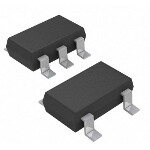
| 供应商器件封装 | TSOT-23-5 |
| 其它名称 | ADP122AUJZ-2.7-R7DKR |
| 包装 | Digi-Reel® |
| 商标 | Analog Devices |
| 安装类型 | 表面贴装 |
| 安装风格 | SMD/SMT |
| 封装 | Reel |
| 封装/外壳 | SOT-23-5 细型,TSOT-23-5 |
| 封装/箱体 | TSOT-5 |
| 工作温度 | -40°C ~ 85°C |
| 工厂包装数量 | 3000 |
| 最大工作温度 | + 125 C |
| 最大输入电压 | 5.5 V |
| 最小工作温度 | - 40 C |
| 最小输入电压 | 2.3 V |
| 标准包装 | 1 |
| 电压-跌落(典型值) | 0.085V @ 300mA |
| 电压-输入 | 最高 5.5V |
| 电压-输出 | 2.7V |
| 电流-输出 | 300mA |
| 电流-限制(最小值) | 350mA |
| 稳压器拓扑 | 正,固定式 |
| 稳压器数 | 1 |
| 系列 | ADP122 |
| 视频文件 | http://www.digikey.cn/classic/video.aspx?PlayerID=1364138032001&width=640&height=505&videoID=2245193149001 |
| 输出电流 | 300 mA |


- 商务部:美国ITC正式对集成电路等产品启动337调查
- 曝三星4nm工艺存在良率问题 高通将骁龙8 Gen1或转产台积电
- 太阳诱电将投资9.5亿元在常州建新厂生产MLCC 预计2023年完工
- 英特尔发布欧洲新工厂建设计划 深化IDM 2.0 战略
- 台积电先进制程称霸业界 有大客户加持明年业绩稳了
- 达到5530亿美元!SIA预计今年全球半导体销售额将创下新高
- 英特尔拟将自动驾驶子公司Mobileye上市 估值或超500亿美元
- 三星加码芯片和SET,合并消费电子和移动部门,撤换高东真等 CEO
- 三星电子宣布重大人事变动 还合并消费电子和移动部门
- 海关总署:前11个月进口集成电路产品价值2.52万亿元 增长14.8%


PDF Datasheet 数据手册内容提取
5.5 V Input, 300 mA, Low Quiescent Current, CMOS Linear Regulator Data Sheet ADP122/ADP123 FEATURES TYPICAL APPLICATION CIRCUITS Input voltage supply range: 2.3 V to 5.5 V VIN = 2.3VTO 5.5V VOUT = 1.8V 300 mA maximum output current 1 VIN VOUT 5 Fixed and adjustable output voltage versions 1CµIFN ADP122 C1µOFUT Very low dropout voltage: 85 mV at 300 mA load 2 GND Low quiescent current: 45 µA at no load LInoiwtia slh auctcduorwacny :c u±r1r%en atc: c<u1r aµcAy OFFON 3 EN NC 4 08399-001 Up to 31 fixed-output voltage options available from Figure 1. ADP122 with Fixed Output Voltage (TSOT Version) 1.75 V to 3.3 V Adjustable-output voltage range VIN = 2.3VTO 5.5V VOUT = 0.5V(1 + R1/R2) 1 VIN VOUT 5 0.8 V to 5.0 V (ADP123) 1CµIFN ADP123 C1µOFUT Excellent PSRR performance: 60 dB at 100 kHz 2 GND R1 Excellent load/line transient response Optimized for small 1.0 μF ceramic capacitors ON 3 EN ADJ 4 Current limit and thermal overload protection OFF LCoogmicp caoctn ptraoclkleadg eesn: a5b-lelea d TSOT and 6-lead 2 mm × 2 mm LFCSP R2 08399-002 Figure 2. ADP123 with Adjustable Output Voltage (TSOT Version) APPLICATIONS VOUT = 1.8V 1 6 VIN = 2.3V TO 5.5V Digital camera and audio devices C2 VOUT VIN C1 1µF 1µF Portable and battery-powered equipment GND 2 NC NC 5 GND Automatic meter reading (AMR) meters 3 4 ON GPS and location management units GND EN OFF Medical instrumentation GND ADP122 Point-of-sale equipment TOP VIEW GENERAL DESCRIPTION NC = NOT CONNECT.( NToHtI Sto P SINc aCleA)N BE LEFT FLOATING 08399-135 OR CONNECTED TO GROUND. The ADP122/ADP123 are low quiescent current, low dropout Figure 3. ADP122 with Fixed Output Voltage (LFCSP Version) linear regulators. They are designed to operate from an input VOUT = 0.5V (1 + R1/R2) 1 6 VIN = 2.3V TO 5.5V voltage between 2.3 V and 5.5 V and to provide up to 300 mA of C2 VOUT VIN C1 1µF R1 1µF output current. The low 85 mV dropout voltage at a 300 mA load 2 GND ADJ NC 5 GND improves efficiency and allows operation over a wide input R2 3 4 ON voltage range. GND GND EN OFF GND The low 170 μA of quiescent current at full load makes the ADP122 ADP123 TOP VIEW iTdheea lA foDrP b1a2t2te irsy c-oappaebralete odf p3o1r ftiaxbelde oequutpipumt veonltt.a ges from 1.75 V NC = NOT CONNECT. THIS P(INNo Ct AtoN SBcEa lLeE)FT FLOATING 08399-136 OR CONNECTED TO GROUND. to 3.3 V. The ADP123 is the adjustable version of the device and Figure 4. ADP123 with Adjustable Output Voltage (LFCSP Version) allows the output voltage to be set between 0.8 V and 5.0 V by The ADP122/ADP123 have an internal soft start that gives a an external voltage divider. constant start-up time of 350 µs. Short-circuit protection and The ADP122/ADP123 are specifically designed for stable operation thermal overload protection circuits prevent damage in adverse with tiny 1 µF ceramic input and output capacitors to meet the conditions. The ADP122/ADP123 are available in a tiny, 5-lead requirements of high performance, space constrained applications. TSOT package and 6-lead LFCSP package for the smallest footprint solution to meet a variety of portable applications. Rev. E Information furnished by Analog Devices is believed to be accurate and reliable. However, no responsibility is assumed by Analog Devices for its use, nor for any infringements of patents or other One Technology Way, P.O. Box 9106, Norwood, MA 02062-9106, U.S.A. rights of third parties that may result from its use. Specifications subject to change without notice. No license is granted by implication or otherwise under any patent or patent rights of Analog Devices. Tel: 781.329.4700 www.analog.com Trademarks and registered trademarks are the property of their respective owners. Fax: 781.461.3113 ©2009–2012 Analog Devices, Inc. All rights reserved.
ADP122/ADP123 Data Sheet TABLE OF CONTENTS Features .............................................................................................. 1 Theory of Operation ...................................................................... 11 Applications ....................................................................................... 1 Applications Information .............................................................. 12 General Description ......................................................................... 1 Capacitor Selection .................................................................... 12 Typical Application Circuits ............................................................ 1 Undervoltage Lockout ............................................................... 13 Revision History ............................................................................... 2 Enable Feature ............................................................................ 13 Specifications ..................................................................................... 3 Current Limit and Thermal Overload Protection ................. 14 Recommended Specifications ..................................................... 4 Thermal Considerations ............................................................ 14 Absolute Maximum Ratings ............................................................ 5 Junction Temperature Calculations For TSOT Package ....... 15 Thermal Data ................................................................................ 5 Junction Temperature Calculations For LFCSP Package ...... 17 Thermal Resistance ...................................................................... 5 Printed Circuit Board Layout Considerations........................ 19 ESD Caution .................................................................................. 5 Outline Dimensions ....................................................................... 20 Pin Configurations and Function Descriptions ........................... 6 Ordering Guide .......................................................................... 21 Typical Performance Characteristics ............................................. 7 REVISION HISTORY 6/12—Rev. D to Rev. E Added 6-Lead LFCSP Package .................................... Throughout Added Figure 3 and Figure 4 (Renumbered Sequentially) .......... 1 Changes to Table 3 ............................................................................. 5 Changes to Table 4 ............................................................................. 5 4/12—Rev. C to Rev. D Changes to Pin Configuration and Function Descriptions Changes to Ordering Guide ........................................................... 21 Section .................................................................................................6 Changes to Thermal Considerations Section ............................. 14 4/12—Rev. B to Rev. C Added Junction Temperature Calculations for LFCSP Package Changes to Operating Ambient Temperature Range; Section .............................................................................................. 17 Table 3 ................................................................................................. 5 Updated Outline Dimensions ...................................................... 20 3/12—Rev. A to Rev. B Changes to Ordering Guide .......................................................... 21 Added V = 2.8 V to Figure 23 Caption...................................... 9 10/09—Revision 0: Initial Version OUT Updated Outline Dimensions ....................................................... 20 6/11—Rev. 0 to Rev. A Rev. E | Page 2 of 24
Data Sheet ADP122/ADP123 SPECIFICATIONS Unless otherwise noted, V = (V + 0.3 V) or 2.3 V, whichever is greater; ADJ connected to VOUT; I = 10 mA; C = 1.0 µF; IN OUT OUT IN C = 1.0 µF; T = 25°C. OUT A Table 1. Parameter Symbol Test Conditions Min Typ Max Unit INPUT VOLTAGE RANGE V 2.3 5.5 V IN OPERATING SUPPLY CURRENT1 I I = 0 µA 45 µA GND OUT I = 0 µA, T = −40°C to +125°C 105 µA OUT J I = 1 mA 60 µA OUT I = 1 mA, T = −40°C to +125°C 120 µA OUT J I = 150 mA 130 µA OUT I = 150 mA, T = −40°C to +125°C 190 µA OUT J I = 300 mA 170 µA OUT I = 300 mA, T = −40°C to +125°C 240 µA OUT J SHUTDOWN CURRENT I EN = GND 0.1 µA SD EN = GND, T = −40°C to +125°C 1 µA J OUTPUT VOLTAGE ACCURACY2 V OUT Fixed Output I = 10 mA −1 +1 % OUT 100 µA < I < 300 mA, V = (V + 0.5 V) to 5.5 V, −2 +1.5 % OUT IN OUT T = −40°C to +125°C J Adjustable Output I = 10 mA 0.495 0.500 0.505 V OUT 100 µA < I < 300 mA, V = 2.3 V to 5.5 V, 0.490 0.500 0.5075 V OUT IN T = −40°C to +125°C J LINE REGULATION ∆V /∆V V = V = 2.3 V to 5.5 V, T = −40°C to +125°C −0.05 +0.05 %/V OUT IN IN IN J LOAD REGULATION3 ∆V /∆I I = 1 mA to 300 mA 0.0005 %/mA OUT OUT OUT I = 1 mA to 300 mA , T = −40°C to +125°C 0.001 %/mA OUT J ADJ INPUT BIAS CURRENT ADJ 2.3 V ≤ V ≤ 5.5 V, ADJ connected to VOUT 15 nA I-BIAS IN DROPOUT VOLTAGE4 V DROPOUT I = 10 mA, V > 2.3 V 3 mV OUT OUT I = 10 mA, T = −40°C to +125°C 5 mV OUT J I = 150 mA, V > 2.3 V 45 mV OUT OUT I = 150 mA, T = −40°C to +125°C 75 mV OUT J I = 300 mA, V > 2.3V 85 mV OUT OUT I = 300 mA, T = −40°C to +125°C 150 mV OUT J START-UP TIME5 t V = 3.0 V 350 µs START-UP OUT CURRENT LIMIT THRESHOLD6 I 350 500 650 mA LIMIT THERMAL SHUTDOWN Thermal Shutdown Threshold TS T rising 150 °C SD J Thermal Shutdown Hysteresis TS 15 °C SD-HYS EN INPUT EN Input Logic High V 2.3 V ≤ V ≤ 5.5 V 1.2 V IH IN EN Input Logic Low V 2.3 V ≤ V ≤ 5.5 V 0.4 V IL IN EN Input Leakage Current V EN = VIN or GND 0.1 µA I-LEAKAGE EN = VIN or GND, T = −40°C to +125°C 1 µA J UNDERVOLTAGE LOCKOUT UVLO Input Voltage Rising UVLO T = −40°C to +125°C 2.1 V RISE J Input Voltage Falling UVLO T = −40°C to +125°C 1.5 V FALL J Hysteresis UVLO T = 25°C 125 mV HYS A Rev. E | Page 3 of 24
ADP122/ADP123 Data Sheet Parameter Symbol Test Conditions Min Typ Max Unit OUTPUT NOISE OUT 10 Hz to 100 kHz, V = 5.5 V, V = 1.2 V 25 µV rms NOISE IN OUT 10 Hz to 100 kHz, V = 5.5 V, V = 1.8 V 35 µV rms IN OUT 10 Hz to 100 kHz, V = 5.5 V, V = 2.5 V 45 µV rms IN OUT 10 Hz to 100 kHz, V = 5.5 V, V = 3.3 V 55 µV rms IN OUT 10 Hz to 100 kHz, V = 5.5 V, V = 4.2 V 65 µV rms IN OUT POWER SUPPLY REJECTION RATIO PSRR 10 kHz, V = 3.3 V 60 dB OUT (V = V + 0.5 V) 10 kHz, V = 2.5 V 60 dB IN OUT OUT 10 kHz, V = 1.8 V 60 dB OUT 100 kHz, V = 3.3 V 60 dB OUT 100 kHz, V = 2.5 V 60 dB OUT 100 kHz, V = 1.8 V 60 dB OUT 1 The current from the external resistor divider network in the case of adjustable voltage output (as with the ADP123) should be subtracted from the ground current measured. 2 Accuracy when VOUT is connected directly to ADJ. When VOUT voltage is set by external feedback resistors, absolute accuracy in adjust mode depends on the tolerances of the resistors used. 3 Based on an endpoint calculation using 1 mA and 300 mA loads. 4 Dropout voltage is defined as the input-to-output voltage differential when the input voltage is set to the nominal output voltage. This applies only for output voltages greater than 2.3 V. 5 Start-up time is defined as the time between the rising edge of EN to VOUT being at 90% of its nominal value. 6 Current limit threshold is defined as the current at which the output voltage drops to 90% of the specified typical value. For example, the current limit for a 3.3 V output voltage is defined as the current that causes the output voltage to drop to 90% of 3.3V, or 2.97 V. RECOMMENDED SPECIFICATIONS Table 2. Parameter Symbol Test Conditions Min Typ Max Unit Minimum Input and Output CAP T = −40°C to +125°C 0.70 µF MIN A Capacitance1 Capacitor ESR R T = −40°C to +125°C 0.001 1 Ω ESR A 1 The minimum input and output capacitance should be greater than 0.70 µF over the full range of operating conditions. The full range of operating conditions in the application must be considered during device selection to ensure that the minimum capacitance specification is met. X7R and X5R type capacitors are recommended; Y5V and Z5U capacitors are not recommended for use with any LDO. Rev. E | Page 4 of 24
Data Sheet ADP122/ADP123 ABSOLUTE MAXIMUM RATINGS application and board layout. In applications in which high maxi- Table 3. mum power dissipation exists, close attention to thermal board Parameter Rating design is required. The value of θ may vary, depending on PCB VIN to GND −0.3 V to +6.5 V JA material, layout, and environmental conditions. The specified ADJ to GND −0.3 V to +6.5 V values of θ are based on a 4-layer, 4 inch × 3 inch circuit board. EN to GND −0.3 V to +6.5 V JA Refer to JESD51-7 for detailed information on the board VOUT to GND −0.3 V to VIN construction Storage Temperature Range −65°C to +150°C Operating Ambient Temperature Range −40°C to +125°C Ψ is the junction-to-board thermal characterization parameter JB Operating Junction Temperature −40°C to +125°C and is measured in °C/W. The Ψ of the package is based on JB Soldering Conditions JEDEC J-STD-020 modeling and calculation using a 4-layer board. The Guidelines for Reporting and Using Package Thermal Information: JESD51-12 states that thermal characterization parameters are not the same Stresses above those listed under Absolute Maximum Ratings may as thermal resistances. Ψ measures the component power flowing cause permanent damage to the device. This is a stress rating JB through multiple thermal paths rather than a single path as in only; functional operation of the device at these or any other thermal resistance, θ . Therefore, Ψ thermal paths include conditions above those indicated in the operational section of JB JB convection from the top of the package as well as radiation from this specification is not implied. Exposure to absolute maximum the package—factors that make Ψ more useful in real-world rating conditions for extended periods may affect device reliability. JB applications. Maximum junction temperature (T) is calculated J THERMAL DATA from the board temperature (T ) and power dissipation (P ) B D Absolute maximum ratings apply individually only, not in using the formula combination. The ADP122/ADP123 can be damaged when the T = T + (P × Ψ ) J B D JB junction temperature limits are exceeded. Monitoring ambient Refer to JESD51-8 and JESD51-12 for more detailed information temperature does not guarantee that T will remain within the J about Ψ . specified temperature limits. In applications with high power JB dissipation and poor thermal resistance, the maximum ambient THERMAL RESISTANCE temperature may have to be derated. θ and Ψ are specified for the worst-case conditions, that is, a JA JB In applications with moderate power dissipation and low PCB device soldered in a circuit board for surface-mount packages. thermal resistance, the maximum ambient temperature can Table 4. Thermal Resistance exceed the maximum limit as long as the junction temperature Package Type θ Ψ Unit is within specification limits. The junction temperature (T) of JA JB J 5-Lead TSOT 170 43 °C/W the device is dependent on the ambient temperature (T ), the A 6-Lead 2 mm × 2 mm LFCSP 68.9 44.1 °C/W power dissipation of the device (P ), and the junction-to-ambient D thermal resistance of the package (θ ). JA ESD CAUTION Maximum junction temperature (T) is calculated from the J ambient temperature (T ) and power dissipation (P ) using the A D formula T = T + (P × θ ) J A D JA The junction-to-ambient thermal resistance (θ ) of the package JA is based on modeling and calculation using a 4-layer board. The junction-to-ambient thermal resistance is highly dependent on the Rev. E | Page 5 of 24
ADP122/ADP123 Data Sheet PIN CONFIGURATIONS AND FUNCTION DESCRIPTIONS VIN 1 5 VOUT VIN 1 5 VOUT ADP122 ADP123 GND 2 (NToOt Pto V SIEcWale) GND 2 TOPVIEW EN 3NC = NO CONNECT4 NC 08399-004 EN 3 (NottoScale) 4 ADJ 08399-003 Figure 5. ADP122 TSOT Fixed Output Pin Configuration Figure 7. ADP123 TSOT Adjustable Output Pin Configuration ADP122 ADP123 TOP VIEW TOP VIEW (Not to Scale) (Not to Scale) 1 VOUT VIN 6 1 VOUT VIN 6 2 NC NC 5 2 ADJ NC 5 3 GND EN 4 3 GND EN 4 NOTES NOTES 1 2 .. NEOXCRP =CO ONSONENTD E CPCOATNDEN DME UTCOSTT .G TBRHEOI SCU OPNINDNN. CEACNT EBDE TLOE FGTN FDL.OATING08399-137 1 2 .. NEOXCRP =CO ONSONENTD E CPCOATNDEN DME UTCOSTT .G TBRHEOI SCU OPNINDNN. CEACNT EBDE TLOE FGTN FDL.OATING08399-138 Figure 6. ADP122 LFCSP Fixed Output Pin Configuration Figure 8. ADP123 LFCSP Adjustable Output Pin Configuration Table 5. Pin Function Descriptions Pin No. ADP122 ADP123 TSOT LFCSP TSOT LFCSP Mnemonic Description 1 6 1 6 VIN Regulator Input Supply. Bypass VIN to GND with a capacitor of at least 1 µF. 2 3 2 3 GND Ground. 3 4 3 4 EN Enable Input. Drive EN high to turn on the regulator; drive EN low to turn off the regulator. For automatic startup, connect EN to VIN. N/A N/A 4 2 ADJ Output Voltage Adjust Input. Connect the midpoint of an external divider from VOUT to GND to this pin to set the output voltage. 4 2, 5 N/A 5 NC No Connect. These pins are not internally bonded. They can be left floating or connected to ground. 5 1 5 1 VOUT Regulated Output Voltage. Bypass VOUT to GND with a capacitor of at least 1 µF. N/A EP N/A EP EPAD Exposed Pad. The exposed pad must be connected to ground. Rev. E | Page 6 of 24
Data Sheet ADP122/ADP123 TYPICAL PERFORMANCE CHARACTERISTICS V = 3.6 V, V = 3.3 V, I = 10 mA, C = 1.0 µF, C = 1.0 µF, T = 25°C, unless otherwise noted. IN OUT OUT IN OUT A 3.300 250 3.295 200 (V)OUT333...222889050 IIOOUUTT == 110m0AµA CURRENT (µA)150 IIIOOOUUUTTT === 123000000mmmAAA V IOUT = 10mA D 3.275 IOUT = 100mA UN100 IIOOUUTT == 230000mmAA GRO IOUT = 10mA 3.270 50 3.265 IOUT = 100µA IOUT = 1mA 3.260 –40 JU–N5CTION TEM25PERATURE8 (5°C) 125 08399-005 0 –40 JU–N5CTION TEM25PERATURE8 5(°C) 125 08399-008 Figure 9. Output Voltage vs. Junction Temperature Figure 12. Ground Current vs. Junction Temperature 3.2945 200 3.2940 180 3.2935 160 3.2930 µA)140 T ( V) 3.2925 REN120 (OUT3.2920 CUR100 V D 3.2915 N 80 U O 3.2910 R 60 G 3.2905 40 3.2900 20 3.28950.1 1 IOUT1 0(mA) 100 1000 08399-006 00.1 1 IOUT 1(0mA) 100 1000 08399-009 Figure 10. Output Voltage vs. Load Current Figure 13. Ground Current vs. Load Current 3.296 200 180 IOUT = 300mA 3.294 160 3.292 T (µA)140 IOUT = 200mA (V)UT3.290 URREN110200 IOUT = 100mA O C V ND 80 IOUT = 10mA U 3.288 IOUT = 100µA GRO 60 IOUT = 1mA 3.286 IIIOOOUUUTTT === 111m00m0AmAA 40 IOUT = 100µA IOUT = 200mA 20 IOUT = 300mA 3.2843.6 3.8 4.0 4.2 4.V4IN (V4).6 4.8 5.0 5.2 5.4 08399-007 03.6 3.8 4.0 4.2 4.4VIN 4(V.6) 4.8 5.0 5.2 5.4 08399-010 Figure 11. Output Voltage vs. Input Voltage Figure 14. Ground Current vs. Input Voltage Rev. E | Page 7 of 24
ADP122/ADP123 Data Sheet 0.50 3.35 0.45 3.30 T (µA)0.40 VIN = 3.6V 3.25 IIIOOOUUUTTT === 111005m00mmAAA EN0.35 VIN = 3.8V IOUT = 300mA N CURR0.30 VVVIIINNN === 445...240VVV (V)OUT3.20 W VIN = 5.2V V 3.15 DO0.25 VIN = 5.4V SHUT0.20 VIN = 5.5V 3.10 3.05 0.15 0.10–50 –25 0 TE2M5PERAT5U0RE (°C7)5 100 125 08399-011 3.003.05 3.10 3.15 3.20VIN (V3).25 3.30 3.35 3.40 08399-013 Figure 15. Shutdown Current vs. Temperature at Various Input Voltages Figure 18. Output Voltage vs. Input Voltage (in Dropout) 70 –10 –20 60 IOUT = 100µA –30 IOUT = 1mA 50 IOUT = 10mA V) –40 IOUT = 100mA ROPOUT (m3400 PSRR (dB) ––6500 IIOOUUTT == 230000mmAA D –70 20 –80 10 VIN = VOUT + 0.5V 01 10 IOUT (mA) 100 1000 08399-012 ––1900010 CVRIN1IP 0=P0 LCEO =U T5 01mµ1FkVFREQU1E0NkCY (Hz)100k 1M 10M08399-015 Figure 16. Dropout Voltage vs. Load Current Figure 19. Power Supply Rejection Ratio vs. Frequency, V = 2.8 V, V = 3.3 V OUT IN 450 –10 400 –20 350 –30 IIOOUUTT == 110m0AµA 300 –40 IIOOUUTT == 1100m0mAA (µA)GND220500 SRR (dB) ––6500 IIOOUUTT == 230000mmAA I P 150 –70 100 IOUT= 10mA –80 5003.05 3.10IIIOOOUUUTTT3===.1 1135050000mmm3AAA.20 V3IN.2 (5V) 3.30 3.35 3.40 3.45 08399-014 ––1900010 CVVIRINN1I P 0==P0 LVCEOO =UU TT5 +01m µ01F.kV5FVREQU1E0NkCY (Hz)100k 1M 10M08399-016 Figure 17. Ground Current vs. Input Voltage (in Dropout) Figure 20. Power Supply Rejection Ratio vs. Frequency, V = 3.3 V, V = 3.8 V OUT IN Rev. E | Page 8 of 24
Data Sheet ADP122/ADP123 –10 5 –20 –30 IIOOUUTT == 110m0AµA 4 VOUT = 4.2V –40 IIOOUUTT == 1100m0mAA Hz) VOUT = 3.3V R (dB) –50 IIOOUUTT == 230000mmAA E(µv/√ 3 PSR –60 NOIS 2 –70 –––1980000 CVVIRINNI P ==P LVCEOO =UU TT5 +01m µ0F.V5V 08399-017 01 VOUT = 2.8V 08399-020 10 100 1k 10k 100k 10 100 1k 10k 100k 1M 10M FREQUENCY (Hz) FREQUENCY (Hz) Figure 21. Power Supply Rejection Ratio vs. Frequency, V = 4.2 V, V = 4.7 V Figure 24. Output Noise Spectrum OUT IN –10 70 –20 VOUT = 2.8V, IOUT = 1mA 65 VOUT = 4.2V –30 VOUT = 3.3V, IOUT = 1mA VOUT = 4.2V, IOUT = 1mA 60 dB) ––5400 VVVOOOUUUTTT === 234...832VVV,,, IIIOOOUUUTTT === 333000000mmmAAA SE (µV)55 VOUT = 3.3V R ( OI50 R N S –60 S P M –70 R45 VOUT = 2.8V 40 –80 VIN = VOUT + 0.5V VRIPPLE = 50mV ––19000 CIN = COUT 1µF 08399-018 3305 08399-021 10 100 1k 10k 100k 1M 10M 0.001 0.01 0.1 1 10 100 1000 FREQUENCY (Hz) IOUT (mA) Figure 22. Power Supply Rejection Ratio vs. Frequency, Various Output Figure 25. Output Noise vs. Load Current and Output Voltage Voltages and Load Currents –10 –20 VVVIIINNN === 333...138VVV,,, IIIOOOUUUTTT === 111mmmAAA IOUT VIN = 4.8V, IOUT = 1mA 1mA TO 300mA LOAD STEP –30 VIN = 3.1V, IOUT = 300mA 1 VIN = 3.3V, IOUT = 300mA –40 VIN = 3.8V, IOUT = 300mA VIN = 4.8V, IOUT = 300mA B) d –50 R ( R PS –60 2 VOUT –70 –80 VRIPPLE = 50mV ––1900010 C1I0N0 = COUT 11µkF 10k 100k 1M 10M08399-019 CH1 200mA ΩBWCH2 50.0mV BW M 40.0µs AVV CIONHU 1=T 3= . 73 V1.39V6mA 08399-022 T 10.20% FREQUENCY (Hz) Figure 23. Power Supply Rejection Ratio vs. Headroom Voltage (V − V ), Figure 26. Load Transient Response, C = 1 μF IN OUT OUT V = 2.8 V OUT Rev. E | Page 9 of 24
ADP122/ADP123 Data Sheet IOUT VIN 1mA TO 300mA LOAD STEP 1 4V TO 4.5V VOLTAGE STEP 2 VOUT 2 VOUT 1 VVIONU =T 3=. 73V.3V 08399-023 08399-025 CH1 200mA ΩBWCH2 20.0mV BWM 40.0µs A CH1 196mA CH1 1.00VBW CH2 2.00mV BW M 10.0µs A CH3 2.04V T 10.40% T 9.600% Figure 27. Load Transient Response, C = 4.7 μF Figure 29. Line Transient Response, Load Current = 300 mA OUT VIN 4V TO 4.5V VOLTAGE STEP 2 VOUT 1 08399-024 CH1 1.00V ΩBW CH2 2.00mV BW M 10.0µs A CH3 2.04V T 10.00% Figure 28. Line Transient Response, Load Current = 1 mA Rev. E | Page 10 of 24
Data Sheet ADP122/ADP123 THEORY OF OPERATION The ADP122/ADP123 are low quiescent current, low-dropout Note that in shutdown, the output is turned off and the divider linear regulators that operate from 2.3 V to 5.5 V and can provide current is 0. up to 300 mA of output current. Drawing a low 170 µA of quies- The ADP122/ADP123 use the EN pin to enable and disable the cent current (typical) at full load makes the ADP122/ADP123 VOUT pin under normal operating conditions. When EN is high, ideal for battery-operated portable equipment. Shutdown current VOUT turns on; when EN is low, VOUT turns off. For automatic consumption is typically 100 nA. startup, EN can be tied to VIN. Optimized for use with small 1 µF ceramic capacitors, the ADP122 ADP122/ADP123 provide excellent transient performance. VIN VOUT Internally, the ADP122/ADP123 consist of a reference, an error amplifier, a feedback voltage divider, and a PMOS pass transistor. Output current is delivered via the PMOS pass device, which is SHORT CIRCUIT, R1 GND UVLOAND controlled by the error amplifier. The error amplifier compares THERMAL the reference voltage with the feedback voltage from the output PROTECT and amplifies the difference. If the feedback voltage is lower than the reference voltage, the gate of the PMOS device is pulled lower, EN SHUTDOWN 0.5V REFERENCE R2 allowing more current to pass and increasing the output voltage. Igfa tthe eo ffe tehdeb PaMckO vSo ldtaegvei cies hisi gphuellre tdh hanig thheer ,r aelfleorwenincge lveoslst acguer,r tehnet 08399-121 NOTES to pass and decreasing the output voltage. 1. R1AND R2ARE INTERNAL RESISTORS,AVAILABLE ON THEADP122 ONLY. The adjustable ADP123 has an output voltage range of 0.8 V to Figure 30. ADP122 Internal Block Diagram (Fixed Output) 5.0 V. The output voltage is set by the ratio of two external resistors, as shown in Figure 2. The device servos the output to maintain ADP123 the voltage at the ADJ pin at 0.5 V referenced to ground. The VIN VOUT current in R1 is then equal to 0.5 V/R2 and the current in R1 is the current in R2 plus the ADJ pin bias current. The ADJ pin bias current, 15 nA at 25°C, flows through R1 into the ADJ pin. SHORT CIRCUIT, GND UVLOAND The output voltage can be calculated using the equation: THERMAL PROTECT V = 0.5 V(1 + R1/R2) + (ADJ )(R1) OUT I-BIAS ADJ The value of R1 should be less than 200 kΩ to minimize errors EN SHUTDOWN 0.5V REFERENCE in the output voltage caused by the ADJ pin bias current. For eisx 1am.0 pVle. ,T whhee onu Rtp1u at nvdo lRta2g eea ecrhr oerq uinatlr 2o0d0u kceΩd, bthye t ohue tApuDt Jv poilnta ge 08399-122 Figure 31. ADP123 Internal Block Diagram (Adjustable Output) bias current is 3 mV or 0.3%, assuming a typical ADJ pin bias current of 15 nA at 25°C. Rev. E | Page 11 of 24
ADP122/ADP123 Data Sheet APPLICATIONS INFORMATION CAPACITOR SELECTION Input and Output Capacitor Properties Output Capacitor Any good quality ceramic capacitors can be used with the ADP122/ ADP123, as long as the capacitor meets the minimum capacitance The ADP122/ADP123 are designed for operation with small, and maximum ESR requirements. Ceramic capacitors are manu- space-saving ceramic capacitors, but these devices can function factured with a variety of dielectrics, each with different behavior with most commonly used capacitors as long as care is taken to over temperature and applied voltage. Capacitors must have an ensure an appropriate effective series resistance (ESR) value. The adequate dielectric to ensure the minimum capacitance over the ESR of the output capacitor affects the stability of the LDO control necessary temperature range and dc bias conditions. Using an loop. A minimum of 0.70 µF capacitance with an ESR of 1 Ω or X5R or X7R dielectric with a voltage rating of 6.3 V or 10 V is less is recommended to ensure stability of the ADP122/ADP123. recommended. However, using Y5V and Z5U dielectrics is not The transient response to changes in load current is also affected by recommended for any LDO, due to their poor temperature and the output capacitance. Using a larger value of output capacitance dc bias characteristics. improves the transient response of the ADP122/ADP123 to dynamic changes in load current. Figure 32 and Figure 33 show Figure 34 depicts the capacitance vs. capacitor voltage bias charac- the transient responses for output capacitance values of 1 µF and teristics of a 0603, 1 µF, 6.3 V X5R capacitor. The voltage stability of 4.7 µF, respectively. a capacitor is strongly influenced by the capacitor size and the voltage rating. In general, a capacitor in a larger package or of a IOUT higher voltage rating exhibits better stability. The temperature 1mA TO 300mA LOAD STEP variation of the X5R dielectric is about ±15% over the −40°C to 1 +85°C temperature range and is not a function of package or voltage rating. 1.10 1.05 2 VOUT 1.00 F) E (µ0.95 VVIONU =T 3=. 73V.3V 08399-026 CITANC0.90 CH1 200mAΩBW CH2 50.0mV BW MT 4 0 0 n1s4.8A0 % CH1 196mA CAPA0.85 Figure 32. Output Transient Response, COUT = 1 µF 0.80 IOUT 00..7705 08399-030 0 1 2 3 4 5 6 7 1mA TO 300mA LOAD STEP 1 BIAS VOLTAGE (V) Figure 34. Capacitance vs. Capacitor Voltage Bias Characteristics Equation 1 can be used to determine the worst-case capacitance, accounting for capacitor variation over temperature, component tolerance, and voltage. 2 C = C × (1 − TEMPCO) × (1 − TOL) (1) EFF VOUT where: VVIONU =T 3=. 73V.3V 08399-027 CTEEFMF iPs CthOe iesf ftehcet iwveo rcsatp-caacsitea ncacpea acti ttohre toepmepraetriantgu rveo cltoaegfef.i cient. CH1 200mA ΩBW CH2 20.0mV M 400ns A CH1 196mA TOL is the worst-case component tolerance. T 15.00% Figure 33. Output Transient Response, COUT = 4.7 µF In this example, the worst-case temperature coefficient (TEMPCO) Input Bypass Capacitor over −40°C to +85°C is assumed to be 15% for an X5R dielectric. The tolerance of the capacitor (TOL) is assumed to be 10%, and Connecting a 1 µF capacitor from VIN to GND reduces the circuit C is 0.96 μF at 4.2 V from the graph in Figure 34. sensitivity to the printed circuit board (PCB) layout, especially when a long input trace or high source impedance is encountered. Substituting these values in Equation 1 yields If greater than 1 µF of output capacitance is required, the input C = 0.96 μF × (1 − 0.15) × (1 − 0.1) = 0.734 μF EFF capacitor should be increased to match it. Rev. E | Page 12 of 24
Data Sheet ADP122/ADP123 Therefore, the capacitor chosen in this example meets the 1.1 minimum capacitance requirement of the LDO over tem- perature and tolerance at the chosen output voltage. 1.0 V) To guarantee the performance of the ADP122/ADP123, it is DS (0.9 RISING imperative that the effects of dc bias, temperature, and tolerances L O H on the behavior of the capacitors are evaluated for each application. S RE0.8 UNDERVOLTAGE LOCKOUT TH FALLING E L The ADP122/ADP123 have an internal undervoltage lockout AB0.7 N circuit that disables all inputs and the output when the input E 0.6 voltage is less than approximately 2 V. This ensures that the ADP122/ADP123 inputs and the output behave in a predictable 0.5 mENanAnBerL dEu FriEnAg pToUwRerE- up. 2.2 2.7 3.2 3.7VIN(V) 4.2 4.7 5.2 08399-034 Figure 36. Typical EN Pin Thresholds vs. Input Voltage The ADP122/ADP123 uses the EN pin to enable and disable the VOUT pin under normal operating conditions. As shown in The ADP122/ADP123 utilize an internal soft start to limit the Figure 35, when a rising voltage on EN crosses the active threshold, in-rush current when the output is enabled. The start-up time VOUT turns on. Conversely, when a falling voltage on EN crosses for the 2.8 V option is approximately 350 µs from the time the the inactive threshold, VOUT turns off. EN active threshold is crossed to when the output reaches 90% of its final value. As shown in Figure 37, the start-up time is 3.5 dependent on the output voltage setting and increases slightly 3.0 as the output voltage increases. 2.5 VIN = 5V 2.0 VOUT = 4.2V UT VO VOUT = 3.3V 1.5 VOUT = 2.8V 1.0 0.5 0 08399-230 21 0 0.2 0.4 0.6 0.8 1.0 1.2 1.4 1.6 Figure 35. Typical EVNEN Pin Operation 08399-033 CH1 1.00V CH2 1.00V M200µs A CH1 3.08V As shown in Figure 35, the EN pin has built-in hysteresis. This T 600.000µs prevents on/off oscillations that may occur due to noise on the Figure 37. Typical Start-Up Time EN pin as it passes through the threshold points. The active and inactive thresholds of the EN pin are derived from the VIN voltage. Therefore, these thresholds vary as the input voltage changes. Figure 36 shows typical EN active and inactive thresholds when the VIN voltage varies from 2.3 V to 5.5 V. Rev. E | Page 13 of 24
ADP122/ADP123 Data Sheet CURRENT LIMIT AND THERMAL OVERLOAD Table 6. Typical θ Values for Specified PCB Copper Sizes PROTECTION JA θ (°C/W) JA The ADP122/ADP123 are protected from damage due to excessive Copper Size (mm2) TSOT LFCSP power dissipation by current and thermal overload protection 01 170 255 circuits. The ADP122/ADP123 are designed to limit the current 50 152 164 when the output load reaches 500 mA (typical). When the output 100 146 138 load exceeds 500 mA, the output voltage is reduced to maintain 300 134 109 a constant current limit. 500 131 80 Thermal overload protection is included, which limits the junction 1 Device soldered to narrow traces. temperature to a maximum of 150°C typical. Under extreme con- ditions (that is, high ambient temperature and power dissipation), The typical ΨJB values are 42.8°C/W for TSOT packages and when the junction temperature starts to rise above 150°C, the 44.1°C/W for LFCSP packages. output is turned off, reducing output current to zero. When the The junction temperature of the ADP122/ADP123 can be junction temperature cools to less than 135°C, the output is turned calculated from the following equation: on again and the output current is restored to its nominal value. T = T + (P × θ ) (2) J A D JA Consider the case where a hard short from VOUT to GND occurs. where: At first, the ADP122/ADP123 limit the current so that only 500 mA T is the ambient temperature. is conducted into the short. If self-heating causes the junction A P is the power dissipation in the die, given by temperature to rise above 150°C, thermal shutdown activates, D turning off the output and reducing the output current to zero. PD = [(VIN − VOUT) × ILOAD] + (VIN × IGND) (3) When the junction temperature cools to less than 135°C, the where: output turns on and conducts 500 mA into the short, again I is the load current. LOAD causing the junction temperature to rise above 150°C. This I is the ground current. GND thermal oscillation between 135°C and 150°C results in a current V and V are input and output voltages, respectively. IN OUT oscillation between 500 mA and 0 mA that continues as long as The power dissipation due to ground current is quite small and the short remains at the output. can be ignored. Therefore, the junction temperature equation Current and thermal limit protections are intended to protect the can be simplified as follows: device from damage due to accidental overload conditions. For T = T + {[(V − V ) × I ] × θ } (4) reliable operation, the device power dissipation must be externally J A IN OUT LOAD JA limited so that the junction temperature does not exceed 125°C. As shown in Equation 4, for a given ambient temperature, input- to-output voltage differential, and continuous load current, there THERMAL CONSIDERATIONS exists a minimum copper size requirement for the PCB to ensure To guarantee reliable operation, the junction temperature of the that the junction temperature does not rise above 125°C. Figure 38 ADP122/ADP123 must not exceed 125°C. To ensure that the through Figure 44 show junction temperature calculations for junction temperature is less than this maximum value, the user different ambient temperatures, load currents, V to V IN OUT needs to be aware of the parameters that contribute to junction differentials, and areas of PCB copper. temperature changes. These parameters include ambient tem- In cases where the board temperature is known, the thermal perature, power dissipation in the power device, and thermal characterization parameter, Ψ , can be used to estimate the jun- resistances between the junction and ambient air (θ ). The value JB JA ction temperature rise. The maximum junction temperature (T) is of θ is dependent on the package assembly compounds used J JA calculated from the board temperature (T) and power dissipation and the amount of copper to which the GND pins of the package B (P ) using the formula are soldered on the PCB. Table 6 shows typical θ values of the D JA 5-lead TSOT package and 6-lead LFCSP package for various TJ = TB + (PD × ΨJB) (5) PCB copper sizes. Rev. E | Page 14 of 24
Data Sheet ADP122/ADP123 JUNCTION TEMPERATURE CALCULATIONS FOR TSOT PACKAGE 140 140 TJ MAX TJ MAX 120 120 C) C) E (° 100 ILOAD = 300mA E (° 100 ILOAD = 300mA R R U U T T A A ER 80 ILOAD = 150mA ER 80 ILOAD = 150mA P P M M E E ON T 60 ILOAD = 100mA ON T 60 ILOAD = 100mA NCTI 40 ILOAD = 25mA NCTI 40 ILOAD = 25mA U U J J 20 20 ILOAD = 1mA ILOAD = 10mA ILOAD = 1mA ILOAD = 10mA 00.5 1.0 1V.5OUT – VIN (2V.)0 2.5 3.0 08399-128 00.5 1.0 1V.5OUT – VIN (2V.)0 2.5 3.0 08399-130 Figure 38. Junction Temperature vs. Power Dissipation, Figure 40. Junction Temperature vs. Power Dissipation, 500 mm2 of PCB Copper, T = 25°C 0 mm2 of PCB Copper, T = 25°C A A 140 140 TJ MAX TJ MAX 120 120 E (°C) 100 ILOAD = 300mA E (°C) 100 ILOAD = 300mA ILOAD = 150mA R R U U T T PERA 80 ILOAD = 150mA PERA 80 ILOAD = 100mA M M TE 60 TE 60 ILOAD = 25mA ON ILOAD = 100mA ON TI TI UNC 40 ILOAD = 25mA UNC 40 ILOAD = 1mA ILOAD = 10mA J J 20 20 ILOAD = 1mA ILOAD = 10mA 00.5 1.0 1V.5OUT – VIN (2V.)0 2.5 3.0 08399-129 00.5 1.0 1V.5OUT – VIN (2V.)0 2.5 3.0 08399-131 Figure 39. Junction Temperature vs. Power Dissipation, Figure 41. Junction Temperature vs. Power Dissipation, 100 mm2 of PCB Copper, T = 25°C 500 mm2 of PCB Copper, T = 50°C A A Rev. E | Page 15 of 24
ADP122/ADP123 Data Sheet 140 140 TJ MAX 120 120 MPERATURE (°C) 10800 ILOAD = 300mA ILOAD = 150mA ILOAD = 100mA MPERATURE (°C) 10800 JUNCTION TE 6400 ILOIALDO A=D 1 =m 2A5mA ILOAD = 10mA JUNCTION TE 6400 IIIILLLLOOOOAAAADDDD ==== 1151m000mm0AmAAA IIITLLLJOOO MAAADDDA X=== 123550000mmmAAA 20 20 00.5 1.0 1V.5OUT – VIN (2V.)0 2.5 3.0 08399-132 00.4 0.8 1.2 VIN – 1V.O6UT (V) 2.0 2.4 2.8 08399-134 Figure 42. Junction Temperature vs. Power Dissipation, Figure 44. Junction Temperature vs. Power Dissipation, 100 mm2 of PCB Copper, T = 50°C Board Temperature = 85°C A 140 TJ MAX 120 E (°C) 100 ILOAD = 300mA ILOAD = 150mA R U T RA 80 ILOAD = 100mA E P EM ILOAD = 25mA T 60 N O TI C 40 UN ILOAD = 1mA ILOAD = 10mA J 20 00.5 1.0 1V.5OUT – VIN (2V.)0 2.5 3.0 08399-133 Figure 43. Junction Temperature vs. Power Dissipation, 0 mm2 of PCB Copper, T = 50°C A Rev. E | Page 16 of 24
Data Sheet ADP122/ADP123 JUNCTION TEMPERATURE CALCULATIONS FOR LFCSP PACKAGE 140 140 TJMAX TJMAX 120 120 C) C) 300mA (° (° E 100 E 100 R R U U AT 300mA AT 150mA R 80 R 80 PE PE 100mA M M TE 60 150mA TE 60 25mA N N O 100mA O TI TI C 40 C 40 UN 25mA UN 1mA 10mA J J 20 20 1mA 10mA 0 0 0.5 1.0 1V.5OUT–VIN(V2.)0 2.5 3.0 08399-139 0.5 1.0 1V.5OUT–VIN(V2.)0 2.5 3.0 08399-141 Figure 45. Junction Temperature vs. Power Dissipation, Figure 47. Junction Temperature vs. Power Dissipation, 500 mm2 of PCB Copper, T = 25°C 500 mm2 of PCB Copper, T = 50°C A A 140 140 TJMAX TJMAX 120 120 E(°C) 100 300mA E(°C) 100 300mA 150mA R R ATU ATU 100mA R 80 R 80 E E P P M 150mA M TE 60 100mA TE 60 25mA N N O O UNCTI 40 25mA UNCTI 40 1mA 10mA J J 20 20 10mA 1mA 0 0 0.5 1.0 1V.5OUT–VIN(V2.)0 2.5 3.0 08399-140 0.5 1.0 1V.5OUT–VIN(V2.)0 2.5 3.0 08399-142 Figure 46. Junction Temperature vs. Power Dissipation, Figure 48. Junction Temperature vs. Power Dissipation, 100 mm2 of PCB Copper, T = 25°C 100 mm2 of PCB Copper, T = 50°C A A Rev. E | Page 17 of 24
ADP122/ADP123 Data Sheet 140 140 TJMAX TJMAX 120 120 )C 300mA 150mA C) 300mA (° (° 150mA E 100 E 100 R R U 100mA U 100mA AT AT R 80 R 80 E E MP MP 1mA 10mA E E 25mA T 60 T 60 N N O O TI 25mA TI C 40 C 40 N N U U J J 20 20 10mA 1mA 0 0 0.5 1.0 1V.5OUT–VIN(V2.)0 2.5 3.0 08399-143 0.4 0.8 1.2 VOUT1–.6VIN(V) 2.0 2.4 2.8 08399-144 Figure 49. Junction Temperature vs. Power Dissipation, Figure 51. Junction Temperature vs. Power Dissipation, 0 mm2 of PCB Copper, T = 25°C Board Temperature = 85°C A 140 TJMAX 120 C) 300mA 150mA (° E 100 UR 100mA T A R 80 E MP 25mA E T 60 N O TI C 40 10mA UN 1mA J 20 0 0.5 1.0 1V.5OUT–VIN(V2.)0 2.5 3.0 08399-145 Figure 50. Junction Temperature vs. Power Dissipation, 0 mm2 of PCB Copper, T = 50°C A Rev. E | Page 18 of 24
Data Sheet ADP122/ADP123 PRINTED CIRCUIT BOARD LAYOUT CONSIDERATIONS Heat dissipation from the package can be improved by increasing The input capacitor should be placed as close as possible to the the amount of copper attached to the pins of the ADP122/ADP123. VIN and GND pins, and the output capacitor should be placed However, as shown in Table 6, a point of diminishing returns as close as possible to the VOUT and GND pins. Use of 0402 or eventually is reached, beyond which an increase in the copper 0603 size capacitors and resistors achieves the smallest possible size does not yield significant heat dissipation benefits. footprint solution on boards where the area is limited. 08399-041 Figure 52. Example ADP122 PCB Layout 08399-042 Figure 53. Example ADP123 PCB Layout Rev. E | Page 19 of 24
ADP122/ADP123 Data Sheet OUTLINE DIMENSIONS 2.90 BSC 5 4 1.60 BSC 2.80 BSC 1 2 3 0.95 BSC 1.90 *0.90 MAX BSC 0.70 MIN *1.00 MAX 0.20 0.08 8° 0.10 MAX 0.50 SEATING 4° 0.60 0.30 PLANE 0° 0.45 0.30 *CTHOEM PELXICAENPTT TIOON J OEDF EPCA CSTKAANGDEA HREDIGS HMTO A-1N9D3 -TAHBICWKINTHESS. 100708-A Figure 54. 5-Lead Thin Small Outline Transistor Package [TSOT] (UJ-5) Dimensions shown in millimeters 1.70 1.60 2.00 1.50 BSC SQ 0.65 BSC 4 6 0.175 REF PIN 1 INDEX EXPOSED 1.10 AREA PAD 1.00 0.425 0.90 0.350 0.275 3 1 PIN 1 TOP VIEW BOTTOM VIEW INDICATOR (R 0.15) 0.60 FOR PROPER CONNECTION OF 0.55 0.05 MAX THE EXPOSED PAD, REFER TO THE PIN CONFIGURATION AND 0.50 0.02 NOM FUNCTION DESCRIPTIONS SECTION OF THIS DATA SHEET. SEPALTAINNGE 000...332505 0.20 REF 07-11-2011-B Figure 55. 6-Lead Lead Frame Chip Scale Package [LFCSP_UD] 2.00 mm× 2.00 mm Body, Ultra Thin, Dual Lead (CP-6-3) Dimensions shown in millimeters Rev. E | Page 20 of 24
Data Sheet ADP122/ADP123 ORDERING GUIDE Model1 Temperature Range Output Voltage (V)2 Package Description Package Option Branding ADP122AUJZ-1.8-R7 –40°C to +125°C 1.8 5-Lead TSOT UJ-5 LJS ADP122AUJZ-2.5-R7 –40°C to +125°C 2.5 5-Lead TSOT UJ-5 LE6 ADP122AUJZ-2.7-R7 –40°C to +125°C 2.7 5-Lead TSOT UJ-5 LE9 ADP122AUJZ-2.8-R7 –40°C to +125°C 2.8 5-Lead TSOT UJ-5 LEA ADP122AUJZ-2.85-R7 –40°C to +125°C 2.85 5-Lead TSOT UJ-5 LEC ADP122AUJZ-2.9-R7 –40°C to +125°C 2.9 5-Lead TSOT UJ-5 LED ADP122AUJZ-3.0-R7 –40°C to +125°C 3.0 5-Lead TSOT UJ-5 LEE ADP122AUJZ-3.3-R7 –40°C to +125°C 3.3 5-Lead TSOT UJ-5 LEF ADP122ACPZ-1.8-R7 –40°C to +125°C 1.8 6-Lead LFCSP_UD CP-6-3 LJS ADP122ACPZ-2.0-R7 –40°C to +125°C 2.0 6-Lead LFCSP_UD CP-6-3 LJT ADP122ACPZ-2.5-R7 –40°C to +125°C 2.5 6-Lead LFCSP_UD CP-6-3 LE6 ADP122ACPZ-2.6-R7 –40°C to +125°C 2.6 6-Lead LFCSP_UD CP-6-3 LJU ADP122ACPZ-2.8-R7 –40°C to +125°C 2.8 6-Lead LFCSP_UD CP-6-3 LEA ADP122ACPZ-3.0-R7 –40°C to +125°C 3.0 6-Lead LFCSP_UD CP-6-3 LEE ADP122ACPZ-3.3-R7 –40°C to +125°C 3.3 6-Lead LFCSP_UD CP-6-3 LEF ADP123AUJZ-R7 –40°C to +125°C 0.8 to 5.0 (Adjustable) 5-Lead TSOT UJ-5 LEG ADP123ACPZ-R7 –40°C to +125°C 0.8 to 5.0 (Adjustable) 6-Lead LFCSP_UD CP-6-3 LEG ADP122-3.3-EVALZ 3.3 Evaluation Board ADP123-EVALZ Adjustable Evaluation Board ADP122UJZ-REDYKIT REDYKIT 2.5,3.3 REDYKIT 1 Z = RoHS Compliant Part. 2 Up to 31 fixed-output voltage options from 1.75 V to 3.3 V are available. For additional voltage options, contact a local Analog Devices, Inc., sales or distribution representative. Rev. E | Page 21 of 24
ADP122/ADP123 Data Sheet NOTES Rev. E | Page 22 of 24
Data Sheet ADP122/ADP123 NOTES Rev. E | Page 23 of 24
ADP122/ADP123 Data Sheet NOTES ©2009–2012 Analog Devices, Inc. All rights reserved. Trademarks and registered trademarks are the property of their respective owners. D08399-0-6/12(E) Rev. E | Page 24 of 24