ICGOO在线商城 > 集成电路(IC) > 接口 - 驱动器,接收器,收发器 > AMIS30600LINI1RG
 Datasheet下载
- 型号: AMIS30600LINI1RG
- 制造商: ON Semiconductor
- 库位|库存: xxxx|xxxx
- 要求:
| 数量阶梯 | 香港交货 | 国内含税 |
| +xxxx | $xxxx | ¥xxxx |
查看当月历史价格
查看今年历史价格
AMIS30600LINI1RG产品简介:
ICGOO电子元器件商城为您提供AMIS30600LINI1RG由ON Semiconductor设计生产,在icgoo商城现货销售,并且可以通过原厂、代理商等渠道进行代购。 AMIS30600LINI1RG价格参考。ON SemiconductorAMIS30600LINI1RG封装/规格:接口 - 驱动器,接收器,收发器, 1/1 Transceiver Half LINbus 8-SOIC。您可以下载AMIS30600LINI1RG参考资料、Datasheet数据手册功能说明书,资料中有AMIS30600LINI1RG 详细功能的应用电路图电压和使用方法及教程。
ON Semiconductor(安森美)的AMIS30600LINI1RG是一款专用于LIN(Local Interconnect Network)总线通信的单线接口收发器,属于接口-驱动器、接收器、收发器类别。该器件主要应用于汽车电子系统中需要低成本、可靠串行通信的场景。

典型应用场景包括汽车中的车门模块(如电动车窗控制)、座椅调节、后视镜控制、HVAC(暖通空调)系统、小型电机控制以及车身控制模块(BCM)等。AMIS30600LINI1RG支持LIN 2.2协议,具备良好的抗电磁干扰能力,工作温度范围宽(-40°C至+150°C),适合严苛的车载环境。

该收发器集成了LIN物理层功能,可实现微控制器与LIN总线之间的信号转换,支持低功耗待机模式,有助于降低整车能耗。其小型封装(如TSOP-8)节省PCB空间,适用于空间受限的嵌入式应用。此外,内置故障保护功能,如过压保护、短路保护和热关断,提高了系统可靠性。

综上,AMIS30600LINI1RG广泛应用于中低端汽车电子控制系统中,作为连接微控制器与LIN网络的关键接口器件,实现高效、稳定的车内分布式通信。
| 参数 | 数值 |
| 产品目录 | 集成电路 (IC) |
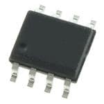
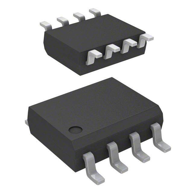
| 描述 | TRANSCEIVER LIN SGL WIRE 8-SOIC |
| 产品分类 | |
| 品牌 | ON Semiconductor |
| 数据手册 | |
| 产品图片 |
|
| 产品型号 | AMIS30600LINI1RG |
| PCN组件/产地 | |
| rohs | 无铅 / 符合限制有害物质指令(RoHS)规范要求 |
| 产品系列 | - |
| 产品目录页面 | |
| 供应商器件封装 | 8-SOIC N |
| 其它名称 | 766-1000-1 |
| 包装 | 剪切带 (CT) |
| 协议 | LIN |
| 双工 | 半 |
| 安装类型 | 表面贴装 |
| 封装/外壳 | 8-SOIC(0.154",3.90mm 宽) |
| 工作温度 | -40°C ~ 125°C |
| 接收器滞后 | 80mV |
| 数据速率 | - |
| 标准包装 | 1 |
| 电压-电源 | 4.75 V ~ 5.25 V |
| 类型 | 收发器 |
| 驱动器/接收器数 | 1/1 |


- 商务部:美国ITC正式对集成电路等产品启动337调查
- 曝三星4nm工艺存在良率问题 高通将骁龙8 Gen1或转产台积电
- 太阳诱电将投资9.5亿元在常州建新厂生产MLCC 预计2023年完工
- 英特尔发布欧洲新工厂建设计划 深化IDM 2.0 战略
- 台积电先进制程称霸业界 有大客户加持明年业绩稳了
- 达到5530亿美元!SIA预计今年全球半导体销售额将创下新高
- 英特尔拟将自动驾驶子公司Mobileye上市 估值或超500亿美元
- 三星加码芯片和SET,合并消费电子和移动部门,撤换高东真等 CEO
- 三星电子宣布重大人事变动 还合并消费电子和移动部门
- 海关总署:前11个月进口集成电路产品价值2.52万亿元 增长14.8%


PDF Datasheet 数据手册内容提取
AMIS-30600 LIN Transceiver General Description The single−wire transceiver AMIS−30600 is a monolithic integrated circuit in a SOIC−8 package. It works as an interface between the protocol controller and the physical bus. The AMIS−30600 is especially suitable to drive the bus line in LIN http://onsemi.com systems in automotive and industrial applications. Further it can be used in standard ISO9141 systems. In order to reduce the current consumption the AMIS−30600 offers PIN ASSIGNMENT a stand−by mode. A wake−up caused by a message on the bus pulls the INH−output high until the device is switched to normal operation mode. The transceiver is implemented in I2T100 technology enabling both RxD 1 8 INH high−voltage analog circuitry and digital functionality to co−exist on the same chip. EN 2 3A 7 VBB 0M auTtohme otAivMe IiSn−−v3e0h6i0c0le pnreotwviodreksi nagn ( IVulNtr)a −resaqfuei resmoleunttiso nb yt op rotovdidaiyn’gs VCC 3 600IS− 6 LIN unlimited short circuit protection in the event of a fault condition. TxD 4 5 GND Features • LIN−Bus Transceiver ♦ LIN compliant to specification rev. 1.3 and rev. 2.0 (Top View) ♦ I2T high−voltage technology ♦ Bus voltage (cid:2) 40 V ♦ Transmission rate up to 20kbaud ORDERING INFORMATION ♦ SOIC−150−8 package See detailed ordering and shipping information in the package • dimensions section on page 9 of this data sheet. Protection ♦ Thermal shutdown ♦ Indefinite short circuit protection to supply and ground • Load dump protection (45 V) • Power Saving ♦ Operating voltage = 4.75 to 5.25 V ♦ Power down supply current < 50 (cid:2)A • EMS Compatibility ♦ Integrated filter and hysteresis for receiver • EMI Compatibility ♦ Integrated slope control for transmitter ♦ Slope control dependant from Vbat to enable maximum capacitive load • These are Pb−Free Devices *For additional information on our Pb−Free strategy and soldering details, please download the ON Semiconductor Soldering and Mounting Techniques Reference Manual, SOLDERRM/D. © Semiconductor Components Industries, LLC, 2014 1 Publication Order Number: December, 2014 − Rev. 9 AMIS−30600/D
AMIS−30600 V V CC BB 3 7 Thermal 8 shutdown State INH & Wake−up 2 Control EN 3 0 10 k k(cid:3) (cid:3) COMP 1 RxD 6 VCC Filter LIN AMIS−30600 4 0 k 4 (cid:3) Slope TxD Control 5 PC20050113.3 GND Figure 1. Block Diagram Master Node Slave Node VBAT IN OUT VBAT IN OUT 5V−reg 5V−reg 10mF 100 nF 10mF 100 nF VBB INH VCC VCC VBBINH VCC VCC 7 8 3 7 8 3 W RxD RxD 1 k 1 1 LIN AMIS− TxD LIN LIN AMIS− TxD LIN 6 4 6 4 30600 controller 30600 controller nF 2 EN 2 EN 1 GND 5 2 GND 5 2 GND GND GND GND KL30 LIN−BUS PC20050113.5 KL31 Figure 2. Application Diagram http://onsemi.com 2
AMIS−30600 Table 1. PIN LIST AND DESCRIPTIONS Pin Name Description 1 RxD Receive data output; low in dominant state 2 EN Enable input; transceiver in normal operation mode when high 3 VCC 5V supply input 4 TxD Transmit data input; low in dominant state; internal 40 k(cid:3) pullup 5 GND Ground 6 LIN LIN bus output/input; low in dominant state; internal 30 k(cid:3) pullup 7 VBB Battery supply input 8 INH Inhibit output; to control a voltage regulator; becomes high when wake−up via LIN bus occurs Table 2. ABSOLUTE MAXIMUM RATINGS Symbol Parameter Conditions Min Max Unit VCC Supply Voltage −0.3 +7 V VBB Battery Supply Voltage −0.3 +40 V VLIN DC Voltage at Pin LIN 0 < VCC < 5.50 V −40 +40 V VINH DC Voltage at Pin INH 0 < VCC < 5.50 V −0.3 VBB + 0.3 V VTxD DC Voltage at Pin TxD 0 < VCC < 5.50 V −0.3 VCC + 0.3 V VRxD DC Voltage at Pin RxD 0 < VCC < 5.50 V −0.3 VCC + 0.3 V VEN DC Voltage at Pin EN 0 < VCC < 5.50 V −0.3 VCC + 0.3 V Vesd(LIN) Electrostatic Discharge Voltage at LIN Pin (Note 1) −4 +4 kV Vesd Electrostatic Discharge Voltage at All Other Pins (Note 1) −4 +4 kV Vtran(LIN) Transient Voltage at Pin LIN (Note 2) −150 +150 V Vtran(VBB) Transient Voltage at Pin VBB (Note 3) −150 +150 V Tamb Ambient Temperature −40 +150 °C Stresses exceeding Maximum Ratings may damage the device. Maximum Ratings are stress ratings only. Functional operation above the Recommended Operating Conditions is not implied. Extended exposure to stresses above the Recommended Operating Conditions may affect device reliability. 1. Standardized Human Body Model system ESD pulses in accordance to IEC 1000.4.2. 2. Applied transient waveforms in accordance with “ISO 7637 parts 1 & 3”, capacitive coupled test pulses 1 (−100 V), 2 (+100 V), 3a (−150 V), and 3b (+150 V). See Figure 8. 3. Applied transient waveforms in accordance with “ISO 7637 parts 1 & 3”, direct coupled test pulses 1 (−100 V), 2 (+75 V), 3a (−150 V), 3b (+150 V), and 5 (+80 V). See Figure 8. Table 3. OPERATING RANGE Symbol Parameter Min Typ Max Unit VCC Supply Voltage 4.75 +5.25 V VBB Battery Supply Voltage 7.3 +18 V TJ Maximum Junction Temperature −40 +150 °C Tjsd Thermal Shutdown Temperature +150 +170 +190 °C Rthj−a Thermal Resistance Junction−to−Ambient 185 °C/W http://onsemi.com 3
AMIS−30600 APPLICATION INFORMATION POWER POWER UP UP VBBa n=d on VBB = on VCC = on INH = H INH = H Rx = LIN data Rx = LIN data EN = H EN = H NORMAL STANDBY EINNH = =L H NORMAL STANDBY EINNH = =L H→ VCC = on MODE MODE Rx = H MODE MODE Rx = H EN = H Wake−up over bus Wake−up over bus t > t wake EN = L t > t wake EN = L SLEEP SLEEP MODE MODE INH = Float INH = Float→ VCC = off Rx = H Rx = Float VCC = on VCC controlled by INH: permanently INH = Float→ VCC = off INH = H→ VCC = on Figure 3. State Diagrams The AMIS−30600 has a slope which depends of the In order to reduce the current consumption, the supply V . This implementation guarantees biggest AMIS−30600 offers a sleep operation mode. This mode is bat slope−time under all load conditions. The rising slope has to selected by switching the enable input EN low (see Figure 4). be slower then the external RC−time−constant, otherwise An external voltage regulator can be controlled via the the slope will be terminated by the RC−time−constant and no INH output in order to minimize the current consumption of longer by the internal slope−control. This would affect the the whole application in sleep mode (see Figure 2). A symmetry of the bus−signal and would limit the maximum wake−up caused by a message on the communication bus allowed bus−speed. automatically enables the voltage regulator by switching the A capacitor of 10 (cid:2)F at the supply voltage input VB INH output high (see Figure 3). In case the voltage regulator buffers the input voltage. In combination with the required control input is not connected to the INH output, or the reverse polarity diode this prevents the device from microcontroller is active respectively, the AMIS−30600 can detecting power down conditions in case of negative be set in normal operation mode by EN = H (see Figure 3). transients on the supply line. http://onsemi.com 4
AMIS−30600 Table 4. DC CHARACTERISTICS VCC = 4.75 V to 5.25 V; VBB = 7.3 V to 18 V,VEN < VENon, TA = −40°C to +125°C; RL = 500 (cid:3) unless specified otherwise. All voltages with respect to ground, positive current flowing into pin, unless otherwise specified. Symbol Parameter Conditions Min Typ Max Unit SUPPLY (Pin VCC and Pin VBB) ICC 5 V Supply Current Dominant; VTxD = 0 V 400 700 μA Recessive; VTxD = VCC 250 500 IBB Battery Supply Current Dominant; VTxD = 0 V 1 1.5 mA Recessive; VTxD = VCC 100 200 μA IBB Battery Supply Current Sleep Mode; VEN = 0 V 35 55 μA ICC 5 V Supply Current Sleep Mode; VEN = 0 V 0.25 1 μA TRANSMITTER DATA INPUT (Pin TxD) VIH High−Level Input Voltage Output Recessive 0.7 x VCC − VCC V VIL Low−Level Input Voltage Output Dominant 0 − 0.3 x VCC V RTxD,pu Pullup Resistor to VCC 24 60 k RECEIVER DATA OUTPUT (Pin RxD) VOH High−Level Output Voltage IRXD = −10 mA 0.8 x VCC VCC V VOL Low−Level Output Voltage IRXD = 5 mA 0 0.2 x VCC V ENABLE INPUT (Pin EN) VEN,on High−Level Input Voltage Normal Mode 0.7 x VCC − VCC V VEN,off Low−Level Input Voltage Low Power Mode 0 − 0.3 x VCC V REN,pd Pulldown Resistor−to−GND 6 10 15 k INHIBIT OUTPUT (Pin INH) VINH,d High−Level Voltage Drop: IINH = − 0.15 mA 0.5 1.0 V VINH,d = VBB − VINH IINH,lk Leakage Current Sleep Mode; VINH = 0 V −5.0 − 5.0 μA BUS LINE (Pin LIN) Vbus,rec Recessive Bus Voltage at Pin VTxD = VCC 0.9 x VBB − VBB V LIN Vbus,dom Dominant Output Voltage at Pin VTxD = 0 V ; VBB = 7.3 V 0 − 1.2 V LIN VTxD = 0 V; VBB = 18 V; 2.0 RL = 500 (cid:3) Ibus,sc Bus Short−Circuit Current Vbus,short = 18 V 40 85 130 mA Ibus,lk Bus Leakage Current VCC = VBB = 0V; Vbus = −8 V −400 −200 μA VCC = VBB = 0V; Vbus = 20 V 5 20 Rbus Bus Pullup Resistance; Note 4 VTxD = 0 V 20 30 47 k(cid:3) Vbus,rd Receiver Threshold: 0.4 x VBB 0.48 x VBB 0.6 x VBB V Recessive−to−Dominant Vbus,dr Receiver Threshold: 0.4 x VBB 0.52 x VBB 0.6 x VBB V Dominant−to−Recessive Vq Receiver Hysteresis Vbus,hys = Vbus,rec − Vbus,dom 0.05 x VBB 0.08 x VBB 0.175 x VBB V VWAKE Wake−up Threshold Voltage 0.4 x VBB 0.6 x VBB V 4. Guaranteed by design. The total resistance of the pullup resistor and the serial diode is measured on ATE. http://onsemi.com 5
AMIS−30600 Table 5. AC ELECTRICAL CHARACTERISTICS ACCORDING TO LIN V13 VCC = 4.75 V to 5.25 V; VBB = 7.3 V to 18 V,VEN < VENon, TA = −40°C to +125°C; RL = 500 (cid:3) unless otherwise specified. Load for slope definitions (typical loads) = [L1] 1 nF 1 k(cid:3) / [L2] 6.8 nF 600 (cid:3) / [L3] 10 nF 500 (cid:3). Symbol Parameter Conditions Min Typ Max Unit t_slope_F Slope Time Falling Edge; (Note 5) See Figure 5 4 − 24 (cid:2)s t_slope_R Slope Time Rising Edge; (Note 5) See Figure 5 4 − 24 (cid:2)s t_slope_Sym Slope Time Symmetry; (Note 5) t_slope_F − t_slope_R −8 − +8 (cid:2)s T_rec_F Propagation Delay Bus Dominant to See Figures 4 and 5 2 6 (cid:2)s RxD = Low; (Note 6) T_rec_R Propagation Delay Bus Recessive to See Figures 4 and 5 6 6 (cid:2)s RxD = High; (Note 6) tWAKE Wake−up Delay Time 30 100 200 (cid:2)s 5. Guaranteed by design; not measured for all supply/load combinations on ATE. 6. Not measured on ATE. Table 6. AC ELECTRICAL CHARACTERISTICS ACCORDING TO LIN v2.0 VCC = 4.75 V to 5.25 V; VBB = 7.3 V to 18 V,VEN < VENon, TA = −40°C to +125°C; RL = 500 (cid:3) unless otherwise specified. Load for slope definitions (typical loads) = [L1] 1 nF 1 k(cid:3) / [L2] 6.8 nF 600 (cid:3) / [L3] 10 nF 500 (cid:3). Symbol Parameter Conditions Min Typ Max Unit DYNAMIC RECEIVER CHARACTERISTICS ACCORDING TO LIN v2.0 trx_pdr Propagation Delay Bus Dominant to See Figure 6 6 (cid:2)s RxD = Low; (Note 7) trx_pdf Propagation Delay Bus Recessive to See Figure 6 6 (cid:2)s RxD = High; (Note 7) trx_sym Symmetry of Receiver Propagation Delay trx_pdr − trx_pdf −2 − +2 (cid:2)s DYNAMIC TRANSMITTER CHARACTERISTICS ACCORDING TO LIN v2.0 D1 Duty Cycle 1 = tBus_rec(min)/(2 x tBit); 0.396 0.5 See Figure D1 Duty Cycle 1 = tBus_rec(min)/(2 x tBit); THRec(max) = 0.744 x Vbat; 0.366 0.5 See Figure 6 THDom(max) = 0.581 x Vbat;Vbat = 7.0 V to 18 V; tBit = 50 (cid:2)s THRec(max) = 0.744 x Vbat; THDom(max) = 0.581 x Vbat;Vbat = 7.0V; tBit = 50 (cid:2)s; tamb = −40°C D2 Duty Cycle 2 = tBus_rec(max)/(2 x tBit); THRec(min) = 0.284 x Vbat; 0.5 0.581 See Figure 6 THDom(min) = 0.422 x Vbat;Vbat = 7.6 V to 18 V; tBit = 50 (cid:2)s; 7. Not measured on ATE. http://onsemi.com 6
AMIS−30600 Vbat VBB 100 nF 7 +5V 3 RL 100 nF 2 AMIS− 6 LIN EN 30600 Load RL CL CL L1 1k(cid:3) 1nF INH 3 4 L2 600 (cid:3) 6.8nF TxD 1 5 L3 500 (cid:3) 10 nF RxD GND 20 pF PD200801.213 Figure 4. Test Circuit for Timing Characteristics LIN 50% t RxD T_rec_F T_rec_R 50% 50% t LIN PC2004120.61 60% 60% 40% 40% t T_slope_F T_slope_R PC20041206.2 Figure 5. Timing Diagram for AC Characteristics According to LIN 1.3 http://onsemi.com 7
AMIS−30600 TxD tBIT tBIT 50% t LIN tBUS_DOM(max) tBUS_REC(min) THREC(max) Thresholds THDOM(max) receiver1 THREC(max) Thresholds THDOM(max) receiver2 t tBUS_DOM(min) tBUS_REC(max) RxD (receiver2) 50% trx_pdf trx_pdr t PD20080319.1 Figure 6. Timing Diagram for AC Characteristics According to LIN 2.0 +13.5 V 100 nF VBB 7 V CC +5.25 V 3 Transient 1 k(cid:3) 100 nF Generator AMIS− LIN TxD 6 4 30600 1 nF 1 nF EN 2 3 INH 1 5 RxD GND 20 pF PC20050113.2 Figure 7. Test Circuit for Transient Measurements http://onsemi.com 8
AMIS−30600 DEVICE ORDERING INFORMATION Part Number Temperature Range Package Type Shipping† AMIS30600LINI1G −40°C − 125°C SOIC−8 96 Tube / Tray (Pb−Free) AMIS30600LINI1RG −40°C − 125°C SOIC−8 3000 / Tape & Reel (Pb−Free) †For information on tape and reel specifications, including part orientation and tape sizes, please refer to our Tape and Reel Packaging Specifications Brochure, BRD8011/D. http://onsemi.com 9
AMIS−30600 PACKAGE DIMENSIONS SOIC 8 CASE 751AZ ISSUE A http://onsemi.com 10
AMIS−30600 ON Semiconductor and are registered trademarks of Semiconductor Components Industries, LLC (SCILLC). SCILLC owns the rights to a number of patents, trademarks, copyrights, trade secrets, and other intellectual property. A listing of SCILLC’s product/patent coverage may be accessed at www.onsemi.com/site/pdf/Patent−Marking.pdf. SCILLC reserves the right to make changes without further notice to any products herein. SCILLC makes no warranty, representation or guarantee regarding the suitability of its products for any particular purpose, nor does SCILLC assume any liability arising out of the application or use of any product or circuit, and specifically disclaims any and all liability, including without limitation special, consequential or incidental damages. “Typical” parameters which may be provided in SCILLC data sheets and/or specifications can and do vary in different applications and actual performance may vary over time. All operating parameters, including “Typicals” must be validated for each customer application by customer’s technical experts. SCILLC does not convey any license under its patent rights nor the rights of others. SCILLC products are not designed, intended, or authorized for use as components in systems intended for surgical implant into the body, or other applications intended to support or sustain life, or for any other application in which the failure of the SCILLC product could create a situation where personal injury or death may occur. Should Buyer purchase or use SCILLC products for any such unintended or unauthorized application, Buyer shall indemnify and hold SCILLC and its officers, employees, subsidiaries, affiliates, and distributors harmless against all claims, costs, damages, and expenses, and reasonable attorney fees arising out of, directly or indirectly, any claim of personal injury or death associated with such unintended or unauthorized use, even if such claim alleges that SCILLC was negligent regarding the design or manufacture of the part. SCILLC is an Equal Opportunity/Affirmative Action Employer. This literature is subject to all applicable copyright laws and is not for resale in any manner. PUBLICATION ORDERING INFORMATION LITERATURE FULFILLMENT: N. American Technical Support: 800−282−9855 Toll Free ON Semiconductor Website: www.onsemi.com Literature Distribution Center for ON Semiconductor USA/Canada P.O. Box 5163, Denver, Colorado 80217 USA Europe, Middle East and Africa Technical Support: Order Literature: http://www.onsemi.com/orderlit Phone: 303−675−2175 or 800−344−3860 Toll Free USA/Canada Phone: 421 33 790 2910 Fax: 303−675−2176 or 800−344−3867 Toll Free USA/Canada Japan Customer Focus Center For additional information, please contact your local Email: orderlit@onsemi.com Phone: 81−3−5817−1050 Sales Representative http://onsemi.com AMIS−30600/D 11
Mouser Electronics Authorized Distributor Click to View Pricing, Inventory, Delivery & Lifecycle Information: O N Semiconductor: AMIS30600LINI1G AMIS30600LINI1RG